

Page 1
General Description
The MAX15022 is a dual-output, pulse-width-modulated
(PWM), step-down DC-DC regulator with dual LDO controllers. The device operates from 2.5V to 5.5V and
each output can be adjusted from 0.6V to the input
supply (V
AVIN
). The MAX15022 delivers up to 4A (regulator 1) and 2A (regulator 2) of output current with two
LDO controllers that can be used to drive two external
PNP transistors to provide two additional outputs. This
device offers the ability to adjust the switching frequency from 500kHz to 4MHz and provides the capability of
optimizing the design in terms of size and performance.
The MAX15022 utilizes a voltage-mode control scheme
with external compensation to provide good noise
immunity and maximum flexibility in selecting inductor
values and capacitor types. The dual switching regulators operate 180° out-of-phase, thereby reducing the
RMS input ripple current and thus the size of the input
bypass capacitor significantly.
The MAX15022 offers the ability to track (coincident or
ratiometric) or sequence during power-up and powerdown operation. When sequencing, it powers up glitchfree into a prebiased output.
Additional features include an internal undervoltage
lockout with hysteresis and a digital soft-start/soft-stop
for glitch-free power-up and power-down. Protection
features include lossless cycle-by-cycle current limit,
hiccup-mode output short-circuit protection, and thermal shutdown.
The MAX15022 is available in a space-saving, 5mm x
5mm, 28-pin TQFN-EP package and is specified for
operation from -40°C to +125°C temperature range.
Applications
RFID Reader Cards
Power-over-Ethernet (PoE) IP Phones
Automotive Multimedia
Multivoltage Supplies
Networking/Telecom
Features
o 2.5V to 5.5V Input-Voltage Range
o Dual-Output Synchronous Buck Regulators
o Integrated Switches for 4A and 2A Output
Currents
o 180° Out-Of-Phase Operation
o Output Voltage Adjustable from 0.6V to V
AVIN
o Two LDO Controllers
o Lossless, Cycle-by-Cycle Current Sensing
o External Compensation for Maximum Flexibility
o Digital Soft-Start and Soft-Stop for Tracking
Applications
o Digital Soft-Start into a Prebiased Load for
Sequencing Applications
o Sequencing or Coincident/Ratiometric Tracking
o Programmable Switching Frequency from 500kHz
to 4MHz
o Thermal Shutdown and Hiccup-Mode Short-
Circuit Protection
o 30µA Shutdown Current
o 100% Maximum Duty Cycle
o Space-Saving (5mm x 5mm) 28-Pin TQFN
Package
MAX15022
Dual, 4A/2A, 4MHz, Step-Down DC-DC
Regulator with Dual LDO Controllers
________________________________________________________________
Maxim Integrated Products
1
Pin Configuration
Ordering Information
19-4107; Rev 0; 5/08
For pricing, delivery, and ordering information, please contact Maxim Direct at 1-888-629-4642,
or visit Maxim’s website at www.maxim-ic.com.
EVALUATION KIT
AVAILABLE
PART TEMP RANGE PIN-PACKAGE
MAX15022ATI+
-40°C to +125°C 28 TQFN-EP*
+
Denotes a lead-free package.
*
EP = Exposed pad.
TOP VIEW
EN4
LX2
PVIN2
18
4
PGND2
DVDD2
EN3
*EP
567
14
FB3
B3
13
12
COMP1
FB1
11
10
EN1
DVDD1
9
8
PGND1
COMP2
FB2
EN2
SGND
AVIN
FB4
2021 19 17 16 15
B4
22
23
24
25
26
27
28
RT
1+2
MAX15022
3
*EP = EXPOSED PAD.
SEL
LX1
PGND1
THIN QFN
(5mm x 5mm)
PVIN1
PVIN1
LX1
PGND1
Page 2
MAX15022
Dual, 4A/2A, 4MHz, Step-Down DC-DC
Regulator with Dual LDO Controllers
2 _______________________________________________________________________________________
ABSOLUTE MAXIMUM RATINGS
ELECTRICAL CHARACTERISTICS
(V
AVIN
= V
PVIN_
= V
DVDD_
= 3.3V, V
PGND_
= V
SGND
= 0V, RT= 25kΩ, and TA= TJ= -40°C to +125°C, unless otherwise noted.
Typical values are at T
A
= +25°C.) (Note 3)
Stresses beyond those listed under “Absolute Maximum Ratings” may cause permanent damage to the device. These are stress ratings only, and functional
operation of the device at these or any other conditions beyond those indicated in the operational sections of the specifications is not implied. Exposure to
absolute maximum rating conditions for extended periods may affect device reliability.
Note 1: LX has internal diodes to PGND_ and PVIN_. Applications that forward bias these diodes should take care not to exceed
the IC’s package power dissipation limits.
Note 2: Package thermal resistances were obtained using the method described in JEDEC specification JESD51-7, using a four-
layer board. For detailed information on package thermal considerations see www.maxim-ic.com/thermal-tutorial
.
AVIN, PVIN_, B_, DVDD_, EN_, FB_, RT,
SEL to SGND .........................................................-0.3V to +6V
COMP_ to SGND .....................................-0.3V to (V
AVIN
+ 0.3V)
PGND_ to SGND ...................................................-0.3V to +0.3V
LX Current (Note 1)
Regulator 1...............................................................................6A
Regulator 2...............................................................................3A
Current into Any Pin Other than PVIN_,
LX_ and PGND_.............................................................±50mA
Continuous Power Dissipation (T
A
= +70°C)
28-Pin TQFN (derate 34.5mW/°C above +70°C) .....2758.6mW
Junction-to-Case Thermal Resistance (θ
JC
)(Note 2) .........2°C/W
Junction-to-Ambient Thermal Resistance (θ
JA
)(Note 2) ..29°C/W
Operating Temperature Range .........................-40°C to +125°C
Junction Temperature......................................................+150°C
Storage Temperature Range .............................-60°C to +150°C
Lead Temperature (soldering, 10s) .................................+300°C
SYSTEM SPECIFICATIONS
Input-Voltage Range
Undervoltage Lockout Threshold AVIN rising 2.1 2.2 2.3 V
Undervoltage Lockout Hysteresis 0.12 V
Operating Supply Current V
Shutdown Supply Current V
PWM DIGITAL SOFT-START/SOFT-STOP
Soft-Start/Soft-Stop Duration 4096
Reference Voltage Steps 64 Steps
PWM ERROR AMPLIFIERS
FB1, FB2 Input Bias Current -1 +1 μA
FB1, FB2 Voltage Set-Point 0.593 0.599 0.605 V
COMP1, COMP2 Voltage Range I
Error-Amplifier Open-Loop Gain 80 dB
Error-Amplifier Unity-Gain
Bandwidth
PARAMETER SYMBOL CONDITIONS MIN TYP MAX UNITS
V
= V
AVIN
V
DVDD2
= 1.3V, V
EN_
= 0V 30 65 μA
EN_
_ = -250μA to +250μA 0.3 V
COMP
PVIN1
= V
FB_
= V
PVIN2
= 0.8V 3.5 6 mA
DVDD1
=
2.5 5.5 V
AVIN
12 MHz
- 0.5 V
Clock
Cycles
Page 3
MAX15022
Dual, 4A/2A, 4MHz, Step-Down DC-DC
Regulator with Dual LDO Controllers
_______________________________________________________________________________________ 3
ELECTRICAL CHARACTERISTICS (continued)
(V
AVIN
= V
PVIN_
= V
DVDD_
= 3.3V, V
PGND_
= V
SGND
= 0V, RT= 25kΩ, and TA= TJ= -40°C to +125°C, unless otherwise noted.
Typical values are at T
A
= +25°C.) (Note 3)
LDO CONTROLLERS
FB3, FB4 Input Bias Current -250 +250 nA
FB3, FB4 Voltage Set-point 5mA sink current, VB_ = 0.5V to 5.5V 0.585 0.600 0.615 V
FB3, FB4 to B3, B4
Transconductance
B3, B4 Driver Sink Current V
LDO Soft-Start Duration
LDO Reference Voltage Steps 64 Steps
POWER MOSFETS
Regulator 1 p-Channel MOSFET
R
DSON
Regulator 1 n-Channel MOSFET
R
DSON
Regulator 1 Gate Charge V
Maximum LX1 RMS Current 4A
Regulator 2 p-Channel MOSFET
R
DSON
Regulator 2 n-Channel MOSFET
R
DSON
Regulator 2 Gate Charge V
Maximum LX2 RMS Current 2A
PWM CURRENT LIMIT AND HICCUP MODE
Regulator 1 Peak Current Limit
Regulator 1 Valley Current Limit
Regulator 2 Peak Current Limit
Regulator 2 Valley Current Limit
Number of Cumulative CurrentLimit Events to Hiccup
Number of Consecutive Noncurrent
Limit Cycles to Clear N
Hiccup Timeout N
PARAMETER SYMBOL CONDITIONS MIN TYP MAX UNITS
CL
2.5mA to 10mA sink current,
V
= 0.5V to 5.5V
B_
FB3, VFB4
V
DVDD1
V
DVDD1
DVDD1
V
DVDD2
V
DVDD2
DVDD2
V
PVIN
V
PVIN
V
PVIN
V
PVIN
V
PVIN
V
PVIN
V
PVIN
V
PVIN
N
CL
N
CLR
HT
= 0V, VB_ = 0.5V to 5.5V 20 mA
= 5V 50 90 mΩ
= 5V 30 50 mΩ
= 5V 8 nC
= 5V 100 180 mΩ
= 5V 60 100 mΩ
= 5V 4 nC
= V
= V
= V
= V
= V
= V
= V
= V
= 3.3V 4.5 4.9 5.3
AVIN
= 2.5V 3.40 3.65 3.95
AVIN
= 3.3V 4.0 5.0 5.65
AVIN
= 2.5V 3.0 3.7 4.25
AVIN
= 3.3V 2.25 2.45 2.65
AVIN
= 2.5V 1.70 1.85 1.98
AVIN
= 3.3V 2.0 2.5 2.83
AVIN
= 2.5V 1.5 1.85 2.13
AVIN
0.56 1.20 2.30 S
512
4
3
8192
Clock
Cycles
Clock
Cycles
Clock
Cycles
Clock
Cycles
A
A
A
A
Page 4
MAX15022
Dual, 4A/2A, 4MHz, Step-Down DC-DC
Regulator with Dual LDO Controllers
4 _______________________________________________________________________________________
ELECTRICAL CHARACTERISTICS (continued)
(V
AVIN
= V
PVIN_
= V
DVDD_
= 3.3V, V
PGND_
= V
SGND
= 0V, RT= 25kΩ, and TA= TJ= -40°C to +125°C, unless otherwise noted.
Typical values are at T
A
= +25°C.) (Note 3)
Note 3: Specifications are 100% production tested at TA= +25°C and TA= +125°C. Maximum and minimum specifications over
temperature are guaranteed by design.
Note 4: When operating with V
AVIN
= 2.5V, the maximum operating frequency should be derated to 3MHz.
ENABLE/SEL
EN_ Threshold V
EN_ Hysteresis 0.12 V
EN_ Input Current -2.5 +2.5 μA
SEL High Threshold 0.85 x V
SEL Low Threshold 0.2 x V
SEL Input Bias Current Present only during startup -100 +100 μA
OSCILLATOR
Switching Frequency Range f
Oscillator Accuracy
Phase Shift Between Regulators 180 Degrees
RT Current 0 < VRT < 1.067V 31.30 32.00 32.58 μA
RT Voltage Range V
Minimum Controllable On-Time 60 ns
Minimum Controllable Off-Time 60 ns
PWM Ramp Amplitude V
PWM Ramp Valley 0.3 V
THERMAL SHUTDOWN
Thermal Shutdown Temperature Temperature rising +160 °C
Thermal Shutdown Hysteresis 15 °C
PARAMETER SYMBOL CONDITIONS MIN TYP MAX UNITS
SW
RT
rising 1.207 1.225 1.243 V
EN_
f
= 4MHz x [VRT(V)/1.067(V)] (Note 4) 4000 kHz
SW
fSW ≤ 1500kHz -6 +6
f
> 1500kHz -10 +10
SW
0.130 1.067 V
AVIN
/4 V
AVIN
AVIN
V
V
%
Page 5
MAX15022
Dual, 4A/2A, 4MHz, Step-Down DC-DC
Regulator with Dual LDO Controllers
_______________________________________________________________________________________
5
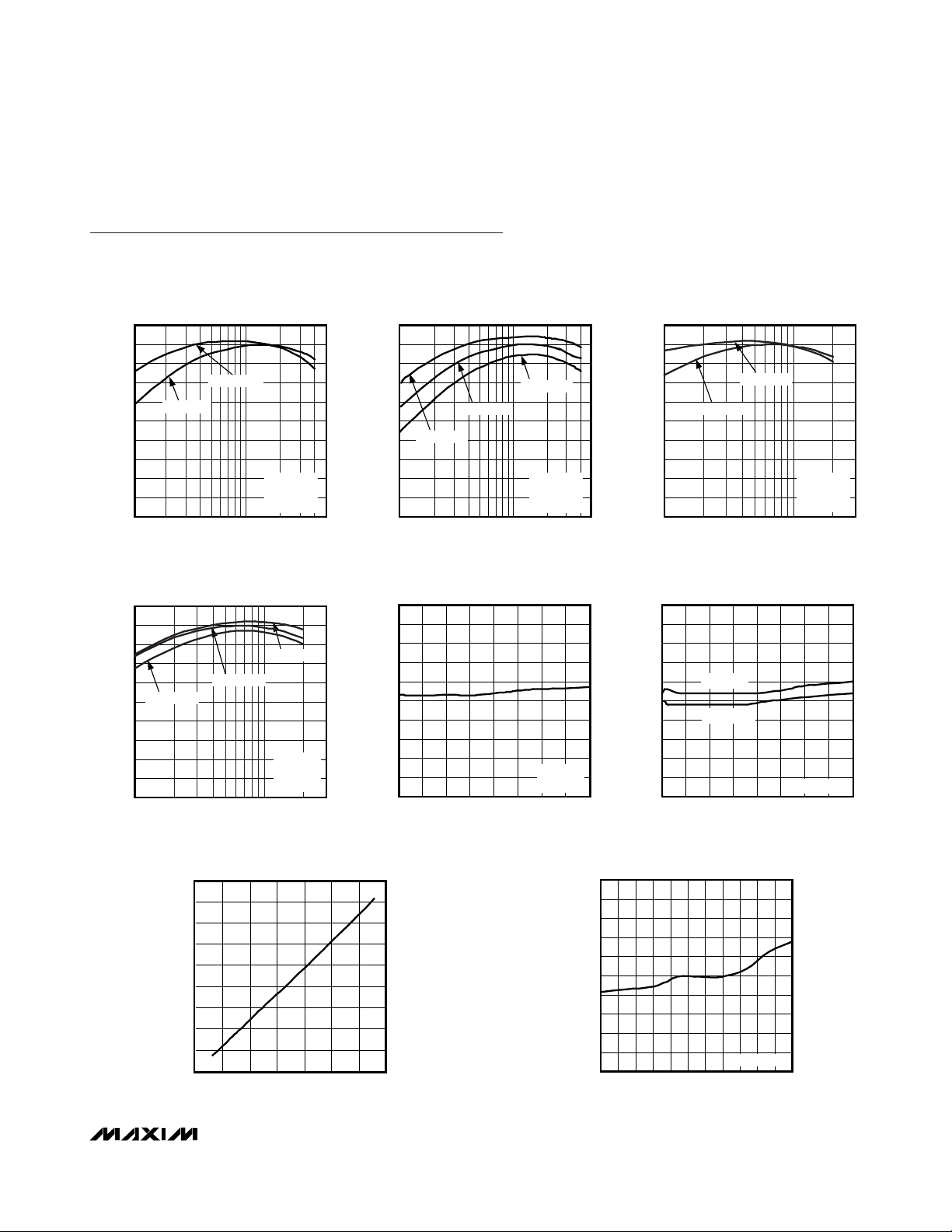
Typical Operating Characteristics
(V
AVIN
= V
DVDD1
= V
DVDD2
= V
PVIN1
= V
PVIN2
= 5V, V
OUT1
= 3.3V, V
OUT2
= 1.5V, V
PGND_
= 0V, RT= 16.5kΩ. TA= +25°C, unless
otherwise noted.)
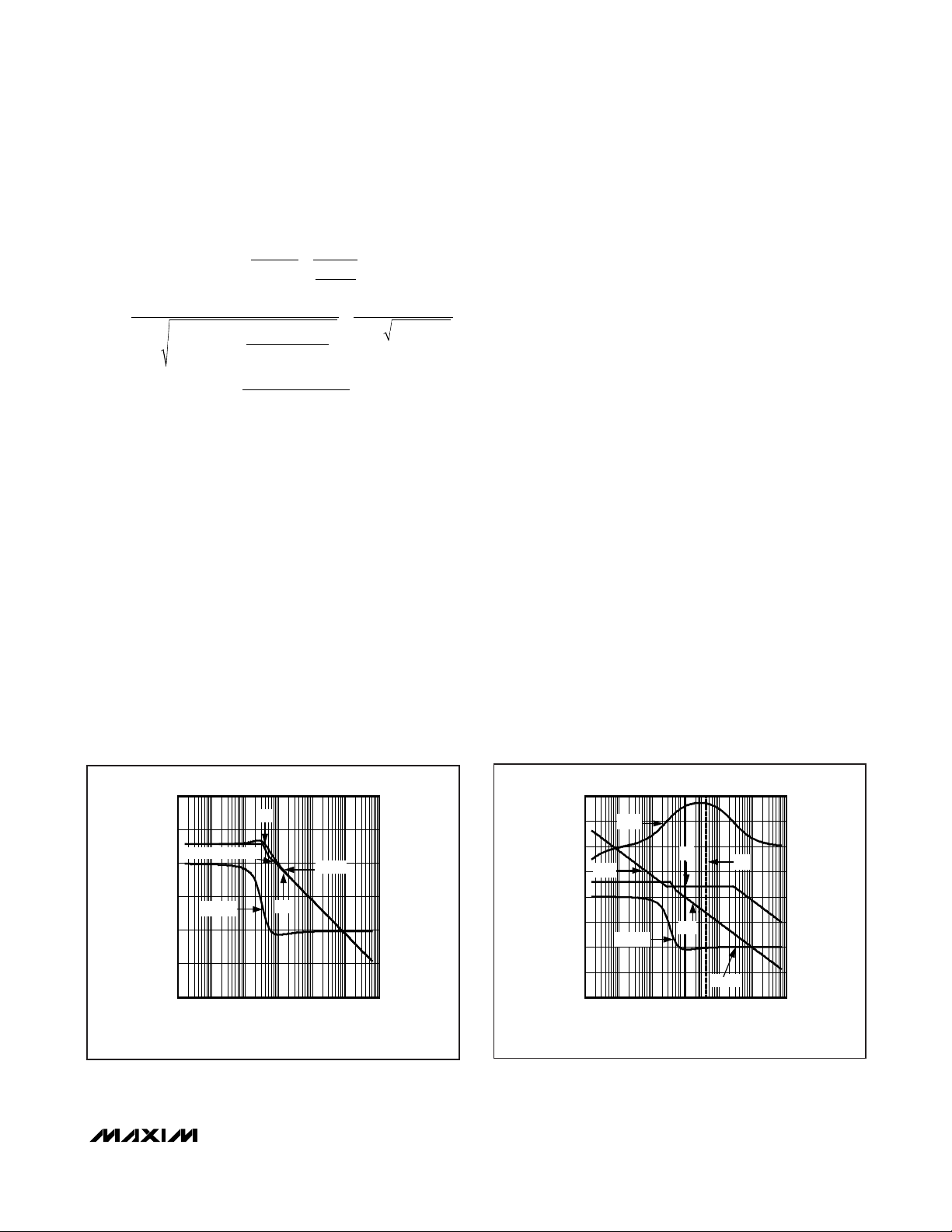
CHANNEL 1 EFFICIENCY
vs. LOAD CURRENT
MAX15022 toc01
LOAD CURRENT (mA)
EFFICIENCY (%)
1000
10
20
30
40
50
60
70
80
90
100
0
100 5000
V
PVIN1
= 3.3V
V
PVIN1
= 5V
V
OUT1
= 1.8V
f
SW
= 2MHz
EN2 = 0V
CHANNEL 1 EFFICIENCY
vs. LOAD CURRENT
MAX15022 toc02
LOAD CURRENT (mA)
EFFICIENCY (%)
1000
10
20
30
40
50
60
70
80
90
100
0
100 5000
V
PVIN1
= 5V
f
SW
= 2MHz
EN2 = 0V
V
OUT1
= 3.3V
V
OUT1
= 1.8V
V
OUT1
= 1.0V
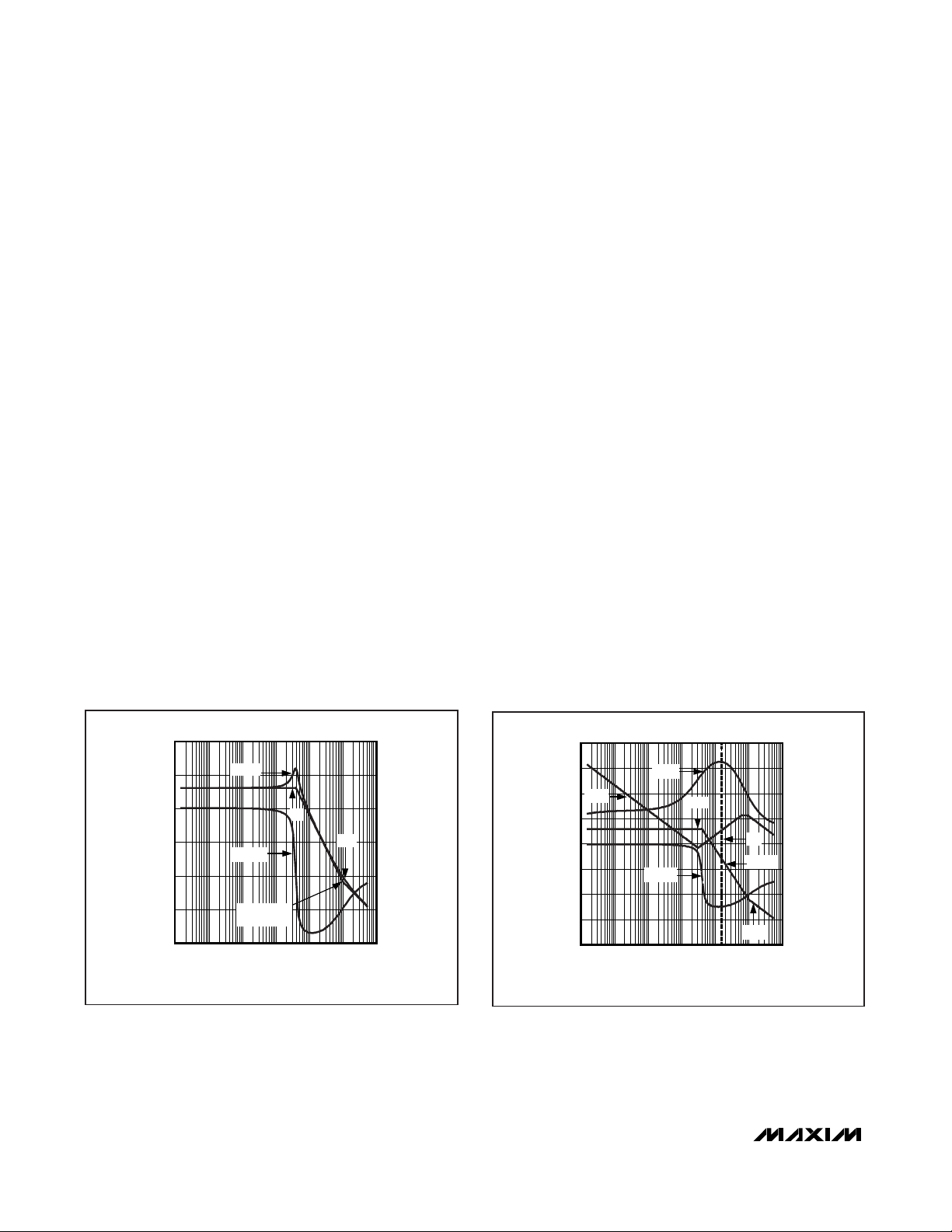
CHANNEL 2 EFFICIENCY
vs. LOAD CURRENT
MAX15022 toc03
LOAD CURRENT (mA)
EFFICIENCY (%)
1000
10
20
30
40
50
60
70
80
90
100
0
100 3000
P
VIN2
= 5V
P
VIN2
= 3.3V
V
OUT2
= 1.5V
f
SW
= 2MHz
EN1 = 0V
CHANNEL 2 EFFICIENCY
vs. LOAD CURRENT
MAX15022 toc04
LOAD CURRENT (mA)
EFFICIENCY (%)
1000
10
20
30
40
50
60
70
80
90
100
0
100 3000
V
OUT2
= 1.0V
V
OUT2
= 1.5V
V
OUT2
= 2.5V
V
PVIN2
= 5V
f
SW
= 2MHz
EN1 = 0V
CHANNEL 1
LOAD REGULATION
MAX15022 toc05
LOAD CURRENT (A)
V
OUT1
(V)
3.302
3.304
3.306
3.308
3.310
3.312
3.314
3.316
3.318
3.320
3.300
3.53.02.52.01.51.00.50 4.0
V
PVIN1
= 5V
f
SW
= 2MHz
CHANNEL 2
LOAD REGULATION
MAX15022 toc06
LOAD CURRENT (A)
V
OUT2
(V)
1.251.00
0.75
0.50
0.25
1.5025
1.5030
1.5035
1.5040
1.5045
1.5050
1.5055
1.5060
1.5065
1.5070
1.5020
0
1.50 1.75 2.00
fSW = 2MHz
V
PVIN2
= 5V
V
PVIN2
= 3.3V
SWITCHING FREQUENCY
vs. RT RESISTANCE
MAX15022 toc07
RT RESISTANCE (kΩ)
SWITCHING FREQUENCY (MHz)
35
30
20 2510
15
5
0.5
1.0
1.5
2.0
2.5
3.0
3.5
4.0
4.5
0
0
SWITCHING FREQUENCY
vs. TEMPERATURE
MAX15022 toc08
TEMPERATURE (°C)
CHANGE IN SWITCHING FREQUENCY (%)
1109565 80-10 5 20 35 50-25
-0.4
-0.3
-0.2
-0.1
0
0.1
0.2
0.3
0.4
0.5
-0.5
-40 125
fSW = 2MHz
Page 6
MAX15022
Dual, 4A/2A, 4MHz, Step-Down DC-DC
Regulator with Dual LDO Controllers
6 _______________________________________________________________________________________
Typical Operating Characteristics (continued)
(V
AVIN
= V
DVDD1
= V
DVDD2
= V
PVIN1
= V
PVIN2
= 5V, V
OUT1
= 3.3V, V
OUT2
= 1.5V, V
PGND_
= 0V, RT= 16.5kΩ. TA= +25°C, unless
otherwise noted.)
EN_ THRESHOLD
vs. TEMPERATURE
MAX15022 toc12
TEMPERATURE (°C)
EN_ THRESHOLD (V)
11095-25 -10 5 35 50 6520 80-40 125
1.215
1.220
1.225
1.230
1.235
1.240
1.245
1.250
1.255
1.260
1.210
5.00
4.75
4.50
4.25
4.00
3.75
3.50
3.25
QUIESCENT CURRENT (mA)
3.00
2.75
2.50
1.030
1.025
1.020
1.015
1.010
1.005
1.000
0.995
0.990
0.985
NORMALIZED UVLO THRESHOLD
0.980
0.975
0.970
QUIESCENT CURRENT
vs. TEMPERATURE
NO SWITCHING
-40 125
TEMPERATURE (°C)
1109565 80-10 5 20 35 50-25
NORMALIZED UNDERVOLTAGE LOCKOUT
THRESHOLD vs. TEMPERATURE
V
(NOM) = 2.2V
UVLO
-40 125
TEMPERATURE (°C)
1109565 80-10 5 20 35 50-25
MAX15022 toc09
MAX15022 toc11
27
26
25
24
23
22
21
20
19
18
17
16
SWITCHING CURRENT (mA)
15
14
13
12
-40 125
SWITCHING CURRENT
vs. TEMPERATURE
REGULATOR 1 ENABLED
V
REGULATOR 2 ENABLED
V
OUT2
TEMPERATURE (°C)
OUT1
= 3.3V
= 1.5V
MAX15022 toc10
1109565 80-10 5 20 35 50-25
COINCIDENT TRACKING SOFT-START
1ms/div
MAX15022 toc13
V
AVIN
5V/div
0V
V
OUT1
1V/div
V
OUT2
1V/div
0V
COINCIDENT TRACKING SOFT-STOP
V
OUT1
EN1
V
OUT2
400μs/div
MAX15022 toc14
V
AVIN
5V/div
0V
1V/div
0V
Page 7
MAX15022
Dual, 4A/2A, 4MHz, Step-Down DC-DC
Regulator with Dual LDO Controllers
_______________________________________________________________________________________
7
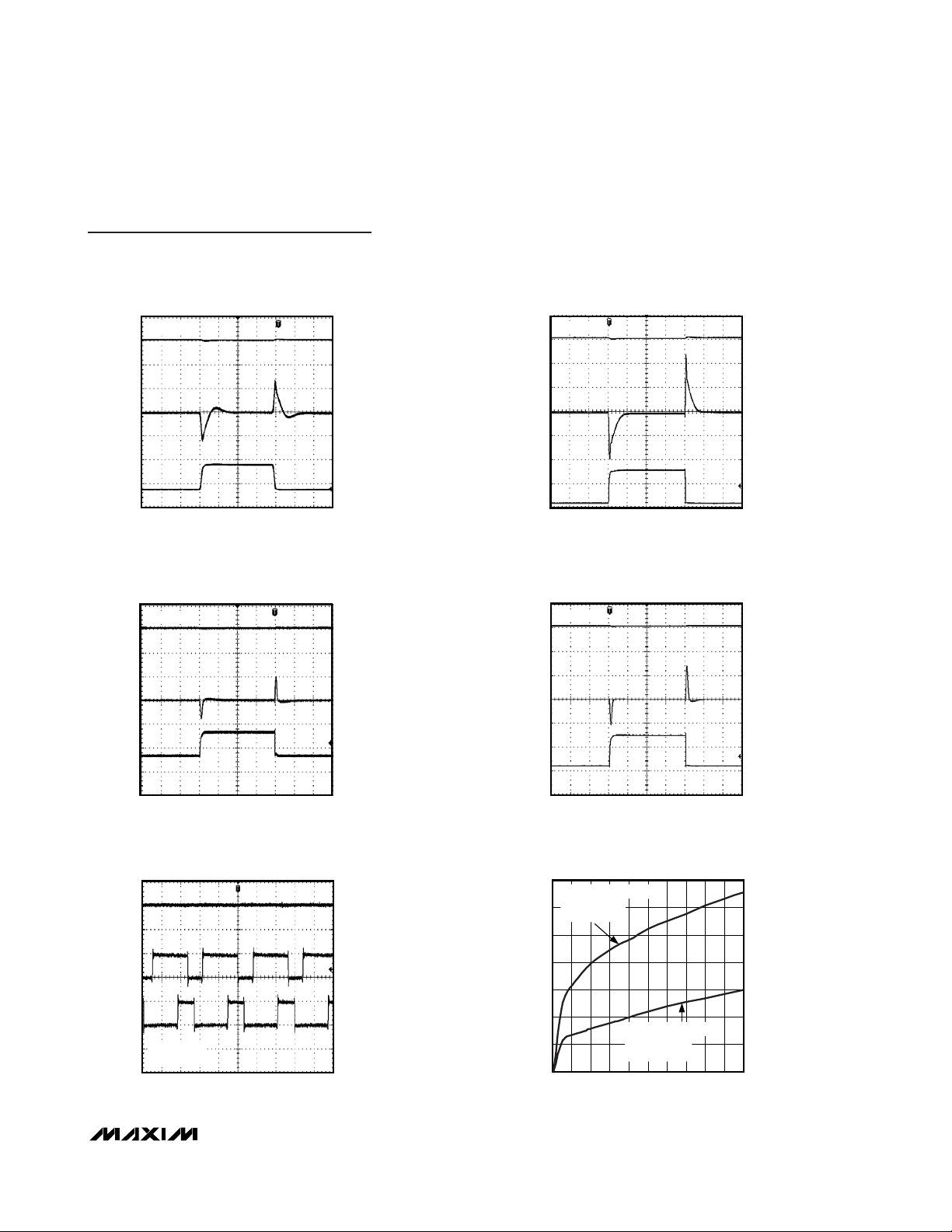
Typical Operating Characteristics (continued)
(V
AVIN
= V
DVDD1
= V
DVDD2
= V
PVIN1
= V
PVIN2
= 5V, V
OUT1
= 3.3V, V
OUT2
= 1.5V, V
PGND_
= 0V, RT= 16.5kΩ. TA= +25°C, unless
otherwise noted.)
CHANNEL 1 LOAD STEP RESPONSE
MAX15022 toc15
V
PVIN1
5V/div
V
OUT1
3.3V, AC-COUPLED
100mV/div
I
OUT1
2A/div
0V
0A
20μs/div
EN2 = 0V
CHANNEL 1 LOAD STEP RESPONSE
MAX15022 toc16
V
PVIN1
5V/div
V
OUT1
3.3V, AC-COUPLED
100mV/div
I
OUT1
2A/div
0V
0A
20μs/div
EN2 = 0V
CHANNEL 2 LOAD STEP RESPONSE
EN1 = 0V
180° OUT-OF-PHASE OPERATION
IOUT1 = 3A
IOUT2 = 1.5A
20μs/div
200ns/div
MAX15022 toc17
MAX15022 toc19
V
PVIN2
5V/div
0V
V
OUT2
1.5V, AC-COUPLED
100mV/div
I
OUT2
1A/div
0A
PVIN1 = PVIN2
5V/div
0V
V
LX1
5V/div
0V
V
LX2
5V/div
0V
CHANNEL 2 LOAD STEP RESPONSE
EN1 = 0V
20μs/div
CHANNEL 3 AND CHANNEL 4 OUTPUT-
VOLTAGE DEVIATION vs. LOAD CURRENT
14
CHANNEL 3, VIN = 3.3V,
= 2.5V
V
OUT3
12
NJT403OP PNP
10
8
6
4
OUTPUT-VOLTAGE DEVIATION (mV)
2
0
0 500
CHANNEL 4, VIN = 2.5V,
= 1.5V
V
OUT4
NJT403OP PNP
LOAD CURRENT (mA)
MAX15022 toc18
450 40035030025020015010050
V
PVIN2
5V/div
0V
V
OUT2
1.5V, AC-COUPLED
100mV/div
I
OUT2
1A/div
0A
MAX15022 toc20
Page 8
MAX15022
Dual, 4A/2A, 4MHz, Step-Down DC-DC
Regulator with Dual LDO Controllers
8 _______________________________________________________________________________________
Pin Description
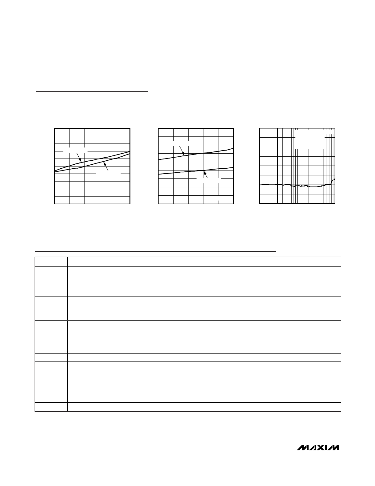
Typical Operating Characteristics (continued)
(V
AVIN
= V
DVDD1
= V
DVDD2
= V
PVIN1
= V
PVIN2
= 5V, V
OUT1
= 3.3V, V
OUT2
= 1.5V, V
PGND_
= 0V, RT= 16.5kΩ. TA= +25°C, unless
otherwise noted.)
2.500
2.495
2.490
2.485
2.480
2.475
2.470
OUTPUT VOLTAGE (V)
2.465
2.460
2.455
2.450
2.90 5.50
CHANNEL 3 OUTPUT VOLTAGE
vs. INPUT VOLTAGE
I
= 10mA
OUT3
I
OUT3
SUPPLY VOLTAGE (V)
= 500mA
V
OUT3
4.984.463.943.42
= 2.5V
MAX15022 toc21
CHANNEL 4 OUTPUT VOLTAGE
vs. INPUT VOLTAGE
1.215
1.210
I
= 500mA
1.205
1.200
1.195
1.190
1.185
OUTPUT VOLTAGE (V)
1.180
1.175
1.170
OUT4
I
OUT4
2.90 5.50
SUPPLY VOLTAGE (V)
= 10mA
V
= 1.5V
OUT4
4.984.463.943.42
-10
MAX15022 toc22
-20
-30
-40
PSRR (dB)
-50
-60
-70
-80
LDO POWER-SUPPLY REJECTION RATIO
0
10 1000
V
= 3.3V, V
IN
= 10mA,
I
OUT3
100mV
APPLIED TO V
100
FREQUENCY (Hz)
P-P
OUT3
SIGNAL
IN
= 2.5V,
MAX15022 toc23
PIN NAME FUNCTION
Track/Sequence Select Input. Connect SEL to SGND to configure the device as a sequencer. Connect
1 SEL
2, 7, 8 PGND1
3, 6 LX1
4, 5 PVIN1
9 DVDD1 Switch Driver Supply for Regulator 1. Connect externally to PVIN1.
10 EN1
11 FB1
12 COMP1 Error-Amplifier Output for Regulator 1. Connect COMP1 to the compensation feedback network.
SEL to AVIN for tracking with output 1 as the master. Leave SEL unconnected for tracking with output 2
as the master. Use the output with the higher voltage as the master and the output with the lower voltage
as the slave.
Power Ground Connection for Regulator 1. Connect the negative terminals of the input and output filter
capacitors to PGND1. Connect PGND1 externally to SGND at a single point, typically at the negative
terminal of the input bypass capacitor.
Inductor Connection for Regulator 1. LX1 is the drain connection of the internal high-side p-channel
MOSFET and the drain connection of the internal synchronous n-channel MOSFET for regulator 1.
Input Supply Voltage for Regulator 1. Connect PVIN1 to an external voltage source from 2.5V to 5.5V.
Bypass PVIN1 to PGND1 with a 1μF (min) ceramic capacitor.
Enable Input for Regulator 1. When configured as a sequencer, EN1 must exceed 1.225V (typ) for the
PWM controller to begin regulating output 1. When configured as a tracker, connect EN1 to the center
tap of a resistive divider from the regulator 2 output.
Feedback Regulation Point for Regulator 1. Connect FB1 to the center tap of a resistive divider from the
regulator 1 output to SGND to set the output voltage. The FB1 voltage regulates to 0.6V (typ).
Page 9
MAX15022
Dual, 4A/2A, 4MHz, Step-Down DC-DC
Regulator with Dual LDO Controllers
_______________________________________________________________________________________ 9
Pin Description (continued)
PIN NAME FUNCTION
13
14
15
16 DVDD2 Switch Driver Supply for Regulator 2. Connect externally to PVIN2.
17 PGND2
18 LX2
19 PVIN2
20 EN4
21 FB4
22 B4
23 COMP2 Error-Amplifier Output for Regulator 2. Connect COMP2 to the compensation feedback network.
24 FB2
25 EN2
B3
FB3
EN3
Transconductance Amplifier Open-Drain Output for LDO Controller 3. Connect B3 to the base of an
external PNP transistor to regulate output 3.
Feedback Regulation Point for LDO Controller 3. Connect to the center tap of a resistive divider from the
output 3 to SGND to set the output voltage. The FB3 voltage regulates to 0.6V (typ).
LDO Enable Input for LDO Controller 3. EN3 must exceed 1.225V (typ) for the LDO controller to begin
regulating output 3.
Power Ground Connection for Regulator 2. Connect the negative terminals of the input and output filter
capacitors to PGND2. Connect PGND2 externally to SGND at a single point, typically at the negative
terminal of the input bypass capacitor.
Inductor Connection for Regulator 2. LX2 is the drain connection of the internal high-side p-channel
MOSFET and the drain connection of the internal synchronous n-channel MOSFET for Regulator 2.
Input Supply Voltage for Regulator 2. Connect to an external voltage source from 2.5V to 5.5V. Bypass
PVIN2 to PGND2 with a 1μF (min) ceramic capacitor.
LDO Enable Input for LDO Controller 4. EN4 must exceed 1.225V (typ) for the LDO controller to begin
regulating output 4.
Feedback Regulation Point for LDO Controller 4. Connect to the center tap of a resistive divider from
output 4 to SGND to set the output voltage. The FB4 voltage regulates to 0.6V (typ).
Transconductance Amplifier Open-Drain Output for LDO Controller 4. Connect B4 to the base of an
external PNP transistor to regulate output 4.
Feedback Regulation Point for Regulator 2. Connect to the center tap of a resistive divider from the
regulator 2 output to SGND to set the output voltage. The FB2 voltage regulates to 0.6V (typ).
Enable Input for Regulator 2. When configured as a sequencer, EN2 must exceed 1.225V (typ) for the
PWM controller to begin regulating output 1. When configured as a tracker, connect EN2 to the center
tap of a resistive divider from the regulator 1 output.
26 SGND
27 AVIN Input Voltage. Bypass AVIN to SGND with a 100nF (min) ceramic capacitor.
28 RT
—EP
Signal Ground. Connect SGND to PGND_ at a single point, typically near the negative terminal of the
input bypass capacitor.
Oscillator Timing Resistor Connection. Connect a 4.2kΩ to 33kΩ resistor from RT to SGND to program
the switching frequency from 500kHz to 4MHz.
Exposed Paddle. Connect EP to a large copper plane at SGND potential to improve thermal dissipation.
Do not use as the main SGND connection.
Page 10
MAX15022
Dual, 4A/2A, 4MHz, Step-Down DC-DC
Regulator with Dual LDO Controllers
10 ______________________________________________________________________________________
Functional Diagrams
AVIN SEL SGND
ON1 ON2
SHDN
1.225V
1.1V
SEQ1
EN CONFIG SEL DECODE
SEQ2
PWM CONTROLLER 1
FB1
0.6V
REF
CLK1
V
REF
DIGITAL
SOFT-START
AND SOFT-STOP
DOWN1
THERMAL
SHDN
V
REF
V
R1
EN1
SEQ1
E/A
ILIM1
OVL1
SHDN
SEQ1
SEQ2
OVL
CONFIG
CLK1 CLK2
RES
OVERLOAD
MANAGEMENT
OVL1
OVL2
MAX15022
ON1
SEQ1
EN1
1.225V
1.1V
DVDD1
PVIN1
HIGH-SIDE
CURRENT
SENSE
COMP1
AVIN
D
CLK
CPWM
R
CLK1
RT
EN
OSC
CLK2
RAMP
LEVEL
SHIFT
BREAK-
Q
BEFORE-
MAKE
LOW-SIDE
CURRENT
SENSE
LX1
PGND1
Page 11

MAX15022
Dual, 4A/2A, 4MHz, Step-Down DC-DC
Regulator with Dual LDO Controllers
______________________________________________________________________________________ 11
Functional Diagrams (continued)
EN2
FB2
1.225V
1.1V
V
REF
CLK2
DIGITAL
SOFT-START
AND SOFT-STOP
MAX15022
PWM CONTROLLER 2
DUAL LDO CONTROLLERS
SEQ2
ON2
DOWN2
V
REF
V
R2
EN2
SEQ1
E/A
SEQ1
SEQ2
ON1 ON2
EN CONFIG
EN4
EN3
1.225V
SHDN
OVL2
ILIM2
1.1V
1.25V
1.125V
SEQ1 SEQ2
OVL
CONFIG
CLK1 CLK2
RES
OVERLOAD
MANAGEMENT
V
REF
SHDN
V
REF
SHDN
OVL1
OVL2
CLK1
DIGITAL
SOFT-START
CLK2
DIGITAL
SOFT-START
HIGH-SIDE
CURRENT
SENSE
FB3
B3
FB4
B4
DVDD2
PVIN2
COMP2
CLK2
RAMP
LEVEL
SHIFT
CLK
CPWM
AVIN
D
R
BREAK-
Q
BEFORE-
MAKE
LOW-SIDE
CURRENT
SENSE
LX2
PGND2
Page 12
MAX15022
Dual, 4A/2A, 4MHz, Step-Down DC-DC
Regulator with Dual LDO Controllers
12 ______________________________________________________________________________________
Detailed Description
The MAX15022 incorporates dual-output, PWM, stepdown, DC-DC regulators and dual LDO controllers with
tracking and sequencing options. The device operates
over the input-voltage range of 2.5V to 5.5V. Each PWM
regulator provides an adjustable output down to 0.6V
and delivers up to 4A (regulator 1) and 2A (regulator 2)
of load current. The high switching frequency (up to
4MHz) and integrated power switches optimize the
MAX15022 for high-performance and small-size power
management solutions.
Each of the MAX15022 PWM regulator sections utilizes
a voltage-mode control scheme for good noise immunity and offers external compensation allowing for maximum flexibility with a wide selection of inductor values
and capacitor types. The device operates at a fixed
switching frequency that is programmable from 500kHz
to 4MHz with a single resistor. Operating the regulators
with 180° out-of-phase clocking, and at frequencies up
to 4MHz, significantly reduces the RMS input ripple
current. The resulting peak input current reduction (and
increase in the ripple frequency) significantly reduces
the required amount of input bypass capacitance.
The MAX15022 provides coincident tracking, ratiometric tracking, or sequencing to allow tailoring of powerup/power-down sequence depending on the system
requirements. When sequencing, it powers up glitchfree into a prebiased output. The MAX15022 features
two LDO controllers for external PNP pass transistors to
provide two additional outputs.
The MAX15022 includes internal undervoltage lockout
with hysteresis, digital soft-start/soft-stop for glitch-free
power-up and power-down. Protection features include
lossless, cycle-by-cycle current limit, hiccup-mode output short-circuit protection, and thermal shutdown.
Undervoltage Lockout (UVLO)
The supply voltage (V
AVIN
) must exceed the default
UVLO threshold before any operation starts. The UVLO
circuitry keeps the MOSFET drivers, oscillator, and all
the internal circuitry shut down to reduce current consumption. The UVLO rising threshold is 2.2V (typ) with
a 120mV (typ) hysteresis.
Digital Soft-Start/Soft-Stop
The MAX15022 soft-start feature allows the load voltage to ramp up in a controlled manner, eliminating output-voltage overshoot. Soft-start begins after V
AVIN
exceeds the undervoltage lockout threshold and the
enable input is above 1.225V (typ). The soft-start circuitry ramps up the reference voltage, controlling the
rate of rise of the output voltage, and reducing input
surge currents during startup. The soft-start duration is
4096 clock cycles. The output voltage is incremented
through 64 equal steps. The output reaches regulation
when soft-start is completed, regardless of the output
capacitance and load.
For tracking applications, soft-stop commences when the
enable input falls below 1.1V (typ). The soft-stop circuitry
ramps down the reference voltage controlling the outputvoltage rate of fall. The output voltage is decremented
through 64 equal steps in 4096 clock cycles.
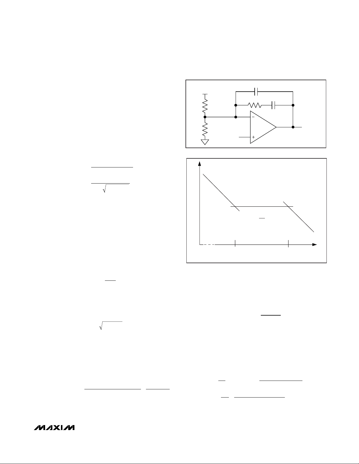
Oscillator
Use an external resistor at RT to program the
MAX15022 switching frequency from 500kHz to 4MHz.
Calculate the appropriate resistor value at RT for the
desired output switching frequency (fSW):
Tracking/Sequencing
The MAX15022 features coincident/ratiometric tracking
and sequencing (see Figure 1). Connect SEL to ground
to configure the device as a sequencer. Connect SEL to
AVIN for tracking with output 1 as the master. Leave SEL
unconnected for tracking with output 2 as the master.
Assign the output with the higher voltage as the master.
Figure 1. Graphical Representation of Coincident Tracking,
Ratiometric Tracking, and Sequencing
067
.
Rk
[]
T
f [kHz] 1 [V]
SW
Ω=
32 μ
A
[]
×
×
4[MHz]
V
OUT1
V
OUT2
SOFT-START
a) COINCIDENT TRACKING OUTPUTS
V
OUT1
V
OUT2
SOFT-START
b) RATIOMETRIC TRACKING OUTPUTS
V
OUT1
V
OUT2
SOFT-START
c) SEQUENCED OUTPUTS
SOFT-STOP
SOFT-STOP
SOFT-STOP
Page 13
MAX15022
Dual, 4A/2A, 4MHz, Step-Down DC-DC
Regulator with Dual LDO Controllers
______________________________________________________________________________________ 13
Coincident/Ratiometric Tracking
The enable inputs in conjunction with digital soft-start
and soft-stop provide coincident/ratiometric tracking.
Track an output voltage by connecting a resistive
divider from the output being tracked to its enable
input. For example, for V
OUT2
to coincidentally track
V
OUT1
, connect the same resistive divider used for
FB2, from V
OUT1
to EN2 to SGND (see Figure 2).
Track ratiometrically by connecting EN_ to SGND. This
synchonizes the soft-start and soft-stop of all the regulator references, and hence their respective output voltages will track ratiometrically (see Figure 2).
When the MAX15022 regulators are configured as voltage trackers, output short-circuit fault conditions at
either master or slave output are handled carefully—neither the master nor slave output will remain energized
when the other output is shorted to ground. When the
slave is shorted and enters into hiccup mode, the master will soft-stop. When the master is shorted and the
part enters into hiccup mode, the slave will ratiometrically soft-stop. Coming out of hiccup mode, both outputs
will soft-start coincidently or ratiometrically depending
on their initial configuration. During the thermal shutdown or power-off when the input falls below its UVLO,
the output voltages track down depending on the
respective output capacitance and load.
See Figure 1 for a graphical representation of coincident/ratiometric tracking.
Sequencing
When sequencing, the voltage at the enable inputs
must exceed 1.225V (typ) for each PWM controller to
start (see Figure 1c).
Figure 2. Ratiometric Tracking and Coincident Tracking Configurations
a) b)
RATIOMETRIC TRACKING
V
PVIN1
EN1
COINCIDENT TRACKING
V
PVIN1
EN1
c)
COINCIDENT TRACKING
V
PVIN2
EN2
V
EN2
SEL AVIN
OUTPUT 1 IS THE MASTER AND
OUTPUT 2 IS THE SLAVE.
V
PVIN2
EN2
EN1
SEL UNCONNECTED
OUTPUT 2 IS THE MASTER AND
OUTPUT 1 IS THE SLAVE.
OUT1
EN2
V
OUT2
FB2
SEL
OUTPUT 1 IS THE MASTER AND
OUTPUT 2 IS THE SLAVE.
R
R
R
R
AVIN
V
OUT2
A
EN1
B
V
OUT1
A
FB1
B
SEL
OUTPUT 2 IS THE MASTER AND
OUTPUT 1 IS THE SLAVE.
R
C
R
D
R
C
R
D
UNCONNECTED
Page 14

MAX15022
Dual, 4A/2A, 4MHz, Step-Down DC-DC
Regulator with Dual LDO Controllers
14 ______________________________________________________________________________________
Error Amplifier
The output of the internal voltage-mode error amplifier
(COMP_) is provided for frequency compensation (see
the
Compensation Design Guidelines
section). FB_ is
the inverting input of the error amplifier. The error
amplifier has an 80dB open-loop gain and a 12MHz
gain bandwidth (GBW) product.
Output Short-Circuit
Protection (Hiccup Mode)
The MAX15022 features lossless, high-side peak current limit and low-side, valley current limit. At short duty
cycles, both limits are active. At high duty cycles, only
the high-side peak current limit is active. Either limit
causes the hiccup mode counter (NCL) to increment.
For duty cycles less than 50%, the low-side valley current limit is active. Once the high-side MOSFET turns off,
the voltage across the low-side MOSFET is monitored. If
this voltage does not exceed the current-limit threshold
at the end of the cycle, the high-side MOSFET turns on
normally at the start of the next cycle. If the voltage
exceeds the current-limit threshold just before the
beginning of a new PWM cycle, the controller skips that
cycle. During severe overload or short-circuit conditions, the switching frequency of the device appears to
decrease because the on-time of the low-side MOSFET
extends beyond a clock cycle.
If the current-limit threshold is exceeded for more than
four cumulative clock cycles (NCL), the device shuts
down for 8192 clock cycles (hiccup timeout) and then
restarts with a soft-start sequence. If three consecutive
cycles pass without a current-limit event, the count of
NCLis cleared (see Figure 3). Hiccup mode protects
the device against a continuous output short circuit.
The internal current limit is constant from 5.5V down to
3V and decreases linearly by 50% from 3V to 2V. See
the
Electrical Characteristics
table.
Thermal-Overload Protection
The MAX15022 features an integrated thermal-overload
protection with temperature hysteresis. Thermal-overload protection limits the die temperature of the device
and protects it in the event of an extended thermal fault
condition. When the die temperature exceeds +160°C,
an internal thermal sensor shuts down the device, turning off the internal power MOSFETs and allowing the die
to cool. After the die temperature falls by +15°C (typ),
the device restarts with a soft-start sequence.
Startup into a Prebiased Output
(Sequencing Mode)
In sequencing mode, the regulators start with minimal
glitch into a prebiased output and soft-stop is disabled.
During soft-start, both switches are kept off until the
PWM comparator commands its first PWM pulse. Until
then, the converters do not sink current from the outputs. The first PWM pulse occurs when the ramping reference voltage increases above the FB_ voltage.
LDO Controllers
The MAX15022 provides two additional LDO controllers
to drive external PNP pass transistors. Connect the emitter of each PNP pass transistor to either the input supply
or one of the controller 1 or 2 outputs. Each LDO controller features an independent enable input and digital
soft-start. Connect FB3 and FB4 to the center tap of a
resistive divider from the output of the desired LDO controller to SGND to set the output voltage.
PWM Controllers
Design Procedure
Setting the Switching Frequency
Connect a 4.2kΩ to 33kΩ resistor from RT to SGND to
program the switching frequency (fSW) from 500kHz to
4MHz. Calculate the required resistor value RRTto set
the switching frequency with the following equation:
Higher frequencies allow designs with lower inductor
values and less output capacitance. At higher switching frequencies core losses, gate-charge currents,
and switching losses increase. When operating from
V
AVIN
< 3V, the fSWfrequency should be derated to
3MHz (maximum).
Figure 3. Hiccup-Mode Block Diagram
CURRENT LIMIT
IN
CLR
IN
CLR
R
[]
kAΩ=
RT
COUNT OF 4
N
CL
COUNT OF 3
N
CLR
INITIATE HICCUP
TIMEOUT
f [kHz] 1 [V]
SW
32 4[MHz]
[]
μ
.
××067
N
HT
Page 15

MAX15022
Dual, 4A/2A, 4MHz, Step-Down DC-DC
Regulator with Dual LDO Controllers
______________________________________________________________________________________ 15
Effective Input-Voltage Range
Although the MAX15022’s regulators can operate from
input supplies ranging from 2.5V to 5.5V, the input-voltage range can be effectively limited by the
MAX15022’s duty-cycle limitations for a given output
voltage (V
OUT_
). The maximum input voltage
(V
PVIN_MAX
) can be effectively limited by the control-
lable minimum on-time (t
ON(MIN)
):
where t
ON(MIN)
is 0.06μs (typ).
The minimum input voltage (V
PVIN_MIN
) can be effectively limited by the maximum controllable duty cycle
and is calculated using the following equation:
where V
OUT_
is the regulator output voltage and
t
OFF(MIN)
is the 0.06μs (typ) controllable off-time.
Inductor Selection
Three key inductor parameters must be specified for
operation with the MAX15022: inductance value (L),
peak inductor current (I
PEAK
), and inductor saturation
current (I
SAT
). The minimum required inductance is a
function of operating frequency, input-to-output voltage
differential, and the peak-to-peak inductor current
(ΔI
P-P
). Higher ΔI
P-P
allows for a lower inductor value. A
lower inductance minimizes size and cost and
improves large-signal and transient response.
However, efficiency is reduced due to higher peak currents and higher peak-to-peak output-voltage ripple for
the same output capacitor. A higher inductance
increases efficiency by reducing the ripple current;
however, resistive losses due to extra wire turns can
exceed the benefit gained from lower ripple current levels especially when the inductance is increased without
also allowing for larger inductor dimensions. Choose
the inductor’s peak-to-peak current, ΔI
P-P,
in the range
of 20% to 50% of the full load current; as a rule of
thumb 30% is typical.
Calculate the inductance, L, using the following equation:
where V
PVIN_
is the input supply voltage, V
OUT_
is the
regulator output voltage, and fSWis the switching frequency. Use typical values for V
PVIN_
and V
OUT_
so
that efficiency is optimum for typical conditions. The
switching frequency (fSW) is programmable between
500kHz and 4MHz (see the
Oscillator
section).
The peak-to-peak inductor current (ΔI
P-P
), which
reflects the peak-to-peak output ripple, is largest at the
maximum input voltage. See the
Output-Capacitor
Selection
section to verify that the worst-case output
current ripple is acceptable.
Select an inductor with a saturation current, I
SAT
, higher than the maximum peak current to avoid runaway
current during continuous output short-circuit conditions. Also, confirm that the inductor’s thermal performances and projected temperature rise above ambient
does not exceed its thermal capacity. Many inductor
manufacturers provide bias/load current versus temperature rise performance curves (or similar) to obtain
this information.
Input-Capacitor Selection
The discontinuous input current of the buck converter
causes large input ripple currents and therefore the
input capacitor must be carefully chosen to withstand
the input ripple current and keep the input-voltage ripple within design requirements.
The input-voltage ripple is comprised of ΔVQ(caused
by the capacitor discharge) and ΔV
ESR
(caused by the
ESR of the input capacitor). The total voltage ripple is
the sum of ΔVQand ΔV
ESR
which peaks at the end of
the on-cycle. Calculate the required input capacitance
and ESR for a specified ripple using the following equations:
I
LOAD(MAX)
is the maximum output current, ΔI
P-P
is the
peak-to-peak inductor current, and V
PVIN_
is the input
supply voltage, V
OUT_
is the regulator output voltage,
and fSWis the switching frequency.
V [V]
PVIN_MAX
≤
t [ s] f [MHz]
V [V]
OUT_
ON(MIN) SW
×μ
V [V]
V [V]
PVIN_MIN
≥
1 (t [ s] f [MHz])
−×μ
OFF(MIN) SW
OUT_
V [V] (V [V] V [V])
LH
[]
μ=
OUT_ PVIN_ OUT_
V [V] f [MHz]
PVIN_ SW
×−
××
IA
Δ
PP
−
[]
V [mV]
Δ
ESR
V [V] f [MHz]
Δ
×
QSW
−
××
C
Δ
ESR
[]
m
Ω
=
⎛
I
⎜
LOAD(MAX)
⎝
I [A]
LOAD(MAX)
[]
F
μ
PVIN_
I [A]
−
PP
=
V V [V] V [V]
()
PVIN_ OUT_ OUT_
=
V [V] f [MHz] L
PVIN_ SW
I
Δ
−
PP
+
2
⎛
V [V]
OUT_
×
⎜
V [V]
⎝
PVIN_
×
⎞
[A]
⎟
⎠
⎞
⎟
⎠
[]
H
μ
Page 16

MAX15022
Dual, 4A/2A, 4MHz, Step-Down DC-DC
Regulator with Dual LDO Controllers
16 ______________________________________________________________________________________
Use the following equation to calculate the input ripple
when only one regulator is enabled:
The MAX15022 includes UVLO hysteresis to avoid possible unintentional chattering during turn-on. Use additional
bulk capacitance if the input source impedance is high. If
using a lower input voltage, additional input capacitance
helps to avoid possible undershoot below the undervoltage lockout threshold during transient loading.
Output-Capacitor Selection
The allowed output-voltage ripple and the maximum
deviation of the output voltage during load steps determine the required output capacitance and its ESR. The
output ripple is mainly composed of ΔVQ(caused by
the capacitor discharge) and ΔV
ESR
(caused by the
voltage drop across the equivalent series resistance of
the output capacitor). The equations for calculating the
output capacitance and its ESR are:
where ΔI
P-P
is the peak-to-peak inductor current, and
fSWis the switching frequency.
ΔV
ESR
and ΔVQare not directly additive since they are
out of phase from each other. If using ceramic capacitors, which generally have low ESR, ΔVQ dominates. If
using electrolytic capacitors, ΔV
ESR
dominates.
The allowable deviation of the output voltage during
fast load transients also affects the output capacitance,
its ESR, and its equivalent series inductance (ESL). The
output capacitor supplies the load current during a
load step until the controller responds with an
increased duty cycle. The response time (t
RESPONSE
)
depends on the gain bandwidth of the controller (see
the
Compensation-Design Guidelines
section). The
resistive drop across the output capacitor’s ESR
(ΔV
ESR
), the drop across the capacitor’s ESL (ΔV
ESL
),
and the capacitor discharge (ΔVQ) causes a voltage
droop during the load-step (I
STEP
). Use a combination
of low-ESR tantalum/aluminum electrolyte and ceramic
capacitors for better load transient and voltage ripple
performance. Non-leaded capacitors and capacitors in
parallel help reduce the ESL. Keep the maximum out-
put-voltage deviation below the tolerable limits of the
electronics being powered.
Use the following equations to calculate the required
output capacitance, ESR, and ESL for minimal output
deviation during a load step:
where I
STEP
is the load step, t
STEP
is the rise time of the
load step, and t
RESPONSE
is the response time of the
controller.
Compensation Design Guidelines
The MAX15022 uses a fixed-frequency, voltage-mode
control scheme that regulates the output voltage by
comparing the output voltage against a fixed reference.
The subsequent “error” voltage that appears at the
error-amplifier output (COMP_) is compared against an
internal ramp voltage to generate the required duty
cycle of the PWM. A second order lowpass LC filter
removes the switching harmonics and passes the DC
component of the PWM signal to the output. The LC filter has an attenuation slope of -40dB/decade and introduces 180° of phase shift at frequencies above the LC
resonant frequency. This phase shift in addition to the
inherent 180° of phase shift of the regulator’s negative
feedback system turns the feedback into unstable positive feedback. The error amplifier and its associated
circuitry must be designed to achieve a stable closedloop system.
The basic controller loop consists of a power modulator
(comprised of the regulator’s PWM, associated circuitry,
and LC filter), an output feedback divider, and an error
amplifier. The power modulator has a DC gain set by
V
AVIN/VRAMP
where the ramp voltage (V
RAMP
) is a func-
tion of the V
AVIN
and results in a fixed DC gain of 4V/V,
providing effective feed-forward compensation of inputvoltage supply DC variations. The feed-forward compensation eliminates the dependency of the power modulator’s gain on the input voltage such that the feedback
compensation of the error amplifier requires no modifications for nominal input-voltage changes. The output
filter is effectively modeled as a double-pole and a single zero set by the output inductance (L), the DC resistance of the inductor (DCR), the output capacitance
(C
OUT
), and its equivalent series resistance (ESR).
I [A] I [A]
CIN(RMS) LOAD(MAX)
=×
V [V] V V [V]
OUT_ PVIN_ OUT_
×−
()
V [V]
PVIN_
I [A]
Δ
PP
Δ
QSW
2 V [mV]
×
Δ
I [A]
Δ
PP
CF
[]
μ=
OUT
ESR m
8 V [V] f [MHz]
××
=
Ω
[]
−
ESR
−
V [mV]
Δ
ESR
=
I [A]
STEP
×
V [V]
Δ
Q
ESL STEP
×
I [A]
STEP
C
OUT
ESL
ESR m
[]
Ω
I [A] t
STEP RESPONSE
[]
μ
F
=
V [mV] t
Δ
[]
nH
=
[]
μ
s
[]
s
μ
Page 17
MAX15022
Dual, 4A/2A, 4MHz, Step-Down DC-DC
Regulator with Dual LDO Controllers
______________________________________________________________________________________ 17
Below are equations that define the power modulator:
R
OUT
is the load resistance of the regulator, fLCis the
resonant break frequency of the filter, and f
ESR
is the
ESR zero of the output capacitor. See the
Closed-Loop
Response and Compensation of Voltage-Mode
Regulators
for more information on fLCand f
ESR
.
The switching frequency (fSW) is programmable
between 500kHz and 4MHz. Typically, the crossover
frequency (fCO)—the frequency at which the system’s
closed-loop gain is equal to unity (crosses 0dB)—
should be set at or below one-tenth the switching frequency (fSW/10) for stable closed-loop response.
The MAX15022 provides an internal voltage-mode error
amplifier with its inverting input and its output available to
the user for external frequency compensation. The flexibility of external compensation for each controller offers
a wide selection of output filtering components, especially the output capacitor. For cost-sensitive applications,
use aluminum electrolytic capacitors while for spacesensitive applications, use low-ESR tantalum or multilayer ceramic chip (MLCC) capacitors at the output. The
higher switching frequencies of the MAX15022 allow the
use of MLCC as the primary filter capacitor(s).
First, select the passive and active power components
that meet the application output ripple, component
size, and component cost requirements. Second,
choose the small-signal compensation components to
achieve the desired closed-loop frequency response
and phase margin as outlined below.
Closed-Loop Response and Compensation
of Voltage-Mode Regulators
The power modulator’s LC lowpass filter exhibits a variety of responses, dependent on the value of the L and
C and their parasitics. Higher resistive parasitics
reduce the Q of the circuit, reducing the peak gain and
phase of the system; however, efficiency is also
reduced under these circumstances.
One such response is shown in Figure 4a. In this example, the ESR zero occurs relatively close to the filter’s
resonant break frequency, fLC. As a result, the power
modulator’s uncompensated crossover is approximately one third the desired crossover frequency, fCO. Note
also, the uncompensated rolloff through the 0dB plane
follows a single-pole, -20dB/decade slope and 90° of
phase lag. In this instance, the inherent phase margin
ensures a stable system; however, the gain-bandwidth
product is not optimized.
Figure 4a. Power Modulator Gain and Phase Response with
Lossy Bulk Output Capacitor(s) (Aluminum)
Figure 4b. Power Modulator and Type II Compensator Gain and
Phase Response with Lossy Bulk Output Capacitor(s) (Aluminum)
Gain
MOD(DC)
V
AVIN
===
V
RAMP
V
AVIN
V
AVIN
4V/V
4
1
2LC
××
π
OUT
OUT
f
ESR
1
⎛
R ESR
OUT
⎜
R DCR
⎝
OUT
=
2 ESR C
××
π
≈
⎞
+
⎟
+
⎠
1
OUT
f
=
LC
2LC
×× ×
π
40
20
|G
MOD
0
-20
MAGNITUDE (dB)
-40
-60
-80
10
f
LC
| ASYMPTOTE
< G
MOD
100 1k 10k
FREQUENCY (Hz)
MAX15022 fig04a
|G
MOD
f
ESR
100k
|
1M 10M
90
45
0
-45
PHASE (DEGREES)
-90
-135
-180
|G
MOD
MAX15022 fig04b
f
CO
|
1M 10M
180
135
90
45
0
-45
PHASE (DEGREES)
-90
-135
-180
80
60
40
|GEA|
20
0
-20
MAGNITUDE (dB)
-40
-60
-80
10
<G
EA
f
LC
f
< G
MOD
100 1k 10k 100k
ESR
FREQUENCY (Hz)
Page 18
MAX15022
Dual, 4A/2A, 4MHz, Step-Down DC-DC
Regulator with Dual LDO Controllers
18 ______________________________________________________________________________________
As seen in Figure 4b, a Type II compensator provides for
stable closed-loop operation, leveraging the +20dB/
decade slope of the capacitor’s ESR zero, while extending the closed-loop gain bandwidth of the regulator. The
zero crossover now occurs at approximately three times
the uncompensated crossover frequency, f
CO
.
The Type II compensator’s midfrequency gain (approximately 12dB shown here) is designed to compensate
for the power modulator’s attenuation at the desired
crossover frequency, f
CO
(Gain
E/A
+ Gain
MOD
= 0dB at
fCO). In this example, the power modulator’s inherent
-20dB/decade rolloff above the ESR zero (f
ZERO, ESR
)
is leveraged to extend the active regulation gain bandwidth of the voltage regulator. As shown in Figure 4b,
the net result is a three times increase in the regulator’s
gain bandwidth while providing greater than 75° of
phase margin (the difference between Gain
E/A
and
Gain
MOD
respective phases at crossover, fCO).
Other filter schemes pose their own problems. For
instance, when choosing high-quality filter capacitor(s),
e.g. MLCCs, the inherent ESR zero may occur at a
much higher frequency, as shown in Figure 4c.
As with the previous example, the actual gain and
phase response is overlaid on the power modulator’s
asymptotic gain response. One readily observes the
more dramatic gain and phase transition at or near the
power modulator’s resonant frequency, fLC, versus the
gentler response of the previous example. This is due
to the filter components’ lower parasitic (DCR and ESR)
and corresponding higher frequency of the inherent
ESR zero. In this example, the desired crossover frequency occurs below the ESR zero frequency.
In this example, a compensator with an inherent midfrequency double-zero response is required to mitigate
the effects of the filter’s double-pole phase lag. This is
available with the Type III topology.
As demonstrated in Figure 4d, the Type III’s midfrequency double-zero gain (exhibiting a +20dB/decade
slope, noting the compensator’s pole at the origin) is
designed to compensate for the power modulator’s
double-pole -40dB/decade attenuation at the desired
crossover frequency, fCO(again, Gain
E/A
+ Gain
MOD
=
0dB at fCO) (see Figure 4d).
In the above example, the power modulator’s inherent
(midfrequency) -40dB/decade rolloff is mitigated by the
midfrequency double zero’s +20dB/decade gain to
extend the active regulation gain bandwidth of the voltage regulator. As shown in Figure 4d, the net result is
an approximate doubling in the controller’s gain bandwidth while providing greater than 55° of phase margin
(the difference between Gain
E/A
and Gain
MOD
respec-
tive phases at crossover, fCO).
Design procedures for both Type II and Type III compensators are shown below.
Figure 4c. Power Modulator Gain and Phase Response with
Low-Parasitic Capacitor(s) (MLCCs)
Figure 4d. Power Modulator and Type III Compensator Gain
and Phase Response with Low Parasitic Capacitors (MLCCs)
40
|G
|
20
0
-20
MAGNITUDE (dB)
-40
-60
-80
10
MOD
< G
MOD
|G
|
MOD
ASYMPTOTE
100 1k 10k 100k
FREQUENCY (Hz)
MAX15022 fig04c
f
LC
1M 10M
90
45
0
f
ESR
-45
PHASE (DEGREES)
-90
-135
-180
80
60
40
|GEA|
20
0
-20
MAGNITUDE (dB)
-40
-60
-80
10
< G
EA
f
LC
< G
MOD
100 1k 10k 100k
FREQUENCY (Hz)
MAX15022 fig04d
f
CO
|G
MOD
f
ESR
1M 10M
270
203
135
68
0
|
-68
-135
-203
-270
PHASE (DEGREES)
Page 19
MAX15022
Dual, 4A/2A, 4MHz, Step-Down DC-DC
Regulator with Dual LDO Controllers
______________________________________________________________________________________ 19
Type II: Compensation when fCO> f
ZERO, ESR
When the f
CO
is greater than f
ESR
, a Type II compensation network provides the necessary closed-loop compensated response. The Type II compensation network
provides a midband compensating zero and a high-frequency pole (see Figures 5a and 5b).
RFCF provides the midband zero f
MID,ZERO
, and
RFC
CF
provides the high-frequency pole, f
HIGH,POLE
.
Use the following procedure to calculate the compensation network components.
Calculate the f
ESR
and LC double pole, fLC:
where C
OUT
is the regulator output capacitor and ESR
is the series resistance of C
OUT
. See the
Output-
Capacitor Selection
section for more information on cal-
culating C
OUT
and ESR.
Set the compensator’s leading zero, fZ1, at or below the
filter’s resonant double-pole frequency from:
Set the compensator’s high-frequency pole, f
P1
, at or
below one-half the switching frequency, f
SW
:
To maximize the compensator’s phase lead, set the
desired crossover frequency, fCO, equal to the geometric mean of the compensator’s leading zero, fZ1, and
high-frequency pole, fP1, as follows:
Select the feedback resistor, RF, in the range of 3.3kΩ
to 30kΩ.
Calculate the gain of the modulator (Gain
MOD
)—comprised of the regulator’s PWM, LC filter, feedback divider,
and associated circuitry—at the desired crossover frequency, f
CO
, using the following equation:
where VFBis the 0.6V (typ) FB_ input-voltage set-point,
L is the value of the regulator inductor, ESR is the
series resistance of the output capacitor, and V
OUT_
is
the desired output voltage.
The gain of the error amplifier (Gain
E/A
) in the midband
frequencies is:
The total loop gain is the product of the modulator gain
and the error amplifier gain at f
CO
and should be set
equal to 1 as follows:
Gain
MOD
x Gain
E/A
= 1
So:
Figure 5a. Type II Compensation Network
Figure 5b. Type II Compensation Network Response
f
ESR
f
LC
=
≈
2 ESR C
2LC
1
××
π
1
××
π
OUT
OUT
ff
≤
Z1 LC
f
SW
f
≤
P1
2
fff
=×
CO Z1 P1
Gain 4(V/V)
=×
MOD
ESR [m ]
2 f [kHz] L[ H]
××
πμ
()
CO
Ω
V [V]
FB
×
V [V]
OUT_
C
2ND ASYMPTOTE
-1
)
CF
C
R
F
F
-1
R
F
)
(
R
I
3RD ASYMPTOTE
(ωR
FCCF
2ND POLE
(R
FCCF
V
OUT_
R
1
FB_
R
2
V
REF
GAIN
(dB)
1ST ASYMPTOTE
-1
)
(ωR
1CF
1ST POLE
(AT ORIGIN)
1ST ZERO
(R
FCF
R [k ]
Ω
Gain
E/A
=
R [k ]
F
Ω
1
⎤
⎡
R
F
⎥
10
⎢
R
1
⎦
⎣
R
F
×
R
2 f L x V
π
1
20 log 20 log 0dB
×+× =
⎡
4 ESR x V
⎢
π
××
2 f L x V
10
⎢
⎣
4 ESR x V
×
××
CO OUT_
×
CO OUT_
FB
FB
1
=
COMP_
-1
)
ω (rad/sec)
-1
)
⎤
⎥
⎥
⎦
Page 20
MAX15022
Dual, 4A/2A, 4MHz, Step-Down DC-DC
Regulator with Dual LDO Controllers
20 ______________________________________________________________________________________
Solving for R1:
where VFBis the 0.6V (typ) FB_ input-voltage set-point,
L is the value of the regulator inductor, ESR is the
series resistance of the output capacitor, and V
OUT_
is
the desired output voltage.
1) CFis determined from the compensator’s leading
zero, fZ1, and RFas follows:
2) C
CF
is determined from the compensator’s high-fre-
quency pole, f
P1
, and RFas follows:
3) Calculate R2using the following equation:
where VFB= 0.6V (typ) and V
OUT_
is the output voltage
of the regulator.
Type III: Compensation when f
CO
< f
ESR
As indicated above, the position of the output capacitor’s inherent ESR zero is critical in designing an appropriate compensation network. When low-ESR ceramic
output capacitors (MLCCs) are used, the ESR zero frequency (f
ESR
) is usually much higher than the desired
crossover frequency (fCO). In this case, a Type III compensation network is recommended (see Figure 6a).
As shown in Figure 6b, the Type III compensation network introduces two zeros and three poles into the control loop. The error amplifier has a low-frequency pole
at the origin, two zeros, and two higher frequency poles
at the following frequencies:
Two midband zeros (f
Z1
and fZ2) are designed to compensate for the pair of complex poles introduced by the
LC filter.
f
P1
introduces a pole at zero frequency (integrator) for
nulling DC output-voltage errors.
fP1= at the origin (0Hz)
Depending on the location of the ESR zero (f
ESR
), f
P2
can be used to cancel it, or to provide additional attenuation of the high-frequency output ripple.
fP3attenuates the high-frequency output ripple.
Since CCF<< CFthen:
Figure 6a. Type III Compensation Network
Figure 6b. Type III Compensation Network Response
V
R [k ] 4 ESR[m ] V [V]
ΩΩ
×× ×
R [k ]
Ω
1
FFB
=
2 f [kHz] L[ H] V [V]
×××πμ
CO OUT_
C[F]
μπ=
F
××Ω
2 R [k ] f [kHz]
1
FZ1
R
I
C
I
GAIN
(dB)
OUT_
R
1
FB_
R
2
V
REF
C
CF
C
R
F
F
COMP_
CF]
[μπ=
CF
××Ω
2 R [k ] f [kHz]
1
FP1
V [V]
R[k] R[k]
ΩΩ=×
21
FB
V [V] V [V]
OUT_ FB
−
f
f
Z2
=
Z1
=
2C(RR)
1
××
π
2RC
FF
1
×× +
π
I1I
1ST ASYMPTOTE
-1
)
(ωR
ICF
2ND ASYMPTOTE
1ST POLE
(AT ORIGIN)
(
1ST ZERO
)
(R
FCF
-1
R
F
)
R
1
-1
2ND ZERO
(R
1CI
4TH ASYMPTOTE
3RD ASYMPTOTE
(ωR
FCI
2ND POLE
-1
)
(R
ICI
-1
)
R
F
)
(
R
I
5TH ASYMPTOTE
-1
)
(R
FCCF
-1
)
ICCF
ω (rad/sec)
-1
)
3RD POLE
(R
f
P2
1
=
××π
2RC
II
f
=
P3
π
2R CC
××
1
()
FFCF
=
π
2R
1
CC
××
F
CC
×
FCF
+
FCF
f
=
P3
1
××π
2 R C
FCF
Page 21

MAX15022
Dual, 4A/2A, 4MHz, Step-Down DC-DC
Regulator with Dual LDO Controllers
______________________________________________________________________________________ 21
The locations of the zeros and poles should be such
that the phase margin peaks around fCO.
Set the ratios of fCO-to-fZand fP-to-fCOequal to one another, e.g.,
fCO= f
P = 5 is a good number to get approximately
fZf
CO
60° of phase margin at fCO. Whichever technique, it is
important to place the two zeros at or below the double
pole to avoid the conditional stability issue.
The following procedure is recommended:
1) Select a crossover frequency, fCO, at or below one-
tenth the switching frequency (f
SW
):
2) Calculate the LC double-pole frequency, fLC:
where C
OUT
is the output capacitor of the regulator.
3) Select the feedback resistor, RF, in the range of
3.3kΩ to 30kΩ.
4) Place the compensator’s first zero
at or below the output filter’s double-pole, fLC, as follows:
5) The gain of the modulator (Gain
MOD
)—comprised of
the regulator’s PWM, LC filter, feedback divider, and
associated circuitry—at the crossover frequency is:
The gain of the error amplifier (Gain
E/A
) in midband fre-
quencies is:
The total loop gain is the product of the modulator gain
and the error amplifier gain at f
CO
should be equal to 1,
as follows:
Gain
MOD
x Gain
E/A
= 1
So:
Solving for CI:
6) For those situations where fLC< fCO< f
ESR
< fSW/2,
as with low-ESR tantalum capacitors, the compensator’s second pole (fP2) should be used to cancel
f
ESR
. This provides additional phase margin. On the
system Bode plot, the loop gain maintains its
+20dB/decade slope up to 1/2 of the switching frequency verses flattening out soon after the 0dB
crossover. Then set:
f
P2
= f
ESR
If a ceramic capacitor is used, then the capacitor ESR
zero, f
ESR
, is likely to be located even above 1/2 of the
switching frequency, that is fLC< fCO< fSW/2 < f
ESR
. In
this case, the frequency of the second pole (fP2) should
be placed high enough not to significantly erode the
phase margin at the crossover frequency. For example,
fP2can be set at 5 x fCO, so that its contribution to phase
loss at the crossover frequency f
CO
is only about 11°:
f
P2
= 5 x f
CO
Once fP2is known, calculate RI:
7) Place the second zero (fZ2) at 0.2 x fCOor at fLC,
whichever is lower, and calculate R1using the following equation:
8) Place the third pole (fP3) at 1/2 the switching fre-
quency and calculate C
CF
from:
9) Calculate R
2
as:
where V
FB
= 0.6V (typ).
f [kHz]
f [kHz]
CO
SW
≤
10
1
OUT
f [MHz]
LC
≈
2 L[ H] C F]
××πμ μ[
f
=
Z1
1
××π
2RC
FF
C[F]
μπ=
F
×××Ω
2 R [k ] 0.5 f [kHz]
1
FLC
Gain 4
MOD
=×
(2 f [MHz]) L[ H] C [ F]
×××πμμ
CO
1
2
OUT
Gain 2 f [kHz] C [ F] R [k ]
=× × ×πμΩ
E/A CO I F
2 f [kHz] L[ H] C [ F]
×××
πμμ
()
C pF]
[ =
I
CO OUT
4 R [k ]
×
Ω
F
R[k ]
Ω=
I
××πμ
2 f [kHz] C [ F]
1
P2 I
R[k ]
Ω=
1
2 f [kHz] C [ F]
1
××πμ
Z2 I
C[F]
n =
CF
πΩ
2 0.5 f [MHz] R [k ]
×× ×
()
1
SW F
4
×
(2 f [kHz]) C [ F] L[ H]
×××
πμμ
CO
2 f [kHz] C [ F] R [k ] 1
×× × × =
π pΩ
CO I F
1
2
OUT
R[k] R[k]
21
ΩΩ=×
V [V] V [V]
OUT_ FB
V [V]
FB
−
Page 22

MAX15022
Dual, 4A/2A, 4MHz, Step-Down DC-DC
Regulator with Dual LDO Controllers
22 ______________________________________________________________________________________
LDO Controllers
Design Procedure
PNP Pass Transistors Selection
The pass transistors must meet specifications for current
gain (ß), input capacitance, collector-emitter saturation
voltage, and power dissipation. The transistor’s current
gain limits the guaranteed maximum output current to:
where I
B3/4(MIN)
is the minimum base-drive current and
R
PULL
is the pullup resistor connected between the
transistor’s base and emitter.
In addition, to avoid premature dropout, V
CE-SAT
must
be less than or equal to (V
PVIN_(MIN)
- V
OUT3/4
).
Furthermore, the transistor’s current gain increases the
linear regulator’s DC loop gain (see the
Stability
Requirements
section), so excessive gain destabilizes
the output. Therefore, transistors with high current gain
at the maximum output current, such as Darlington
transistors, are not recommended. The transistor’s
input capacitance and input resistance also create a
second pole, which could be low enough to destabilize
the LDO when the output is heavily loaded.
The transistor’s saturation voltage at the maximum output current determines the minimum input-to-output voltage differential that the linear regulator supports.
Alternately, the package’s power dissipation could limit
the useable maximum input-to-output voltage differential.
The maximum power-dissipation capability of the transistor’s package and mounting must support the actual
power dissipation in the device without exceeding the
maximum junction temperature. The power dissipated
equals the maximum load current multiplied by the
maximum input-to-output voltage differential.
Output 3 and Output 4 Voltage Selection
The MAX15022 positive linear-regulator output voltage
is set with a resistive divider from the desired output
(V
OUT3/4
) to FB3/4 to SGND (see Figures 7 and 8).
First, select the R
2FB3/4
resistance value (below 30kΩ).
Then, solve for R
1FB3/4
:
where V
OUT3/4
can support output voltages as low as
0.6V and V
FB3/4
is 0.6V (typ).
Stability Requirements
The MAX15022’s B3 and B4 outputs are designed to
drive bipolar PNP transistors. These PNP transistors
form linear regulators with positive outputs. An internal
transconductance amplifier drives the external pass
transistors. The transconductance amplifier, pass transistor’s specifications, the base-emitter resistor, and the
output capacitor determine the loop stability.
The total DC loop gain (A
V
) is the product of the gains of
the internal transconductance amplifier, the gain from
base to collector of the pass transistor, and the attenuation of the feedback divider. The transconductance amplifier regulates the output voltage by controlling the pass
transistor’s base current. Its DC gain is approximately:
where gC_is the transconductance of the internal
amplifier and is typically 1.2mA/mV, R
P1/2
is the resistor
across the base and the emitter of the pass transistor in
kΩ, and RINis the input resistance of the pass transistor, and can be calculated by:
The DC gain for the pass transistor (AP), including the
feedback divider, is approximately:
The total DC loop gain for output 3 and output 4 is:
The output capacitance (C
OUT_
) and the load resis-
tance (R
OUT_
) create a dominant pole (f
POLE1
) at:
I [A] I [A]
OUT3/4 B3/4(MIN)
⎛
=
⎜
⎝
−
R
V [V]
BE
PULL
⎞
⎟
[]Ω
⎠
×
β
g
R
[]
IN
Ag
=×
PmPNP
−
R
2FB3/4
RR
1FB3/4 2F
ImA
OUT3/4
=
where g
×
mPNP
−
⎛
RR
×
IN P1/2
×
C_
⎜
RR
+
⎝
IN P1/2
⎛
kx
Ω=
β
⎜
I
⎝
OUT3/4
⎡
R(RR)
OUT3/4 1FB3/4 2FB3/4
⎢
R
⎣
+
26 mV
×+
OUT3/4
+
BB3/4
[]
.
[]
⎞
⎟
⎠
26[mV]
[]
A
μ
RRR
+
1FB3/4 2FB3/4
⎞
⎟
⎠
⎤
⎥
⎦
RR
[] []kkΩΩ=
1FB3/4 2FB3/4
⎛
⎜
⎝
V [V]
OUT3/4
V [V]
FB3/4
⎞
1
−
⎟
⎠
⎛
RR
×
Ag
=×
VC_
f [kHz]
POLE1
=
2C R
πμ
=
2 C V [V]
πμ
IN P1/2
⎜
RR
+
⎝
IN P1/2
1
××
××
[] []
OUT3/4 OUT3/4
I [mA]
OUT3/4(MAX)
OUT3/4 OUT3/4
Fk
[]
F
⎞
×
⎟
⎠
A
P
Ω
Page 23

The input capacitance to the base of the pass transistor
(C
QIN
), any external base-to-emitter capacitance (CBE,
see the
Base-Drive Noise Reduction
section), the transistor’s input resistance (RIN), and the base-to-emitter
pullup resistor (RP_) set a second pole:
To maintain the stability, at a minimum the following
condition must be satisfied:
i.e., the second pole must occur above the unity-gain
crossover. At heavy output load, we can simplify as follows:
And hence, the output capacitance (C
OUT3/4
) must sat-
isfy the following equation:
where:
ß is the current gain of the PNP transistor, gC_is the
transconductance of the internal amplifier (1.2mA/mV
typical), and τFis the forward transit time of the PNP
transistor. For example, using a PNP transistor with a ß
of 120, τFof 400ps, gC_= 1.2mA/mV, and α = 0.5 for a
1.2V output voltage, C
OUT
must be at least 3.9μF.
If the second pole occurs well after unity-gain crossover,
the linear regulator remains stable. If not, then increase
the output capacitance, C
OUT3/4
, such that:
If the output capacitor is a high-ESR capacitor, then
cancel the ESR zero with a pole at FB3/4. This is
accomplished by adding a capacitor (C
FB3/4_
) from
FB3/4 to ground, such that:
For a sufficiently low output capacitance, choose a fast
PNP transistor without an excessively high ß. Note,
selecting a transistor with a ß that is too low can
adversely impact load regulation.
Output 3 and Output 4 Capacitors
Connect C
OUT
(as determined above) between the linear regulator’s output and ground, as close as possible
to the MAX15022 and the external pass transistors.
Depending on the selected pass transistor, larger
capacitor values may be required for stability (see the
Stability Requirement
section).
Once the minimum capacitor value for stability is determined, verify that the linear regulator’s output does not
contain excessive noise. Although adequate for stability, small capacitor values can provide too much bandwidth, making the linear regulator sensitive to noise.
Larger capacitor values reduce the bandwidth, thereby
reducing the regulator’s noise sensitivity.
Base-Drive Noise Reduction
The high-impedance base driver is susceptible to system noise, especially when the linear regulator is lightly
loaded. Capacitively coupled switching noise or inductively coupled EMI on the base drive may cause fluctuations in the base current, which appear as noise on
the linear regulator’s output. To avoid this, keep the
base-driver traces away from the step-down converter
and as short as possible to minimize noise coupling.
A bypass capacitor (CBE) can be placed across the
base-to-emitter resistor. This bypass capacitor, in addition to the transistor’s input capacitance, reduces the
frequency of the second pole (f
POLE2
) that could destabilize the linear regulator. Therefore, the stability
requirements determine the maximum base-to-emitter
capacitance (CBE) that can be added. A capacitance
in the range of 470pF to 2200pF is recommended.
MAX15022
Dual, 4A/2A, 4MHz, Step-Down DC-DC
Regulator with Dual LDO Controllers
______________________________________________________________________________________ 23
f [kHz]
POLE2
where R R R .
TOTAL IN P1/2
=
πμ[] []FkΩ
2C C R
()
BE QIN TOTAL
=
Af f
×<
V POLE1 POLE2
RRR
OUT3/4 1FB3/4 2FB3/4
CCg
BE QIN m PNP F
RR
P1/2 IN
Cg
<< +
<< ≈ ×
>> ≈
OUT3/4 C_
>× × ×ατβ
α=
R
RR
1FB3/4 2FB3/4
f2f
POLE2 COUT_
1
+
g
m PNP
2FB3/4
+
>×
×
τ
−
β
−
2
F
C
[]
μπFk=
FB3/4
2 (R R ) f [kHz]
××
1FB3/4 2FB3/4 ESR
1
[]
Ω
Page 24

MAX15022
Minimum Load Requirements
(Linear Regulators)
Under no-load conditions, leakage currents from the
pass transistors supply the output capacitor, even
when the transistor is off. Generally, this is not a problem since the feedback resistors’ current drains the
excess charge. However, charge can build up on the
output capacitor over temperature, making output voltage rise above its set point. Care must be taken to
ensure the feedback resistors’ current exceeds the
pass transistor’s leakage current over the entire temperature range.
Thermal Consideration
The power dissipated by the pass transistor is calculated by:
where VINis the input to the transistor of the LDO.
Heatsink the transistor adequately to prevent a thermal
runaway condition. Refer to the transistor data sheet for
thermal calculations.
Applications Information
PCB Layout Guidelines
Careful PCB layout is critical to achieve clean and stable operation. Follow these guidelines for good PCB
layout:
1) Place decoupling capacitors as close as possible to
the IC pins.
2) Keep SGND and PGND isolated. Connect them at
one single point typically close to the negative terminal of the input filter capacitor. Use as short a
trace as possible.
3) Route high-speed switching nodes (LX_) away from
sensitive analog areas (FB_, COMP_, B_, and EN_).
4) Distribute the power components evenly across the
board for proper heat dissipation.
5) Ensure all feedback connections are short and
direct. Place feedback resistors as close as possible to the IC.
6) Place the output capacitors close to the load.
7) Connect the MAX15022 exposed pad to a large
copper plane to maximize its power dissipation
capability. Thermal resistances can be obtained
using the method described in JEDEC specification
JESD51-7. Connect the exposed pad to SGND
plane. Do not connect the exposed pad to the
SGND pin directly underneath the IC.
8) Use 2oz. copper to keep trace inductance and
resistance to a minimum. Thin copper PCBs can
compromise efficiency since high currents are
involved in the application. Also thicker copper conducts heat more effectively, thereby reducing thermal impedance.
9) A reference PCB layout included in the MAX15022
Evaluation Kit is also provided to further aid layout.
Dual, 4A/2A, 4MHz, Step-Down DC-DC
Regulator with Dual LDO Controllers
24 ______________________________________________________________________________________
PVV I
=
()
P3/4 IN OUT3/4 OUT3/4
×−
Page 25

MAX15022
Dual, 4A/2A, 4MHz, Step-Down DC-DC
Regulator with Dual LDO Controllers
______________________________________________________________________________________ 25
Typical Operating Circuits
Figure 7. MAX15022 Double Buck with Tracking and Two Additional LDOs
V
IN
C
1
V
OUT2
C
E1
V
OUT3
C
OUT3
R
P1
Q
1
R
1EN3
R
1FB3
C
P1
V
OUT1
R
1
C
2
AVIN
EN2 PVIN2 DVDD2
C
C
IN2
DD2
FB2
COMP2
B3
PGND2
EN3
DVDD1
FB3
R
2FB3
R
2EN3
PVIN1
MAX15022
R
C
P2
C
E2
V
OUT4
C
OUT4
P2
Q
2
R
1EN4
R
1FB4
B4
PGND1
EN4
FB4
R
2FB4
R
2EN4
C
LX2
EN1
LX1
C
I2
R
DD1
1FB2
R
2FB2
L
2
R
S2
C
S2
IN1
L
1
R
S1
C
S1
C
I1
R
I1
R
C
C
OUT2
OUT1
1FB1
V
V
V
OUT2
AVIN
OUT1
R
1EN2
R
I2
F2
R
F2
C
CF2
V
IN
C
V
IN
C
RT
R
C
T
T
PGND SGND
FB1
SEL COMP1SGND
V
AVIN
C
F1
R
F1
C
CF1
R
2FB1
R
2EN2
Page 26

MAX15022
Dual, 4A/2A, 4MHz, Step-Down DC-DC
Regulator with Dual LDO Controllers
26 ______________________________________________________________________________________
Typical Operating Circuits (continued)
Figure 8. MAX15022 Double Buck with Sequencing and Two Additional LDOs
C
C
V
OUT3
E1
C
OUT3
R
Q
1
R
1FB3
R
2FB3
C
E2
V
OUT4
V
IN
1
P1
C
P1
R
1
C
2
AVIN
EN2 PVIN2 DVDD2
C
C
IN2
DD2
FB2
COMP2
B3
R
1EN3
PGND2
EN3
C
F2
LX2
C
I2
R
DD1
1FB2
R
2FB2
L
2
R
S2
C
S2
V
OUT2
C
OUT2
R
I2
R
F2
C
CF2
V
IN
C
DVDD1
FB3
R
2EN3
EN1
V
V
IN
C
IN1
AVIN
PVIN1
V
L
MAX15022
R
C
P2
P2
Q
2
R
1EN4
R
C
OUT4
1FB4
B4
EN4
LX1
PGND1
FB4
R
2FB4
R
2EN4
1
R
S1
C
S1
C
I1
R
I1
OUT1
C
OUT1
R
1FB1
FB1
RT
R
C
T
T
SEL COMP1SGND
C
F1
R
F1
C
CF1
PGND SGND
R
2FB1
Page 27

MAX15022
Dual, 4A/2A, 4MHz, Step-Down DC-DC
Regulator with Dual LDO Controllers
Maxim cannot assume responsibility for use of any circuitry other than circuitry entirely embodied in a Maxim product. No circuit patent licenses are
implied. Maxim reserves the right to change the circuitry and specifications without notice at any time.
Maxim Integrated Products, 120 San Gabriel Drive, Sunnyvale, CA 94086 408-737-7600 ____________________
27
© 2008 Maxim Integrated Products is a registered trademark of Maxim Integrated Products, Inc.
Chip Information
PROCESS: BiCMOS
Package Information
For the latest package outline information, go to
www.maxim-ic.com/packages
.
PACKAGE TYPE PACKAGE CODE DOCUMENT NO.
28 TQFN T2855-6
21-0140
 Loading...