

Page 1
General Description
The MAX15020 high-voltage step-down DC-DC converter operates over an input voltage range of 7.5V to
40V. The device integrates a 0.2Ω high-side switch and
is capable of delivering 2A load current with excellent
load and line regulation. The output is dynamically
adjustable from 0.5V to 36V through the use of an external reference input (REFIN). The MAX15020 consumes
only 6µA in shutdown mode.
The device utilizes feed-forward voltage-mode architecture for good noise immunity in the high-voltage switching environment and offers external compensation for
maximum flexibility. The switching frequency is selectable to 300kHz or 500kHz and can be synchronized to
an external clock signal of 100kHz to 500kHz by using
the SYNC input. The IC features a maximum duty cycle
of 95% (typ) at 300kHz.
The device includes configurable undervoltage lockout
(UVLO) and soft-start. Protection features include
cycle-by-cycle current limit, hiccup-mode for output
short-circuit protection, and thermal shutdown. The
MAX15020 is available in a 20-pin TQFN 5mm x 5mm
package and is rated for operation over the
-40°C to +125°C temperature range.
Applications
Printer Head Driver Power Supply
Automotive Power Supply
Industrial Power Supply
Step-Down Power Supply
Features
o Wide 7.5V to 40V Input Voltage Range
o 2A Output Current, Up to 96% Efficiency
o Dynamic Programmable Output Voltage (0.5V to
36V)
o Maximum Duty Cycle of 95% (typ) at 300kHz
o 100kHz to 500kHz Synchronizable SYNC
Frequency Range
o Configurable UVLO and Soft-Start
o Low-Noise, Voltage-Mode Step-Down Converter
o Programmable Output-Voltage Slew Rate
o Lossless Constant Current Limit with Fixed
Timeout to Hiccup Mode
o Extremely Low-Power Consumption (< 6µA typ) in
Shutdown Mode
o 20-Pin (5mm x 5mm) Thin QFN Package
MAX15020
2A, 40V Step-Down DC-DC Converter with
Dynamic Output-Voltage Programming
________________________________________________________________
Maxim Integrated Products
1
Ordering Information
MAX15020
ON/OFF
IN
DVREG
V
OUT
(0.5V TO 36V)
LX
REFOUT
REFIN
EP
SS
PWM
INPUT
V
IN
(7.5V TO 40V)
BST
FB
COMP
SYNC GND FSEL
PGND
REG
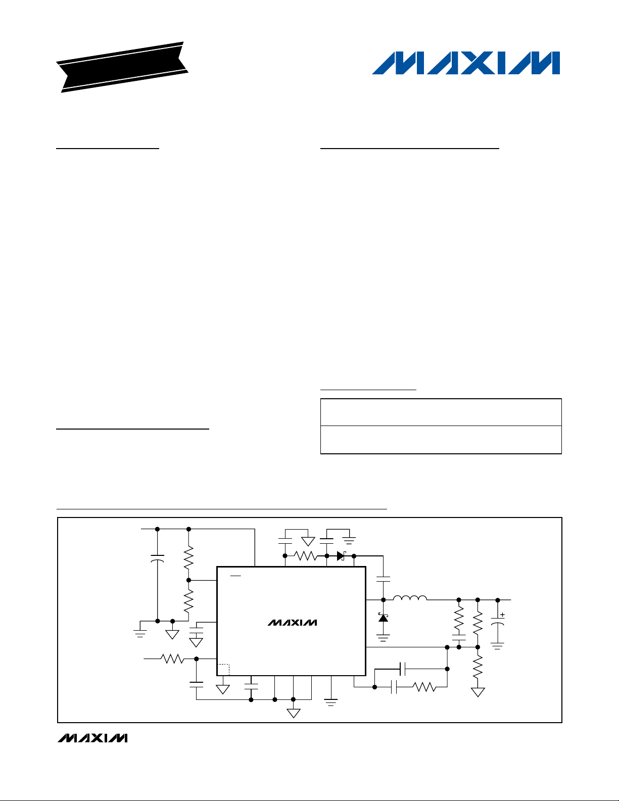
Typical Operating Circuit
19-0811; Rev 0; 4/07
For pricing, delivery, and ordering information, please contact Maxim/Dallas Direct! at
1-888-629-4642, or visit Maxim’s website at www.maxim-ic.com.
+
Denotes a lead-free package.
*
EP = Exposed pad.
PART
TEMP RANGE
PINPACKAGE
PKG
CODE
MAX15020ATP+
T2055-5
Pin Configuration appears at end of data sheet.
EVALUATION KIT
AVAILABLE
-40°C to +125°C
20 TQFN-EP*
(5mm x 5mm)
Page 2
MAX15020
2A, 40V Step-Down DC-DC Converter with
Dynamic Output-Voltage Programming
2 _______________________________________________________________________________________
ABSOLUTE MAXIMUM RATINGS
ELECTRICAL CHARACTERISTICS
(VIN= 36V, V
REG
= V
DVREG
, V
PGND
= V
GND
= VEP= 0V, V
SYNC
= 0V, C
REFOUT
= 0.1µF, TA= TJ= -40°C to +125°C, FSEL = REG,
unless otherwise noted. Typical values are at T
A
= +25°C.) (Note 1)
Stresses beyond those listed under “Absolute Maximum Ratings” may cause permanent damage to the device. These are stress ratings only, and functional
operation of the device at these or any other conditions beyond those indicated in the operational sections of the specifications is not implied. Exposure to
absolute maximum rating conditions for extended periods may affect device reliability.
IN, ON/OFF to GND........…....................................-0.3V to +45V
LX to GND................................................-0.715V to (V
IN
+ 0.3V)
BST to GND ..................................................-0.3V to (V
IN
+ 12V)
BST to LX................................................................-0.3V to +12V
PGND, EP to GND .................................................-0.3V to +0.3V
REG, DVREG, SYNC to GND .................................-0.3V to +12V
FB, COMP, FSEL, REFIN, REFOUT,
SS to GND .............................................-0.3V to (V
REG
+ 0.3V)
Continuous Current through Internal Power MOSFET
T
J
= +125°C..........................................................................4A
T
J
= +150°C.......................................................................2.7A
Continuous Power Dissipation (T
A
= +70°C)
20-Pin Thin QFN, single-layer board (5mm x 5mm)
(derate 21.3mW/°C above +70°C)...........................1702.1mW
20-Pin Thin QFN, multilayer board (5mm x 5mm)
(derate 34.5mW/°C above +70°C)...........................2758.6mW
Maximum Junction Temperature .....................................+150°C
Storage Temperature Range ............................-60°C to +150°C
Lead Temperature (soldering, 10s) ................................+300°C
Input Voltage Range V
UVLO Rising Threshold UVLO
UVLO Falling Threshold UVLO
UVLO Hysteresis UVLO
Quiescent Supply Current VIN = 40V, VFB = 1.3V 1.6 2.8 mA
Switching Supply Current VIN = 40V, VFB = 0V 14.5 mA
Shutdown Current I
ON/OFF CONTROL
Input-Voltage Threshold V
Input-Voltage Threshold
Hysteresis
Input Bias Current V
Shutdown Threshold Voltage V
INTERNAL VOLTAGE REGULATOR (REG)
Output Voltage I
OSCILLATOR
Frequency f
Maximum Duty Cycle D
SYNC/FSEL High-Level Voltage 2 V
SYNC/FSEL Low-Level Voltage 0.8 V
SYNC Frequency Range f
PARAMETER SYMBOL CONDITIONS MIN TYP MAX UNITS
IN
RISING
FALLING
HYST
SHDN
ON/OFF
SD
SW
MAX
SYNC
V
V
V
V
V
V
V
= 0.2V, VIN = 40V 6 15 µA
ON/OFF
rising 1.200 1.225 1.270 V
ON/OFF
= 0V to V
ON/OFF
= 0 to 20mA 7.1 8.3 V
REG
= 0V 450 550
FSEL
= V
FSEL
FSEL
FSEL
FSEL
REG
= 0V 85
= V
REG
= V
REG
IN
7.5 40.0 V
6.80 7.20 7.45 V
6.0 6.5 7.0 V
0.7 V
120 mV
-250 +250 nA
0.2 V
270 330
90
100 550 kHz
kHz
%
Page 3
MAX15020
2A, 40V Step-Down DC-DC Converter with
Dynamic Output-Voltage Programming
_______________________________________________________________________________________ 3
Note 1: Limits are 100% production tested at TA = TJ = +25°C. Limits at -40°C and +125°C are guaranteed by design.
ELECTRICAL CHARACTERISTICS (continued)
(VIN= 36V, V
REG
= V
DVREG
, V
PGND
= V
GND
= VEP= 0V, V
SYNC
= 0V, C
REFOUT
= 0.1µF, TA= TJ= -40°C to +125°C, FSEL = REG,
unless otherwise noted. Typical values are at T
A
= +25°C.) (Note 1)
SOFT-START/REFIN/REFOUT/FB
Soft-Start Current I
REFOUT Output Voltage 0.97 0.98 1.01 V
REFIN Input Range 0 3.6 V
FB Accuracy
FB Input Current VSS = 0.2V, VFB = 0V -250 +250 nA
Open-Loop Gain 80 dB
Unity-Gain Bandwidth 1.8 MHz
PWM Modulator Gain (VIN /
V
)
RAMP
CURRENT-LIMIT COMPARATOR
Cycle-by-Cycle Switch Current
Limit
Number of ILIM Events to Hiccup 4
Hiccup Timeout 512
POWER SWITCH
Switch On-Resistance V
BST Leakage Current V
Switch Leakage Current VIN = 40V, VLX = V
Switch Gate Charge V
THERMAL SHUTDOWN
Thermal Shutdown Temperature T
Thermal Shutdown Hysteresis 20 °C
PARAMETER SYMBOL CONDITIONS MIN TYP MAX UNITS
SS
I
ILIM
SHDN
REFIN = REFOUT 0.97 0.98 1.01 V
FB = COMP, V
f
= 100kHz, VIN = 7.5V 9.4
SYNC
f
= 500kHz, VIN = 40V 8.9
SYNC
- VLX = 6V 0.18 0.35 Ω
BST
= VLX = VIN = 40V 10 µA
BST
- VLX = 6V 10 nC
BST
= 0.2V to 3.6V
REFIN
BST
81526µA
V
REFIN
- 5mV
= 0V 10 µA
V
REFIN
2.5 3.5 4.5 A
+160 °C
V
REFIN
+ 5mV
mV
V/V
—
Clock
periods
Page 4
MAX15020
2A, 40V Step-Down DC-DC Converter with
Dynamic Output-Voltage Programming
4 _______________________________________________________________________________________
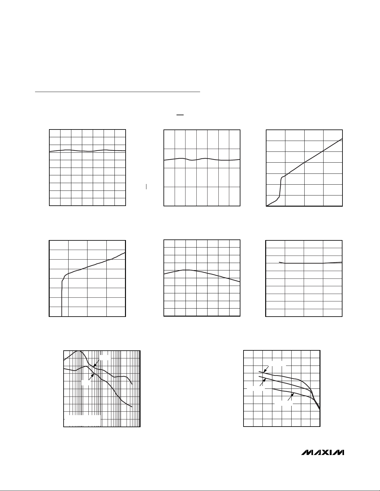
Typical Operating Characteristics
(VIN= 36V, Circuit of Figure 2, TA= +25°C, unless otherwise noted.)
UNDERVOLTAGE LOCKOUT HYSTERESIS
vs. TEMPERATURE
MAX15020 toc01
TEMPERATURE (°C)
UNDERVOLTAGE LOCKOUT HYSTERESIS
1108535 6010-15
0.1
0.2
0.3
0.4
0.5
0.6
0.7
0.8
0.9
1.0
0
-40 135
ON/OFF THRESHOLD HYSTERESIS
vs. TEMPERATURE
MAX15020 toc02
TEMPERATURE (°C)
ON/OFF THRESHOLD HYSTERESIS (V)
1108535 6010-15
0.05
0.10
0.15
0.20
0
-40 135
SHUTDOWN SUPPLY CURRENT
vs. INPUT VOLTAGE
MAX15020 toc03
INPUT VOLTAGE (V)
SUPPLY CURRENT (µA)
302010
1
2
3
4
5
6
7
0
040
NO-LOAD SUPPLY CURRENT
vs. INPUT VOLTAGE
MAX15020 toc04
INPUT VOLTAGE (V)
SUPPLY CURRENT (mA)
302010
2
4
8
6
10
12
14
16
0
040
OPERATING FREQUENCY
vs. TEMPERATURE
MAX15020 toc05
TEMPERATURE (°C)
OPERATING FREQUENCY (kHz)
1108535 6010-15
290
292
294
296
298
300
302
304
306
308
288
-40 135
MAXIMUM DUTY CYCLE
vs. INPUT VOLTAGE
MAX15020 toc06
INPUT VOLTAGE (V)
DUTY CYCLE (%)
302010
86
88
82
84
90
92
94
96
98
100
80
040
LOOP GAIN/PHASE
vs. FREQUENCY
MAX15020 toc07
FREQUENCY (kHz)
GAIN (dB)
PHASE (DEGREES)
100101
-40
-30
-20
-10
0
10
20
30
40
50
-50
-144
-108
-72
-36
0
36
72
108
144
180
-180
0.1 1000
PHASE
VIN = 37V, V
OUT
= 15V,
I
OUT
= 2.02A
GAIN
MAXIMUM LOAD CURRENT
vs. INPUT VOLTAGE
MAX15020 toc08
INPUT VOLTAGE (V)
LOAD CURRENT (A)
353020 2510 155
2.6
2.7
2.8
2.9
3.0
3.1
3.2
3.3
3.4
3.5
2.5
040
TA = -45°C
TA = +25°C
TA = +85°C
Page 5
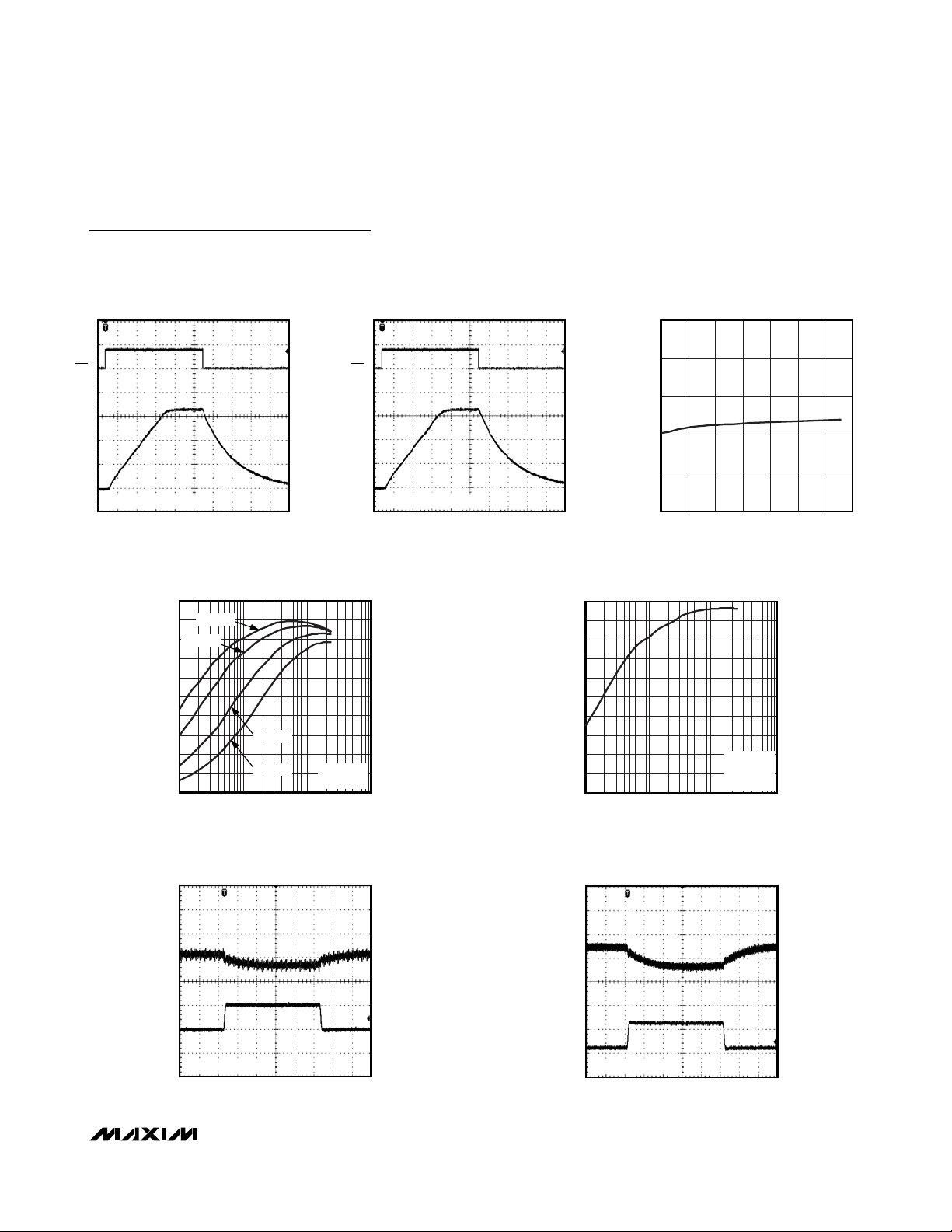
MAX15020
2A, 40V Step-Down DC-DC Converter with
Dynamic Output-Voltage Programming
_______________________________________________________________________________________
5
Typical Operating Characteristics (continued)
(VIN= 36V, Circuit of Figure 2, TA= +25°C, unless otherwise noted.)
LOAD TRANSIENT
MAX15020 toc14
200µs/div
50mV/div
AC-COUPLED
2A
1A
I
OUT
V
OUT
VIN = 12V, V
OUT
= 3.3V
LOAD TRANSIENT
MAX15020 toc15
200µs/div
50mV/div
AC-COUPLED
1.2A
0.2A
V
OUT
I
OUT
VIN = 12V, V
OUT
= 3.3V
TURN-ON/TURN-OFF WAVEFORM
V
OUT
VIN = 40V, R
MAX15020 toc12
V
ON/OFF
TURN-ON/TURN-OFF WAVEFORM
V
OUT
VIN = 12V, R
= 27Ω
LOAD
100
90
80
70
60
50
40
EFFICIENCY (%)
30
20
10
0
MAX15020 toc09
5V/div
V
ON/OFF
0V
1V/div
0V
10ms/div
EFFICIENCY vs. LOAD CURRENT
VIN = 7.5V
VIN = 12V
VIN = 24V
VIN = 40V
0.01 10
OUTPUT CURRENT (A)
fS = 500kHz
V
10.1
OUT
= 3.3V
LOAD
= 27Ω
10ms/div
MAX15020 toc10
REFOUT VOLTAGE vs. TEMPERATURE
1.05
5V/div
0V
1V/div
0V
1.03
1.01
0.99
REFOUT VOLTAGE (V)
0.97
0.95
-40 135
TEMPERATURE (°C)
EFFICIENCY vs. LOAD CURRENT
100
90
80
70
60
50
40
EFFICIENCY (%)
30
20
10
0
0.01 10
OUTPUT CURRENT (A)
10.1
fS = 500kHz
= 40V
V
IN
= 30V
V
OUT
MAX15020 toc11
11085603510-15
MAX15020 toc13
Page 6
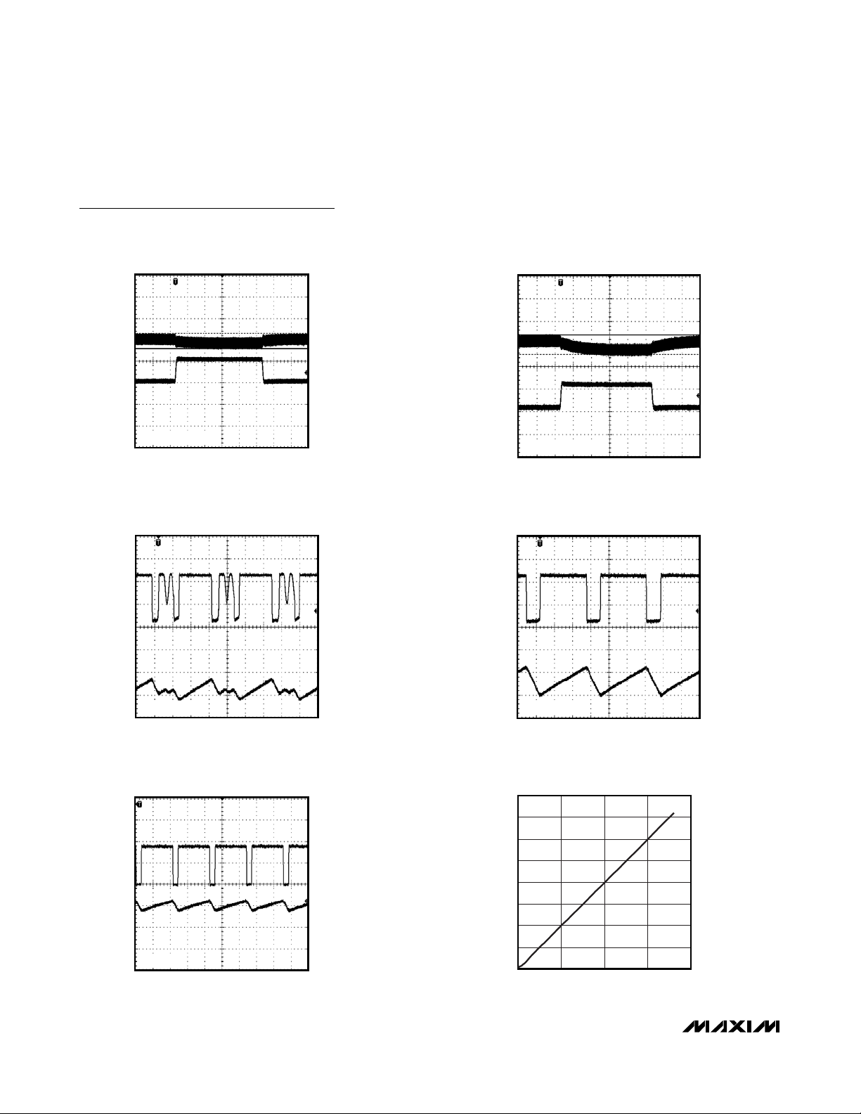
MAX15020
2A, 40V Step-Down DC-DC Converter with
Dynamic Output-Voltage Programming
6 _______________________________________________________________________________________
Typical Operating Characteristics (continued)
(VIN= 36V, Circuit of Figure 2, TA= +25°C, unless otherwise noted.)
HEAVY-LOAD
SWITCHING WAVEFORMS
MAX15020 toc20
1µs/div
20V/div
0V
1A/div
0A
I
LX
V
LX
I
LOAD
= 2A
FEEDBACK VOLTAGE
vs. REFIN INPUT VOLTAGE
MAX15020 toc21
REFIN INPUT VOLTAGE (V)
FEEDBACK VOLTAGE (V)
321
0.5
1.0
1.5
2.0
2.5
3.0
3.5
4.0
0
04
LOAD TRANSIENT
V
OUT
I
OUT
VIN = 40V, V
LIGHT-LOAD SWITCHING WAVEFORMS
V
LX
OUT
= 30V
200µs/div
MAX15020 toc16
MAX15020 toc18
50mV/div
AC-COUPLED
2A
1A
20V/div
0V
LOAD TRANSIENT
V
OUT
I
OUT
VIN = 40V, V
OUT
= 30V
200µs/div
SWITCHING WAVEFORMS
V
LX
MAX15020 toc17
50mV/div
AC-COUPLED
1.1A
0.25A
MAX15020 toc19
20V/div
0V
I
LX
I
= 40mA
LOAD
1µs/div
1A/div
0A
I
LX
I
= 500mA
LOAD
1µs/div
1A/div
0A
Page 7

MAX15020
2A, 40V Step-Down DC-DC Converter with
Dynamic Output-Voltage Programming
_______________________________________________________________________________________
7
Typical Operating Characteristics (continued)
(VIN= 36V, Circuit of Figure 2, TA= +25°C, unless otherwise noted.)
SOFT-START VOLTAGE RISE
vs. REFIN VOLTAGE RISE
MAX15020 toc22
V
REFIN
dv/dt (V/ms)
V
SS
dv/dt (V/ms)
0.1 1
0.1
1
10
0.01
0.01 10
CSS = 0.1µF
CSS = 0.01µF
VSS AND V
OUT
RESPONSE TO REFIN PWM
MAX15020 toc23
2ms/div
1V
0.5V
0V
0V
20V/div
1V/div
1V/div
0V
V
PWM
V
REFIN
V
SS
V
OUT
D = 70% TO 100%
10kΩ and 0.1µF RC ON REFIN
MODULATOR GAIN
vs. INPUT VOLTAGE
MAX15020 toc24
INPUT VOLTAGE (V)
MODULATOR GAIN (V/V)
353025201510
8.5
9.0
9.5
10.0
10.5
11.0
8.0
540
SOFT-START CHARGE CURRENT
vs. TEMPERATURE
MAX15020 toc25
TEMPERATURE (°C)
SOFT-START CHARGE CURRENT (µA)
1108535 6010-15
14.6
14.7
14.8
14.9
15.0
15.1
15.2
15.3
15.4
15.5
14.5
-40 135
Page 8

MAX15020
2A, 40V Step-Down DC-DC Converter with
Dynamic Output-Voltage Programming
8 _______________________________________________________________________________________
Pin Description
PIN NAME FUNCTION
1 COMP Voltage-Error-Amplifier Output. Connect COMP to the necessary compensation feedback network.
2FB
3 ON/OFF
Feedback Regulation Point. Connect to the center tap of an external resistor-divider connected between
the output and GND to set the output voltage. The FB voltage regulates to the voltage applied to REFIN.
ON/OFF Control. The ON/OFF rising threshold is set to approximately 1.225V. Connect to the center tap of
a resistive divider connected between IN and GND to set the turn-on (rising) threshold. Connect ON/OFF to
GND to shut down the IC. Connect ON/OFF to IN for always-on operation given that V
UVLO threshold. ON/OFF can be used for power-supply sequencing.
has risen above the
IN
4 REFOUT
5 SS Soft-Start. Connect a 0.01µF or greater ceramic capacitor from SS to GND. See the Soft-Start (SS) section.
6 REFIN
7 FSEL
8 SYNC
9 DVREG
10 PGND
11 N.C. No Connection. Leave unconnected or connect to GND
12 BST
13, 14, 15 LX Source Connection of Internal High-Side Switch. Connect the inductor and rectifier diode’s cathode to LX.
16, 17, 18 IN Supply Input Connection. Connect to an external voltage source from 7.5V to 40V.
19 REG
20 GND
—EP
0.98V Reference Voltage Output. Bypass REFOUT to GND with a 0.1µF ceramic capacitor. REFOUT is to
be used only with REFIN. It is not to be used to power any other external circuitry.
External Reference Input. Connect to an external reference. V
Connect REFIN to REFOUT to use the internal 1V reference. See the Reference Input and Output (REFIN,
REOUT) section.
Internal Switching Frequency Selection Input. Connect FSEL to REG to select f
to GND to select f
Oscillator Synchronization Input. SYNC can be driven by an external 100kHz to 500kHz clock to
synchronize the MAX15020’s switching frequency. Connect SYNC to GND to disable the synchronization
function. When using SYNC, connect FSEL to REG.
Power Supply for Internal Digital Circuitry. Connect a 10Ω resistor from REG to DVREG. Connect DVREG to
the anode of the boost diode, D2 in Figure 2. Bypass DVREG to GND with at least a 1µF ceramic capacitor.
Power-Ground Connection. Connect the input filter capacitor’s negative terminal, the anode of the
freewheeling diode, and the output filter capacitor’s return to PGND. Connect externally to GND at a single
point near the input bypass capacitor’s return terminal.
High-Side Gate Driver Supply. Connect BST to the cathode of the boost diode and to the positive terminal
of the boost capacitor.
8V Internal Regulator Output. Bypass to GND with at least a 1µF ceramic capacitor. Do not use REG to
power external circuitry.
Ground Connection. Solder the exposed pad to a large GND plane. Connect GND and PGND together at
one point near the input bypass capacitor return terminal.
Exposed Pad. Connect EP to GND. Connecting EP does not remove the requirement for proper ground
connections to the appropriate pins. See the PCB Layout and Routing section.
= 500kHz. When an external clock is connected to SYNC connect FSEL to REG.
SW
regulates to the voltage applied to REFIN.
FB
= 300kHz. Connect FSEL
SW
Page 9

MAX15020
2A, 40V Step-Down DC-DC Converter with
Dynamic Output-Voltage Programming
_______________________________________________________________________________________ 9
Figure 1. Functional Diagram
ON/OFF
REG
REFOUT
REFIN
COMP
SYNC
IN
LDO
REF
EN
REF
THERMAL
SSA
IN
RAMP
REF
ICSS
SS
E/A
FB
EN
OSC
VPOK
SHDN
REF
OK
ENABLE
SWITCHING
REGOK
OVERLOAD
MANAGEMENT
LOGIC
CPWM
ILIM
CLK
MAX15020
IN
HIGH-SIDE
CURRENT
SENSE
REF_ILIM
BST
LX
DVREG
PGND
FSEL
CLK
GND
Page 10

MAX15020
2A, 40V Step-Down DC-DC Converter with
Dynamic Output-Voltage Programming
10 ______________________________________________________________________________________
Figure 2. Typical Application Circuit
Detailed Description
The MAX15020 voltage-mode step-down converter
contains an internal 0.2Ω power MOSFET switch. The
MAX15020 input voltage range is 7.5V to 40V. The
internal low R
DS(ON)
switch allows for up to 2A of output current. The external compensation, voltage feedforward, and automatically adjustable maximum ramp
amplitude simplify the loop compensation design allowing for a variety of L and C filter components. In shutdown, the supply current is typically 6µA. The output
voltage is dynamically adjustable from 0.5V to 36V.
Additional features include an externally programmable
UVLO through the ON/OFF pin, a programmable soft-
start, cycle-by-cycle current limit, hiccup-mode output
short-circuit protection, and thermal shutdown.
Internal Linear Regulator (REG)
REG is the output terminal of the 8V LDO powered from
IN and provides power to the IC. Connect REG externally to DVREG to provide power for the internal digital
circuitry. Place a 1µF ceramic bypass capacitor, C2,
next to the IC from REG to GND. During normal opera-
tion, REG is intended for powering up only the internal
circuitry and should not be used to supply power to the
external loads.
UVLO/ON/
OFF
Threshold
The MAX15020 provides a fixed 7V UVLO function
which monitors the input voltage (V
IN
). The device is
held off until VINrises above the UVLO threshold.
ON/OFF provides additional turn-on/turn-off control.
Program the ON/OFF threshold by connecting a resistive divider from IN to ON/OFF to GND. The device
turns on when V
ON/OFF
rises above the ON/OFF thresh-
old (1.225V), given that VINhas risen above the UVLO
threshold.
Driving ON/OFF to ground places the IC in shutdown.
When in shutdown the internal power MOSFET turns
off, all internal circuitry shuts down, and the quiescent
supply current reduces to 6µA (typ.). Connect an RC
network from ON/OFF to GND to set a turn-on delay
that can be used to sequence the output voltages of
multiple devices.
V
IN
7.5V TO 40V
C3
0.1µF
C1
560µF
PWM
INPUT
R1
97.5kΩ
R2
4.02kΩ
R3
10kΩ
0Ω
C10
1µF
C9
0.1µF
R5
10Ω
C2
1µF
0.22µF
ON/OFF
DVREG
REG
REFIN
C8
IN
SS
REFOUT
C5
0.1µF
D2
MAX15020
SYNC GND FSEL
BST
PGND
COMP
C4
1µF
L1
D1
C13
330pF
22µH
R6
10kΩ
C11
0.027µF
R9
15.8kΩ
LX
FB
EP
C12
0.1µF
R7
10kΩ
0.1µF
R8
340Ω
V
OUT
C7
C6
560µF
Page 11

MAX15020
2A, 40V Step-Down DC-DC Converter with
Dynamic Output-Voltage Programming
______________________________________________________________________________________ 11
Soft-Start (SS)
At startup, after VINis applied and the UVLO threshold
is reached, a 15µA (typ) current is sourced into the
capacitor (C
SS
) connected from SS to GND forcing the
VSSvoltage to ramp up slowly. If V
REFIN
is set to a DC
voltage or has risen faster than the CSScharge rate,
then V
SS
will stop rising once it reaches V
REFIN
. If
V
REFIN
rises at a slower rate, VSSwill follow the V
REFIN
voltage rise rate. V
OUT
rises at the same rate as V
SS
since VFBfollows VSS.
Set the soft-start time (tSS) using following equation:
where t
SS
is in seconds and CSSis in Farads.
Reference Input and
Output (REFIN, REFOUT)
The MAX15020 features a reference input for the internal error amplifier. The IC regulates FB to the SS voltage
which is driven by the DC voltage applied to REFIN.
Connect REFIN to REFOUT to use the internal 0.98V reference. Connect REFIN to a variable DC voltage source
to dynamically control the output voltage. Alternatively,
REFIN can also be driven by a duty-cycle control PWM
source through a lowpass RC filter (Figure 2).
Internal Digital Power Supply (DVREG)
DVREG is the supply input for the internal digital power
supply. The power for DVREG is derived from the output of the internal regulator (REG). Connect a 10Ω
resistor from REG to DVREG. Bypass DVREG to GND
with at least a 1µF ceramic capacitor.
Error Amplifier
The output of the internal error amplifier (COMP) is
available for frequency compensation (see the
Compensation Design
section). The inverting input is
FB, the noninverting input is SS, and the output is
COMP. The error amplifier has an 80dB open-loop gain
and a 1.8MHz GBW product. When an external clock is
used, connect FSEL to REG.
Oscillator/Synchronization Input (SYNC)
With SYNC connected to GND, the IC uses the internal
oscillator and switches at a fixed frequency of 300kHz or
500kHz based upon the selection of FSEL. For external
synchronization, drive SYNC with an external clock from
100kHz to 500kHz and connect FSEL to REG. When driven with an external clock, the device synchronizes to
the rising edge of SYNC.
PWM Comparator/Voltage Feed-Forward
An internal ramp generator is compared against the
output of the error amplifier to generate the PWM signal. The maximum amplitude of the ramp (V
RAMP
) automatically adjusts to compensate for input voltage and
oscillator frequency changes. This causes the V
IN
/
V
RAMP
to be a constant 9V/V across the input voltage
range of 7.5V to 40V and the SYNC frequency range of
100kHz to 500kHz. This simplifies loop compensation
design by allowing large input voltage ranges and
large frequency range selection.
Output Short-Circuit
Protection (Hiccup Mode)
The MAX15020 protects against an output short circuit
by utilizing hiccup-mode protection. In hiccup mode, a
series of sequential cycle-by-cycle current-limit events
cause the part to shut down and restart with a soft-start
sequence. This allows the device to operate with a continuous output short circuit.
During normal operation, the switch current is measured
cycle-by-cycle. When the current limit is exceeded, the
internal power MOSFET turns off until the next on-cycle
and the hiccup counter increments. If the counter
counts four consecutive overcurrent limit events, the
device discharges the soft-start capacitor and shuts
down for 512 clock periods before restarting with a softstart sequence. Each time the power MOSFET turns on
and the device does not exceed the current limit, the
counter is reset.
Thermal-Overload Protection
The MAX15020 features an integrated thermal-overload protection. Thermal-overload protection limits the
total power dissipation in the device and protects it in
the event of an extended thermal fault condition. When
the die temperature exceeds +160°C, an internal thermal sensor shuts down the part, turning off the power
MOSFET and allowing the IC to cool. After the temperature falls by 20°C, the part restarts beginning with the
soft-start sequence.
VC
t
=
SS
×
REFIN SS
A
15µ
Page 12

MAX15020
2A, 40V Step-Down DC-DC Converter with
Dynamic Output-Voltage Programming
12 ______________________________________________________________________________________
Applications Information
Setting the ON/
OFF
Threshold
When the voltage at ON/OFF rises above 1.225V, the
MAX15020 turns on. Connect a resistive divider from IN
to ON/OFF to GND to set the turn-on voltage (see
Figure 2). First select the ON/OFF to the GND resistor
(R2), then calculate the resistor from IN to ON/OFF (R1)
using the following equation:
where V
IN
is the input voltage at which the converter
turns on, V
ON/OFF
= 1.225V and R2 is chosen to be
less than 600kΩ.
If ON/OFF is connected to IN directly, the UVLO feature
monitors the supply voltage at IN and allows operation
to start when VINrises above 7.2V.
Setting the Output Voltage
Connect a resistor-divider from OUT to FB to GND to
set the output voltage (see Figure 2). First calculate the
resistor (R7) from OUT to FB using the guidelines in the
Compensation Design
section. Once R7 is known, cal-
culate R8 using the following equation:
where V
FB
= REFIN and REFIN = 0 to 3.6V.
Setting the Output-Voltage Slew Rate
The output-voltage rising slew rate tracks the VSSslew
rate, given that the control loop is relatively fast compared with the VSSslew rate. The maximum V
SS
upswing slew rate is controlled by the soft-start current
charging the capacitor connected from SS to GND
according to the formula below:
when driving VSSwith a slow-rising voltage source at
REFIN, V
OUT
will slowly rise according to the V
REFIN
slew rate.
The output-voltage falling slew rate is limited to the discharge rate of C
SS
assuming there is enough load current to discharge the output capacitor at this rate. The
C
SS
discharge current is 15µA. If there is no load, then
the output voltage falls at a slower rate based upon
leakage and additional current drain from C
OUT
.
Inductor Selection
Three key inductor parameters must be specified for
operation with the MAX15020: inductance value (L),
peak inductor current (I
PEAK
), and inductor saturation
current (I
SAT
). The minimum required inductance is a
function of operating frequency, input-to-output voltage
differential, and the peak-to-peak inductor current
(∆I
L
). Higher ∆ILallows for a lower inductor value while
a lower ∆I
L
requires a higher inductor value. A lower
inductor value minimizes size and cost and improves
large-signal and transient response, but reduces efficiency due to higher peak currents and higher peak-topeak output voltage ripple for the same output
capacitor. Higher inductance increases efficiency by
reducing the ripple current. Resistive losses due to
extra wire turns can exceed the benefit gained from
lower ripple current levels especially when the inductance is increased without also allowing for larger
inductor dimensions. A good compromise is to choose
∆I
P-P
equal to 40% of the full load current.
Calculate the inductor using the following equation:
VINand V
OUT
are typical values so that efficiency is
optimum for typical conditions. The switching frequency (fSW) is fixed at 300kHz or 500kHz and can vary
between 100kHz and 500kHz when synchronized to an
external clock (see the
Oscillator/Synchronization Input
(SYNC)
section). The peak-to-peak inductor current,
which reflects the peak-to-peak output ripple, is worst
at the maximum input voltage. See the
Output
Capacitor Selection
section to verify that the worst-case
output ripple is acceptable. The inductor saturating
current (I
SAT
) is also important to avoid runaway current during continuous output short circuit. Select an
inductor with an I
SAT
specification higher than the max-
imum peak current limit of 4.5A.
⎣
⎦
RR
12 1=×
⎡
⎢
V
⎢
ON OFF
R
8
R
=
⎡
V
OUT
⎢
V
FB
⎣
V
IN
/
⎤
−
⎥
⎥
7
⎤
1
−
⎥
⎦
VV V
IN OUT OUT
L
=
−()
Vf I
IN SW L
×
××
∆
dV
OUT SS SS
dt
RRRdV
+
78
=
8
RRRI
+
×=
dt
78
8
C
SS
Page 13

MAX15020
2A, 40V Step-Down DC-DC Converter with
Dynamic Output-Voltage Programming
______________________________________________________________________________________ 13
Input Capacitor Selection
The discontinuous input current of the buck converter
causes large input ripple currents and therefore the
input capacitor must be carefully chosen to keep the
input-voltage ripple within design requirements. The
input-voltage ripple is comprised of ∆V
Q
(caused by the
capacitor discharge) and ∆V
ESR
(caused by the ESR
(equivalent series resistance) of the input capacitor).
The total voltage ripple is the sum of ∆V
Q
and ∆V
ESR
.
Calculate the input capacitance and ESR required for a
specified ripple using the following equations:
where:
I
OUT_MAX
is the maximum output current, D is the duty
cycle, and fSWis the switching frequency.
The MAX15020 includes internal and external UVLO
hysteresis and soft-start to avoid possible unintentional
chattering during turn-on. However, use a bulk capacitor if the input source impedance is high. Use enough
input capacitance at lower input voltages to avoid possible undershoot below the UVLO threshold during
transient loading.
Output Capacitor Selection
The allowable output-voltage ripple and the maximum
deviation of the output voltage during load steps determine the output capacitance and its ESR. The output
ripple is mainly composed of ∆VQ(caused by the
capacitor discharge) and ∆V
ESR
(caused by the voltage drop across the ESR of the output capacitor). The
equations for calculating the peak-to-peak output voltage ripple are:
Normally, a good approximation of the output-voltage
ripple is ∆V
RIPPLE
≈ ∆V
ESR
+ ∆VQ. If using ceramic
capacitors, assume the contribution to the output-voltage ripple from ESR and the capacitor discharge to be
equal to 20% and 80%, respectively. ∆I
L
is the peak-to-
peak inductor current (see the
Input Capacitor
Selection
section) and fSWis the converter’s switching
frequency.
The allowable deviation of the output voltage during
fast load transients also determines the output capacitance, its ESR, and its equivalent series inductance
(ESL). The output capacitor supplies the load current
during a load step until the controller responds with a
greater duty cycle. The response time (t
RESPONSE
)
depends on the closed-loop bandwidth of the converter
(see the
Compensation Design
section). The resistive
drop across the output capacitor’s ESR, the drop
across the capacitor’s ESL (∆V
ESL
), and the capacitor
discharge cause a voltage droop during the load step.
Use a combination of low-ESR tantalum/aluminum electrolytic and ceramic capacitors for better transient load
and voltage ripple performance. Surface-mount capacitors and capacitors in parallel help reduce the ESL.
Keep the maximum output-voltage deviations below the
tolerable limits of the electronics powered. Use the following equations to calculate the required ESR, ESL,
and capacitance value during a load step:
where I
STEP
is the load step, t
STEP
is the rise time of the
load step, and t
RESPONSE
is the response time of the
controller.
∆
V
ESR
=
⎛
I
⎜
OUT MAX
⎝
IDD
OUT MAX
C
=
IN
ESR
_
_
∆
Vf
×
QSW
∆
+
2
()
1
×
I
⎞
L
⎟
⎠
−
−()
VV V
∆I
D
IN OUT OUT
=
L
=
Vf L
IN SW
V
OUT
V
IN
×
××
∆
I
∆
V
=
Q
16
=×
∆∆
V ESR I
ESR L
L
××
Cf
OUT SW
V
ESR
=
I
STEP
It
STEP RESPONSE
=
OUT
∆
Vt
ESL STEP
=
×
∆
V
Q
×
I
STEP
ESR
C
ESL
Page 14

MAX15020
2A, 40V Step-Down DC-DC Converter with
Dynamic Output-Voltage Programming
14 ______________________________________________________________________________________
Compensation Design
The MAX15020 uses a voltage-mode control scheme
that regulates the output voltage by comparing the
error-amplifier output (COMP) with an internal ramp to
produce the required duty cycle. The output lowpass
LC filter creates a double pole at the resonant frequency, which has a gain drop of -40dB/decade. The error
amplifier must compensate for this gain drop and
phase shift to achieve a stable closed-loop system.
The basic regulator loop consists of a power modulator,
an output feedback divider, and a voltage error amplifier. The power modulator has a DC gain set by V
IN
/
V
RAMP
, with a double pole and a single zero set by the
output inductance (L), the output capacitance (C
OUT
)
(C6 in the Figure 2) and its ESR. The power modulator
incorporates a voltage feed-forward feature, which automatically adjusts for variations in the input voltage
resulting in a DC gain of 9. The following equations
define the power modulator:
The switching frequency is internally set at 300kHz or
500kHz, or can vary from 100kHz to 500kHz when driven
with an external SYNC signal. The crossover frequency
(fC), which is the frequency when the closed-loop gain is
equal to unity, should be set as f
SW
/ 2π or lower.
The error amplifier must provide a gain and phase
bump to compensate for the rapid gain and phase loss
from the LC double pole. This is accomplished by utilizing a Type 3 compensator that introduces two zeros
and three poles into the control loop. The error amplifier
has a low-frequency pole (fP1) near the origin.
In reference to Figures 3 and 4, the two zeros are at:
And the higher frequency poles are at:
Compensation when fC< f
ESR
Figure 3 shows the error-amplifier feedback as well as
its gain response for circuits that use low-ESR output
capacitors (ceramic). In this case f
ZESR
occurs after fC.
f
Z1
is set to 0.8 x f
LC(MOD)
and fZ2is set to fLCto compensate for the gain and phase loss due to the double
pole. Choose the inductor (L) and output capacitor
(C
OUT
) as described in the
Inductor Selection
and
Output Capacitor Selection
sections.
Choose a value for the feedback resistor R6 in Figure 3
(values between 1kΩ and 10kΩ are adequate).
C12 is then calculated as:
fCoccurs between fZ2and fP2. The error-amplifier gain
(GEA) at fCis due primarily to C11 and R9.
Therefore, GEA(fC) = 2π x fCx C11 x R9 and the modulator gain at fCis:
Since G
EA(fC)
x G
MOD(fC)
= 1, C11 is calculated by:
fP2is set at 1/2 the switching frequency (fSW). R6 is
then calculated by:
Since R7 >> R6, R7 + R6 can be approximated as R7.
R7 is then calculated as:
fP3is set at 5 x fC. Therefore, C13 is calculated as:
V
IN
G
MOD DC
=
f
LC
f
ESR
==
()
V
RAMP
1
×
2
LC
=
2ππ
1
××
C ESR
OUT
f
=
ZZ12
=
f
PP23
2611
1
RC
2912
××
1
××
π
RC
and f
and f
=
9
=
26711
1
RR C
×+×ππ
()
1
12 13
CC
29
π
⎛
××
R
⎜
⎝
12 13
CC
C
12
=
208 9
×××π .
1
fR
LC
G
MOD DC
()
LC f
OUT C
2
MOD DC
()
2
G
MOD fC
()
C
11
2
()=×× ×2
π
fLC
×× ××π
C OUT
=
RG
9
R
6
=
21105
1
Cf
×××π .
SW
R
7
=
1
fC
211
××π
LC
C
C
13
=
2129 1
×
⎞
⎟
⎠
+
12
×××
CRf
P
3
−π
Page 15

MAX15020
2A, 40V Step-Down DC-DC Converter with
Dynamic Output-Voltage Programming
______________________________________________________________________________________ 15
Compensation when fC> f
ZESR
For larger ESR capacitors such as tantalum and aluminum electrolytics, f
ZESR
can occur before fC. If f
ZESR
< fC, then fCoccurs between fP2and fP3. fZ1and f
Z2
remain the same as before, however, fP2is now set
equal to f
ZESR
. The output capacitor’s ESR zero frequency is higher than fLCbut lower than the closedloop crossover frequency. The equations that define
the error amplifier’s poles and zeros (fZ1, fZ2, fP1, fP2,
and fP3) are the same as before. However, fP2is now
lower than the closed-loop crossover frequency. Figure
4 shows the error-amplifier feedback as well as its gain
response for circuits that use higher-ESR output capacitors (tantalum or aluminum electrolytic).
Pick a value for the feedback resistor R9 in Figure 4
(values between 1kΩ and 10kΩ are adequate).
C12 is then calculated as:
The error-amplifier gain between fP2and fP3is approximately equal to R9 / R6 (given that R6 << R7). R6 can
then be calculated as:
C11 is then calculated as:
Since R7 >> R6, R7 + R6 can be approximated as R7.
R7 is then calculated as:
f
P3
is set at 5 x fC. Therefore, C13 is calculated as:
Based on the calculations above, the following compensation values are recommended when the switching frequency of DC-DC converter ranges from 100kHz
to 500kHz. (Note: The compensation parameters in
Figure 2 are strongly recommended if the switching
frequency is from 300kHz to 500kHz.)
Figure 3. Error-Amplifier Compensation Circuit (Closed-Loop
and Error-Amplifier Gain Plot) for Ceramic Capacitors
Figure 4. Error-Amplifier Compensation Circuit (Closed-Loop
and Error-Amplifier Gain Plot) for Higher ESR Output Capacitors
C13
R9
C12
FB
ERROR
AMPLIFIER
SS
f
f
P3
P2
COMP
ERRORAMPLIFIER
GAIN
FREQUENCY (Hz)
GAIN
(dB)
C11
R6
V
OUT
R7
R8
CLOSED-LOOP
GAIN
f
Z1
f
Z2fC
C13
R9
C12
FB
ERROR
AMPLIFIER
SS
f
C
f
P2
f
P3
COMP
ERRORAMPLIFIER
GAIN
FREQUENCY (Hz)
GAIN
(dB)
C11
R6
V
OUT
R7
R8
CLOSED-LOOP
GAIN
f
f
Z1
Z2
C
12
=
208 9
×××π .
1
fR
LC
2
LC
2
f
C
×
R
R
6
=
C
116=
Rf
910
××
C ESR
OUT
R
7
=
C
13
=
2129 1
1
fC
211
××π
LC
C
12
×××
CRf
−π
P
3
Page 16

MAX15020
2A, 40V Step-Down DC-DC Converter with
Dynamic Output-Voltage Programming
16 ______________________________________________________________________________________
Power Dissipation
The MAX15020 is available in a thermally enhanced
package and can dissipate up to 2.7W at T
A
= +70°C.
When the die temperature reaches +160°C, the part
shuts down and is allowed to cool. After the parts cool
by 20°C, the device restarts with a soft-start.
The power dissipated in the device is the sum of the
power dissipated from supply current (PQ), transition
losses due to switching the internal power MOSFET
(P
SW
), and the power dissipated due to the RMS cur-
rent through the internal power MOSFET (P
MOSFET
).
The total power dissipated in the package must be limited such that the junction temperature does not
exceed its absolute maximum rating of +150°C at maximum ambient temperature. Calculate the power lost in
the MAX15020 using the following equations:
The power loss through the switch:
RONis the on-resistance of the internal power MOSFET
(see the
Electrical Characteristics
table).
The power loss due to switching the internal MOSFET:
where tRand tFare the rise and fall times of the internal
power MOSFET measured at LX.
The power loss due to the switching supply current
(I
SW
):
PQ= VINx I
SW
The total power dissipated in the device is:
P
TOTAL
= P
MOSFET
+ PSW+ P
Q
PCB Layout and Routing
Use the following guidelines to layout the switching
voltage regulator:
1) Place the IN and DVREG bypass capacitors close
to the MAX15020 PGND pin. Place the REG
bypass capacitor close to the GND pin.
2) Minimize the area and length of the high-current
loops from the input capacitor, switching MOSFET,
inductor, and output capacitor back to the input
capacitor negative terminal.
3) Keep short the current loop formed by the switching MOSFET, Schottky diode, and input capacitor.
4) Keep GND and PGND isolated and connect them
at one single point close to the negative terminal
of the input filter capacitor.
5) Place the bank of output capacitors close to the
load.
6) Distribute the power components evenly across
the board for proper heat dissipation.
7) Provide enough copper area at and around the
MAX15020 and the inductor to aid in thermal dissipation.
8) Use 2oz copper to keep the trace inductance and
resistance to a minimum. Thin copper PCBs can
compromise efficiency since high currents are
involved in the application. Also, thicker copper
conducts heat more effectively, thereby reducing
thermal impedance.
9) Place enough vias in the pad for the EP of the
MAX15020 so that the heat generated inside can
be effectively dissipated by PCB copper.
PI R
MOSFET RMS MOSFET ON
IIIII
RMS MOSFET
_
P
SW
=×
_
2
=+×
[]
II
PK OUT
II
PK OUT
VI tt f
IN OUT R F SW
=
()
PK
+
=+
+
=
−
××××()
2
PK PK PK
+
∆
I
L
2
∆
I
L
−
2
4
+
−−
D
×
3
Page 17

MAX15020
2A, 40V Step-Down DC-DC Converter with
Dynamic Output-Voltage Programming
______________________________________________________________________________________ 17
Pin Configuration
Chip Information
PROCESS: BiCMOS
TOP VIEW
REG
GND
LX
LX
LX
15 14 12 11
IN
16
IN
17
18
19
20
MAX15020
+
12IN45
FB
COMP
THIN QFN
(5mm x 5mm)
13
3
ON/OFF
BST
REFOUT
N.C.
SS
PGND
10
DVREG
9
8
SYNC
FSEL
7
REFIN
6
Page 18

MAX15020
2A, 40V Step-Down DC-DC Converter with
Dynamic Output-Voltage Programming
18 ______________________________________________________________________________________
Package Information
(The package drawing(s) in this data sheet may not reflect the most current specifications. For the latest package outline information
go to www.maxim-ic.com/packages
.)
PACKAGE OUTLINE,
16, 20, 28, 32, 40L THIN QFN, 5x5x0.8mm
21-0140
QFN THIN.EPS
1
K
2
Page 19

MAX15020
2A, 40V Step-Down DC-DC Converter with
Dynamic Output-Voltage Programming
Maxim cannot assume responsibility for use of any circuitry other than circuitry entirely embodied in a Maxim product. No circuit patent licenses are
implied. Maxim reserves the right to change the circuitry and specifications without notice at any time.
Maxim Integrated Products, 120 San Gabriel Drive, Sunnyvale, CA 94086 408-737-7600 ____________________
19
© 2007 Maxim Integrated Products is a registered trademark of Maxim Integrated Products, Inc.
Package Information (continued)
(The package drawing(s) in this data sheet may not reflect the most current specifications. For the latest package outline information
go to www.maxim-ic.com/packages
.)
PACKAGE OUTLINE,
16, 20, 28, 32, 40L THIN QFN, 5x5x0.8mm
21-0140
2
K
2
 Loading...