

Page 1
General Description
The MAX15009 includes a 300mA LDO regulator, a
switched output, and an overvoltage protection (OVP)
controller to protect downstream circuits from high-voltage load dump. The MAX15011 includes only the 300mA
LDO regulator and switched output. Both devices operate
over a wide supply voltage range from 5V to 40V and are
able to withstand load-dump transients up to 45V. The
MAX15009/MAX15011 feature short-circuit and thermalshutdown protection. These devices offer highly integrated power management solutions for automotive
applications such as instrument clusters, climate control,
and a variety of automotive power-supply circuits.
The 300mA LDO regulator consumes 67µA quiescent
current at light loads and is well suited to power
always-on circuits during “key off” conditions. The LDO
features independent enable and hold inputs, as well
as a microprocessor (µP) reset output with adjustable
reset timeout period.
The switched output of the MAX15009/MAX15011
incorporates a low R
DS(ON)
(0.28Ω, typ) pass transistor
switch internally connected to the output of the LDO
regulator. This switch features accurate current-limit
sensing circuitry and is capable of controlling remote
loads. The MAX15009/MAX15011 feature an adjustable
current limit and a programmable delay timer to set the
overcurrent detection blanking time of the switch and
autoretry timeout.
The MAX15009 OVP controller operates with an external
enhancement mode n-channel MOSFET. While the monitored voltage remains below the adjustable threshold, the
MOSFET stays on. When the monitored voltage exceeds
the OVP threshold, the OVP controller quickly turns off the
external MOSFET. The OVP controller is configurable as a
load-disconnect switch or a voltage limiter.
The MAX15009/MAX15011 are available in a thermally
enhanced, 32-pin (5mm x 5mm), TQFN package and are
fully specified over the -40°C to +125°C automotive operating temperature range.
Applications
Instrument Clusters
Climate Control
AM/FM Radio Power Supply
Multimedia Power Supply
Telematics Power Supply
Features
o 300mA LDO Regulator, Switched Output, and OVP
Controller (MAX15009)
o 300mA LDO Regulator and Switched Output
(MAX15011)
o 5V to 40V Wide Operating Supply Voltage Range
o 45V Load Dump Protection
o 67µA Quiescent Current LDO Regulator
o OVP Controller Disconnects or Limits Output
Voltage During Battery Overvoltage Conditions
o LDO Regulator with Enable, Hold, and Reset
Features
o Internal 0.28Ω (typ) n-Channel Switch for
Switched Output
o 100mA Switched Output with Adjustable Current-
Limit Blanking/Autoretry Delay
MAX15009/MAX15011
Automotive 300mA LDO Regulators with
Switched Output and Overvoltage Protector
________________________________________________________________
Maxim Integrated Products
1
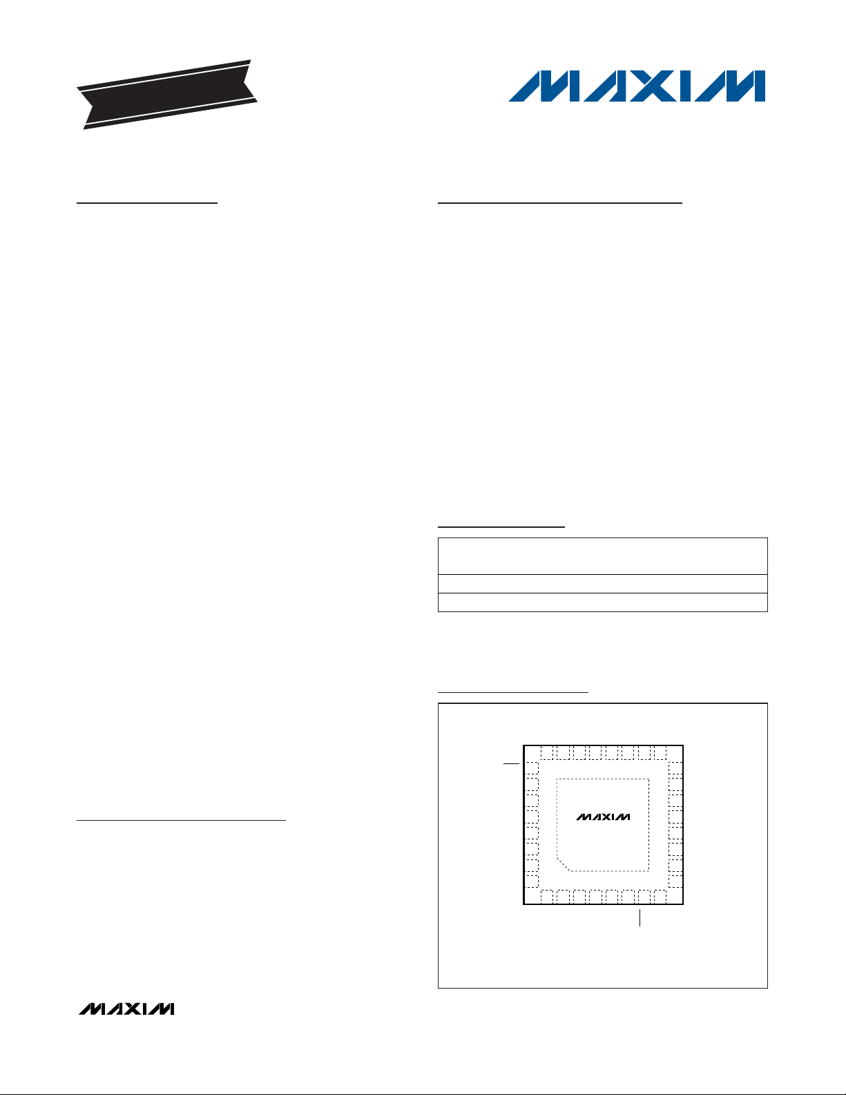
Pin Configurations
19-0923; Rev 1; 2/08
For pricing, delivery, and ordering information, please contact Maxim Direct at 1-888-629-4642,
or visit Maxim’s website at www.maxim-ic.com.
Typical Operating Circuits and Selector Guide appear at end
of data sheet.
Pin Configurations continued at end of data sheet.
Ordering Information
+
Denotes a lead-free package.
For tape and reel, add a T after “+.”
*
EP = Exposed pad.
EVALUATION KIT
AVAILABLE
PART
TEMP RANGE
PINPACKAGE
PKG
CODE
MAX15009ATJ+
T3255-4
MAX15011ATJ+
T3255-4
-40°C to +125°C 32 TQFN-EP*
-40°C to +125°C 32 TQFN-EP*
TOP VIEW
OC_DELAY
OUT_LDO
IN
OUT_LDO
21
MAX15009
4567
3
N.C.
N.C.
SGND
TQFN
(5mm x 5mm)
IN
*EP
PGND
EN_PROT
EN_SW
17
8
N.C.
RESET
16
15
14
13
12
11
10
9
EN_LDO
FB_LDO
N.C.
SOURCE
GATE
N.C.
FB_PROT
CT
HOLD
N.C.
OUT_SW
OUT_SW
N.C.
N.C.
N.C.
N.C.
*EP = EXPOSED PAD
ILIM
2324 22 20 19 18
25
26
27
28
29
30
31
+
32
12
N.C.
N.C.
Page 2

MAX15009/MAX15011
Automotive 300mA LDO Regulators with
Switched Output and Overvoltage Protector
2 _______________________________________________________________________________________
ABSOLUTE MAXIMUM RATINGS
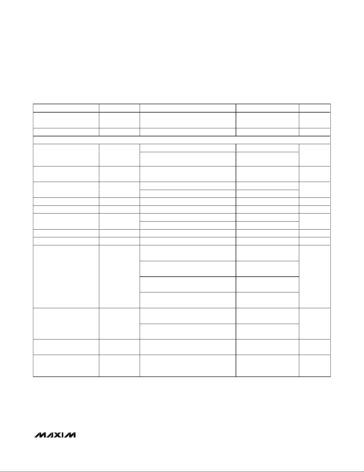
ELECTRICAL CHARACTERISTICS
(VIN= +14V, V
SGND
= V
PGND
= 0V, C
GATE
= 6000pF, CIN= 10µF (ESR < 1.5Ω), C
OUT_LDO
= 22µF (ceramic), C
OUT_SW
= 1µF,
V
OUT_LDO
= 5V, CT= open, TA= TJ= -40°C to +125°C, unless otherwise noted. Typical values are at TA= +25°C.) (Note 1)
Stresses beyond those listed under “Absolute Maximum Ratings” may cause permanent damage to the device. These are stress ratings only, and functional
operation of the device at these or any other conditions beyond those indicated in the operational sections of the specifications is not implied. Exposure to
absolute maximum rating conditions for extended periods may affect device reliability.
(All pins referenced to SGND, unless otherwise noted.)
IN, GATE.................................................................-0.3V to +45V
EN_LDO, EN_SW, EN_PROT ......................-0.3V to (V
IN
+ 0.3V)
SOURCE ......................................................-0.3V to (V
IN
+ 0.3V)
OUT_LDO, FB_LDO, FB_PROT, RESET,
OC_DELAY .........................................................-0.3V to +12V
GATE to SOURCE ..................................................-0.3V to +12V
OUT_SW, ILIM, HOLD ......................-0.3V to (V
OUT_LDO
+ 0.3V)
OUT_SW to OUT_LDO ...........................................-12V to +0.3V
CT to SGND............................................................-0.3V to +12V
SGND to PGND .....................................................-0.3V to +0.3V
IN, OUT_LDO Current .......................................................700mA
OUT_SW Current...............................................................350mA
Current Sink/Source (all remaining pins) ............................50mA
Continuous Power Dissipation (T
A
= +70°C)
32-Pin TQFN (derate 34.5mW/°C above +70°C).............2.7W*
Thermal Resistance
θ
JA
..............................................................................29.0°C/W
θ
JC
................................................................................1.7°C/W
Operating Temperature Range .........................-40°C to +125°C
Junction Temperature......................................................+150°C
Storage Temperature Range .............................-60°C to +150°C
Lead Temperature (soldering, 10s) .................................+300°C
*
As per JEDEC 51 Standard, Multilayer Board (PCB).
Supply Voltage Range V
Supply Current I
Shutdown Supply Current I
IN Undervoltage Lockout V
IN Undervoltage Lockout
Hysteresis
PARAMETER SYMBOL CONDITIONS MIN TYP MAX UNITS
SHDN
V
UVLO_HYST
V
≥ V
IN
IN
UVLO
IN
MAX15009
MAX15011
EN_LDO = EN_SW =
EN_PROT = SGND,
measured from
SGND
VIN falling, GATE disabled 4.10 4.27 4.45 V
+ 1.5V 5 40 V
OUT
EN_LDO = IN, EN_SW =
EN_PROT = 0V, I
= 0µA, LDO on, switch off,
protector off, measured
from SGND
EN_LDO = EN_SW = IN,
EN_PROT = 0V, LDO ON,
I
OUT_LDO
on, I
OUT_SW
protector off, measured
from SGND
EN_LDO = EN_SW =
EN_PROT = IN, LDO ON,
I
OUT_LDO
on, I
OUT_SW
protector on, measured
from SGND
EN_LDO = EN_SW = IN,
LDO ON, I
100µA, switch on, I
= 0µA, measured from
SGND
OUT_LDO
= 100µA, switch
= 0µA,
= 100µA, switch
= 0µA,
OUT_LDO
TA = -40°C to
+85°C
T
A
+125°C
=
OUT_SW
= -40°C to
67 85
290 360
360 500
268 360
16 30
40
260 mV
µA
µA
Page 3
MAX15009/MAX15011
Automotive 300mA LDO Regulators with
Switched Output and Overvoltage Protector
_______________________________________________________________________________________ 3
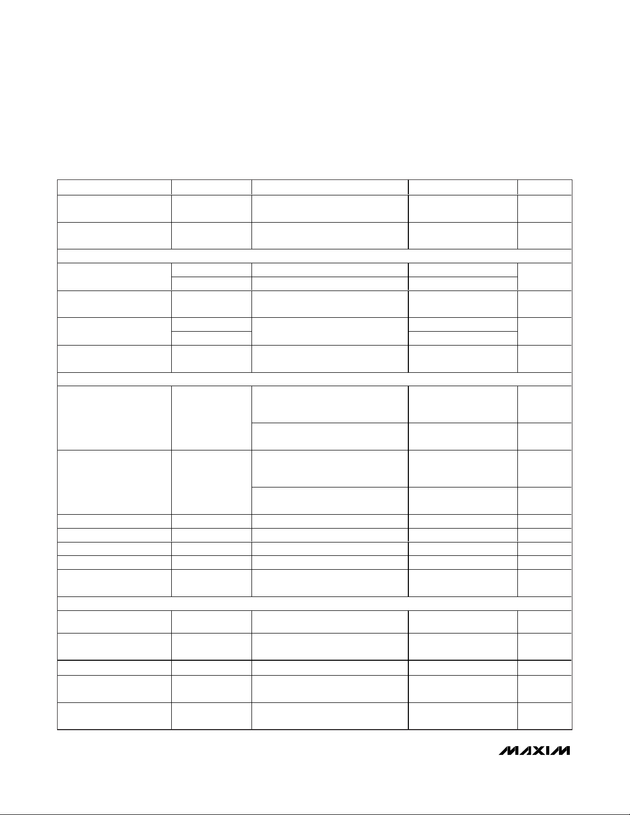
ELECTRICAL CHARACTERISTICS (continued)
(VIN= +14V, V
SGND
= V
PGND
= 0V, C
GATE
= 6000pF, CIN= 10µF (ESR < 1.5Ω), C
OUT_LDO
= 22µF (ceramic), C
OUT_SW
= 1µF,
V
OUT_LDO
= 5V, CT= open, TA= TJ= -40°C to +125°C, unless otherwise noted. Typical values are at TA= +25°C.) (Note 1)
Dual Mode is a trademark of Maxim Integrated Products, Inc.
PARAMETER SYMBOL CONDITIONS MIN TYP MAX UNITS
Thermal-Shutdown
Temperature
Thermal Hysteresis T
LDO
Output Voltage V
FB_LDO Set-Point Voltage V
Dual Mode™ FB_LDO
Threshold
FB_LDO Input Current I
LDO Output Voltage V
LDO Dropout Voltage V
LDO Output Current I
LDO Output Current Limit I
OUT_LDO Line Regulation
OUT_LDO Load Regulation
OUT_LDO Power-Supply
Rejection Ratio
OUT_LDO Startup Delay
Time
t
T
SHDN
HYST
OUT_LDO I
FB_LDO
V
FB_LDO_TH
FB_LDO
LDO_ADJ
DO
OUT_LDO
LIM_LDO
ΔV
/
OUT
ΔV
IN
ΔV
/
OUT
ΔI
OUT
PSRR
STARTUP_DELAY
I
= 1mA, FB_LDO = SGND 4.92 5.00 5.09
LOAD
= 300mA, VIN = 8V,
LOAD
FB_LDO = SGND
With respect to SGND, I
V
OUT_LDO
= 5V, adjustable output option
FB_LDO rising 0.125
FB_LDO falling 0.064
V
= 1V -100 +100 nA
FB_LDO
Adjustable output option (Note 2) 1.8 11.0 V
I
= 300mA (Note 3) 800 1500
LOAD
I
= 200mA (Note 3) 520 1000
LOAD
(Note 4) 300 mA
OUT_LDO = SGND, VIN = 6V 330 500 700 mA
6V ≤ VIN ≤ 40V, I
V
OUT_LDO
6V ≤ VIN ≤ 40V, I
LOAD
= 5V
LOAD
FB_LDO = SGND, V
6V ≤ VIN ≤ 40V, I
LOAD
FB_LDO = SGND, V
6V ≤ VIN ≤ 40V, I
V
OUT_LDO
LOAD
= 3.3V
1mA to 300mA, VIN = 8V,
FB_LDO = SGND
1mA to 300mA, VIN = 6.3V,
V
OUT_LDO
I
LOAD
V
OUT_LDO
I
OUT_LDO
10% of V
= 3.3V
= 10mA, f = 100Hz, 500mV
= 5V
= 0mA, from EN_LDO rising to
OUT_LDO
(nominal),
FB_LDO = SGND
LOAD
= 1mA,
= 1mA,
OUT_LDO
= 20mA,
OUT_LDO
= 20mA,
= 1mA,
= 3.3V
= 5V
P-P
,
+160 °C
20 °C
4.88 5.00 5.11
1.21 1.235 1.26 V
mV
0.03 0.2
0.03 0.1
mV/V
0.27 1
0.27 0.5
0.054 0.15
mV/mA
0.038 0.100
60 dB
30 µs
V
V
Page 4
MAX15009/MAX15011
Automotive 300mA LDO Regulators with
Switched Output and Overvoltage Protector
4 _______________________________________________________________________________________
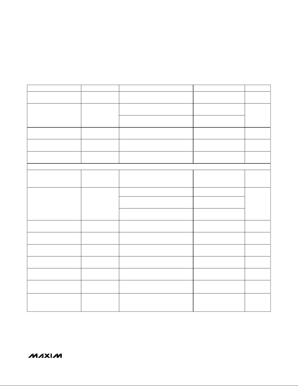
ELECTRICAL CHARACTERISTICS (continued)
(VIN= +14V, V
SGND
= V
PGND
= 0V, C
GATE
= 6000pF, CIN= 10µF (ESR < 1.5Ω), C
OUT_LDO
= 22µF (ceramic), C
OUT_SW
= 1µF,
V
OUT_LDO
= 5V, CT= open, TA= TJ= -40°C to +125°C, unless otherwise noted. Typical values are at TA= +25°C.) (Note 1)
PARAMETER SYMBOL CONDITIONS MIN TYP MAX UNITS
OUT_LDO Overvoltage
Protection Threshold
OUT_LDO Overvoltage
Protection Sink Current
ENABLE/HOLD INPUTS
EN_LDO to EN_PROT Input
Threshold Voltage
E N _LD O, E N _P ROT, E N _S W
Input Pulldown Current
HOLD Input Threshold
Voltage
HOLD Input Pullup I
RESET
RESET Voltage Threshold
HIGH
RESET Voltage Threshold
LOW
V
OUT_LDO
to RESET Delay t
CT Ramp Current I
CT Ramp Threshold V
RESET Output-Voltage Low V
RESET Open-Drain
Leakage Current
LOAD DUMP PROTECTOR (MAX15009 only)
FB_PROT Threshold
Voltage
FB_PROT Threshold
Hysteresis
FB_PROT Input Current I
Startup Response Time t
V
I
EN_PD
HOLD_PU
V
R ESET_H
V
RESET_L
RESET_FALL
I
LEAK_RESET
V
TH_PROT
V
FB_PROT
OV_TH
I
OV
V
IH
V
IL
1mA sink from OUT_LDO 105 110 %V
V
OUT_LDO
= V
OUT
EN_ is internally pulled low to SGND 1 µA
V
IH
V
IL
HOLD is internally pulled high to
OUT_LDO
RESET goes HIGH when rising
V
OUT_LDO
crosses this threshold,
FB_LDO = SGND
RESET goes HIGH when rising
V
crosses this threshold
FB_LDO
RESET goes LOW when falling
V
OUT_LDO
crosses this threshold,
FB_LDO = SGND
RESET goes LOW when falling
CT
CT_TH
OL
V
V
VCT = 0V 1.50 2 2.35 µA
VCT rising 1.190 1.235 1.270 V
I
SINK
crosses this threshold
FB_LDO
OUT_LDO
falling, 0.1V/µs 19 µs
= 1mA, output asserted 0.1 V
Output not asserted 150 nA
FB_PROT rising 1.20 1.235 1.27 V
HYST
START
V
FB_PROT
EN_PROT rising, EN_LDO = IN, to
V
GATE
= 1.4V -100 +100 nA
= 0.5V
(nominal) x 1.15 8 19 mA
2
1.4
0.6 µA
90.0 92.5 95.0 %V
90.0 92.5 95.0 %V
88 90 92 %V
88 90 92 %V
4%V
20 µs
0.7
0.4
OUT_LDO
V
V
OUT_LDO
FB_LDO
OUT_LDO
FB_LDO
TH_PROT
GATE Rise Time t
GATE
GATE rising to +8V, V
= 0V 1 ms
SOURCE
Page 5
MAX15009/MAX15011
Automotive 300mA LDO Regulators with
Switched Output and Overvoltage Protector
_______________________________________________________________________________________ 5
ELECTRICAL CHARACTERISTICS (continued)
(VIN= +14V, V
SGND
= V
PGND
= 0V, C
GATE
= 6000pF, CIN= 10µF (ESR < 1.5Ω), C
OUT_LDO
= 22µF (ceramic), C
OUT_SW
= 1µF,
V
OUT_LDO
= 5V, CT= open, TA= TJ= -40°C to +125°C, unless otherwise noted. Typical values are at TA= +25°C.) (Note 1)
Note 1: Specifications to -40°C are guaranteed by design and not production tested.
Note 2: 1.8V is the minimum limit for proper HOLD functionality.
Note 3: Dropout is defined as V
IN
- V
OUT_LDO
when V
OUT_LDO
is 98% of the value of V
OUT_LDO
for VIN= V
OUT_LDO
+ 1.5V.
Note 4: Maximum output current may be limited by the power dissipation of the package.
PARAMETER SYMBOL CONDITIONS MIN TYP MAX UNITS
FB_PROT to GATE Turn-Off
Propagation Delay
GATE Output High Voltage V
GATE Output Pulldown
Current
GATE Charge-Pump
Current
GATE-to-SOURCE Clamp
Voltage
SWITCH
Switch Dropout ΔV
Switch Current Limit I
Current-Limit Selector ILIM
Voltage
OC_DELAY Timeout
Threshold
OC_DELAY Timeout Pullup
Current
OC_DELAY Timeout
Pulldown Current
Minimum OC_DELAY
Timeout
EN_SW to OUT_SW
Turn-On Time
EN_SW to OUT_SW
Turn-Off Propagation Delay
I
OC_DELAY_DOWN
t
t
OV
- V
GATE
I
V
OC_DELAY
I
OC_DELAY_UP
OC_DELAY_MIN
GATEPD
I
GATE
V
CLMP
SW
SW_LIM
V
ILIM
t
OV_SW
IN
FB_PROT rising from V
250mV to V
V
SOURCE
R
GATE
V
SOURCE
R
GATE
V
GATE
TH_PROT
= VIN = 5.5V,
to IN = 1MΩ
= VIN; VIN ≥ 14V,
to IN = 1MΩ
= 5V, V
EN_PROT
GATE = SGND 45 µA
ΔVSW = V
I
OUT_SW
OUT_LDO
= 100mA, V
no external MOSFET
ILIM = OUT_LDO, VIN = 8V 170 200 240
R
= 100kΩ to SGND,
LIM
V
OUT_LDO
R
LIM
V
OUT_LDO
R
LIM
V
OC_DELAY
V
OC_DELAY
C
OC_DELAY
= 5V, VIN = 8V
= 39kΩ to SGND,
= 5V, VIN = 8V
= 100kΩ
= 0.5V rising
= 0.5V, falling
is unconnected
OUT_SW rising to +0.5V,
OUT_SW
= 1kΩ
R
EN_SW falling, V
rising to +1V, R
V
OUT_LDO
OUT_SW
= 5V
V
+
VIN +
IN
3.2
V
IN
7.0
3.5
+
VIN +
8.1
0.6 µs
VIN +
3.8
VIN +
9.5
TH_PROT
+ 250mV
-
= 0V 63 100 mA
12 16 18 V
- V
OUT_LDO
OUT_SW
,
= 5V,
36 70 mV
85 100 120
30 40 50
0.395 V
1.194 1.235 1.270 V
12.5 16.0 21.3 µA
0.75 1.00 1.40 µA
12 µs
38 µs
OUT_LDO
- V
= 1kΩ,
OUT_SW
18 µs
V
mA
Page 6
MAX15009/MAX15011
Automotive 300mA LDO Regulators with
Switched Output and Overvoltage Protector
6 _______________________________________________________________________________________
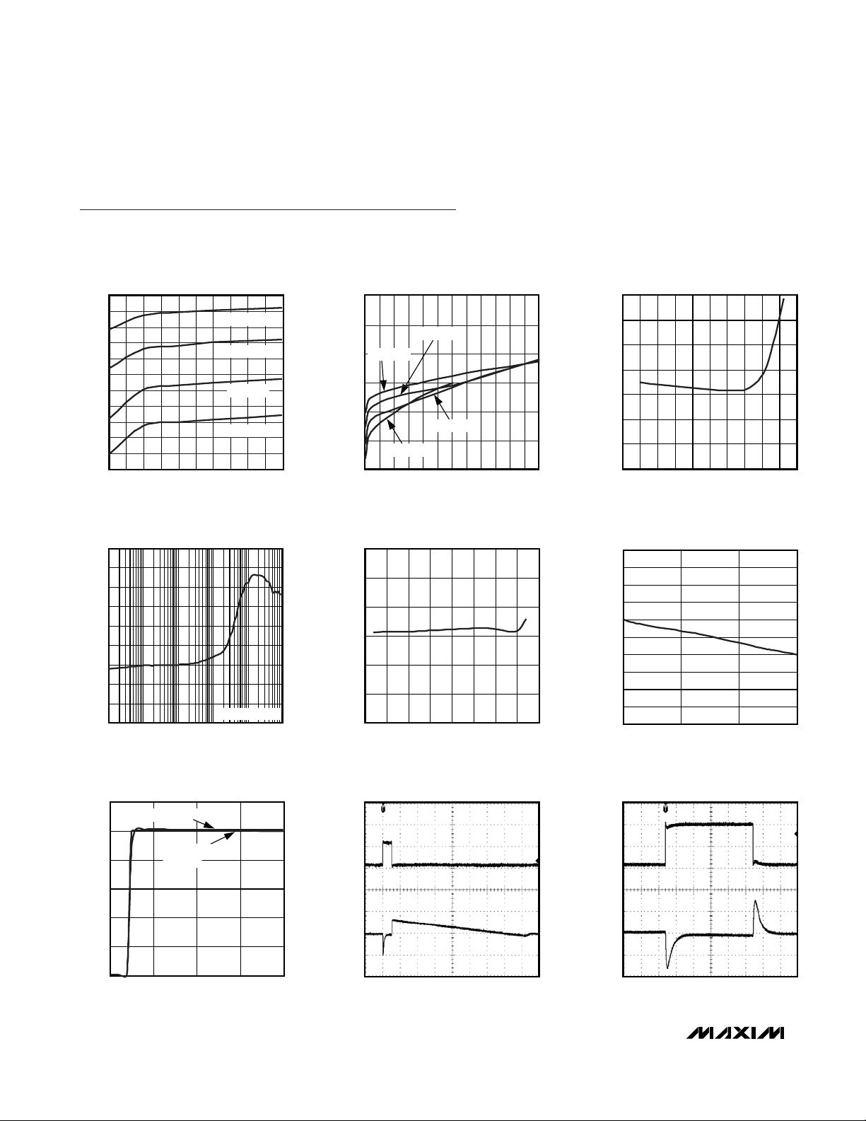
Typical Operating Characteristics
(VIN= V
EN_LDO
= V
EN_PROT
= V
EN_SW
= +14V, CIN= 10µF, C
OUT_LDO
= 22µF, C
OUT_SW
= 1µF, V
OUT_LDO
= +5V, FB_LDO = SGND,
T
A
= +25°C, unless otherwise specified.)
LDO GROUND CURRENT
vs. LOAD CURRENT
MAX15009 toc01
LOAD CURRENT (mA)
0 0.3 0.6 0.90.1 0.4 0.70.2 0.5 0.8 1.0
74
72
70
68
66
64
62
60
58
56
54
52
GROUND CURRENT (μA)
TA = -40°C
TA = +25°C
TA = +125°C
TA = +85°C
LDO GROUND CURRENT
vs. LOAD CURRENT
MAX15009 toc02
LOAD CURRENT (mA)
0 75 150 22525 100 17550 125 200 250 275 300
100
110
90
80
70
60
50
GROUND CURRENT (μA)
TA = -40°C
TA = +25°C
TA = +85°C
TA = +125°C
SHUTDOWN SUPPLY CURRENT
vs. TEMPERATURE
MAX15009 toc03
TEMPERATURE (°C)
-60 0-40 1008060 120-20 20 40 140
30
25
35
20
15
10
5
0
I
SHDN
(μA)
LDO LOAD-TRANSIENT RESPONSE
MAX15009 toc09
400μs/div
I
OUT_LDO
100mA/div
0A
V
OUT_LDO
5V, AC-COUPLED
100mV/div
LDO POWER-SUPPLY
REJECTION RATIO vs. FREQUENCY
MAX15009 toc04
FREQUENCY (Hz)
10 100k10k100 1k 1M
-10
-20
0
-30
-40
-50
-60
-70
-80
-90
LDO PSRR (dB)
I
OUT_LDO
= 10mA
VIN UVLO HYSTERESIS
vs. TEMPERATURE
MAX15009 toc05
TEMPERATURE (°C)
-50 7525-25 125500 100 150
400
350
300
250
200
150
100
UVLO HYSTERESIS (mV)
LDO LOAD REGULATION
MAX15009 toc06
I
OUT_LDO
(mA)
0 200100 300
5.10
5.08
5.06
5.04
5.02
5.00
4.98
4.96
4.94
4.92
4.90
V
OUT_LDO
(V)
LDO LOAD-TRANSIENT RESPONSE
MAX15009 toc08
2ms/div
V
OUT_LDO
5V, AC-COUPLED
20mV/div
I
OUT_LDO
100mA/div
0A
LDO OUTPUT VOLTAGE
vs. INPUT VOLTAGE
MAX15009 toc07
VIN (V)
025155352010 30 40
6
5
4
3
2
1
0
V
OUT_LDO
(V)
I
OUT_LDO
= 10mA
I
OUT_LDO
= 300mA
(PULSED)
Page 7
MAX15009/MAX15011
Automotive 300mA LDO Regulators with
Switched Output and Overvoltage Protector
_______________________________________________________________________________________
7
Typical Operating Characteristics (continued)
(VIN= V
EN_LDO
= V
EN_PROT
= V
EN_SW
= +14V, CIN= 10µF, C
OUT_LDO
= 22µF, C
OUT_SW
= 1µF, V
OUT_LDO
= +5V, FB_LDO = SGND,
T
A
= +25°C, unless otherwise specified.)
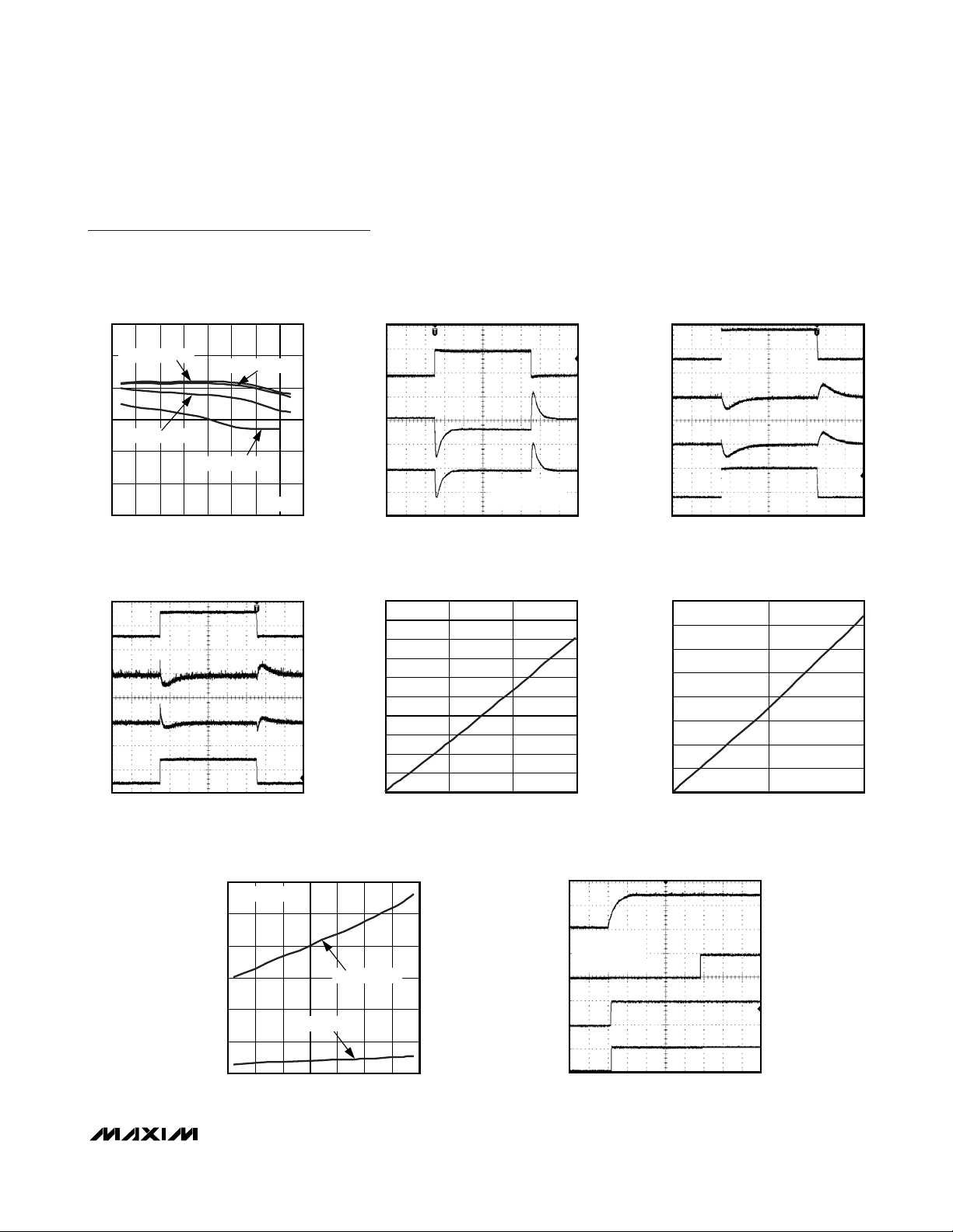
STARTUP RESPONSE THROUGH V
IN
MAX15009 toc17
20ms/div
V
IN
20V/div
0V
0V
0V
0V
V
RESET
5V/div
V
OUT_LDO
5V/div
V
OUT_SW
5V/div
I
OUT_LDO
= 100mA
I
OUT_SW
= 70mA
EN_LDO = EN_SW = IN
5.10
5.05
5.00
(V)
4.95
OUT_LDO
V
4.90
4.85
4.80
10V/div
V
OUT_LDO
3.3V, AC-COUPLED
20mV/div
V
3.3V, AC-COUPLED
OUT_SW
20mV/div
V
OUT_PROT
10V/div
LDO OUTPUT VOLTAGE
vs. TEMPERATURE
I
= 100μA
OUT_LDO
I
= 100mA
OUT_LDO
-50 7525-25 125500 100 150
TEMPERATURE (°C)
LINE-TRANSIENT RESPONSE
V
IN
I
OUT_LDO
40ms/div
I
OUT_LDO
= 300mA
= 10mA
VIN = 8V
MAX15009 toc13
SWITCH LOAD-TRANSIENT RESPONSE
MAX15009 toc10
I
OUT_SW
100mA/div
V
OUT_SW
5V, AC-COUPLED
100mV/div
V
OUT_LDO
5V, AC-COUPLED
100mV/div
LDO DROPOUT VOLTAGE
1000
900
0V
0V
800
700
600
500
400
300
LDO DROPOUT VOLTAGE (mV)
200
100
0
0 200100 300
400μs/div
I
OUT_LDO
I
OUT_SW
vs. LOAD CURRENT
I
(mA)
OUT_LDO
MAX15009 toc11
= 100mA
= 100mA
0A
MAX15009 toc14
20V/div
V
OUT_LDO
3.3V, AC-COUPLED
50mV/div
V
3.3V, AC-COUPLED
OUT_SW
50mV/div
V
OUT_PROT
20V/div
SWITCH DROPOUT VOLTAGE (mV)
LINE-TRANSIENT RESPONSE
V
IN
SWITCH DROPOUT VOLTAGE
vs. LOAD CURRENT
40
35
30
25
20
15
10
5
0
0 10050
40ms/div
I
OUT_SW
(mA)
I
OUT_LDO
MAX15009 toc12
0V
0V
MAX15009 toc15
= 10mA
SWITCH DROPOUT VOLTAGE
vs. TEMPERATURE
60
I
= 10mA
OUT_LDO
50
40
I
= 100mA
30
20
SWITCH DROPOUT VOLTAGE (mV)
10
0
-45 105 13053055-20 80
TEMPERATURE (°C)
I
OUT_SW
OUT_SW
= 10mA
MAX15009 toc16
Page 8
MAX15009/MAX15011
Automotive 300mA LDO Regulators with
Switched Output and Overvoltage Protector
8 _______________________________________________________________________________________
Typical Operating Characteristics (continued)
(VIN= V
EN_LDO
= V
EN_PROT
= V
EN_SW
= +14V, CIN= 10µF, C
OUT_LDO
= 22µF, C
OUT_SW
= 1µF, V
OUT_LDO
= +5V, FB_LDO = SGND,
T
A
= +25°C, unless otherwise specified.)
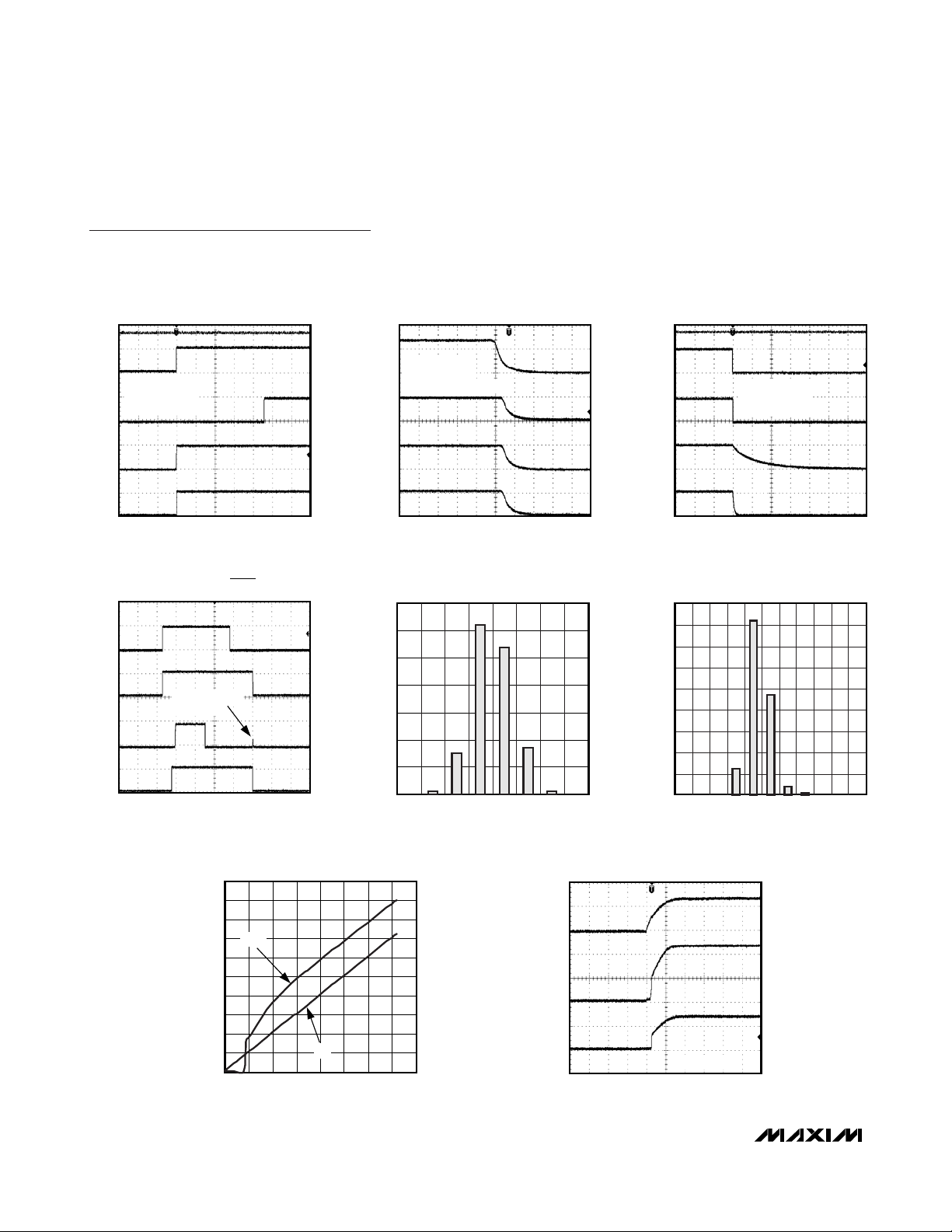
PROTECTOR GATE VOLTAGE
vs. INPUT VOLTAGE (MAX15009 ONLY)
MAX15009 toc24
VIN (V)
20 2515 30 4010 3550
50
40
30
20
45
35
25
10
0
15
5
GATE VOLTAGE (V)
V
GATE
V
IN
GROUND CURRENT DISTRIBUTION
HISTOGRAM (T
A
= +125°C)
MAX15009 toc23
GROUND CURRENT (μA)
67 69 7165
6361
57
59
55
5351
90
40
30
20
10
80
70
60
50
0
NUMBER OF PARTS
STARTUP RESPONSE THROUGH EN
V
IN
V
EN_LDO
5V/div
I
= 100mA
OUT_LDO
= 70mA
I
OUT_SW
V
RESET
5V/div
V
OUT_LDO
5V/div
V
OUT_SW
5V/div
V
EN_LDO
5V/div
V
OUT_LDO
5V/div
HOLD
5V/div
RESET
5V/div
= VEN_SW
V
EN_LDO
20ms/div
LDO, EN_LDO, AND HOLD TIMING
HOLD PULLED UP
TO OUT_LDO
200ms/div
MAX15008 toc18
14V
0V
0V
V
0V
0V
MAX15009 toc21
0V
0V
0V
0V
SHUTDOWN RESPONSE THROUGH V
V
IN
I
OUT_LDO
10V/div
I
OUT_SW
EN_LDO = VEN_SW = IN
V
RESET
5V/div
OUT_LDO
5V/div
V
OUT_SW
5V/div
70
60
50
40
30
NUMBER OF PARTS
20
10
0
67
MAX15008 toc19
= 100mA
= 70mA
2ms/div
GROUND CURRENT DISTRIBUTION
HISTOGRAM (T
GROUND CURRENT (μA)
= -40°C)
A
737169
79
IN
817775
0V
0V
0V
0V
MAX15009 toc22
20V/div
V
EN_LDO
5V/div
V
5V/div
V
OUT_LDO
5V/div
V
OUT_SW
5V/div
SHUTDOWN RESPONSE THROUGH EN
V
IN
I
= 100mA
OUT_LDO
= 70mA
I
RESET
OUT_SW
EN_LDO = EN_SW
MAX15008 toc20
6V
0V
0V
0V
0V
PROTECTOR STARTUP RESPONSE
V
IN
10V/div
V
GATE
10V/div
V
OUT_PROT
10V/div
10ms/div
I
OUT_PROT
MAX15009 toc25
= 1A
0V
0V
0V
Page 9

MAX15009/MAX15011
Automotive 300mA LDO Regulators with
Switched Output and Overvoltage Protector
_______________________________________________________________________________________
9
Typical Operating Characteristics (continued)
(VIN= V
EN_LDO
= V
EN_PROT
= V
EN_SW
= +14V, CIN= 10µF, C
OUT_LDO
= 22µF, C
OUT_SW
= 1µF, V
OUT_LDO
= +5V, FB_LDO = SGND,
T
A
= +25°C, unless otherwise specified.)
RESET TIMEOUT DELAY
vs. TEMPERATURE
MAX15009 toc29
TEMPERATURE (°C)
-25 250 100 12550 15075-50
0
0.6
1.2
1.8
0.4
1.0
1.6
0.2
0.8
1.4
2.0
RESET TIMEOUT DELAY (ms)
C
RESET
= 2.2nF
C
RESET
= 220pF
RESET TIMEOUT DELAY
vs. C
RESET
MAX15009 toc28
C
RESET
(nF)
8621040
7
5
3
6
4
2
0
1
RESET TIMEOUT DELAY (ms)
SWITCH CURRENT LIMIT
vs. ILIM RESISTANCE
MAX15009 toc30
ILIM RESISTANCE (kΩ)
180120 140 1606040 100 2008020
20
60
120
180
40
100
160
80
140
200
SWITCH CURRENT LIMIT (mA)
TA = +125°C
TA = -40°C
TA = +25°C
TA = +85°C
INTERNAL PRESET SWITCH CURRENT LIMIT
vs. TEMPERATURE
MAX15009 toc31
TEMPERATURE (°C)
-25 25 500 125100 15075-50
150
180
210
240
170
160
200
230
190
220
250
PRESET CURRENT LIMIT (mA)
I
OC_DELAY_UP
AND I
OC_DELAY_DOWN
vs. TEMPERATURE
MAX15009 toc32
TEMPERATURE (°C)
-25 25 500 125100 15075-50
0
6
12
4
2
10
16
8
14
18
OC_DELAY PULLUP/PULLDOWN CURRENT (μA)
I
OC_DELAY_DOWN
I
OC_DELAY_UP
OVERVOLTAGE SWITCH FAULT
V
IN
10V/div
20V/div
V
OUT_PROT
20V/div
V
GATE
I
OUT_PROT
= 25V
V
OV
400μs/div
= 1A
MAX15009 toc26
0V
0V
0V
20V/div
V
20V/div
V
OUT_PROT
20V/div
V
IN
GATE
I
OUT_PROT
OV THRESHOLD = 35V
OVERVOLTAGE LIMIT FAULT
= 1A
MAX15009 toc27
40ms/div
0V
0V
0V
Page 10

MAX15009/MAX15011
Automotive 300mA LDO Regulators with
Switched Output and Overvoltage Protector
10 ______________________________________________________________________________________
Pin Description
PIN
1–4, 8, 11,
14, 26, 29–32
1–4, 8,
10–14, 18,
26, 29–32
5 SGND SGND Signal Ground
6 PGND PGND
7 RESET RESET
MAX15009 MAX15011
NAME
N.C. —
— N.C.
FUNCTION
No Connection. Not internally connected.
Ground. PGND is also the return path for the overvoltage protector pulldown current
for the MAX15009. In this case, connect PGND to SGND at the negative terminal of the
bypass capacitor connected to the source of the external MOSFET. For the
MAX15011, connect PGND to SGND together to the local ground plane.
Active-Low Open-Drain Reset Output. RESET is low while OUT_LDO is below the reset
threshold. Once OUT_LDO has exceeded the reset threshold, RESET remains low for
the duration of the reset timeout period then goes high.
9CTCT
10 FB_PROT —
12 GATE —
13 SOURCE —
Reset Timeout Adjust Input. Connect a capacitor (C
the reset timeout period. See the Setting the
Overvoltage-Threshold Adjustment Input. Connect FB_PROT to an external resistive
voltage-divider network to adjust the desired overvoltage threshold. Use FB_PROT to
monitor a system input or output voltage. See the Setting the Overvoltage Threshold
(MAX15009 Only) section.
Protector Gate Drive Output. Connect GATE to the gate of an external n-channel
MOSFET. GATE is the output of a charge pump with a 45µA pullup current to 8.1V
(typ) above IN during normal operation. GATE is quickly turned off through a 63mA
internal pulldown during an overvoltage condition. GATE then remains low until
FB_PROT has decreased below 96% of the overvoltage threshold. GATE pulls low
when EN_PROT is low.
Output-Voltage Sense Input. Connect SOURCE to the source of the external n-channel
MOSFET.
) from CT to ground to adjust
RESET
RESET
Timeout Period section.
Page 11

MAX15009/MAX15011
Automotive 300mA LDO Regulators with
Switched Output and Overvoltage Protector
______________________________________________________________________________________ 11
Pin Description (continued)
PIN
15 FB_LDO FB_LDO
16 EN_LDO EN_LDO
17 EN_SW EN_SW
18 EN_PROT —
19, 20 IN IN Regulator Input. Bypass IN to SGND with a 10µF capacitor with an ESR < 1.5Ω.
21, 22 OUT_LDO OUT_LDO
23 OC_DELAY OC_DELAY
MAX15009 MAX15011
NAME
FUNCTION
LDO Voltage Feedback Input. Connect FB_LDO to SGND to select the preset +5V
output voltage. Connect FB_LDO to an external resistive voltage-divider for adjustable
output operation. See the Setting the Output Voltage section.
Active-High LDO Enable Input. Connect EN_LDO to IN or to a logic-high voltage to
turn on the regulator. To place the LDO in shutdown, pull EN_LDO low or leave
unconnected and leave HOLD unconnected. EN_LDO is internally pulled to SGND
through a 1µA current sink. See the Control Logic section.
Active-High Switch Enable Input. Connect EN_SW to IN or to a logic-high voltage to
turn on the switch. Pull EN_SW low or leave unconnected to place the switch in
shutdown. EN_SW is internally pulled to SGND through a 1µA current sink.
Protector Enable Input. Drive EN_PROT low to force GATE low and turn off the external
n-channel MOSFET. EN_PROT is internally pulled to SGND by a 1µA sink current.
Connect EN_PROT to IN for normal operation.
LDO Regulator Output. Bypass OUT_LDO to SGND with a ceramic capacitor with a
minimum value of 22µF. OUT_LDO has a fixed 5V output or can be adjusted from1.8V
to 11V. See the Setting the Output Voltage section.
Switch Overcurrent Blanking Time Programming Input. Leave OC_DELAY
unconnected to select the minimum delay timeout before turning the switch off.
OC_DELAY is internally pulled to SGND through a 1µA current source. See the
Programming the Switch Overcurrent Blanking Time section.
Switch Current-Limit Set Input. Connect a 10kΩ to 200kΩ resistor from ILIM to SGND to
24 ILIM ILIM
25 HOLD HOLD
27, 28 OUT_SW OUT_SW Switch Output. Bypass OUT_SW to SGND with a minimum 0.1µF ceramic capacitor.
—EPEP
select the current limit for the internal switch. Connect ILIM to OUT_LDO to select the
internal 170mA (min) current-limit threshold. Do not leave ILIM unconnected. See the
Setting the Switch Current Limit section.
Active-Low Hold Input. If EN_LDO is high when HOLD is forced low, the regulator
latches the state of the EN_LDO input and allows the regulator to remain turned on
when EN_LDO is subsequently pulled low. To shut down the regulator, release HOLD
after EN_LDO is pulled low. If HOLD functionality is unused, connect HOLD to
OUT_LDO or leave unconnected. HOLD is internally pulled up to OUT_LDO through a
0.6µA current source. See the Control Logic section.
Exposed Pad. Connect EP to SGND plane. EP also functions as a heatsink to maximize
thermal dissipation. Do not use as the main ground connection.
Page 12

MAX15009/MAX15011
Functional Diagram
Automotive 300mA LDO Regulators with
Switched Output and Overvoltage Protector
12 ______________________________________________________________________________________
ENABLE LDO
HOLD
IN
V
IN
IN
EN_LDO
HOLD
CONTROL
LOGIC
LDO
BIAS AND VOLTAGE
REFERENCE
V
1.235V
REF
5V LDO
OUT_LDO
M
U
X
FB_LDO
OUTPUT
0.925 x V
REF
ENABLE SWITCH
ILIM
EN_SW
OC_DELAY
2μA
V
REF
16μA
V
REF
0.1V
1μA
SWITCH
OUT_SW
VGATE
S
Q
R
0.124V
RESET
OUT_LDO
OUT_SW
CT
RESET
OUTPUT
SWITCH
OUTPUT
IN
GATE UVLO
ENABLE
PROTECTOR
EN_PROT
4.75V
V
REF
OVERVOLTAGE PROTECTOR
EP SGND PGND
(MAX15009 ONLY)
GATE
SOURCE
FB_PROT
V
IN
PROTECTOR
OUTPUT
Page 13

Detailed Description
The MAX15009/MAX15011 integrate a 300mA LDO
voltage regulator, a current-limited switched output,
and an OVP controller (MAX15009 only). These devices
operate over a wide supply voltage range from 5V to
40V and are able to withstand load-dump transients up
to 45V.
The MAX15009/MAX15011 feature a 300mA LDO regulator that consumes 70µA of current under light-load
conditions and feature a fixed 5V or an adjustable output voltage (1.8V to 11V). Connect FB_LDO to ground
to select a fixed 5V output voltage or select the LDO
output voltage by connecting an external resistive voltage-divider at FB_LDO. The regulator sources at least
300mA of current and includes a current limit of 330mA
(min). Enable the LDO by pulling EN_LDO high.
The switch features accurate current-limit sensing circuitry and is capable of controlling remote loads. Once
enabled, an internal charge pump generates the overdrive voltage for an internal MOSFET. The switch then
starts to conduct and OUT_SW is charged up to
V
OUT_LDO
. The switch is enabled when the output volt-
age of the LDO is above the RESET threshold voltage
(92.5% of the LDO nominal output value).
An overcurrent condition exists when the current at
OUT_SW, I
OUT_SW
, exceeds the 200mA (typ) internal
factory-set current-limit threshold or the externally
adjustable current-limit threshold. During a continuous
overcurrent event, the capacitor connected at
OC_DELAY, C
OC_DELAY
, is charged up to a voltage of
1.235V with a current, I
OC_DELAY_UP
. When this voltage
is reached, an overcurrent latch is set and the gate of
the internal MOSFET is discharged, reducing I
OUT_SW
.
C
OC_DELAY
is then discharged through a pulldown cur-
rent, I
OC_DELAY_DOWN(IOC_DELAY_UP
/ 16) and the
internal MOSFET remains off until C
OC_DELAY
has been
discharged to 0.1V. After this user-programmable turnoff delay, the switch turns back on. This charge/
discharge is repeated if the overcurrent condition persists. The switch returns to normal operation once the
overcurrent condition has been removed.
The OVP controller (MAX15009 only) relies on an external MOSFET with adequate voltage rating (V
DSS
) to
protect downstream circuitry from overvoltage transients. The OVP controller drives the gate of the external n-channel MOSFET, and is configurable to operate
as an overvoltage protection switch or as a closed-loop
voltage limiter.
GATE Voltage (MAX15009 Only)
The MAX15009 uses a high-efficiency charge pump to
generate the GATE voltage for the external n-channel
MOSFET. Once the input voltage, V
IN
, exceeds the
undervoltage lockout (UVLO) threshold, the internal
charge pump fully enhances the external n-channel
MOSFET. An overvoltage condition occurs when the
voltage at FB_PROT goes above the threshold voltage,
V
TH_PROT
. After V
TH_PROT
is exceeded, GATE is quickly pulled to PGND with a 63mA pulldown current. The
MAX15009 includes an internal clamp from GATE to
SOURCE that ensures that the voltage at GATE never
exceeds one diode drop below SOURCE during gate
discharge. The voltage clamp also prevents the GATEto-SOURCE voltage from exceeding the absolute maximum rating for the V
GS
of the external MOSFET in case
the source terminal is accidentally shorted to 0V.
Overvoltage Monitoring (MAX15009 Only)
The OVP controller monitors the voltage at FB_PROT
and controls an external n-channel MOSFET, isolating,
or limiting the load during an overvoltage condition.
Operation in OVP switch mode or limiter mode
depends on the connection between FB_PROT and the
external MOSFET.
Overvoltage Switch Mode
When operating in OVP switch mode, the FB_PROT
divider is connected to the drain of the external MOSFET. The feedback path consists of the voltage-divider
tapped at FB_PROT, FB_PROT’s internal comparator,
the internal gate charge pump/gate pulldown, and the
external n-channel MOSFET (Figure 1). When the programmed overvoltage threshold is exceeded, the internal comparator quickly pulls GATE to ground and turns
MAX15009/MAX15011
Automotive 300mA LDO Regulators with
Switched Output and Overvoltage Protector
______________________________________________________________________________________ 13
Figure 1. Overvoltage-Limiter Switch Configuration (MAX15009)
V
IN
IN
FB_PROT
GATE
MAX15009
SOURCE
SGND
PROTECTOR
OUTPUT
Page 14

MAX15009/MAX15011
Automotive 300mA LDO Regulators with
Switched Output and Overvoltage Protector
14 ______________________________________________________________________________________
off the external MOSFET, disconnecting the power
source from the load. In this configuration, the voltage
at the source of the MOSFET is not monitored. When
the voltage at FB_PROT decreases below the overvoltage threshold, the MAX15009 raises the voltage at
GATE, reconnecting the load to the power source.
Overvoltage-Limiter Mode (MAX15009 Only)
When operating in overvoltage-limiter mode, the feedback path consists of SOURCE, FB_PROT’s internal
comparator, the internal gate charge pump/gate pulldown, and the external n-channel MOSFET (Figure 2).
This configuration results in the external MOSFET operating as a hysteretic voltage regulator.
During normal operation, GATE is enhanced 8.1V above
VIN. The external MOSFET source voltage is monitored
through a resistive voltage-divider between SOURCE
and FB_PROT. When V
SOURCE
exceeds the adjustable
overvoltage threshold, an internal pulldown switch
discharges the gate voltage and quickly turns the
MOSFET off. Consequently, the source voltage begins
to fall. The V
SOURCE
fall time is dependent on the MOSFET’s gate charge, the internal charge-pump current,
the output load, and any load capacitance at SOURCE.
When the voltage at FB_PROT is below the overvoltage
threshold by an amount equal to the hysteresis, the
charge pump restarts and turns the MOSFET back on.
In this way, the OVP controller attempts to regulate
V
SOURCE
around the overvoltage threshold. SOURCE
remains high during overvoltage transients and the
MOSFET continues to conduct during an overvoltage
event. The hysteresis of the FB_PROT comparator and
the gate turn-on delay force the external MOSFET to
operate in a switched on/off sequence during an overvoltage event.
Exercise caution when operating the MAX15009 in voltage-limiting mode for long durations. Care must be
taken against prolonged or repeated exposure to overvoltage events while delivering large amounts of load
current as the power dissipation in the external MOSFET may be high under these conditions. To prevent
damage to the MOSFET, implement proper heatsinking.
The capacitor tied between SOURCE and ground may
also be damaged if the ripple current rating for the
capacitor is exceeded.
As the transient voltage decreases, the voltage at
SOURCE falls. For fast-rising transients and very large
MOSFETs, connect an additional capacitor from GATE
to PGND. This capacitor acts as a voltage-divider working against the MOSFET’s drain-to-gate capacitance. If
using a very low gate charge MOSFET, additional
capacitance from GATE to ground might be required to
reduce the switching frequency.
Control Logic
The MAX15009/MAX15011 LDO features two logic
inputs, EN_LDO and HOLD, making these devices suitable for automotive applications. For example, when
the ignition key signal drives EN_LDO high, the regulator turns on and remains on even if EN_LDO goes low,
as long as HOLD is forced low and stays low after initial
regulator power-up. In this state, releasing HOLD turns
the regulator output (OUT_LDO) off. This feature makes
it possible to implement a self-holding circuit without
external components. Forcing EN_LDO low and HOLD
high (or unconnected) places the regulator into shutdown mode, reducing the supply current to less than
16µA. Table 1 shows the state of OUT_LDO with
respect to EN_LDO and HOLD. Leave HOLD uncon-
nected or connect directly to OUT_LDO to allow the
EN_LDO input to act as a standard on/off logic input for
the regulator.
Figure 2. Overvoltage Limiter (MAX15009)
V
IN
IN
GATE
MAX15009
SOURCE
FB_PROT
SGND
PROTECTOR
OUTPUT
Page 15

Applications Information
Load Dump
Most automotive applications run off a multicell 12V
lead-acid battery with a nominal voltage that swings
between 9V and 16V, depending on load current,
charging status, temperature, and battery age, etc. The
battery voltage is distributed throughout the automobile
and is locally regulated down to voltages required by
the different system modules. Load dump occurs when
the alternator is charging the battery and the battery
becomes disconnected. Power in the alternator (behaving now essentially as an inductor) flows into the distributed power system and elevates the voltage seen at
each module. The voltage spikes have rise times typically greater than 5ms and decay within several hundred milliseconds but can extend out to 1s or more
depending on the characteristics of the charging system. These transients are capable of destroying semiconductors on the first fault event.
The MAX15009/MAX15011 feature load-dump transient
protection up to +45V.
Setting the Output Voltage
The MAX15009/MAX15011 feature dual-mode operation: these devices operate in either a preset voltage
mode or an adjustable mode. In preset voltage mode,
internal feedback resistors set the linear regulator output voltage (V
OUT_LDO
) to 5V. To select the preset 5V
output voltage, connect FB_LDO to SGND.
To select an adjustable output voltage between 1.8V
and 11V, use two external resistors connected as a
voltage-divider to FB_LDO (Figure 3). Set the output
voltage using the following equation:
V
OUT_LDO
= V
FB_LDO
x (R1+ R2) / R
2
where V
FB_LDO
= 1.235V and R2≤ 50kΩ.
Setting the
RESET
Timeout Period
The reset timeout period is adjustable to accommodate
a variety of applications. Set the reset timeout period by
connecting a capacitor, C
RESET
, between CT and
SGND. Use the following formula to select the reset
timeout period, t
RESET
:
t
RESET
= C
RESET
x V
CT_TH
/ I
CT
where t
RESET
is in seconds and C
RESET
is in µF.
V
CT_TH
is the CT ramp threshold in volts and ICTis the
CT ramp current in µA, as described in the
Electrical
Characteristics
table.
MAX15009/MAX15011
Automotive 300mA LDO Regulators with
Switched Output and Overvoltage Protector
______________________________________________________________________________________ 15
Figure 3. Setting the LDO Output Voltage
Table 1. EN_LDO/
HHOOLLDD
Truth/State Table
OPERATION STATE EN_LDO HOLD OUT_LDO COMMENT
Initial State Low Don’t care OFF
Turn-On State High Don’t care ON
Hold Setup State High Low ON
Hold State Low Low ON
Off State Low
High or
unconnected
OFF
EN_LDO is pulled to SGND through an internal pulldown. HOLD
is unconnected and is internally pulled up to OUT_LDO. The
regulator is disabled.
EN_LDO is externally driven high turning regulator on. HOLD is
pulled up to OUT_LDO.
HOLD is externally pulled low while EN_LDO remains high
(latches EN_LDO state).
EN_LDO is driven low or left unconnected. HOLD remains
externally pulled low keeping the regulator on.
HOLD is driven high or left unconnected while EN_LDO is low.
The regulator is turned off and EN_LDO/HOLD logic returns to the
initial state.
V
IN
IN
MAX15009
MAX15011
OUT_LDO
FB_LDO
SGND
R1
R2
Page 16

MAX15009/MAX15011
Leave CT open to select a typical reset timeout of 19µs.
To maintain reset accuracy, use a low-leakage type of
capacitor.
Setting the Switch Current Limit
The switch block features accurate current-limit sensing circuitry. A resistor connected from ILIM to SGND
can be used to select the current-limit threshold using
the following relationship:
I
SW_LIM
(mA) = R
ILIM
(kΩ) x 1mA / kΩ
where 20kΩ ≤ R
ILIM
≤ 200kΩ.
Connect ILIM to OUT_LDO to select the default current
limit of 200mA (typ).
Programming the Switch
Overcurrent Blanking Time
The switch provides an adjustable overcurrent blanking
time to allow the safe charge of large capacitive loads.
When an overcurrent event is detected, a delay period
elapses before the condition is latched and the internal
MOSFET is turned off. This period is the overcurrent
delay, t
OC_DELAY
. Set the overcurrent delay using the
following equation:
t
OC_DELAY
= C
OC_DELAY
x V
OC_DELAY
/ I
OC_DELAY_UP
where t
OC_DELAY
is in seconds and C
OC_DELAY
is in
µF. V
OC_DELAY
is the overcurrent delay timeout thresh-
old voltage in volts and I
OC_DELAY_UP
is the overcur-
rent delay timeout pullup current in µA as seen in the
Electrical Characteristics
table.
Ensure that the switch is not disabled due to a large
startup inrush current by selecting a large enough
value for overcurrent blanking time. Assume that the
current available for charging the total switch output
capacitance, C
OUT_SW
, is the difference between the
current-limit threshold value, I
SW_LIM
, and the nominal
DC load current at OUT_SW, I
OUT_SW_NOM
and select
the C
OC_DELAY
using the following relationship:
C
OC_DELAY
also affects the length of time before the
MAX15009/MAX15011 attempt to turn the switch back
on. Set the autoretry delay using the following equation:
t
OC_RETRY
= C
OC_DELAY
x
V
OC_DELAY/IOC_DELAY_DOWN
where t
OC_RETRY
is in seconds, C
OC_DELAY
is in µF,
V
OC_DELAY
is in volts, and I
OC_DELAY_DOWN
is in µA.
C
OC_DELAY
should be a low-leakage type of capacitor
with a minimum value of 100pF.
Setting the Overvoltage Threshold
(MAX15009 Only)
The MAX15009 provides an accurate means to set the
overvoltage threshold for the OVP controller using
FB_PROT. Use a resistive voltage-divider to set the
desired overvoltage threshold (Figure 4). FB_PROT has
a rising 1.235V threshold with a 4% falling hysteresis.
Begin by selecting the total end-to-end resistance,
R
TOTAL
= R3+ R4. Choose R
TOTAL
to yield a total current
equivalent to a minimum of 100 x I
FB_PROT
(FB_PROT’s
input maximum bias current) at the desired overvoltage
threshold. See the
Electrical Characteristics
table.
For example:
With an overvoltage threshold (VOV) set to 20V, R
TOTAL
< 20V / (100 x I
FB_PROT
), where I
FB_PROT
is FB_PROT’s
maximum 100nA bias current:
R
TOTAL
< 2MΩ
Automotive 300mA LDO Regulators with
Switched Output and Overvoltage Protector
16 ______________________________________________________________________________________
Figure 4. Setting the Overvoltage Threshold (MAX15009)
C
OC_DELAY
IVC
OC_DELAY_UP OUT_LDO OUT_SW
≥
V(II )
OC_DELAY SW_LIM OUT_SW_NOM
×−
××
V
IN
R5
R6
IN
FB_PROT
MAX15009
SGND
GATE
PROTECTOR
OUTPUT
SOURCE
V
IN
IN
GATE
MAX15009
SOURCE
FB_PROT
SGND
PROTECTOR
OUTPUT
R3
R4
Page 17

Use the following formula to calculate R4:
R4= V
TH_PROT
x R
TOTAL
/ V
OV
where V
TH_PROT
is the 1.235V FB_PROT rising threshold
and VOVis the desired overvoltage threshold. R4= 124kΩ:
R
TOTAL
= R3+ R
4
where R3= 1.88MΩ. Use a standard 1.87MΩ resistor.
A lower value for total resistance dissipates more
power, but provides better accuracy and robustness
against external disturbances.
Input Transients Clamping
When the external MOSFET is turned off during an
overvoltage event, stray inductance in the power path
may cause additional input-voltage spikes that exceed
the V
DSS
rating of the external MOSFET or the absolute
maximum rating for the MAX15009. Minimize stray
inductance in the power path using wide traces and
minimize the loop area included by the power traces
and the return ground path.
For further protection, add a zener diode or transient
voltage suppressor (TVS) rated below the absolute
maximum rating limits (Figure 5).
External MOSFET Selection
Select the external MOSFET with adequate voltage rating,
V
DSS
, to withstand the maximum expected load-dump
input voltage. The on-resistance of the MOSFET,
R
DS(ON)
, should be low enough to maintain a minimal
voltage drop at full load, limiting the power dissipation
of the MOSFET.
During regular operation, the power dissipated by the
MOSFET is:
P
NORMAL
= I
LOAD
2
x R
DS(ON)
Normally, this power loss is small and is safely handled
by the MOSFET. However, when operating the
MAX15009 in overvoltage limiter mode under prolonged or frequent overvoltage events, select an external MOSFET with an appropriate power rating.
During an overvoltage event, the power dissipation in
the external MOSFET is proportional to both load current and to the drain-source voltage, resulting in high
power dissipated in the MOSFET (Figure 6). The power
dissipated across the MOSFET is:
P
OV_LIMITER
= VQ1x I
LOAD
where VQ1is the voltage across the MOSFET’s drain
and source during overvoltage limiter operation, and
I
LOAD
is the load current.
MAX15009/MAX15011
Automotive 300mA LDO Regulators with
Switched Output and Overvoltage Protector
______________________________________________________________________________________ 17
Figure 5. Protecting the MAX15009 Input from High-Voltage
Transients
Figure 6. Power Dissipated Across MOSFETs During an
Overvoltage Fault (Overvoltage Limiter Mode)
V
IN
IN
TVS
MAX15009
GATE
SOURCE
SGND
LOAD
V
MAX
GATE
SOURCE
FB_PROT
+ VQ1 -
I
LOAD
V
LOAD
V
SOURCE
IN
TVS
MAX15009
SGND
SOURCE
V
OV
Page 18

MAX15009/MAX15011
Overvoltage-Limiter Mode
Switching Frequency
When the MAX15009 is configured in overvoltagelimiter mode, the external n-channel MOSFET is subsequently switched on and off during an overvoltage
event. The output voltage at OUT_PROT resembles a
periodic sawtooth waveform. Calculate the period of
the waveform, t
OVP
, by summing three time intervals
(Figure 7):
t
OVP
= t1+ t2+ t
3
where t1is the V
SOURCE
output discharge time, t2 is the
GATE delay time, and t3is the V
SOURCE
output charge
time.
During an overvoltage event, the power dissipated
inside the MAX15009 is due to the gate pulldown current, I
GATEPD
. This amount of power dissipation is
worse when I
SOURCE
= 0 (C
SOURCE
is discharged only
by the internal current sink).
The worst-case internal power dissipation contribution
in overvoltage limiter mode, P
OVP
, in watts can be
approximated using the following equation:
where V
OV
is the overvoltage threshold voltage in volts
and I
GATEPD
is 100mA (max) GATE pulldown current.
Output Discharge Time (t1)
When the voltage at SOURCE exceeds the adjusted
overvoltage threshold, GATE’s internal pulldown is
enabled until V
SOURCE
drops by 4%. The internal cur-
rent sink, I
GATEPD
, and the external load current,
I
LOAD
, discharge the external capacitance from
SOURCE to ground.
Calculate the discharge time, t
1
, using the following
equation:
where t1is in ms, VOVis the adjusted overvoltage
threshold in volts, I
LOAD
is the external load current in
mA, and I
GATEPD
is the 100mA (max) internal pulldown
current of GATE. C
SOURCE
is the value of the capacitor
connected between the source of the MOSFET and
PGND in µF.
GATE Delay Time (t2)
When SOURCE falls 4% below the overvoltage-threshold
voltage, the internal current sink is disabled and the
internal charge pump begins recharging the external
GATE voltage. Due to the external load, the SOURCE
voltage continues to drop until the gate of the MOSFET is
recharged. The time needed to recharge GATE and reenhance the external MOSFET is approximately:
where t2is in µs, C
iss
is the input capacitance of the
MOSFET in pF, and V
GS(TH)
is the GATE-to-SOURCE
threshold voltage of the MOSFET in volts. VFis the 0.7V
(typ) internal clamp diode forward voltage of the MOSFET in volts, and I
GATE
is the charge-pump current
45µA (typ). Any external capacitance between GATE
and PGND adds up to C
iss
.
During t2, the SOURCE capacitance, C
SOURCE
, loses
charge through the output load. The voltage across
C
SOURCE
, ΔV2, decreases until the MOSFET reaches
its V
GS(TH)
threshold. Approximate ΔV2using the fol-
lowing formula:
SOURCE Output Charge Time (t3)
Once the GATE voltage exceeds the GATE-to-SOURCE
threshold, V
GS(TH)
, of the external MOSFET, the MOSFET turns on and the charge through the internal
charge pump with respect to the drain potential, QG,
determines the slope of the output voltage rise. The
time required for the SOURCE voltage to rise again to
the overvoltage threshold is:
Automotive 300mA LDO Regulators with
Switched Output and Overvoltage Protector
18 ______________________________________________________________________________________
Figure 7. MAX15009 Timing Diagram
GATE
SOURCE
t
2
t
1
t
3
t
OVP
PV I
=×× ×0981.
OVP OV GATEPD
t
t
OVP
tC
=×
1 SOURCE
0.04 V
×
OV
II
+
LOAD GATEPD
tC
=×
2
VV
GS TH F
iss
+
()
I
GATE
It
×
ΔV
LOAD
=
2
C
2
SOURCE
CV
×Δ
rss SOURCE
t
=
3
I
GATE
Page 19

where V
SOURCE
= (VOVx 0.04) + V2 in volts, and C
rss
is the MOSFET’s reverse transfer capacitance in pF.
Any external capacitance between GATE and PGND
adds up to C
rss
.
Power Dissipation/Junction Temperature
During normal operation, the MAX15009/MAX15011
have two main sources of internal power dissipation:
the LDO and the switched output.
The internal power dissipation due to the LDO can be
calculated as:
where VINis the LDO input supply voltage in volts,
V
OUT_LDO
is the output voltage of the LDO in volts,
I
OUT_LDO
is the LDO total load current in mA, and
I
OUT_SW
is the switch load current in mA.
Calculate the power dissipation due to the switch as:
where ΔVSWis the switch dropout voltage in volts for
the given I
OUT_SW
current in mA.
The total power dissipation P
DISS
in mW as:
P
DISS
= P
LDO
+ P
SW
For prolonged exposure to overvoltage events, use the
VINvoltage expected during overvoltage conditions.
Under these circumstances the corresponding internal
power dissipation contribution, P
OVP
, calculated in the
previous section should also be included in the total
power dissipation, P
DISS
.
For a given ambient temperature, T
A
, calculate the
junction temperature, TJ, as follows:
TJ= TA+ P
DISS
x θ
JA
where TJand TAare in °C and θJAis the junction-toambient thermal resistance in °C/W as listed in the
Absolute Maximum Ratings
section.
The junction temperature should never exceed +150°C
during normal operation.
Thermal Protection
When the junction temperature exceeds TJ= +160°C,
the MAX15009/MAX15011 shut down to allow the
device to cool. When the junction temperature drops to
+140°C, the thermal sensor turns all enabled blocks on
again, resulting in a cycled output during continuous
thermal-overload conditions. Thermal protection protects the MAX15009/MAX15011 from excessive power
dissipation. For continuous operation, do not exceed
the absolute maximum junction temperature rating of
+150°C.
MAX15009/MAX15011
Automotive 300mA LDO Regulators with
Switched Output and Overvoltage Protector
______________________________________________________________________________________ 19
P(VV )(I I )
=− × +
IN OUT_LDO OUT_LDO OUT_SWLDO
PVI
=×Δ
SW SW
OUT SW_
Page 20

MAX15009/MAX15011
Automotive 300mA LDO Regulators with
Switched Output and Overvoltage Protector
20 ______________________________________________________________________________________
Typical Operating Circuits
DC-DC
MAX5073
C
SOURCE
SOURCE FB_PROT
5V TO 40V INPUT
C
SWITCH ON/OFF
PROTECTOR ON/OFF
R
ILIM
GATE
OUT_SW
OUT_LDO
FB_LDO
RESET
C
OC_DELAY
PGND
SGND
R
PU
SWITCH OUTPUT
C
OUT_SW
5V
300mA
C
OUT_LDO
V
CC
RESET/EN
I/O
μC
IN
IN
EN_LDOLDO ON/OFF
MAX15009
EN_SW
EN_PROT
HOLDHOLD
ILIM
CT OC_DELAY
C
RESET
V
OUT1
V
OUT2
5V TO 40V INPUT
C
IN
R
ILIM
IN
OUT_SW
EN_LDOLDO ON/OFF
EN_SWSWITCH ON/OFF
HOLDHOLD
ILIM
CT PGND SGND
C
RESET
MAX15011
OC_DELAY
C
OC_DELAY
OUT_LDO
FB_LDO
RESET
C
OUT_SW
R
PU
SWITCH OUTPUT
5V
300mA
C
OUT_LDO
V
CC
RESET/EN
I/O
μC
Page 21

MAX15009/MAX15011
Automotive 300mA LDO Regulators with
Switched Output and Overvoltage Protector
______________________________________________________________________________________ 21
Chip Information
PROCESS: BiCMOS
MAX15011
TQFN
(5mm x 5mm)
+
TOP VIEW
29
30
28
27
12
11
13
N.C.
N.C.
SGND
PGND
RESET
14
N.C.
OC_DELAY
OUT_LDO
IN
ILIM
IN
N.C.
12
OUT_SW
4567
2324 22 20 19 18
N.C.
N.C.
N.C.
N.C.
N.C.
N.C.
N.C.
OUT_LDO
3
21
31
10
N.C.
N.C.
32
9
N.C.
CT
OUT_SW
26
15
FB_LDO
*EP
*EP = EXPOSED PAD
N.C.
25
16
EN_LDO
N.C.
EN_SW
8
17
HOLD
Pin Configurations (continued)
PART LDO
SWITCHED
OUTPUT
OVP
CONTROLLER
MAX15009 √√ √
MAX15011 √√ —
Selector Guide
Page 22

MAX15009/MAX15011
Automotive 300mA LDO Regulators with
Switched Output and Overvoltage Protector
22 ______________________________________________________________________________________
Package Information
(The package drawing(s) in this data sheet may not reflect the most current specifications. For the latest package outline information
go to www.maxim-ic.com/packages
.)
QFN THIN.EPS
Page 23

MAX15009/MAX15011
Automotive 300mA LDO Regulators with
Switched Output and Overvoltage Protector
______________________________________________________________________________________ 23
Package Information (continued)
(The package drawing(s) in this data sheet may not reflect the most current specifications. For the latest package outline information
go to www.maxim-ic.com/packages
.)
Page 24

MAX15009/MAX15011
Automotive 300mA LDO Regulators with
Switched Output and Overvoltage Protector
Maxim cannot assume responsibility for use of any circuitry other than circuitry entirely embodied in a Maxim product. No circuit patent licenses are
implied. Maxim reserves the right to change the circuitry and specifications without notice at any time.
24
____________________Maxim Integrated Products, 120 San Gabriel Drive, Sunnyvale, CA 94086 408-737-7600
© 2008 Maxim Integrated Products is a registered trademark of Maxim Integrated Products, Inc.
Revision History
REVISION
NUMBER
0 8/07 Initial release —
1 1/08
REVISION
DATE
Removed future product asterisks, updated Electrical Characteristics table and
Typical Operating Characteristics section.
DESCRIPTION
PAGES
CHANGED
1, 2, 6, 8
 Loading...