

Page 1
General Description
The MAX15006/MAX15007 ultra-low quiescent-current
linear regulators are ideal for use in automotive and
battery-operated systems. These devices operate from
an input voltage of 4V to 40V, deliver up to 50mA of output current, and consume only 10µA of quiescent current at no load. The internal p-channel pass device
keeps the quiescent current low even at full load. The
MAX15007 consumes only 3µA current when in shutdown.
The MAX15006A/MAX15007A have a fixed 3.3V output
while the MAX15006B/MAX15007B have a fixed 5V output voltage. The MAX15007 includes an enable input to
turn the device on or off. All devices are short-circuit
protected and include thermal shutdown.
The MAX15006/MAX15007 operate over the -40°C to
+125°C automotive temperature range. These devices
are available in space-saving 3mm x 3mm 6-pin TDFN
and 8-pin SO thermally enhanced packages.
Applications
Automotive
Tire-Pressure Monitoring
Industrial
Telecom
Networking
Features
o Wide Operating Input Voltage Range (4V to 40V)
o Guaranteed 50mA Output Current
o Low Quiescent Current
10µA (No Load) and 90µA (Full Load)
o Operates Through Cold-Crank Condition
o Withstands 45V Load Dump
o Low Dropout Voltage of 300mV
(MAX15006B/MAX15007B)
o Stable Operation with Tiny 2.2µF Output
Capacitor
o Enable Input (MAX15007)
o Preset 3.3V and 5.0V Output Voltages
o Thermal and Short-Circuit Protection
o -40°C to +125°C Operating Temperature Range
o Thermally Enhanced 3mm x 3mm 6-Pin TDFN/
8-Pin SO Packages
MAX15006/MAX15007
40V, Ultra-Low Quiescent-Current
Linear Regulators in 6-Pin TDFN/8-Pin SO
________________________________________________________________
Maxim Integrated Products
1
Pin Configurations
19-0663; Rev 0; 10/06
For pricing, delivery, and ordering information, please contact Maxim/Dallas Direct! at
1-888-629-4642, or visit Maxim’s website at www.maxim-ic.com.
Pin Configurations continued at end of data sheet.
Ordering Information
Ordering Information continued at end of data sheet.
Note: All devices are specified over the -40°C to +125°C oper-
ating temperature range.
+
Denotes lead-free package.
*
EP = Exposed pad.
TOP VIEW
OUT GND
OUT
654
MAX15006A
MAX15006B
+
123
IN
TDFN
*EP
N.C.IN
PART
MAX15006AASA+ 8 SO-EP* — S8E-12
MAX15006AATT+ 6 TDFN-EP* APE T633-2
MAX15006BASA+ 8 SO-EP* — S8E-12
MAX15006BATT+ 6 TDFN-EP* APF T633-2
PINPACKAGE
TOP
MARK
PKG
CODE
MAX15006A
MAX15006B
+
IN
N.C.
N.C.
1
2
3
*EP
4
*EXPOSED PAD
SO
87OUT
N.C.N.C.
N.C.
6
GND
5
Page 2
MAX15006/MAX15007
40V, Ultra-Low Quiescent-Current
Linear Regulators in 6-Pin TDFN/8-Pin SO
2 _______________________________________________________________________________________
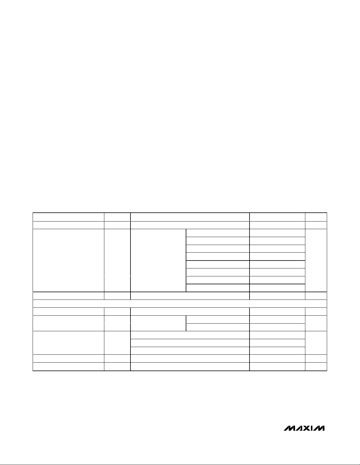
ABSOLUTE MAXIMUM RATINGS
ELECTRICAL CHARACTERISTICS
(VIN= 14V, I
OUT
= 1mA, CIN= 0.1µF, C
OUT
= 2.2µF, TA= TJ= -40°C to +125°C, unless otherwise noted. Typical specifications are
at T
A
= +25°C.) (Note 1)
Stresses beyond those listed under “Absolute Maximum Ratings” may cause permanent damage to the device. These are stress ratings only, and functional
operation of the device at these or any other conditions beyond those indicated in the operational sections of the specifications is not implied. Exposure to
absolute maximum rating conditions for extended periods may affect device reliability.
IN to GND ...............................................................-0.3V to +45V
EN to GND..............................................................-0.3V to +45V
OUT to GND ...........................................................-0.3V to +12V
OUT Short-Circuit Duration ........................................Continuous
Maximum Current Into Any Pin (except IN and OUT) ......±50mA
Continuous Power Dissipation (T
A
= +70°C)
6-Pin TDFN-EP (derate 23.8mW/°C above +70°C) .......1904mW*
8-Pin SO-EP (derate 23.3mW/°C above +70°C) .........1860mW*
Thermal Resistance
θ
JA
, 6-Pin TDFN ...........................................................42°C/W
θ
JC
, 6-Pin TDFN ..........................................................8.5°C/W
θ
JA
, 8-Pin SO-EP ..........................................................43°C/W
θ
JC
, 8-Pin SO-EP............................................................7°C/W
Operating Temperature Range .........................-40°C to +125°C
Junction Temperature......................................................+150°C
Storage Temperature Range .............................-65°C to +150°C
Lead Temperature (soldering, 10s) .................................+300°C
*As per JEDEC51 Standard (Multilayer Board).
Input Voltage Range V
Ground Current I
Shutdown Supply Current I
REGULATOR
Guaranteed Output Current I
Output Voltage V
Line Regulation 6V ≤ VIN ≤ 35V, I
Load Regulation VIN = V
PARAMETER SYMBOL CONDITIONS MIN TYP MAX UNITS
IN
GND
SHDN
OUT
OUTIOUT
Regulator on,
measured at GND
Regulator off (MAX15007 only) 3 5 µA
DO
VIN ≥ V
I
OUT
I
OUT
I
OUT
+ ΔV
OUT
= 1mA (Note 2)
= 5mA, MAX15006B/MAX15007B 30 53
= 50mA, MAX15006B/MAX15007B 300 525Dropout Voltage (Notes 3, 4) ΔV
= 50mA, MAX15006A/MAX15007A 700
+ 3V, I
OUT
440V
I
= 0 (MAX15006) 10 17
OUT
I
= 0 (MAX15007) 11 18
OUT
I
= 100µA (MAX15006) 10.5 18
OUT
I
= 100µA (MAX15007) 11.5 19
OUT
I
= 1mA (MAX15006) 12 20
OUT
I
= 1mA (MAX15007) 13 21
OUT
I
= 50mA (MAX15006) 90 150
OUT
= 50mA (MAX15007) 93 150
I
OUT
DO
MAX15006A/MAX15007A 3.25 3.3 3.35
MAX15006B/MAX15007B 4.925 5.0 5.075
= 1mA 0.25 %
OUT
= 100µA to 50mA 0.7 1.5 %
OUT
50 mA
µA
V
mV
Page 3
MAX15006/MAX15007
40V, Ultra-Low Quiescent-Current
Linear Regulators in 6-Pin TDFN/8-Pin SO
_______________________________________________________________________________________ 3
Note 1: Limits at -40°C are guaranteed by design.
Note 2: Output voltage regulation is guaranteed for I
OUT
≥ 5µA.
Note 3: Dropout voltage is defined as (V
IN
- V
OUT
) when V
OUT
is 2% below the value of V
OUT
when VIN= V
OUT
+ 3V.
Note 4: For V
OUT
= 3.3V, the 700mV dropout indicates V
OUT
does not reach 2% below V
OUT
at VIN= V
OUT
+ 3V at minimum 4V
input voltage.
Note 5: Enable to regulation time is the time the output takes to reach 95% of its final value with V
IN
= 14V and EN is taken from V
IL
to VIHin 5ns.
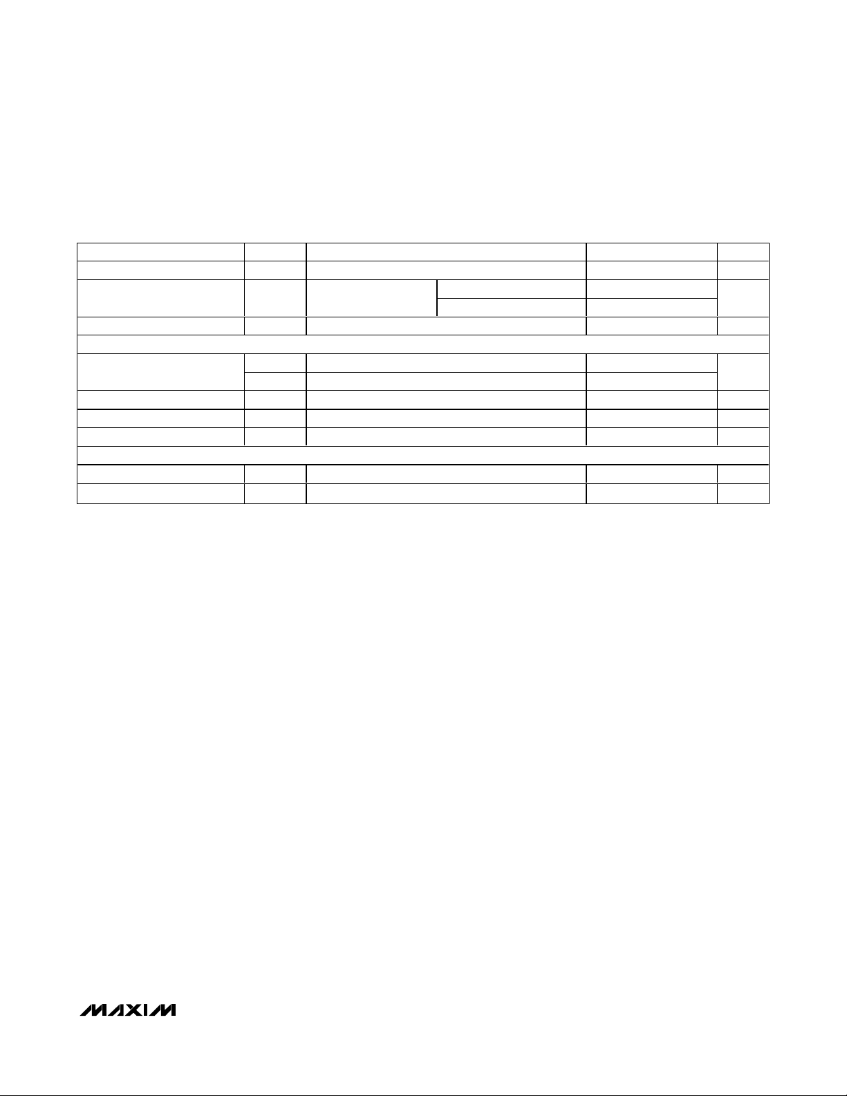
ELECTRICAL CHARACTERISTICS (continued)
(VIN= 14V, I
OUT
= 1mA, CIN= 0.1µF, C
OUT
= 2.2µF, TA= TJ= -40°C to +125°C, unless otherwise noted. Typical specifications are
at T
A
= +25°C.) (Note 1)
Output Current Limit 80 350 mA
Output Voltage Noise
Power-Supply Rejection Ratio PSRR f = 100Hz, V
ENABLE LOGIC
Enable Threshold Voltage
Enable Threshold Hysteresis 60 mV
Enable Pulldown Current Internally pulled down to GND 0.5 µA
Enable to Regulation Time (Note 5) 0.4 2 ms
THERMAL SHUTDOWN
Thermal Shutdown T
Thermal Shutdown Hysteresis T
PARAMETER SYMBOL CONDITIONS MIN TYP MAX UNITS
V
= 3.3V 115
OUT
= 500mV
OUT
V
= 5V 179
OUT
, I
P-P
= 50mA 66 dB
OUT
1.4
20 °C
V
IL
V
IH
SHDN
HYST
100Hz to 100kHz, I
= 50mA, C
Junction temperature rising +165 °C
= 2.2µF
OUT
IN_RIPPLE
0.4
µV
RMS
V
Page 4
MAX15006/MAX15007
40V, Ultra-Low Quiescent-Current
Linear Regulators in 6-Pin TDFN/8-Pin SO
4 _______________________________________________________________________________________
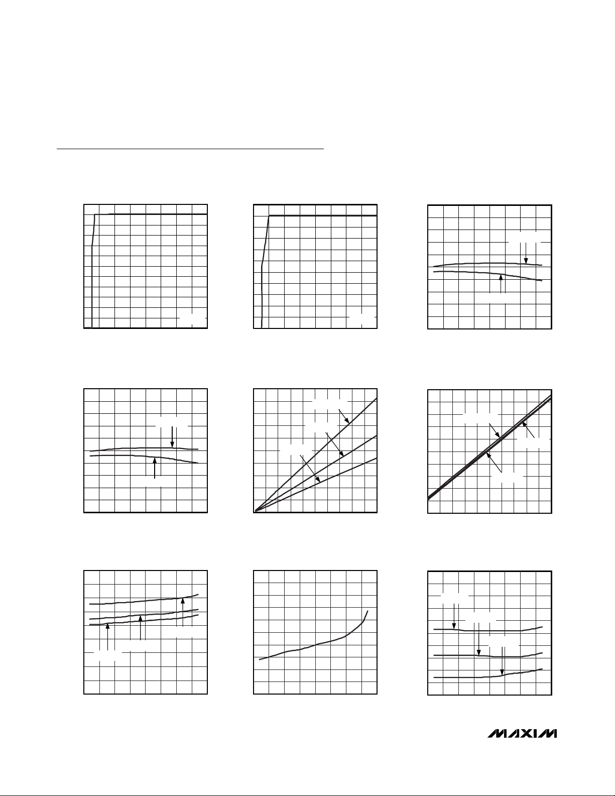
Typical Operating Characteristics
(VIN= 14V, CIN= 0.1µF, C
OUT
= 2.2µF, VEN= VIN, TA= +25°C, unless otherwise noted.)
OUTPUT VOLTAGE vs. INPUT VOLTAGE
(MAX15006A/MAX15007A)
MAX15006 toc01
VIN (V)
V
OUT
(V)
353020 2510 155
0.3
0.6
0.9
1.2
1.5
1.8
2.1
2.4
2.7
3.3
3.0
3.6
0
040
I
OUT
= 0
OUTPUT VOLTAGE vs. INPUT VOLTAGE
(MAX15006B/MAX15007B)
MAX15006 toc02
VIN (V)
V
OUT
(V)
353020 2510 155
0.5
1.0
1.5
2.0
2.5
3.0
3.5
4.0
4.5
5.0
5.5
0
040
I
OUT
= 0
OUTPUT VOLTAGE vs. TEMPERATURE
(MAX15006A/MAX15007A)
MAX15006 toc03
TEMPERATURE (°C)
V
OUT
(V)
12510050 750 25-25
3.18
3.21
3.24
3.27
3.30
3.33
3.36
3.39
3.42
3.45
3.15
-50 150
I
OUT
= 50mA
I
OUT
= 1mA
OUTPUT VOLTAGE vs. TEMPERATURE
(MAX15006B/MAX15007B)
MAX15006 toc04
TEMPERATURE (°C)
V
OUT
(V)
12510050 750 25-25
4.80
4.85
4.90
4.95
5.00
5.05
5.10
5.15
5.20
5.25
4.75
-50 150
I
OUT
= 50mA
I
OUT
= 1mA
DROPOUT VOLTAGE vs. LOAD CURRENT
(MAX15006B/MAX15007B)
MAX15006 toc05
I
OUT
(mA)
V
DROPOUT
(mV)
3530 454020 2510 155
50
100
150
200
250
300
350
400
450
500
0
050
TA = +125°C
TA = +25°C
TA = -40°C
GROUND CURRENT vs. LOAD CURRENT
(MAX15006B/MAX15007B)
MAX15006 toc06
I
OUT
(mA)
I
GND
(μA)
3530 454020 2510 155
10
20
30
40
50
60
70
80
90
100
0
050
TA = +125°C
TA = +25°C
TA = -40°C
GROUND CURRENT vs. TEMPERATURE
(I
OUT
= 0)
MAX15006 toc07
TEMPERATURE (°C)
I
GND
(μA)
12510050 75025-25
2
4
6
8
10
12
14
16
18
0
-50 150
VIN = +6V
VIN = +14V
VIN = +40V
GROUND CURRENT vs. TEMPERATURE
(I
OUT
= 50mA)
MAX15006 toc08
TEMPERATURE (°C)
I
GND
(μA)
12510050 75025-25
91
92
93
94
95
96
97
98
99
100
90
-50 150
SHUTDOWN SUPPLY CURRENT
vs. TEMPERATURE
MAX15006 toc09
TEMPERATURE (°C)
I
SHDN
(μA)
12510050 75025-25
1
2
3
4
5
6
7
8
9
10
0
-50 150
VIN = +40V
VIN = +14V
VIN = +6V
Page 5
MAX15006/MAX15007
40V, Ultra-Low Quiescent-Current
Linear Regulators in 6-Pin TDFN/8-Pin SO
_______________________________________________________________________________________
5
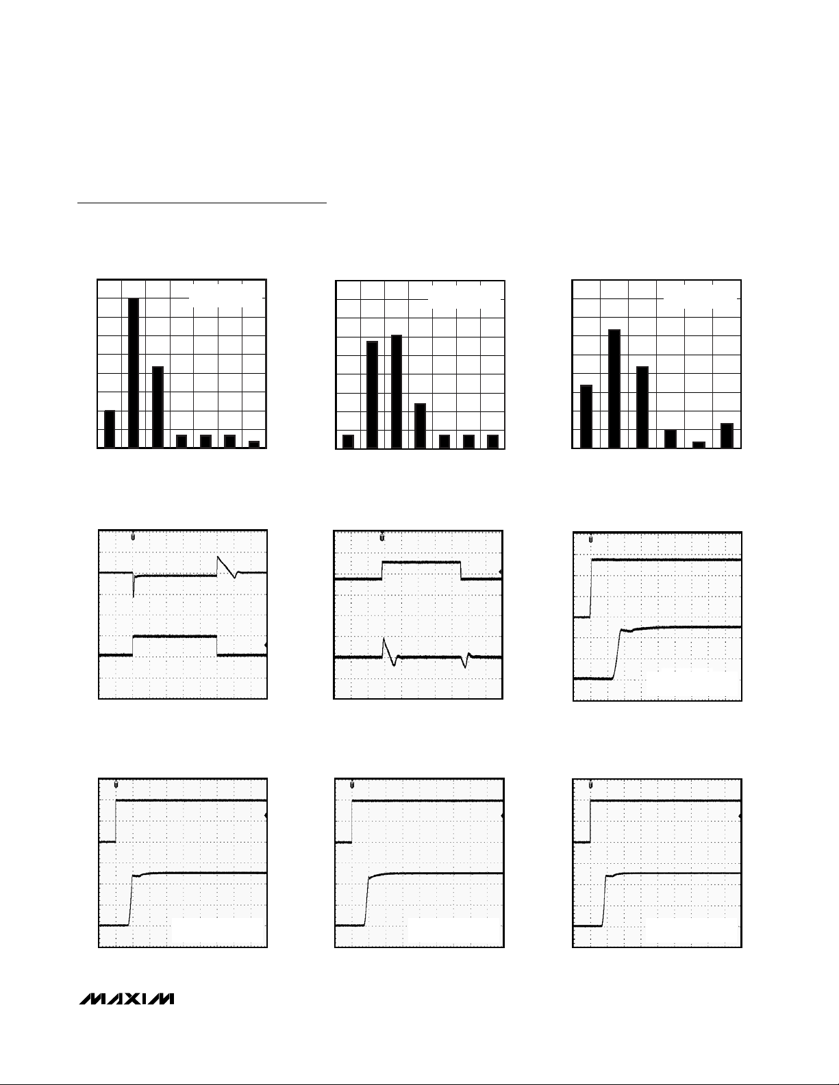
Typical Operating Characteristics (continued)
(VIN= 14V, CIN= 0.1µF, C
OUT
= 2.2µF, VEN= VIN, TA= +25°C, unless otherwise noted.)
GROUND CURRENT DISTRIBUTION
= -40°C)
(T
10.5
10.6
A
10.7
I
(μA)
GND
27
24
21
18
15
12
NUMBER OF UNITS
9
6
3
0
10.4
LOAD-TRANSIENT RESPONSE
(MAX15006B/MAX15007B)
MAX15007, I
50 UNITS TESTED
OUT
10.910.8
MAX15006 toc13
= 0
11.0
MAX15006 toc10
NUMBER OF UNITS
V
OUT
AC-COUPLED
200mV/div
GROUND CURRENT DISTRIBUTION
27
24
21
18
15
12
9
6
3
0
10.9
10.8
INPUT-VOLTAGE STEP RESPONSE
(MAX15006B/MAX15007B, I
(T
11.0
= +25°C)
A
11.1
I
(μA)
GND
MAX15007, I
50 UNITS TESTED
11.311.2
OUT
MAX15006 toc14
= 0
OUT
11.4
= 1mA)
MAX15006 toc11
18V
V
IN
14V
GROUND CURRENT DISTRIBUTION
(T
11.7
A
11.8
27
24
21
18
15
12
NUMBER OF UNITS
9
6
3
0
11.6
STARTUP RESPONSE
= +125°C)
MAX15007, I
50 UNITS TESTED
11.9
I
(μA)
GND
12.0
= 0
OUT
12.1
MAX15006 toc15
MAX15006 toc12
V
IN
5V/div
400μs/div
ENABLE STARTUP RESPONSE
MAX15006B/MAX15007B
= 0
I
OUT
400μs/div
MAX15006 toc16
50mA
I
OUT
1mA
EN
1V/div
V
OUT
2V/div
400μs/div
ENABLE STARTUP RESPONSE
MAX15006B/MAX15007B
= 50mA
I
OUT
400μs/div
MAX15006 toc17
V
OUT
AC-COUPLED
100mV/div
EN
1V/div
V
OUT
2V/div
MAX15006B/MAX15007B
= 1mA
I
OUT
200μs/div
ENABLE STARTUP RESPONSE
MAX15006B/MAX15007B
= 40V, I
V
IN
400μs/div
OUT
MAX15006 toc18
= 0
V
OUT
2V/div
EN
1V/div
V
OUT
2V/div
Page 6

MAX15006/MAX15007
40V, Ultra-Low Quiescent-Current
Linear Regulators in 6-Pin TDFN/8-Pin SO
6 _______________________________________________________________________________________
Typical Operating Characteristics (continued)
(VIN= 14V, CIN= 0.1µF, C
OUT
= 2.2µF, VEN= VIN, TA= +25°C, unless otherwise noted.)
ENABLE STARTUP RESPONSE
MAX15006B/MAX15007B
= 40V, I
V
IN
400μs/div
10
1
0.1
OUTPUT-NOISE SPECTRAL DENSITY (μV/√Hz)
0.01
0.01 100
OUT
MAX15006 toc19
= 50mA
EN
1V/div
V
OUT
2V/div
0
-10
-20
-30
-40
-50
PSRR (dB)
-60
-70
-80
-90
-100
OUTPUT-NOISE SPECTRAL DENSITY
vs. FREQUENCY
MAX15006B/MAX15007B
= 50mA
I
OUT
1100.1
FREQUENCY (kHz)
C
0.01 1000
POWER-SUPPLY REJECTION RATIO
vs. FREQUENCY
I
= 50mA
OUT
= 2.2μF
OUT
C
= 10μF
OUT
1001100.1
FREQUENCY (kHz)
150
135
MAX15006 toc22
)
(μV
e
RMS
n
120
105
90
75
60
45
30
15
0
OUTPUT-NOISE SPECTRAL DENSITY
vs. FREQUENCY
10
MAX15006 toc20
1
0.1
OUTPUT-NOISE SPECTRAL DENSITY (μV/√Hz)
0.01
0.01 100
FREQUENCY (kHz)
OUTPUT VOLTAGE NOISE
vs. LOAD CURRENT
MAX15006A/MAX15007A
05045
I
(mA)
OUT
403525 301510 205
MAX15006A/MAX15007A
= 50mA
I
OUT
1100.1
MAX15006 toc23
MAX15006 toc21
Page 7

MAX15006/MAX15007
40V, Ultra-Low Quiescent-Current
Linear Regulators in 6-Pin TDFN/8-Pin SO
_______________________________________________________________________________________ 7
Typical Operating Characteristics (continued)
(VIN= 14V, CIN= 0.1µF, C
OUT
= 2.2µF, VEN= VIN, TA= +25°C, unless otherwise noted.)
Pin Description
150
135
120
105
)
90
RMS
75
(μV
n
e
60
45
30
15
0
0221816 20
PIN
MAX15006 MAX15007
TDFN SO TDFN SO
1, 2 1 1, 2 1 IN
3
2, 3,
4, 6, 7
4 5 4 5 GND Ground
5, 6 8 5, 6 8 OUT
OUTPUT VOLTAGE NOISE
vs. OUTPUT CAPACITANCE
MAX15006A/MAX15007A
= 25mA
I
OUT
1412810462
C
(μF)
OUT
NAME FUNCTION
— 2, 4, 6, 7 N.C. No Connection. Not internally connected.
CLAMPED LOAD DUMP
= 0)
(I
OUT
MAX15006 toc24
100ms/div
MAX15006 toc25
40V
V
IN
13.5V
V
OUT
AC-COUPLED
20mV/div
Regulator Supply Input. Supply voltage ranges from 4V to 40V. Bypass
with a 0.1µF capacitor to GND.
Regulator Output. Bypass OUT to GND with a low-ESR capacitor with a
minimum 2.2µF.
Active-High Enable Input. Force EN high (or connect to V
—— 3 3 EN
regulator on. Pull EN low (or leave unconnected) to place the device in a
low-power shutdown mode. EN is internally pulled down to GND through a
0.5µA sink current.
Exposed Pad. Internally connected to GND. Connect EP to the ground
EP EP EP EP EP
plane for enhanced thermal performance. Do not use EP as a ground
connection.
) to turn the
IN
Page 8

MAX15006/MAX15007
40V, Ultra-Low Quiescent-Current
Linear Regulators in 6-Pin TDFN/8-Pin SO
8 _______________________________________________________________________________________
8 _______________________________________________________________________________________
Figure 1. MAX15006 Simplified Functional Diagram
Functional Diagrams
Figure 2. MAX15007 Simplified Functional Diagram
IN
THERMAL
SENSOR
GND
1.242V
IN
EN
CONTROL
LOGIC
THERMAL
SENSOR
1.242V
REF
REF
-
+
ERROR
AMPLIFIER
-
+
ERROR
AMPLIFIER
FET DRIVER
WITH
CURRENT LIMIT
MAX15006
FET DRIVER
WITH
CURRENT LIMIT
OUT
OUT
GND
MAX15007
Page 9

MAX15006/MAX15007
40V, Ultra-Low Quiescent-Current
Linear Regulators in 6-Pin TDFN/8-Pin SO
_______________________________________________________________________________________ 9
Detailed Description
The MAX15006/MAX15007 high-voltage linear regulators operate over a 4V to 40V input voltage range.
These devices guarantee 50mA load drive, and offer
preset output voltages of +3.3V or +5V. Thermal shutdown and short-circuit protection prevent damage during overtemperature and overcurrent conditions. The
MAX15007 includes an enable input (EN) allowing the
regulators to be turned on/off using a logic-level voltage. Driving EN high turns on the device while driving
EN low places the device in a low-power shutdown
mode. In shutdown, the supply current is reduced to
3µA (typ). The MAX15006/MAX15007 operate over the
-40°C to +125°C automotive temperature range. All
devices are available in thermally enhanced 6-pin
TDFN and 8-pin SO packages capable of dissipating
1.904W and 1.860W at T
A
= +70°C, respectively.
Regulator
The regulator accepts an input voltage from 4V to 40V.
The MAX15006A/MAX15007A have a fixed 3.3V output
voltage while the MAX15006B/MAX15007B offer a fixed
5V output voltage.
EN Input (MAX15007 Only)
EN is an active-high, logic-level enable input that turns
the device on or off. Drive EN high to turn the device
on. An internal 0.5µA pulldown current keeps the
MAX15007 in shutdown mode when driven by a three-
state driver in high-impedance mode, or an open-drain
driver. While in shutdown, the device consumes only
3µA (typ). EN withstands voltages up to 40V, allowing it
to be driven by high input level voltages or connected
to IN for always-on operation.
Thermal Protection
When the junction temperature exceeds +165°C, an
internal thermal sensor turns the pass transistor off, and
allows the device to cool. The thermal sensor turns the
pass transistor on again after the junction temperature
cools by 20°C. This results in a cycled output during
continuous thermal-overload conditions. Thermal protection protects the MAX15006/MAX15007 in the event
of fault conditions. Operation at TJ= +150°C without
going into thermal shutdown is not guaranteed. Use
Figures 3a and 3b to determine the minimum guaranteed output current.
Output Short-Circuit Current Limit
The MAX15006/MAX15007 feature a 175mA current
limit. The output can be shorted to GND for an indefinite period of time without damage to the device.
During a short circuit, the power dissipated across the
pass transistor can quickly heat the device. When the
die temperature reaches +165°C, the MAX15006/
MAX15007 shut down and automatically restart after
the die temperature cools by 20°C.
_______________________________________________________________________________________ 9
Figure 3a. Minimum Output Current vs. Ambient Temperature
(6-Pin TDFN-EP)
Figure 3b. Minimum Output Current vs. Ambient Temperature
(8-Pin SO-EP)
55
50
45
40
35
30
VIN = 26V, V
25
20
OUTPUT CURRENT (mA)
15
10
5
0
80 130
OUT
VIN = 26V, V
AMBIENT TEMPERATURE (°C)
= 5V
OUT
VIN = 18V, V
= 3.3V
OUT
VIN = 18V,
= 3.3V
V
OUT
= 5V
MAX15006 fig03a
125120110 11590 95 100 10585
55
50
45
40
35
30
25
VIN = 26V, V
20
OUTPUT CURRENT (mA)
15
10
5
0
VIN = 26V, V
80 130
AMBIENT TEMPERATURE (°C)
OUT
= 5V
OUT
= 3.3V
VIN = 18V, V
VIN = 18V,
V
OUT
OUT
= 3.3V
= 5V
MAX15006 fig03b
125120110 11590 95 100 10585
Page 10

MAX15006/MAX15007
40V, Ultra-Low Quiescent-Current
Linear Regulators in 6-Pin TDFN/8-Pin SO
10 ______________________________________________________________________________________
Applications Information
Available Output Current Calculation
The MAX15006/MAX15007 provide up to 50mA of continuous output current. The input voltage range extends
to 40V. Package power dissipation limits the amount of
output current available for a given input/output voltage
and ambient temperature. Figure 4 shows the maximum
allowable power dissipation for these devices to keep the
junction temperature below +150°C. Figure 4 assumes
that the exposed metal pad of the MAX15006/MAX15007
is soldered to 1in
2
of PCB copper.
Use Figure 4 to determine the allowable package dissipation for a given ambient temperature. Alternately, use
the following formulas to calculate the allowable package dissipation. For the TDFN package:
For the SO-EP package:
After determining the allowable package dissipation,
calculate the maximum allowable output current, without exceeding the +150°C junction temperature, using
the following formula:
The above equations do not include the negligible
power dissipation from self-heating due to the IC
ground current.
Example 1 (TDFN Package):
T
A
= +125°C
V
IN
= 26V
V
OUT
= 3.3V
Calculate the maximum allowable package dissipation
at the given temperature as follows:
And establish the maximum output current:
Example 2 (TDFN Package):
TA= +85°C
VIN= 14V
V
OUT
= 5V
Calculate the maximum allowable package dissipation
at the given temperature as follows:
Figure 4. Calculated Maximum Power Dissipation vs. Ambient
Temperature
(W)
P
2.4
1.9408W
2.2
(6-PIN TDFN)
2.0
1.8
1.8605W
1.6
(8-PIN SO-EP)
1.4
1.2
D
1.0
0.8
0.6
0.4
0.2
0
20
0
60
40
TEMPERATURE (°C)
DERATE
23.3mW/°C
80
DERATE
23.8mW/°C
100
120
MAX15006 fig04
140
.
1 8605 70
W for T C
⎧
⎪
PD
=
⎨
. . –
1 8605 0 0233 70 70 125
W
⎪
⎩
≤+ °
A
−
W
°
C
°
x T C for C T C
()
AA
+°< ≤+ °
P
I
OUT(MAX)
=
D
VV
−
IN OUT
≤
50mA
P 1.9048W 0.0238
=−
D
W
°
°− °
125 C 70 C 595.8mW
()
C
=
⎫
⎪
⎬
⎪
⎭
I
OUT(MAX)
.
1 9048 70
W for T C
⎧
⎪
PD
=
⎨
. . –
1 9048 0 0238 70 70 125
W
⎪
⎩
≤+ °
A
−
W
x T C for C T C
°
C
°
()
AA
+°< ≤+ °
⎫
⎪
⎬
⎪
⎭
P 1.9048W 0.0238
=−°°− °
D
595.8mW
=
26V 3.3V
−
W
85 C 70 C 1.5478W
()
C
=
26.2mA
=
Page 11

MAX15006/MAX15007
40V, Ultra-Low Quiescent-Current
Linear Regulators in 6-Pin TDFN/8-Pin SO
______________________________________________________________________________________ 11
Then determine the maximum output current:
Example 3 (TDFN Package):
T
A
= +50°C
V
IN
= 9V
V
OUT
= 5V
Calculate the maximum allowable package dissipation
at the given temperature as follows:
P
D
= 1.9048W
Find the maximum output current:
In Examples 2 and 3, the maximum output current is
calculated as 172mA and 476mA, respectively; however, the allowable output current cannot exceed 50mA.
Alternately, use Figures 5a and 5b to quickly determine
the maximum allowable output current for selected
ambient temperatures and input voltages.
Output-Capacitor Selection
and Regulator Stability
For stable operation over the full temperature range
and with load currents up to 50mA, use a low-ESR
2.2µF (min) ceramic or tantalum output capacitor. Use
larger output-capacitor values such as 22µF to reduce
noise, improve load-transient response, and powersupply rejection.
Some ceramic dielectrics exhibit large capacitance
and ESR variations with temperature. Ensure the minimum capacitance under worst-case conditions does
not drop below 1.3µF to ensure output stability. With an
X7R dielectric, 2.2µF should be sufficient at all operating temperatures.
Figure 5a. Calculated Maximum Output Current vs. Input
Voltage (6-Pin TDFN-EP)
Figure 5b. Calculated Maximum Output Current vs. Input
Voltage (8-Pin SO-EP)
I
OUT(MAX)
1.5478W
=
14V 5V
=⇒ =ImA
−
172mA
()
OUT MAX
50
I
OUT(MAX)
1.9048W
=
9V 5V
=⇒ =ImA
−
476mA
()
OUT MAX
50
60
55
50
45
40
35
(mA)
30
25
OUT(MAX)
I
20
15
10
5
0
TA = +125°C
V
= 5V
OUT
6-PIN TDFN
040
TA = +70°C
TA = +85°C
VIN (V)
MAX15006 fig05a
353020 2510 155
60
55
50
45
40
35
(mA)
30
25
OUT(MAX)
I
20
15
10
5
0
TA = +125°C
V
= 5V
OUT
8-PIN SO-EP
040
TA = +70°C
TA = +85°C
VIN (V)
MAX15006 fig05b
353020 2510 155
Page 12

MAX15006/MAX15007
40V, Ultra-Low Quiescent-Current
Linear Regulators in 6-Pin TDFN/8-Pin SO
12 ______________________________________________________________________________________
Selector Guide
TOP VIEW
IN
OUT GND
ENIN
OUT
MAX15007A
MAX15007B
123
654
TDFN
+
+
N.C.
GND
*EXPOSED PAD
*EP
*EP
N.C.
1
2
87OUT
N.C.N.C.
EN
IN
SO
3
4
6
5
MAX15007A
MAX15007B
Pin Configurations (continued)
Ordering Information (continued)
Note: All devices are specified over the -40°C to +125°C operating temperature range.
+
Denotes lead-free package.
*
EP = Exposed pad.
Chip Information
PROCESS: BiCMOS
PART ENABLE INPUT
MAX15006AASA+ — 3.3 — 8 SO-EP
MAX15006AATT+ — 3.3 APE 6 TDFN-EP
MAX15006BASA+ — 5 — 8 SO-EP
MAX15006BATT+ — 5 APF 6 TDFN-EP
MAX15007AASA+ √ 3.3 — 8 SO-EP
MAX15007AATT+ √ 3.3 APG 6 TDFN-EP
MAX15007BASA+ √ 5 — 8 SO-EP
MAX15007BATT+ √ 5 APH 6 TDFN-EP
FIXED OUTPUT
VOLTAGE (V)
TOP MARK PIN-PACKAGE
PART
MAX15007AASA+ 8 SO-EP* — S8E-12
MAX15007AATT+ 6 TDFN-EP* APG T633-2
MAX15007BASA+ 8 SO-EP* — S8E-12
MAX15007BATT+ 6 TDFN-EP* APH T633-2
PINPACKAGE
TOP
MARK
PKG
CODE
Page 13

MAX15006/MAX15007
Package Information
(The package drawing(s) in this data sheet may not reflect the most current specifications. For the latest package outline information,
go to www.maxim-ic.com/packages
.)
40V, Ultra-Low Quiescent-Current
Linear Regulators in 6-Pin TDFN/8-Pin SO
______________________________________________________________________________________ 13
6, 8, &10L, DFN THIN.EPS
PACKAGE OUTLINE, 6,8,10 & 14L,
TDFN, EXPOSED PAD, 3x3x0.80 mm
21-0137
1
H
2
Page 14

MAX15006/MAX15007
40V, Ultra-Low Quiescent-Current
Linear Regulators in 6-Pin TDFN/8-Pin SO
14 ______________________________________________________________________________________
Package Information (continued)
(The package drawing(s) in this data sheet may not reflect the most current specifications. For the latest package outline information,
go to www.maxim-ic.com/packages
.)
COMMON DIMENSIONS
SYMBOL
MIN. MAX.
A 0.70 0.80
D 2.90 3.10
E 2.90 3.10
0.00 0.05
A1
L 0.20 0.40
0.25 MIN.k
A2 0.20 REF.
PACKAGE VARIATIONS
PKG. CODE N D2 E2 e JEDEC SPEC b [(N/2)-1] x e
T633-2 6 1.50±0.10 2.30±0.10
T833-2 8 1.50±0.10 2.30±0.10 0.65 BSC MO229 / WEEC 0.30±0.05 1.95 REF
T833-3 8 1.50±0.10 2.30±0.10 0.65 BSC MO229 / WEEC 0.30±0.05 1.95 REF
1.50±0.10
1.50±0.10
1.50±0.1010T1033-2
2.30±0.101.50±0.106T633-1 0.95 BSC MO229 / WEEA 1.90 REF0.40±0.05
0.40±0.05 1.90 REF
2.30±0.10
0.95 BSC MO229 / WEEA
MO229 / WEEC
MO229 / WEED-3
0.50 BSC
0.40 BSC - - - - 0.20±0.05 2.40 REFT1433-2 14 2.30±0.101.70±0.10
MO229 / WEED-3
1.95 REF0.30±0.050.65 BSC2.30±0.108T833-1
2.00 REF0.25±0.050.50 BSC2.30±0.1010T1033-1
2.00 REF0.25±0.05
2.40 REF0.20±0.05- - - - 0.40 BSC1.70±0.10 2.30±0.1014T1433-1
PACKAGE OUTLINE, 6,8,10 & 14L,
TDFN, EXPOSED PAD, 3x3x0.80 mm
-DRAWING NOT TO SCALE-
21-0137
2
H
2
Page 15

MAX15006/MAX15007
40V, Ultra-Low Quiescent-Current
Linear Regulators in 6-Pin TDFN/8-Pin SO
Maxim cannot assume responsibility for use of any circuitry other than circuitry entirely embodied in a Maxim product. No circuit patent licenses are
implied. Maxim reserves the right to change the circuitry and specifications without notice at any time.
Maxim Integrated Products, 120 San Gabriel Drive, Sunnyvale, CA 94086 408-737-7600 ____________________
15
© 2006 Maxim Integrated Products is a registered trademark of Maxim Integrated Products, Inc.
Heaney
Package Information (continued)
(The package drawing(s) in this data sheet may not reflect the most current specifications. For the latest package outline information,
go to www.maxim-ic.com/packages
.)
8L, SOIC EXP. PAD.EPS
PACKAGE OUTLINE
8L SOIC, .150" EXPOSED PAD
21-0111
1
C
1
 Loading...