

Page 1
19-5033; Rev 0; 10/09
Two-Lane and Four-Lane DisplayPort Passive
Switches with Separate AUX/HPD Control
General Description
The MAX4998/MAX14998 high-speed passive switches
route DisplayPort™ between two possible destinations
or vice versa in laptops or desktop PCs. The MAX4998/
MAX14998 are intended to be used where ultra-highspeed performance and minimal input capacitance is
required.
The MAX4998 has three double-pole/double-throw
(DPDT) switches and one single-pole/double-throw
(SPDT) switch. Two DPDT switches are for high-frequency switching, one DPDT switch is for AUX, and the one
SPDT switch is for HPD. The two high-frequency switches
are selected by SEL1, and the AUX and HPD are selected
by SEL2. This part is suitable for two-lane DisplayPort
switching.
The MAX14998 has six double-pole/double-throw (DPDT)
switches. Four DPDT switches are for high-frequency
switching, and two DPDT switches are for AUX and HPD.
The four high-frequency switches are selected by SEL1,
and the AUX and HPD are selected by SEL2. This part is
suitable for four-lane DisplayPort switching.
The MAX4998/MAX14998 are fully specified to operate
from a single +3.3V (typ) power supply. The MAX4998
is available in a 3.5mm x 5.5mm, 28-pin TQFN package
with exposed pad, and the MAX14998 is available in a
3.5mm x 9mm, 42-pin TQFN package with exposed pad.
Both devices operate over the -40NC to +85NC extended
temperature range.
Applications
Notebook PCs
Desktop PCs
Features
S Single 3.3V Power-Supply Voltage
S 5GHz Bandwidth
S Support 1.6/2.7Gbps DisplayPort Signals
S Excellent Return Loss -14dB at 1.35GHz
S Independent High Frequency: AUX Select
S Designed for AC-Coupled Circuits
S Pass Throughs Are Maintained
S Low 850µA (max) Supply Current
S Small Packages
3.5mm x 5.5mm, 28-Pin TQFN Package with
Exposed Pad
3.5mm x 9mm, 42-Pin TQFN Package with
Exposed Pad
S Flow-Through Layout for Easy Board Layout
S ESD Protection for All I/O Pins: Human Body
Model (HBM) Q4kV
Ordering Information
PART TEMP RANGE PIN-PACKAGE
MAX4998ETI+T
MAX14998ETO+T*
+Denotes a lead(Pb)-free/RoHS-compliant package.
T = Tape and reel.
*Future Product. Contact factory for availability.
**EP = Exposed Pad.
Typical Operating Circuit appears at end of data sheet.
-40NC to +85NC
-40NC to +85NC
28 TQFN-EP**
42 TQFN-EP**
MAX4998/MAX14998
DisplayPort is a trademark of Video Electronics Standards
Association (VESA).
_______________________________________________________________ Maxim Integrated Products 1
For pricing, delivery, and ordering information, please contact Maxim Direct at 1-888-629-4642,
or visit Maxim’s website at www.maxim-ic.com.
Page 2
Two-Lane and Four-Lane DisplayPort Passive
Switches with Separate AUX/HPD Control
ABSOLUTE MAXIMUM RATINGS
(All voltages referenced to GND, unless otherwise noted.)
VDD ..........................................................................-0.3V to +4V
SEL1, SEL2, COM_, NO_, NC_ (Note 1) .....-0.3V to +(VDD + 0.3)V
|V
COM_
- V
NO_|, |VCOM_
- V
| (Note 1) .....................0 to +2V
NC_
Continuous Current (COM_ to NO_/NC_) ....................... Q70mA
Peak Current (COM_ to NO_/NC_)
(pulsed at 1ms, 10% duty cycle) ................................. Q70mA
Continuous Current (SEL1, SEL2) ................................... Q30mA
Peak Current (SEL1, SEL2)
(pulsed at 1ms, 10% duty cycle) ................................. Q70mA
Continuous Power Dissipation (TA = +70NC)
28-Pin TQFN (derate 28.6mW/NC above +70NC) ....... 2285mW
42-Pin TQFN (derate 34.5mW/NC above +70NC) ....... 2758mW
Note 1: Signals on COM_, NO_, NC_, SEL1, and SEL2 exceeding VDD or GND are clamped by internal diodes. Limit forward-
diode current to the maximum current rating.
Note 2: Package thermal resistances were obtained using the method described in JEDEC specification JESD51-7, using a
4-layer board. For detailed information on package thermal considerations, refer to www.maxim-ic.com/thermal-tutorial.
MAX4998/MAX14998
Stresses beyond those listed under “Absolute Maximum Ratings” may cause permanent damage to the device. These are stress ratings only, and functional
operation of the device at these or any other conditions beyond those indicated in the operational sections of the specifications is not implied. Exposure to absolute
maximum rating conditions for extended periods may affect device reliability.
Operating Temperature Range .......................... -40NC to +85NC
Junction Temperature .....................................................+150NC
Storage Temperature Range ............................ -65NC to +150NC
Package Junction-to-Ambient Thermal Resistance (BJA) (Note 2)
28-Pin TQFN .................................................................35NC/W
42-Pin TQFN .................................................................29NC/W
Package Junction-to-Case Thermal Resistance (BJC) (Note 2)
28-Pin TQFN ................................................................2.7NC/W
42-Pin TQFN ...................................................................2NC/W
Lead Temperature (soldering, 10s) ................................+300NC
ELECTRICAL CHARACTERISTICS
(VDD = +3.3V Q10%, TA = T
noted.) (Note 3)
PARAMETER SYMBOL CONDITIONS MIN TYP MAX UNITS
ANALOG SWITCH
Analog Signal Range
Voltage Between COM_ and
NO_/NC_
On-Resistance R
On-Resistance Match
Between Pairs of Same
Channel
On-Resistance Match
Between Channels
On-Resistance Flatness R
NO_ or NC_ Off-Leakage
Current
COM_ On-Leakage
Current
DIGITAL SIGNALS
SEL1 and SEL2 to Switch
Turn-On Time
MIN
to T
|V
unless otherwise noted. Typical values are at VDD = +3.3V, TA = +25NC, unless otherwise
MAX,
V
, V
NC_
- V
- V
ON
ON
ON
NO_
NO_|,
NC_
,
COM_
COM_
|V
COM_
DR
DR
FLAT(ON)
I
NO_(OFF)
I
NC_(OFF)
I
COM_(ON)
t
ON_SEL
V
|
I
= 15mA;
COM_
V
NO_, VNC_
= 0V, +1.2V
VDD = +3.0V; I
V
= 0V (Notes 4, 5)
NC_
VDD = +3.0V; I
V
= 0V (Notes 4, 5)
NC_
VDD = +3.0V; I
V
= 0V, +1.2V (Notes 5, 6)
NC_
VDD = +3.6V; V
V
or V
NO_
NC_
VDD = +3.6V; V
V
or V
V
NO_
NO_
or V
NC_
NC_
CL = 100pF (Figure 1)
= 15mA; V
COM_
= 15mA; V
COM_
= 15mA; V
COM_
= 0V, +1.2V;
COM_
= +1.2V, 0V
= 0V, +1.2V;
COM_
= V
or unconnected
COM_
= +1.0V, RL = 50I,
NO_,
NO_,
NO_,
(VDD -
1.8)
0 1.8 V
7
0.1 2
1.0 4
0.3 1.5
-1 1
-1 1
45 120 ns
V
I
I
I
I
FA
FA
2 ______________________________________________________________________________________
Page 3
Two-Lane and Four-Lane DisplayPort Passive
Switches with Separate AUX/HPD Control
ELECTRICAL CHARACTERISTICS (continued)
(VDD = +3.3V Q10%, TA = T
noted.) (Note 3)
PARAMETER SYMBOL CONDITIONS MIN TYP MAX UNITS
SEL1 and SEL2 to Switch
Turn-Off Time
Differential Insertion Loss S
Differential Crosstalk S
Differential Return Loss S
Signal Data Rate BR
Differential -3dB Bandwidth f
Differential Off-Isolation S
LOGIC INPUT (SEL1, SEL2)
Input Logic-High V
Input Logic-Low V
Input Logic Hysteresis V
Input Leakage Current I
POWER SUPPLY
Power-Supply Range V
VDD Supply Current I
Note 3: All units are 100% production tested at TA = +85NC. Limits over the operating temperature range are guaranteed by
design and characterization and are not production tested.
Note 4: DRON = R
ON(MAX)
Note 5: Guaranteed by design. Not production tested.
Note 6: Flatness is defined as the difference between the maximum and minimum value of on-resistance as measured over the
specified analog signal range.
MIN
- R
to T
MAX,
ON(MIN)
unless otherwise noted. Typical values are at VDD = +3.3V, TA = +25NC, unless otherwise
t
OFF_SEL
DD21
DDCTK
DD11
-3BW
DD21_OFF
IH
IL
HYST
IN
DD
DD
or V
NO_
CL = 100pF (Figure 1)
f = 0.8GHz (Figure 2) -0.67
f = 1.35GHz (Figure 2) -0.95
f = 0.8GHz (Figure 2) -37
f = 1.35GHz (Figure 2) -34
f = 0.8GHz (Figure 2) -20
f = 1.35GHz (Figure 2) -14
RS = RL = 100I balanced
RS = RL = 100I balanced
f = 1.35GHz (Figure 2) -28 dB
V
= 0V or V
SEL_
V
= 0V or V
SEL_
= +1.0V, RL = 50I,
NC_
DD
DD
5 50 ns
17 Gbps
8.5 GHz
1.4 V
0.5 V
100 mV
-1 +1
3.0 3.6 V
500 850
V
.
dB
dB
dB
FA
FA
MAX4998/MAX14998
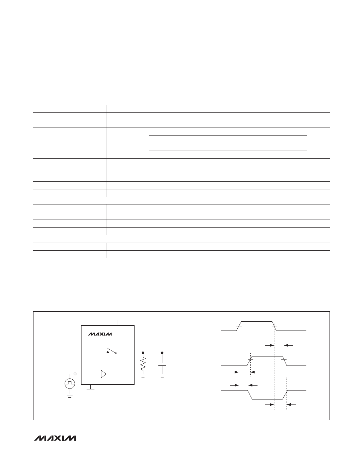
Test Circuits/Timing Diagrams
tr < 5ns
t
< 5ns
f
0.9 x V
0.9 x V
t
OFF _SEL
OUT
t
ON_ SEL
OUT
NO_ OR NC_
V
N_
SEL_
LOGIC
INPUT
SEL
C
INCLUDES FIXTURE AND STRAY CAPACITANCE.
L
V
OUT
Figure 1. Switching Time
_______________________________________________________________________________________ 3
MAX4998/MAX14998
GND
R
N_
( )
RL + R
L
ON
= V
+3.3V
V
DD
COM_
V
INPUT
SEL_
IH
V
IL
0V
0V
V
50%
OUT
0.9 x V
0.9 x V
OUT
t
ON_ SEL
t
OFF _SEL
OUT
LOGIC
V
OUT
R
L
C
L
SWITCH
OUTPUT
COM_
SWITCH
OUTPUT
COM_
Page 4

Two-Lane and Four-Lane DisplayPort Passive
Switches with Separate AUX/HPD Control
Test Circuits/Timing Diagrams (continued)
+3.3V
0.1µF
V
SEL1
0V
SEL20V
50Ω
NO_+
50Ω
NO_-
MAX4998/MAX14998
DD
COM_+
MAX4998
MAX14998
DIFFERENTIAL INSERTION LOSS/DIFFERENTIAL RETURN LOSS
COM_-
NC_+
NC_-
GND
DIFFERENTIAL INSERTION LOSS = 20log
0V OR V
50Ω
50Ω
50Ω
50Ω
DD
DD
PORT 1
V
IN+
PORT 2
V
IN-
PORT 3
V
OUT+
PORT 4
V
OUT-
SEL1
SEL20V OR V
COM_+
COM_-
NO_+/NC_+
NO_-/NC_-
( )
MAX4998
MAX14998
NETWORK
ANALYZER
50Ω
50Ω
50Ω
50Ω
V
OUT+
V
IN+
+3.3V
V
DD
GND
- V
OUT-
- V
IN-
0.1µF
COM_+
COM_-
NO_+/NC_+
NO_-/NC_-
V
50Ω
50Ω
PORT 1
V
IN+
PORT 2
V
IN-
PORT 3
V
OUT+
PORT 4
V
OUT-
+3.3V
0.1µF
NETWORK
V
SEL1
DD
SEL2V
DD
NO_+
NO_-
DD
COM_+
MAX4998
NETWORK
ANALYZER
50Ω
50Ω
50Ω
50Ω
MAX14998
COM_-
NC_+
NC_-
GND
DIFFERENTIAL OFF-ISOLATION
DIFFERENTIAL OFF-ISOLATION = 20log
PORT 1
V
IN+
PORT 2
V
IN-
PORT 3
V
OUT+
PORT 4
V
OUT-
ANALYZER
50Ω
50Ω
50Ω
50Ω
V
- V
OUT+
( )
OUT-
V
- V
IN+
IN-
DIFFERENTIAL CROSSTALK
V
- V
OUT+
DIFFERENTIAL CROSSTALK = 20log
MEASUREMENTS ARE STANDARDIZED AGAINST SHORTS AT IC TERMINALS.
DIFFERENTIAL OFF-ISOLATION IS MEASURED BETWEEN COM_ AND “OFF” NO_ OR NC_ TERMINAL ON EACH SWITCH.
DIFFERENTIAL ON-LOSS IS MEASURED BETWEEN COM_ AND “ON” NO_ OR NC_ TERMINAL ON EACH SWITCH.
DIFFERENTIAL CROSSTALK IS MEASURED BETWEEN ANY TWO PAIRS.
OUT-
( )
V
- V
IN+
IN-
Figure 2. Differential On-Loss, Differential Off-Isolation, and Differential Crosstalk
4 ______________________________________________________________________________________
Page 5

Two-Lane and Four-Lane DisplayPort Passive
DIFFERENTIAL RETURN LOSS (dB)
DIFFERENTIAL CROSSTALK (dB)
DIFFERENTIAL OFF-ISOLATION (dB)
DIFFERENTIAL INSERTION LOSS (dB)
Switches with Separate AUX/HPD Control
Typical Operating Characteristics
(T
= +25°C, unless otherwise noted.)
A
MAX4998/MAX14998
ON-RESISTANCE vs. COM_ VOLTAGE
8.0
VDD = 3.6V
I
= 15mA
COM_
7.5
7.0
6.5
6.0
5.5
ON-RESISTANCE (Ω)
5.0
4.5
4.0
-0.1 1.9
V
(V)
COM_
LOGIC THRESHOLD vs. SUPPLY VOLTAGE
1.5
VDD = 3.3V
1.3
V
IH
1.1
0.9
LOGIC THRESHOLD (V)
0.7
0.5
3.0 3.6
SUPPLY VOLTAGE (V)
V
IL
3.53.43.33.23.1
1.71.50.1 0.3 0.5 0.9 1.10.7 1.3
10
9
MAX4998/MAX14998 toc01
MAX4998/MAX14998 toc04
8
7
6
ON-RESISTANCE (Ω)
5
4
60
50
40
30
20
TURN-ON/OFF TIME (ns)
10
0
ON-RESISTANCE vs. COM_ VOLTAGE
VDD = 3.3V
= 15mA
I
COM_
TA = +85°C
TA = +25°C
TA = -40°C
-0.1 1.5
V
(V)
COM_
1.31.10.90.70.50.30.1
TURN-ON/OFF TIME vs. SUPPLY VOLTAGE
t
ON_SEL
t
OFF_SEL
3.0 3.6
SUPPLY VOLTAGE (V)
3.53.43.33.23.1
800
700
600
MAX4998/MAX14998 toc02
500
400
300
SUPPLY CURRENT (µA)
200
100
0
0
-1
-2
-3
MAX4998/MAX14998 toc05
-4
-5
-6
-7
-8
-9
-10
SUPPLY CURRENT vs. TEMPERATURE
VDD = 3.3V
-40 85
TEMPERATURE (°C)
6035-15 10
DIFFERENTIAL INSERTION LOSS
10 10,000
FREQUENCY (MHz)
1000100
MAX4998/MAX14998 toc03
MAX4998/MAX14998 toc06
0
-10
-20
-30
-40
-50
-60
-70
-80
10 10,000
DIFFERENTIAL OFF-ISOLATION
1000100
FREQUENCY (MHz)
_______________________________________________________________________________________ 5
0
-10
-20
MAX4998/MAX14998 toc07
-30
-40
-50
-60
-70
-80
DIFFERENTIAL CROSSTALK
10 10,000
FREQUENCY (MHz)
1000100
0
-5
-10
MAX4998/MAX14998 toc08
-15
-20
-25
-30
-35
-40
DIFFERENTIAL RETURN LOSS
10 10,000
FREQUENCY (MHz)
1000100
MAX4998/MAX14998 toc09
Page 6

Two-Lane and Four-Lane DisplayPort Passive
Switches with Separate AUX/HPD Control
Pin Configurations
TOP VIEWS
VDDNC3+
NC2-
NC2+
VDDNO1-
NO1+
NO0-
NO0+
GND
24 23 22 21 20 19 18 17 16 15
NO2+
NO1-
NO1+
NO0-
NO0+
NC3-
NC3+
NC2-
NC2+
38 37 36 35 34 33 32 31 30 29 28 27 26 25 24 23 22
NO2-
NO3+
NO3-
VDDNC4+
NC4-
NC5+
NC5-
25
NC1-
26
NC1+
27
NC0-
28
NC0+
+
1 2 3 4 5 6 7 8 9 10
COM0+
MAX4998 MAX14998
DD
V
COM2-
COM1-
COM0-
COM1+
COM2+
TQFN
MAX4998/MAX14998
*CONNECT EXPOSED PAD TO GROUND.
14
NO2+
NO2-
13
12
NO3+
*EP *EP
11
SEL2
DD
V
SEL1
COM3+
39
NC1-
40
NC1+
41
NC0-
42
NC0+
+
1 2 3 4 5 6 7 8 9 10 11 12 13 14 15 16 17
COM1+
COM1-
DD
V
COM2+
COM2-
COM3+
COM3-
COM4+
DD
V
COM0-
COM0+
COM4-
DD
V
COM5+
TQFN
COM5-
SEL1
21
20
19
18
SEL2
Pin Description
PIN
MAX4998 MAX14998
1 2 COM0+ Analog Switch 1. Common positive terminal.
2 3 COM0- Analog Switch 1. Common negative terminal.
3 4 COM1+ Analog Switch 2. Common positive terminal.
4 5 COM1- Analog Switch 2. Common negative terminal.
5 7 COM2+ Analog Switch 3. Common positive terminal.
6 8 COM2- Analog Switch 3. Common negative terminal.
7, 9, 15, 19 1, 6, 13, 26 V
8 9 COM3+ Analog Switch 4. Common positive terminal.
10 16 SEL1 Control Signal Input. Selects high-frequency switching.
11 17 SEL2 Control Signal Input. Selects AUX/HPD.
12 28 NO3+ Analog Switch 4. Normally Open positive terminal.
13 29 NO2- Analog Switch 3. Normally Open negative terminal.
14 30 NO2+ Analog Switch 3. Normally Open positive terminal.
16 36 NC3+ Analog Switch 4. Normally Closed positive terminal.
17 37 NC2- Analog Switch 3. Normally Closed negative terminal.
18 38 NC2+ Analog Switch 3. Normally Closed positive terminal.
20 31 NO1- Analog Switch 2. Normally Open negative terminal.
21 32 NO1+ Analog Switch 2. Normally Open positive terminal.
22 33 NO0- Analog Switch 1. Normally Open negative terminal.
NAME FUNCTION
Positive Supply Voltage Input. Connect VDD to a +3.0V to +3.6V supply voltage.
DD
Bypass VDD to GND with a 0.1mF ceramic capacitor placed as close to the device as
possible (see the Board Layout section).
NO4+
NO4-
NO5+
NO5-
6 ______________________________________________________________________________________
Page 7

Two-Lane and Four-Lane DisplayPort Passive
Switches with Separate AUX/HPD Control
Pin Description (continued)
MAX4998/MAX14998
PIN
MAX4998 MAX14998
23 34 NO0+ Analog Switch 1. Normally Open positive terminal.
24 — GND Ground
25 39 NC1- Analog Switch 2. Normally Closed negative terminal.
26 40 NC1+ Analog Switch 2. Normally Closed positive terminal.
27 41 NC0- Analog Switch 1. Normally Closed negative terminal.
28 42 NC0+ Analog Switch 1. Normally Closed positive terminal.
— 10 COM3- Analog Switch 4. Common negative terminal.
— 11 COM4+ Analog Switch 5. Common positive terminal.
— 12 COM4- Analog Switch 5. Common negative terminal.
— 14 COM5+ Analog Switch 6. Common positive terminal.
— 15 COM5- Analog Switch 6. Common negative terminal.
— 18 NO5- Analog Switch 6. Normally open negative terminal.
— 19 NO5+ Analog Switch 6. Normally open positive terminal.
— 20 NO4- Analog Switch 5. Normally open negative terminal.
— 21 NO4+ Analog Switch 5. Normally open positive terminal.
— 22 NC5- Analog Switch 6. Normally Closed negative terminal.
— 23 NC5+ Analog Switch 6. Normally Closed positive terminal.
— 24 NC4- Analog Switch 5. Normally Closed negative terminal.
— 25 NC4+ Analog Switch 5. Normally Closed positive terminal.
— 27 NO3- Analog Switch 4. Normally Open negative terminal.
— 35 NC3- Analog Switch 4. Normally Closed negative terminal.
— — EP
NAME FUNCTION
Exposed Pad. Internally connected to GND. Connect to a large plane to maximize
thermal performance. Not intended as an electrical part.
Detailed Description
The MAX4998/MAX14998 high-speed passive switches
route one DisplayPort source between two possible
destinations or vice versa. The MAX4998 is used to
switch two-lanes plus AUX/HPD DisplayPort, and the
MAX14998 is used to switch four-lanes plus AUX/HPD
DisplayPort.
The MAX4998/MAX14998 feature two digital control
inputs (SEL1, SEL2) to switch signal paths.
Digital Control Inputs (SEL1, SEL2)
The MAX4998/MAX14998 provide two digital control
inputs (SEL1, SEL2) to select the signal path between
the COM_ and NO_/NC_ channels. SEL1 selects highfrequency switching, while SEL2 selects AUX/HPD. On
the MAX4998, switches 1 and 2 are high-frequency
_______________________________________________________________________________________ 7
switches and switches 3 and 4 are both low-frequency
switches. On the MAX14998, switches 1, 2, 3, and 4 are
high-frequency switches and switches 5 and 6 are lowfrequency switches. The truth tables for the MAX4998/
MAX14998 are depicted in the Functional Diagrams/
Truth Tables. Drive SEL_ 0V to VDD to minimize power
consumption.
Analog Signal Levels
The MAX4998/MAX14998 accept standard DisplayPort
signals to a maximum of (VDD - 1.8V). Signals on the
COM_+ channels are routed to either the NO_+ or NC_+
channels. Signals on the COM_- channels are routed
to either the NO_- or NC_- channels. The MAX4998/
MAX14998 are bidirectional switches, allowing COM_,
NO_, and NC_, to be used as either inputs or outputs.
Page 8

Two-Lane and Four-Lane DisplayPort Passive
Switches with Separate AUX/HPD Control
Functional Diagrams/Truth Tables
V
DD
MAX14998
COM0+
COM0-
COM1+
COM1-
MAX4998/MAX14998
COM2+
COM2-
COM3+
COM3-
COM4+
COM4-
COM5+
COM5-
SEL1
SEL2
NC0+
NC0-
NO0+
NO0-
NC1+
NC1-
NO1+
NO1-
NC2+
NC2-
NO2+
NO2-
NC3+
NC3-
NO3+
NO3-
NC4+
NC4-
NO4+
NO4-
NC5+
NC5-
NO5+
NO5-
COM0+
COM0-
COM1+
COM1-
COM2+
COM2-
COM3+
SEL1
SEL2
V
DD
MAX4998
NC0+
NC0-
NO0+
NO0-
NC1+
NC1-
NO1+
NO1-
NC2+
NC2-
NO2+
NO2-
NC3+
NO3+
GND
SEL1 EVENT SWITCH
0 COM_ TO NC_ 1, 2, 3, 4
1 COM_ TO NO_ 1, 2, 3, 4
SEL2 EVENT SWITCH
0 COM_ TO NC_ 5, 6
1 COM_ TO NO_ 5, 6
SEL1 EVENT SWITCH
0 COM_ TO NC_ 1, 2
1 COM_ TO NO_ 1, 2
SEL2 EVENT SWITCH
0 COM_ TO NC_ 3, 4
1 COM_ TO NO_ 3, 4
GND
8 ______________________________________________________________________________________
Page 9

Two-Lane and Four-Lane DisplayPort Passive
Switches with Separate AUX/HPD Control
Typical Operating Circuit
V
= +3.3V
DD
DOCKING STATION
MAX4998
= +1.1V
V
CC
GRAPHICS AND MEMORY
CONTROLLER HUB
DP0
DP1
AUX
COM0+
COM0COM1+
COM1COM2+
COM2COM3+HPD
NO0+
NO0NO1+
NO1NO2+
NO2-
NO3+
NC0+
NC0NC1+
NC1NC2+
NC2-
+1.1V
10kΩ
1
OF THE 7WZ07
2
+1.1V
DP01
DP11
AUX1
HPD1
DisplayPort
CONNECTOR
DP02
DP12
AUX2
MAX4998/MAX14998
CHANNEL SELECT
NOTE: THE APPLICATION SHOWN IS A TWO-LANE SWITCH BETWEEN THE DOCKING STATION AND DisplayPort CONNECTOR ON A LAPTOP. SEL2 NEEDS TO BE CHANGED FIRST
WHEN SWITCHING SO THAT THE AUX/HPD SIGNAL CAN ESTABLISH CONTACT AND SET PARAMETERS THROUGH DDC. THE HPD SIGNALS FROM THE DOCKING STATION AND DP
CONNECTOR NEED TO BE INPUT THROUGH A LEVEL TRANSLATOR, SUCH AS A 7WZ07 OR 742G07 NONINVERTING TO THE MAX4998. EACH OUTPUT IS PULLED UP TO MATCH THE
LOGIC LEVEL OF THE GMCH. THE COM SIDE OF THE MAX4998 NEEDS TO BE CONNECTED DIRECTLY TO THE GMCH, RUNNING AT LOW VOLTAGE (APPROXIMATELY 1.1V). THIS
ESTABLISHES THE COMMON-MODE VOLTAGE FOR THE SWITCH AND KEEPS THE SWITCH WITHIN ITS OPTIMAL RANGE. IF A FOUR-LANE DisplayPort SWITCH IS DESIRED, THE
MAX14998 SHOULD BE USED. THE CIRCUIT IS THE SAME EXCEPT THAT DP0 TO DP3 IS USED WITH AUX, AND THE HPD CIRCUITRY IS THE SAME.
SEL1
SEL2CHANNEL SELECT
NC3+
7WZ07 DUAL-GATE LOTIC OPERATES FROM +3.3V V
10kΩ
1
OF THE 7WZ07
2
HPD2
CC
_______________________________________________________________________________________ 9
Page 10
Two-Lane and Four-Lane DisplayPort Passive
Switches with Separate AUX/HPD Control
Applications Information
Board Layout
High-speed switches require proper layout and design
procedures for optimum performance. Keep designcontrolled impedance PCB traces as short as possible.
Ensure that power-supply bypass capacitors are placed
as close to the device as possible. Multiple bypass
capacitors are recommended. Connect all grounds and
the exposed pad to large ground planes.
MAX4998/MAX14998
Chip Information
PROCESS: CMOS
Package Information
For the latest package outline information and land patterns,
go to www.maxim-ic.com/packages. Note that a “+”, “#”, or
“-” in the package code indicates RoHS status only. Package
drawings may show a different suffix character, but the drawing
pertains to the package regardless of RoHS status.
PACKAGE TYPE PACKAGE CODE DOCUMENT NO.
28 TQFN-EP T283555+1
42 TQFN-EP T423590+1
21-0184
21-0181
Maxim cannot assume responsibility for use of any circuitry other than circuitry entirely embodied in a Maxim product. No circuit patent licenses are implied.
Maxim reserves the right to change the circuitry and specifications without notice at any time.
10 Maxim Integrated Products, 120 San Gabriel Drive, Sunnyvale, CA 94086 408-737-7600
©
2009 Maxim Integrated Products Maxim is a registered trademark of Maxim Integrated Products, Inc.
 Loading...