

Page 1
General Description
The MAX1491/MAX1493/MAX1495 low-power, 3.5- and
4.5-digit, analog-to-digital converters (ADCs) with integrated liquid crystal display (LCD) drivers operate from a
single 2.7V to 5.25V power supply. They include an internal reference, a high-accuracy on-chip oscillator, and a
triplexed LCD driver. An internal charge pump generates
the negative supply needed to power the integrated input
buffer for single supply operation. The ADC is configurable for either a ±2V or ±200mV input range and it outputs its conversion results to an LCD. The MAX1491 is a
3.5-digit (±1999 count) device, and the MAX1493/
MAX1495 are 4.5-digit (±19,999 count) devices.
The MAX1491/MAX1493/MAX1495 do not require external-precision integrating or auto-zero capacitors, crystal
oscillators, charge pumps, or other circuitry required
with dual slope ADCs (commonly used in panel meter
circuits). These devices also feature on-chip buffers for
the differential signal and reference inputs, allowing
direct interface with high-impedance signal sources. In
addition, the MAX1491/MAX1493/MAX1495 use continuous internal offset calibration, and offer >100dB rejection of 50Hz and 60Hz line noise. The MAX1493/
MAX1495 perform enhanced offset calibration at powerup. The MAX1495 also performs enhanced calibration
on demand. Other features include data hold and peak
hold, and a user programmable low-battery monitor.
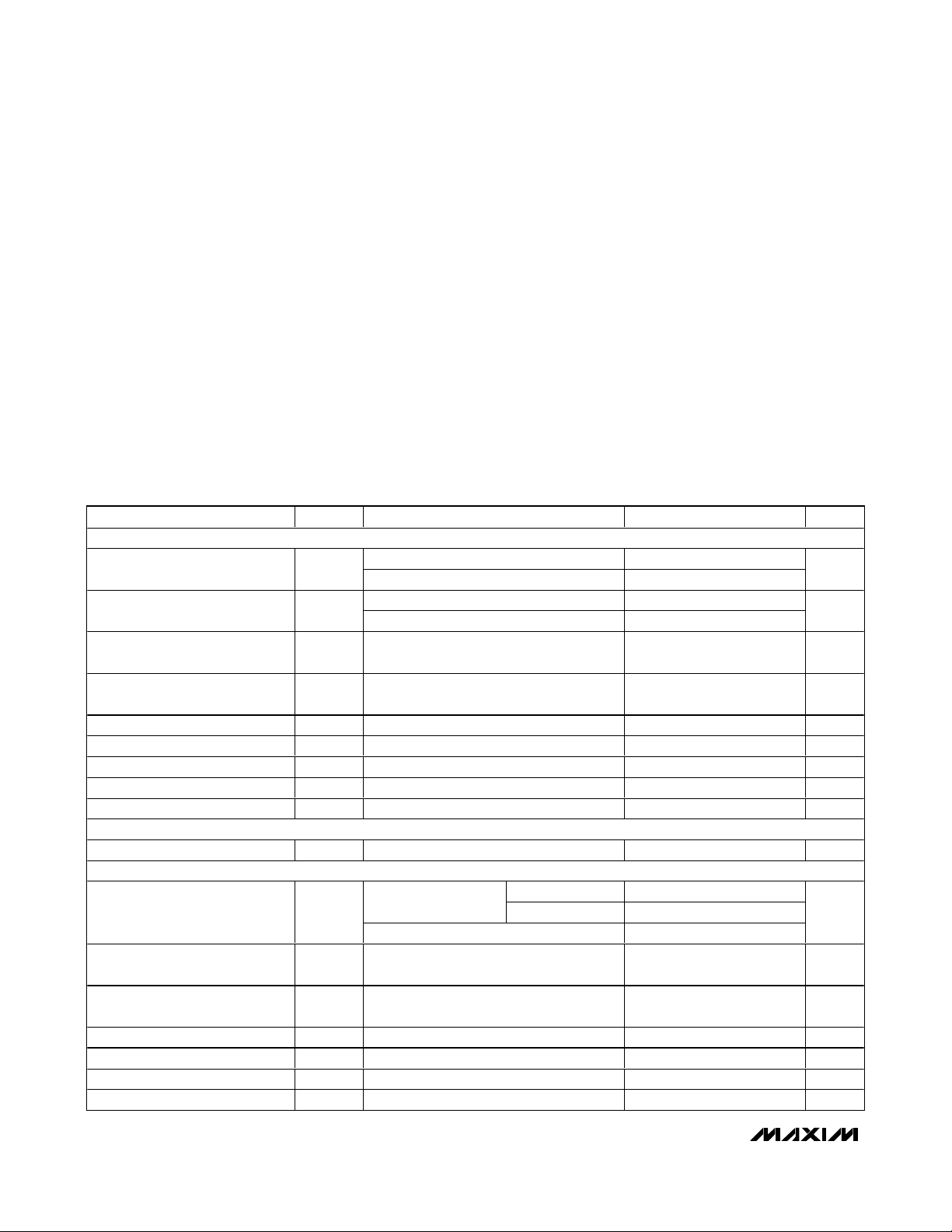
The MAX1493/MAX1495 come in a 32-pin 7mm ✕ 7mm
TQFP package, and the MAX1491 comes in 28-pin
SSOP and 28-pin DIP packages. All devices in this family operate over the 0°C to +70°C commercial temperature range.
Applications
Digital Panel Meters
Hand-Held Meters
Digital Voltmeters
Digital Multimeters
Features
♦ High Resolution
MAX1495: 4.5 Digits (±19,999 Count)
MAX1493: 4.5 Digits (±19,999 Count)
MAX1491: 3.5 Digits (±1999 Count)
♦ Sigma-Delta ADC Architecture
No Integrating Capacitors Required
No Autozeroing Capacitors Required
>100dB of Simultaneous 50Hz and 60Hz Rejection
♦ Operate from a Single 2.7V or 5.25V Supply
♦ Selectable Input Range of ±200mV or ±2V
♦ Selectable Voltage Reference: Internal 2.048V or
External
♦ Internal High-Accuracy Oscillator Needs No
External Components
♦ Automatic Offset Calibration
♦ Low Power: Maximum 980µA Operating Current
♦ Small 32-Pin 7mm
✕ 7mm TQFP Package (4.5
Digits), 28-Pin SSOP Package (3.5 Digits), and 28Pin DIP Package (3.5 Digits)
♦ Triplexed LCD Driver
♦ Evaluation Kit Available (Order MAX1494EVKIT)
MAX1491/MAX1493/MAX1495
3.5- and 4.5-Digit, Single-Chip
ADCs with LCD Drivers
________________________________________________________________ Maxim Integrated Products 1
Pin Configurations
Ordering Information
19-3053; Rev 2; 5/04
For pricing, delivery, and ordering information, please contact Maxim/Dallas Direct! at
1-888-629-4642, or visit Maxim’s website at www.maxim-ic.com.
Pin Configurations continued at end of data sheet.
EVALUATION KIT
AVAILABLE
PART
MAX1491CAI 0°C to +70°C 28 SSOP 3.5
MAX1491CNI 0°C to +70°C 28 DIP 3.5
MAX1493CCJ 0°C to +70°C 32 TQFP 4.5
MAX1495CCJ 0°C to +70°C 32 TQFP 4.5
TEMP
RANGE
PINPACKAGE
RESOLUTION
(DIGITS)
TOP VIEW
AIN+
AIN-
REF-
REF+
LOWBATT
RANGE
DVDDINTREF
GND
32 28
1AV
DD
2
3
4
5
6
7
8DPSET1
10
9
PEAK
DPSET2
NEG
V
293031
MAX1493
MAX1495
SEG1
HOLD
TQFP
13
DPON
SEG2
27
14
BP1
SEG3
26
15
BP2
SEG4
25
1611 12
BP3
SEG5
24 SEG13
SEG12
23
SEG11
22
SEG10
21
SEG9
20
SEG8
19
SEG7
18
SEG6
17
Page 2
MAX1491/MAX1493/MAX1495
3.5- and 4.5-Digit, Single-Chip
ADCs with LCD Drivers
2 _______________________________________________________________________________________
ABSOLUTE MAXIMUM RATINGS
ELECTRICAL CHARACTERISTICS
(AVDD= DVDD= +2.7V to +5.25V, GND = 0, V
REF+
- V
REF-
= 2.048V (external reference), C
NEG
= 0.1µF. All specifications are T
MIN
to T
MAX
, unless otherwise noted. Typical values are at +25°C, unless otherwise noted.)
Stresses beyond those listed under “Absolute Maximum Ratings” may cause permanent damage to the device. These are stress ratings only, and functional
operation of the device at these or any other conditions beyond those indicated in the operational sections of the specifications is not implied. Exposure to
absolute maximum rating conditions for extended periods may affect device reliability.
AVDDto GND............................................................-0.3V to +6V
DV
DD
to GND ...........................................................-0.3V to +6V
AIN+, AIN- to GND...............................V
NEG
to + (AVDD+ 0.3V)
REF+, REF- to GND..............................V
NEG
to + (AVDD+ 0.3V)
LOWBATT to GND ...................................-0.3V to (AV
DD
+ 0.3V)
INTREF, RANGE, DPSET1, DPSET2, PEAK,
HOLD to GND......................................-0.3V to (DV
DD
+ 0.3V)
DPON to GND..........................................-0.3V to (DV
DD
+ 0.3V)
V
NEG
to GND ...........................................-2.6V to (AVDD+ 0.3V)
Maximum Current into Any Pin ...........................................50mA
Continuous Power Dissipation (T
A
= +70°C)
32-Pin TQFP (derate 20.7mW/°C above +70°C).....1652.9mW
28-Pin SSOP (derate 9.5mW/°C above +70°C) ...........762mW
28-Pin DIP (derate 14.3mW/°C above +70°C)........1142.9mW
Operating Temperature Range...............................0°C to +70°C
Junction Temperature......................................................+150°C
Storage Temperature Range .............................-60°C to +150°C
Lead Temperature (soldering, 10s) .................................+300°C
PARAMETER SYMBOL CONDITIONS MIN TYP MAX UNITS
DC ACCURACY
Noise-Free Resolution
Integral Nonlinearity (Note 1) INL
Range Change Accuracy
Rollover Error
Output Noise 10 µV
Offset Error (Zero Input Reading) Offset VIN = 0 (Note 2) -0 +0 Reading
Gain Error (Note 3) -0.5 +0.5 %FSR
Offset Drift (Zero Reading Drift) VIN = 0 0.1 µV/°C
Gain Drift ±1 ppm/°C
INPUT CONVERSION RATE
Conversion Rate 5Hz
ANALOG INPUTS (AIN+, AIN-) (bypass to GND with 0.1µF or greater capacitors)
Normal Mode 50Hz and 60Hz
Rejection (Simultaneously)
Common-Mode 50Hz and 60Hz
Rejection (Simultaneously)
Common-Mode Rejection CMR At DC 100 dB
Input Leakage Current TA = +25°C10nA
Input Capacitance 10 pF
Dynamic Input Current (Note 5) -20 +20 nA
CMR
MAX1493/MAX1495 -19,999 +19,999
MAX1491 -1999 +1999
2.000V range ±1
200mV range ±1
(V
AIN+
(V
AIN+
V
AIN+
V
AIN-
Differential (Note 4)
Absolute GND referenced -2.2V +2.2V
50Hz and 60Hz ±2% 100 dB
For 50Hz ±2% and 60Hz ±2%,
R
SOURCE
- V
= 0.100V) on 200mV range /
AIN-
- V
= 0.100V) on 2.0V range
AIN-
- V
= full scale,
AIN-
- V
= full scale
AIN+
RANGE = GND -2.0 +2.0
RANGE = DV
< 10kΩ
DD
10:1 Ratio
±1.0 Count
-0.2 +0.2AIN Input Voltage Range
150 dB
Count
Count
P-P
V
Page 3
MAX1491/MAX1493/MAX1495
3.5- and 4.5-Digit, Single-Chip
ADCs with LCD Drivers
_______________________________________________________________________________________ 3
ELECTRICAL CHARACTERISTICS (continued)
(AVDD= DVDD= +2.7V to +5.25V, GND = 0, V
REF+
- V
REF-
= 2.048V (external reference), C
NEG
= 0.1µF. All specifications are T
MIN
to T
MAX
, unless otherwise noted. Typical values are at +25°C, unless otherwise noted.)
PARAMETER SYMBOL CONDITIONS MIN TYP MAX UNITS
LOW-BATTERY VOLTAGE MONITOR (LOWBATT)
LOWBATT Trip Threshold 2.048 V
LOWBATT Leakage Current 10 pA
Hysteresis 20 mV
INTERNAL REFERENCE (REF- = GND, INTREF = DVDD, bypass REF+ to GND with 4.7µF capacitors)
REF Output Voltage V
REF Output Short-Circuit Current TA = +25°C1mA
REF Output Temperature
Coefficient
Load Regulation
Line Regulation 50 µV/V
Noise Voltage
EXTERNAL REFERENCE (INTREF = GND, bypass REF+ and REF- to GND with 0.1µF or greater capacitors)
REF Input Voltage
Normal-Mode 50Hz and 60Hz
Rejection (Simultaneously)
Common-Mode 50Hz and 60Hz
Rejection (Simultaneously)
Common-Mode Rejection CMR At DC 100 dB
Input Leakage Current TA = +25°C10nA
Input Capacitance 10 pF
Dynamic Input Current (Note 5) -20 +20 nA
CHARGE PUMP
Output Voltage V
DIGITAL INPUTS (INTREF, RANGE, PEAK, HOLD, DPSET1, DPSET2, DPON)
Input Current I
Input Low Voltage V
Input High Voltage V
Input Hysteresis V
TC
CMR
REF
VREF
NEG
IN
INL
INH
HYS
AVDD = 5V, TA = +25°C 2.007 2.048 2.089 V
AVDD = 5V 40 ppm/°C
I
SOURCE
I
SINK
0.1Hz to 10Hz 25
10Hz to 10kHz 400
Differential (V
Absolute GND referenced -2.2 +2.2
50Hz and 60Hz ±2% 100 dB
For 50Hz ±2% and 60Hz ±2%,
R
SOURCE
VIN = 0 or DV
DVDD = 3.0V 200 mV
= 0µA to 300µA,
= 0µA to 30µA, TA = +25°C (Note 6)
- V
REF+
< 10kΩ
DD
) 2.048
REF-
6 mV/µA
150 dB
-2.6 -2.42 -2.3 V
-10 +10 µA
0.3 x
DV
DD
0.7 x
DV
DD
µVp-p
V
V
V
Page 4
MAX1491/MAX1493/MAX1495
3.5- and 4.5-Digit, Single-Chip
ADCs with LCD Drivers
4 _______________________________________________________________________________________
ELECTRICAL CHARACTERISTICS (continued)
(AVDD= DVDD= +2.7V to +5.25V, GND = 0, V
REF+
- V
REF-
= 2.048V (external reference), C
NEG
= 0.1µF. All specifications are T
MIN
to T
MAX
, unless otherwise noted. Typical values are at +25°C, unless otherwise noted.)
Note 1: Integral nonlinearity is the derivation of the analog values at any code from its theoretical value after nulling the gain error
and offset error.
Note 2: Offset calibrated.
Note 3: Offset nulled.
Note 4: The input voltage range for the analog inputs is given with respect to the voltage on the negative input of the differential pair.
Note 5: For the range of V
AIN+
or V
AIN-
= -2.2V to +2.2V and V
REF+
or V
REF-
= -2.2V to +2.2V.
Note 6: External load must be constant during conversion for specified accuracy. Guaranteed specification of 2mV/mA is a result of
production test limitations.
Note 7: Measured at DC by changing the power-supply voltage from 2.7V to 5.25V and measuring its effect on the conversion error.
PSRR at 50Hz and 60Hz exceeds 120dB with filter notches of 10, 20, 30, 40, 50, or 60Hz.
Note 8: Analog power-supply currents are measured with all digital inputs at either GND or DV
DD
. Digital power-supply currents
measured with all digital inputs at either GND or DV
DD
.
PARAMETER SYMBOL CONDITIONS MIN TYP MAX UNITS
POWER SUPPLY
AVDD Voltage AV
DVDD Voltage DV
Power-Supply Rejection AV
Power-Supply Rejection DV
AVDD Current I
DVDD Current I
LCD DRIVER
RMS Segment-On Voltage
RMS Segment-Off Voltage
Display Multiplex Rate 107 Hz
LCD Data-Update Rate 2.5 Hz
DD
DD
DD
DD
PSRRA(Note 7) 80 dB
PSRRD(Note 7) 100 dB
AVDD
DVDD
(Note 8) 660 µA
DVDD = 5V 320
DVDD = 3.3V 180
2.70 5.25 V
2.70 5.25 V
1.92 x
DV
DD
1 / 3 x
DV
DD
µA
V
V
Page 5
MAX1491/MAX1493/MAX1495
3.5- and 4.5-Digit, Single-Chip
ADCs with LCD Drivers
_______________________________________________________________________________________ 5
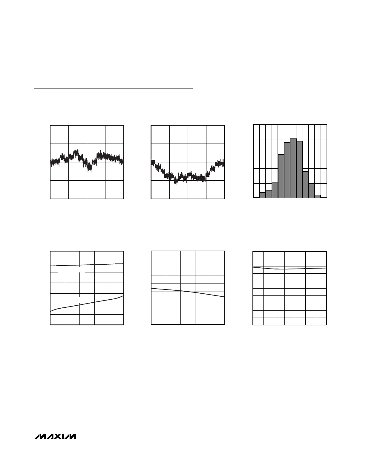
Typical Operating Characteristics
(AVDD= DVDD= 5V, GND = 0, REF+ = 2.048V, REF- = GND, RANGE = DVDD, TA= +25°C.)
MAX1493/MAX1495 (±200mV INPUT RANGE)
INL vs. DISPLAY COUNT
1.0
0.5
0
INL (COUNTS)
-0.5
-1.0
-20,000 20,000
DISPLAY COUNT
10,0000-10,000
SUPPLY CURRENT
vs. SUPPLY VOLTAGE
700
600
ANALOG SUPPLY
500
400
300
SUPPLY CURRENT (µA)
DIGITAL SUPPLY
200
100
0
2.75 5.25
SUPPLY VOLTAGE (V)
4.754.253.753.25
MAX1491/3/5 toc01
MAX1491/3/5 toc04
MAX1493/MAX1495 (±2V INPUT RANGE)
INL vs. DISPLAY COUNT
1.0
0.5
0
INL (COUNTS)
-0.5
-1.0
-20,000 20,000
DISPLAY COUNT
10,0000-10,000
MAX1493/MAX1495
GAIN ERROR vs. SUPPLY VOLTAGE
0.08
0.06
0.04
0.02
0
-0.02
-0.04
GAIN ERROR (% FULL SCALE)
-0.06
-0.08
-0.10
2.75 5.25
SUPPLY VOLTAGE (V)
4.754.253.25 3.75
MAX1491/3/5 toc02
MAX1491/3/5 toc05
25
20
15
10
PERCENTAGE OF UNITS (%)
5
0
0
-0.01
-0.02
-0.03
-0.04
-0.05
-0.06
-0.07
GAIN ERROR (% FULL SCALE)
-0.08
-0.09
-0.10
070
NOISE DISTRIBUTION
-0.2
NOISE (COUNTS)
MAX1493/MAX1495
GAIN ERROR vs. TEMPERATURE
TEMPERATURE (°C)
MAX1491/3/5 toc03
0.80.70.60.50.40.30.20.10-0.1
MAX1491/3/5 toc06
605030 402010
Page 6
MAX1491/MAX1493/MAX1495
3.5- and 4.5-Digit, Single-Chip
ADCs with LCD Drivers
6 _______________________________________________________________________________________
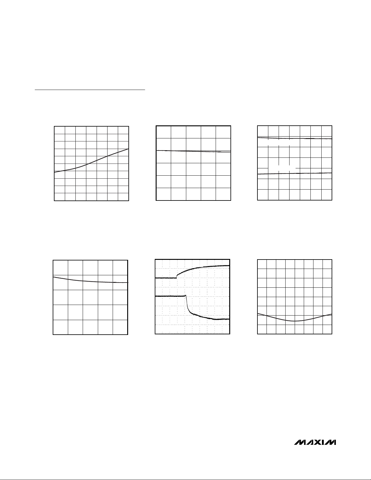
Typical Operating Characteristics (continued)
(AVDD= DVDD= 5V, GND = 0, REF+ = 2.048V, REF- = GND, RANGE = DVDD, TA= +25°C.)
INTERNAL REFERENCE VOLTAGE
vs. TEMPERATURE
2.054
2.053
2.052
2.051
2.050
2.049
2.048
2.047
REFERENCE VOLTAGE (V)
2.046
2.045
2.044
070
TEMPERATURE (°C)
605040302010
2.050
2.049
MAX1491/3/5 toc07
2.048
2.047
2.046
REFERENCE VOLTAGE (V)
2.045
2.044
INTERNAL REFERENCE VOLTAGE
vs. ANALOG SUPPLY VOLTAGE
2.75 5.25
SUPPLY VOLTAGE (V)
CHARGE-PUMP OUTPUT VOLTAGE
V
vs. ANALOG SUPPLY VOLTAGE
-2.40
-2.42
-2.44
VOLTAGE (V)
-2.46
NEG
V
-2.48
-2.50
2.75 5.25
SUPPLY VOLTAGE (V)
MAX1491/3/5 toc10
2V/div
1V/div
4.754.253.753.25
STARTUP SCOPE SHOT
NEG
V
DD
V
NEG
C
= 0.1µF
NEG
20ms/div
SUPPLY CURRENT
vs. TEMPERATURE
700
600
MAX1491/3/5 toc08
SUPPLY CURRENT (µA)
4.754.253.753.25
ANALOG SUPPLY
500
400
300
200
100
DIGITAL SUPPLY
0
070
TEMPERATURE (°C)
MAX1491/3/5 toc09
605040302010
OFFSET ERROR
vs. COMMON-MODE VOLTAGE
0.20
0.15
MAX1491/3/5 toc11
0.10
0.05
0
-0.05
OFFSET ERROR (COUNTS)
-0.10
-0.15
-0.20
-2.0 2.0
COMMON-MODE VOLTAGE (V)
MAX1491/3/5 toc12
1.51.0-1.5 -1.0 -0.5 0 0.5
Page 7
MAX1491/MAX1493/MAX1495
3.5- and 4.5-Digit, Single-Chip
ADCs with LCD Drivers
_______________________________________________________________________________________ 7
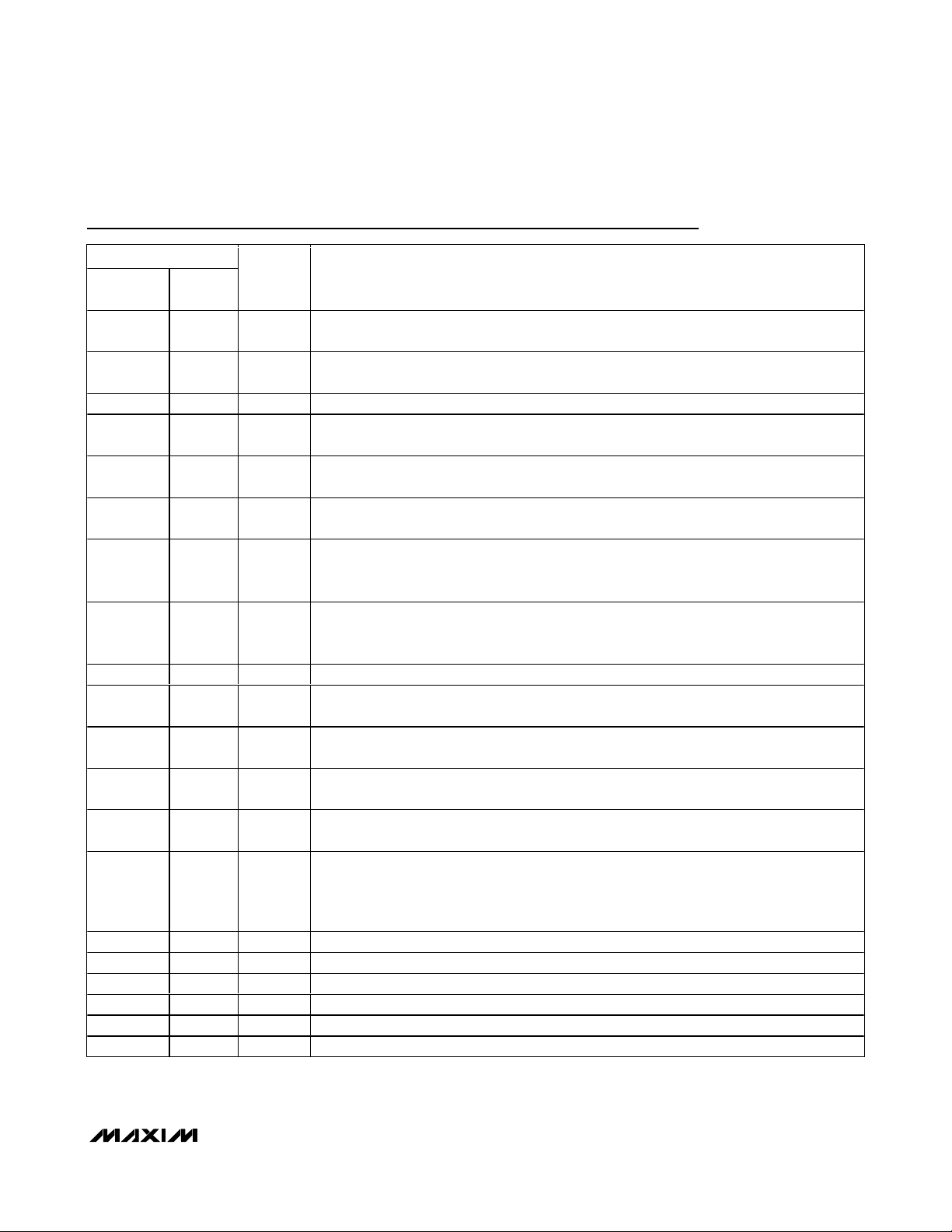
Pin Description
PIN
MAX1491
1 30 INTREF
231DV
3 32 GND Ground
41AV
5 2 AIN+
6 3 AIN-
7 4 REF-
8 5 REF+
9 6 LOWBATT Low Batter y Inp ut. W hen V
10 7 RANGE
11 8 DPSET1
12 9 DPSET2
13 10 PEAK
MAX1493
MAX1495
NAME FUNCTION
Internal Reference Logic Input. Connect to GND to select external reference mode. Connect
to DV
Digital Power Input. Connect DVDD to a 2.7V to 5.25V power supply. Bypass DVDD to GND
DD
with a 0.1µF and a 4.7µF capacitor.
Analog Power Input. Connect AVDD to a 2.7V to 5.25V power supply. Bypass AVDD to GND
DD
with a 0.1µF and a 4.7µF capacitor.
Positive Analog Input. Positive side of fully differential analog input. Bypass A
a 0.1µF or greater capacitor.
Negative Analog Input. Negative side of fully differential analog input. Bypass A
with a 0.1µF or greater capacitor.
Negative Reference Input. For internal reference operation, connect REF- to GND. For
external reference operation, bypass REF- to GND with a 0.1µF capacitor and set V
-2.2V to +2.2V, provided V
Positive Reference Input. For internal reference operation, connect a 4.7µF capacitor from
REF+ to GND. For external reference operation, bypass REF+ to GND with a 0.1µF capacitor
and set V
Range Logic Input. RANGE controls the fully differential analog input range. Connect to GND
for the ±2V input range. Connect to DV
Decimal Point Logic Input 1. Controls the decimal point of the LCD. See the Decimal Point
Control section.
Decimal Point Logic Input 2. Controls the decimal point of the LCD. See the Decimal Point
Control section.
Peak Logic Input. Connect to DV
GND to disable the peak function.
to select the internal reference mode.
DD
from -2.2V to +2.2V, provided V
REF+
> V
REF+
LOWB ATT
to GND with
IN+
to GND
IN-
.
REF-
> V
REF+
< 2.048V ( typ ) , the LO WBATT sym b ol on the LC D tur ns on.
for the ±200mV input range.
DD
to display the highest ADC value on the LCD. Connect to
DD
REF-
.
REF-
from
Hold Logic Input. Connect to DV
14 11 HOLD
15 12 SEG1 LCD Segment 1 Driver
16 13 SEG2 LCD Segment 2 Driver
17 14 SEG3 LCD Segment 3 Driver
18 15 SEG4 LCD Segment 4 Driver
19 16 SEG5 LCD Segment 5 Driver
20 17 SEG6 LCD Segment 6 Driver
GND to update the LCD at a rate of 2.5Hz and disable the hold function. For the MAX1495,
placing the device into hold mode initiates an enhanced offset calibration. Assert HOLD high
for a minimum of 2s to ensure the completion of enhanced offset calibration.
to hold the current ADC value on the LCD. Connect to
DD
Page 8
MAX1491/MAX1493/MAX1495
3.5- and 4.5-Digit, Single-Chip
ADCs with LCD Drivers
8 _______________________________________________________________________________________
Pin Description (continued)
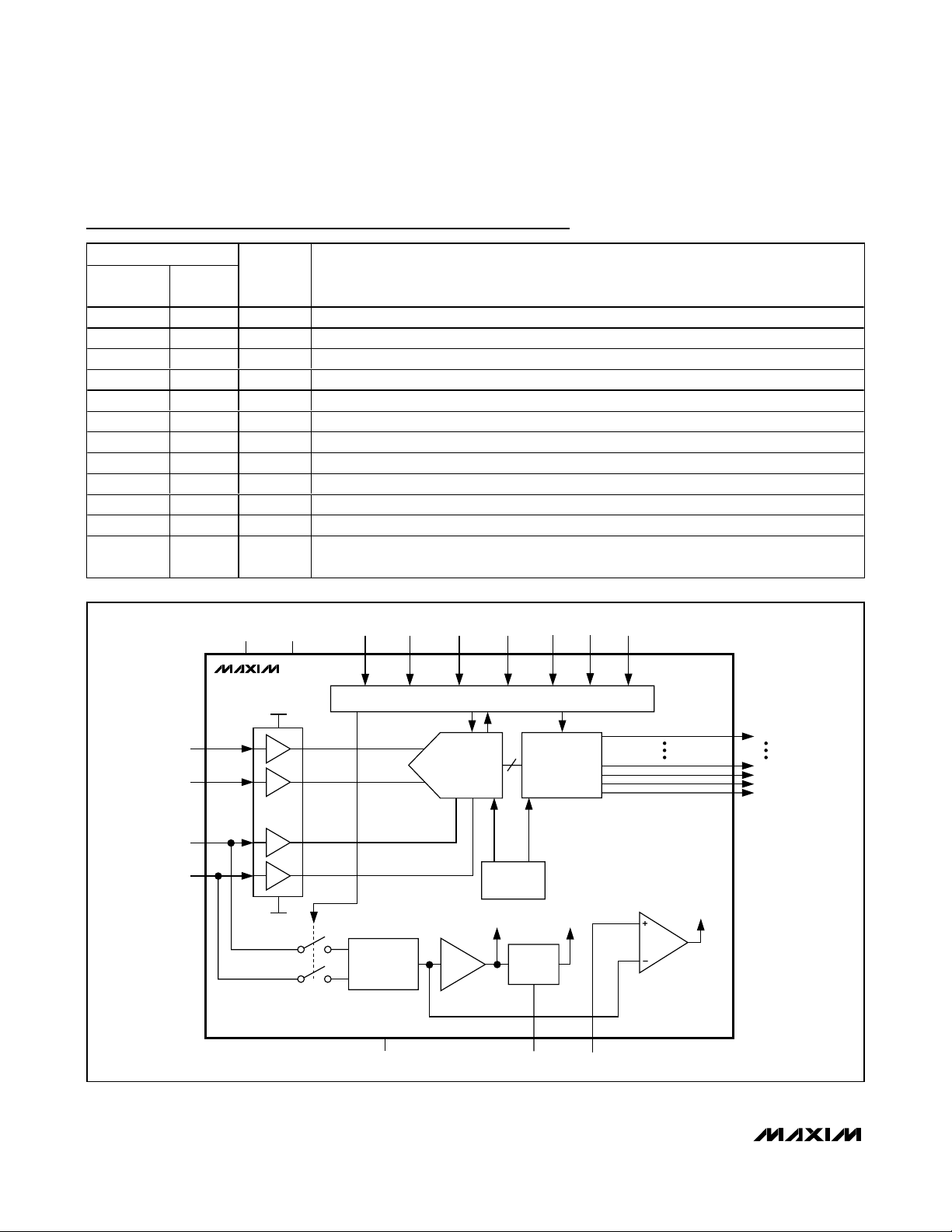
Figure 1. MAX1493/MAX1495 Functional Diagram
PIN
MAX1491
MAX1493
MAX1495
21 18 SEG7 LCD Segment 7 Driver
22 19 SEG8 LCD Segment 8 Driver
23 20 SEG9 LCD Segment 9 Driver
24 21 SEG10 LCD Segment 10 Driver
25 25 BP3 LCD Backplane 3 Driver
26 26 BP2 LCD Backplane 2 Driver
27 27 BP1 LCD Backplane 1 Driver
28 29 V
— 22 SEG11 LCD Segment 11 Driver
— 23 SEG12 LCD Segment 12 Driver
— 24 SEG13 LCD Segment 13 Driver
— 28 DPON
NAME FUNCTION
NEG
-2.5V Charge-Pump Voltage Output. Connect a 0.1µF capacitor from V
Decimal Point Enable Input. Controls the decimal point of the LCD. See the Decimal Point
Control section. Connect to DV
to enable the decimal point.
DD
to GND.
NEG
DV
AV
DD
DD
MAX1493
AIN+
AIN-
REF+
REF-
MAX1495
+2.5V
INPUT
BUFFERS
-2.5V
DPON HOLD
2.048V
BANDGAP
REFERENCE
GND
DPSET1 DPSET2
CONTROL
ADC
OSCILLATOR/
CLOCK
+2.5V
A = 1.22
CHARGE
PUMP
PEAK
RANGE
BINARY-TO-BCD
CONVERTERS
AND
LCD DRIVERS
-2.5V
LOWBATTV
NEG
INTREF
TO
CONTROL
SEG1
SEG13
BP1
BP2
BP3
Page 9

MAX1491/MAX1493/MAX1495
3.5- and 4.5-Digit, Single-Chip
ADCs with LCD Drivers
_______________________________________________________________________________________ 9
Detailed Description
The MAX1491/MAX1493/MAX1495 low-power, highly
integrated ADCs with LCD drivers convert a ±2V differential input voltage (one count is equal to 100µV for the
MAX1493/MAX1495 and 1mV for the MAX1491) with a
sigma-delta ADC and output the result to an LCD. An
additional ±200mV input range (one count is equal to
10µV for the MAX1493/MAX1495 and 100µV for the
MAX1491) is available to measure small signals with
increased resolution.
These devices operate from a single 2.7V to 5.25V power
supply and offer 3.5-digit (MAX1491) or 4.5-digit
(MAX1493/MAX1495) conversion results. An internal
2.048V reference, internal charge pump and a high-accuracy on-chip oscillator eliminate external components.
These devices also feature on-chip buffers for the differential input signal and external reference inputs,
allowing direct interface with high-impedance signal
sources. In addition, they use continuous internal offset
calibration, and offer >100dB of 50Hz and 60Hz line
noise rejection. Other features include data hold and
peak hold, and a low-battery monitor. The MAX1495
also performs enhanced offset calibration on demand.
Analog Input Protection
Internal protection diodes limit the analog input range
from V
NEG
to (AVDD+ 0.3V). If the analog input
exceeds this range, limit the input current to 10mA.
Internal Analog Input/
Reference Buffers
The MAX1491/MAX1493/MAX1495 analog input/reference buffers allow the use of high-impedance signal
sources. The input buffers’ common-mode input range
allows the analog inputs and reference to range from
-2.2V to +2.2V.
Modulator
The MAX1491/MAX1493/MAX1495 perform analog-todigital conversions using a single-bit, 3rd-order, sigmadelta modulator. The sigma-delta modulation converts
the input signal into a digital pulse train whose average
duty cycle represents the digitized signal information.
The modulator quantizes the input signal at a much
higher sample rate than the bandwidth of the input.
The MAX1491/MAX1493/MAX1495 modulator provides
3rd-order frequency shaping of the quantization noise
resulting from the single-bit quantizer. The modulator is
fully differential for maximum signal-to-noise ratio and
minimum susceptibility to power-supply noise. A singlebit data stream is then presented to the digital filter for
processing, to remove the frequency-shaped quantization noise.
Digital Filtering
The MAX1491/MAX1493/MAX1495 contain an on-chip
digital lowpass filter that processes the data stream
from the modulator using a SINC4 (sinx/x)
4
response.
The SINC4filter has a settling time of four output data
periods (4 x 200ms).
The MAX1491/MAX1493/MAX1495 have 25% overrange
capability built into the modulator and digital filter:
Filter Characteristics
Figure 2 shows the filter frequency response. The SINC
4
characteristic -3dB cutoff frequency is 0.228 times the
first notch frequency (5Hz). The oversampling ratio
(OSR) for the MAX1491 is 128 and the OSR for the
MAX1493/MAX1495 is 1024.
The output data rate for the digital filter corresponds
with the positioning of the first notch of the filter’s frequency response. The notches of the SINC
4
filter are
repeated at multiples of the first notch frequency. The
SINC
4
filter provides an attenuation of better than
100dB at these notches. For example, 50Hz is equal to
10 times the first notch frequency and 60Hz is equal to
12 times the first notch frequency.
Hz
N
z
z
()=
()
()
⎡
⎣
⎢
⎢
⎢
⎤
⎦
⎥
⎥
⎥
1
1
1
1
4
-
-
-N
-
Hf
N
N
f
f
f
f
m
m
()
sin
sin
=
⎛
⎝
⎜
⎞
⎠
⎟
⎛
⎝
⎜
⎞
⎠
⎟
⎡
⎣
⎢
⎢
⎢
⎢
⎢
⎤
⎦
⎥
⎥
⎥
⎥
⎥
1
4
π
π
Figure 2. Frequency Response of the SINC4Filter (Notch at 60Hz)
0
-40
-80
GAIN (dB)
-120
-160
-200
060
FREQUENCY (Hz)
5040302010
Page 10

MAX1491/MAX1493/MAX1495
Internal Clock
The MAX1491/MAX1493/MAX1495 contain an internal
oscillator. Using the internal oscillator saves board
space by removing the need for an external clock
source. The oscillator is optimized to give 50Hz and
60Hz power supply and common-mode rejection.
Charge Pump
The MAX1491/MAX1493/MAX1495 contain an internal
charge pump to provide the negative supply voltage for
the internal analog input/reference buffers. The bipolar
input range of the analog input/reference buffers allows
the devices to accept negative inputs with high source
impedances. For the charge pump to operate correctly,
connect a 0.1µF capacitor from V
NEG
to GND.
LCD Driver
The MAX1491/MAX1493/MAX1495 contain the necessary backplane and segment driver outputs to drive
3.5-digit (MAX1491) and 4.5-digit (MAX1493/MAX1495)
LCDs. The LCD update rate is 2.5Hz. Figures 4–7 show
the connection schemes for a standard LCD. The
MAX1491/MAX1493/MAX1495 automatically display the
results of the ADC.
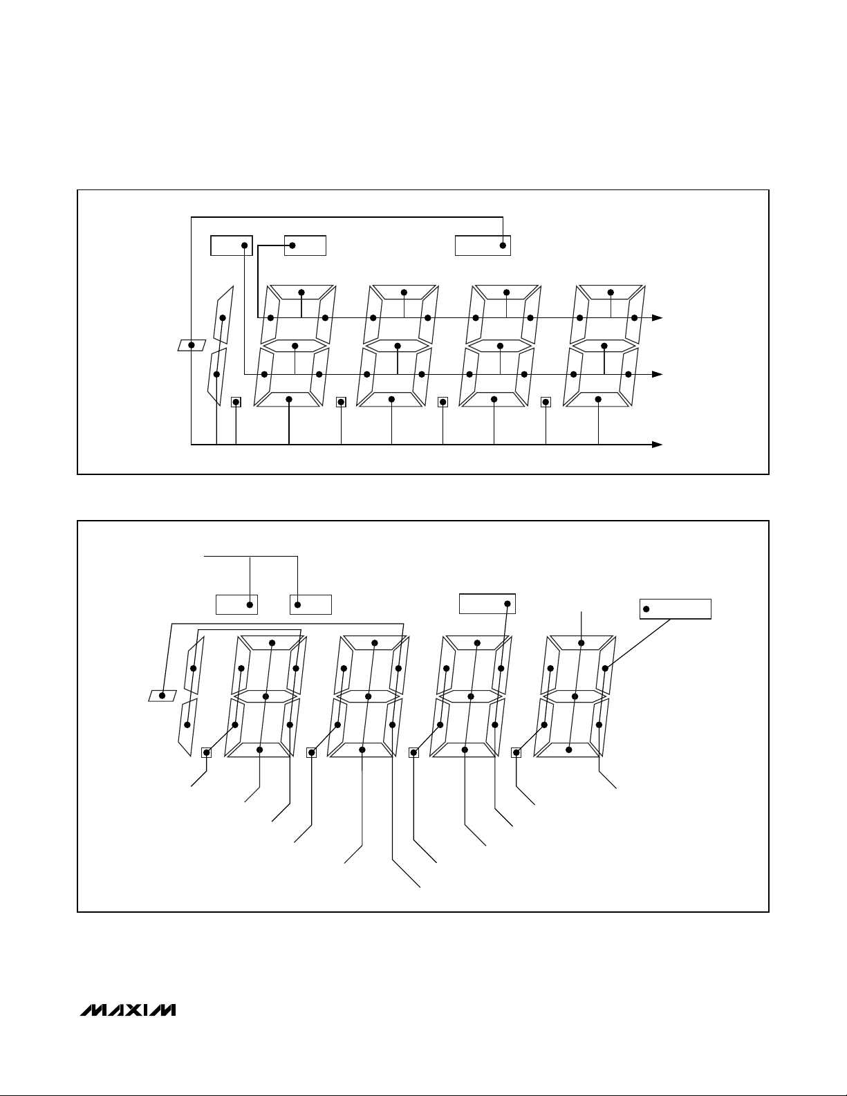
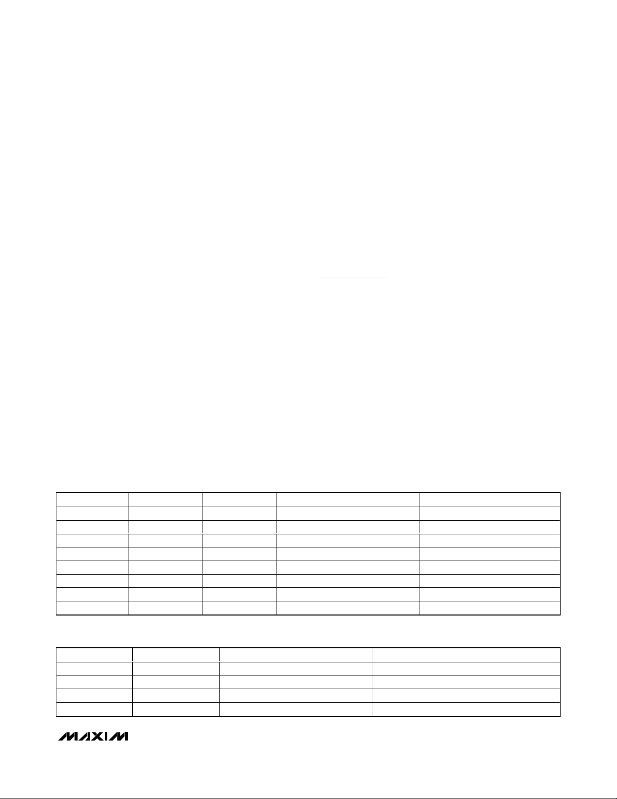
Triplexing
An internal resistor string of three equal-value resistors
(52kΩ, 1% matching) is used to generate the display
drive voltages. One end of the string is connected to
DVDDand the other end is connected to GND. Note that
V
LCD(VLCD
= DVDD- GND) should be three times the
threshold voltage for the liquid-crystal material used.
The connection diagram for a typical 7-segment display
font with two annunciators is illustrated in Figure 3 and
Figure 8. The MAX1491/MAX1493/MAX1495 numeric
display drivers (4.5 digits, 3.5 digits) use this configuration to drive a triplexed LCD with three backplanes and
13 segment driver lines (10 for 3.5 digits). Figures 4 and
5 show the assignment of the 4.5-digit display segments
and Figures 6 and 7 show the assignment of the 3.5digit display segments.
The voltage waveforms of the backplane lines and y
segment line (Figure 3) have been chosen as an example. This line intersects with BP1 to form the a segment,
with BP2 to form the g segment, and with BP3 to form
the d segment. Eight different ON/OFF combinations of
the a, g, and d segments and their corresponding
waveforms of the y segment line are illustrated in
Figures 9 and 10. The schematic diagram in Figure 8
shows that each intersection acts as a capacitance
from segment line to common line. Figure 11 illustrates
the voltage across the g segment.
The RMS voltage across the segment determines the
degree of polarization for the liquid-crystal material and
thus the contrast of the segment. The RMS OFF voltage
is always V
LCD
/ 3, whereas the RMS ON voltage is
always 1.92V
LCD
/ 3. This is illustrated in Figure 11. The
ratio of RMS ON to OFF voltage is fixed at 1.92 for a
triplexed LCD.
Figure 12 illustrates contrast vs. applied RMS voltage
with a V
LCD
of 3.1V. The RMS ON voltage is 2.1V and
the RMS OFF voltage is 1.1V. The OFF segment has a
contrast of less than 5%, while the ON segments have
greater than 85% contrast.
3.5- and 4.5-Digit, Single-Chip
ADCs with LCD Drivers
10 ______________________________________________________________________________________
Table 1. List of LCD Manufacturers
Figure 3. Connection Diagrams for Typical Seven-Segment
Displays
DP
f
Y
a
g
c
d
ANNUNCIATOR
Z
b
BP1
BP2
BP3
f
e
DP ANNUNCIATOR
X
e
a
b
g
c
d
MANUFACTURER WEBSITE PART NUMBER DESCRIPTION
04-0924-00 3.5 digit, 5V
DCI, Inc. www.dciincorporated.com
The following site has links to other custom LCD manufacturers: www.earthlcd.com/mfr.htm
04-0924-01 3.5 digit, 3V
04-0925-00 4.5 digit, 5V
04-0925-01 4.5 digit, 3V
Page 11
MAX1491/MAX1493/MAX1495
3.5- and 4.5-Digit, Single-Chip
ADCs with LCD Drivers
______________________________________________________________________________________ 11
Figure 4. Backplane Connection for the MAX1493/MAX1495 (4.5 Digits)
Figure 5. Segment Connection for the MAX1493/MAX1495 (4.5 Digits)
HOLD LOW BATTPEAK
BP1
BP2
BP3
SEG13: PEAK, HOLD, N.C.
HOLD
SEG12: F4, E4, DP4
SEG11: A4, G4, D4
SEG10: B4, C4, BC5
SEG9: F3, E3, DP3
PEAK
SEG8: A3, G3, D3
SEG7: B3, C3, MINUS
LOW BATT
SEG5: A2, G2, D2
SEG6: F2, E2, DP2
SEG2: A1, G1, D1
SEG3: F1, E1, DP1
SEG4: B2, C2, LOWBATT
ANNUNCIATOR
SEG1: B1, C1, ANNUNCIATOR
Page 12

MAX1491/MAX1493/MAX1495
3.5- and 4.5-Digit, Single-Chip
ADCs with LCD Drivers
12 ______________________________________________________________________________________
Figure 6. Backplane Connection for the MAX1491 (3.5 Digits)
Figure 7. Segment Connection for the MAX1491 (3.5 Digits)
Figure 8. Schematic of Display Digit
HOLD LOW BATTPEAK
SEG10: PEAK, HOLD, BC4
BP1
BP2
BP3
HOLD
PEAK
LOW BATT
SEG9: F3, E3, DP3
SEG8: A3, G3, D3
XYZ
BP1
BP2
f
e
ab
g
c
SEG6: F2, E2, DP2
SEG7: B3, C3, MINUS
SEG5: A2, G2, D2
SEG2: A1, G1, D1
SEG3: F1, E1, DP1
SEG4: B2, C2, LOWBATT
ANNUNCIATOR
SEG1: B1, C1, ANNUNCIATOR
BP3
DP
d
DP
Page 13

MAX1491/MAX1493/MAX1495
3.5- and 4.5-Digit, Single-Chip
ADCs with LCD Drivers
______________________________________________________________________________________ 13
BP1
Figure 9. LCD Voltage Waveform—Combinations 1–4 (BP1/2/3, SEGa/d/g)
BP2
BP3
ALL
OFF
φ1 φ2 φ3 φ1' φ2' φ3'
V+
V
H
V
V
V-
V+
V
V
V-
V+
V
V
V-
V+
V
V
V-
LCD
L
H
L
H
L
H
L
a ON
g, d OFF
g ON
a, d OFF
d ON
a, g OFF
FREQUENCY = 107Hz
φ1, φ2, φ3 - - BP HIGH WITH RESPECT TO SEGMENT (BP+ TIME)
φ1', φ2', φ3' - - BP LOW WITH RESPECT TO SEGMENT (BP- TIME)
BP1 ACTIVE DURING φ1 AND φ1'
BP2 ACTIVE DURING φ2 AND φ2'
BP3 ACTIVE DURING φ3 AND φ3'
V+ = DV
VL = 1/3 V
= DVDD - GND
V
LCD
, VH = 2/3 DV
DD
, V- = GND
LCD
V+
V
H
V
L
V-
V+
V
H
V
L
V-
V+
V
H
V
L
V-
DD
Page 14

MAX1491/MAX1493/MAX1495
3.5- and 4.5-Digit, Single-Chip
ADCs with LCD Drivers
14 ______________________________________________________________________________________
Figure 10. LCD Voltage Waveform—Combinations 5–8 (BP1/2/3, SEGa/d/g)
φ1 φ2 φ3 φ1' φ2' φ3'
BP1
BP2
BP3
ALL
OFF
a, d ON
g OFF
a, g ON
d OFF
g, d ON
a OFF
V+
V
H
V
V
V-
V+
V
V
V-
V+
V
V
V-
V+
V
V
V-
V+
V
V
V-
V+
V
V
V-
V+
V
V
V-
LCD
L
H
L
H
L
H
L
H
L
H
L
H
L
FREQUENCY = 107Hz
φ1, φ2, φ3 - - BP HIGH WITH RESPECT TO SEGMENT (BP+ TIME)
φ1', φ2', φ3' - - BP LOW WITH RESPECT TO SEGMENT (BP- TIME)
BP1 ACTIVE DURING φ1 AND φ1'
BP2 ACTIVE DURING φ2 AND φ2'
BP3 ACTIVE DURING φ3 AND φ3'
V+ = DV
VL = 1/3 V
= DVDD - GND
V
LCD
, VH = 2/3 DV
DD
, V- = GND
LCD
DD
Page 15

MAX1491/MAX1493/MAX1495
3.5- and 4.5-Digit, Single-Chip
ADCs with LCD Drivers
______________________________________________________________________________________ 15
Figure 11. Voltage Waveforms on the g Segment
φ1 φ2 φ3 φ1' φ2' φ3'
V
LCD
a ON
g, d OFF
a, g ON
d OFF
ALL
OFF
= V
RMS
RMS
RMS
LCD
= V
LCD
= 1.92V
/ 3 (OFF)
/ 3 (OFF)
/ 3 (ON)
LCD
V
0
-V
LCD
V
LCD
V
0
-V
LCD
V
LCD
V
0
-V
LCD
V
LCD
ALL
ON
= VY - V
V
G
VOLTAGE CONTRAST RATIO = V
φ1, φ2, φ3 - - BP HIGH WITH RESPECT TO SEGMENT (BP+ TIME)
φ1', φ2', φ3' - - BP LOW WITH RESPECT TO SEGMENT (BP- TIME)
BP1 ACTIVE DURING φ1 AND φ1'
BP2 ACTIVE DURING φ2 AND φ2'
BP3 ACTIVE DURING φ3 AND φ3'
(DIFFERENCE BETWEEN SEGMENT LINE Y AND BP2 VOLTAGE)
BP2
RMS
ON / V
RMSOFF
= 1.922
= 1.92V
V
RMS
0
-V
LCD
LCD
/ 3 (ON)
Page 16

MAX1491/MAX1493/MAX1495
3.5- and 4.5-Digit, Single-Chip
ADCs with LCD Drivers
16 ______________________________________________________________________________________
Figure 12. Contrast vs. Applied RMS Voltage
100
90
Ø = -10°C
80
Ø = 0°C
V
ON
= 2.1V
RMS
Ø = +10°C
RMS
TA = +25°C
)
70
Ø = -30°C
60
50
40
CONTRAST (%)
30
V
=
OFF
20
1.1V
RMS
10
0
012345
APPLIED VOLTAGE (V
Ø+
Ø-
Page 17
MAX1491/MAX1493/MAX1495
3.5- and 4.5-Digit, Single-Chip
ADCs with LCD Drivers
______________________________________________________________________________________ 17
If ghosting is present on the LCD, the RMS OFF voltage
is too high. Choose an LCD with a higher RMS OFF
voltage or decrease DVDD.
Decimal Point Control
The MAX1491/MAX1493/MAX1495 allow for full decimal-point control and feature leading-zero suppression.
Use DPON, DPSET1, and DPSET2 to set the value of
the decimal point. Tables 2 and 3 show the truth tables
of the DPON, DPSET1, and DPSET2 that determine
which decimal point is used.
Reference
The MAX1491/MAX1493/MAX1495 reference sets the
full-scale range of the ADC transfer function. With a
nominal 2.048V reference, the ADC full-scale range is
±2V with RANGE equal to GND. With RANGE equal to
DVDD, the full-scale range is ±200mV. A decreased reference voltage decreases full-scale range (see the
Transfer Functions section).
The MAX1491/MAX1493/MAX1495 accept either an
external reference or an internal reference. The INTREF
input selects the reference mode.
For internal reference operation, connect INTREF to
DVDD, connect REF- to GND, and bypass REF+ to
GND with a 4.7µF capacitor. The internal reference provides a nominal 2.048V source between REF+ and
GND. The internal reference temperature coefficient is
typically 40ppm/°C.
Connect INTREF to GND to use the external reference.
The external reference inputs, REF+ and REF-, are fully
differential. For a valid external reference input, V
REF+
must be greater than V
REF-
. Bypass REF+ and REFwith a 0.1µF or greater capacitor to GND in external reference mode.
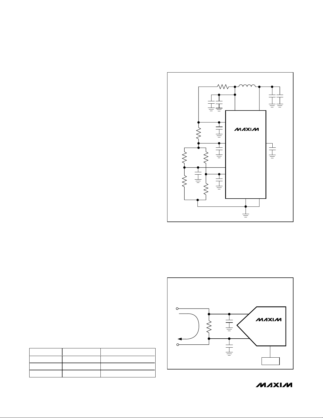
Figure 13 shows the MAX1493/MAX1495 operating with
an external differential reference. In this mode, REF- is
connected to the top of the strain gauge and REF+ is
connected to the midpoint of the resistor-divider on the
supply.
Applications Information
Power-On
At power-on, the digital filter and modulator circuits
reset. The MAX1493/MAX1495 allow 6s for the reference to stabilize before performing enhanced offset
calibration. During these 6s, the MAX1493/MAX1495
display 1.2V to 1.5V when a stable reference is detected. If a valid reference is not found, the MAX1493/
MAX1495 time out after 6s and begin enhanced offset
calibration. Enhanced offset calibration typically lasts
2s. The MAX1493/MAX1495 begin converting after
enhanced offset calibration.
Offset Calibration
The MAX1491/MAX1493/MAX1495 offer on-chip offset
calibration. The MAX1491/MAX1493/MAX1495 calibrate
offset during every conversion cycle. The MAX1495
Table 2. Decimal-Point Control Table (MAX1493/MAX1495)
Table 3. Decimal-Point Control Table (MAX1491)
DPON DPSET1 DPSET2 DISPLAY OUTPUT ZERO INPUT READING
0 0 0 1 8 8 8 8 0
0 0 1 1 8 8 8 8 0
0 1 0 1 8 8 8 8 0
0 1 1 1 8 8 8 8 0
1 0 0 1 8 8 8.8 0.0
1 0 1 1 8 8.8 8 0.00
1 1 0 1 8.8 8 8 0.000
1 1 1 1.8 8 8 8 0.0000
DPSET1 DPSET2 DISPLAY OUTPUT ZERO INPUT READING
0 0 1 8 8.8 0.0
0 1 1 8.8 8 0.00
1 0 1.8 8 8 0.000
1 1 1 8 8 8 000
Page 18
MAX1491/MAX1493/MAX1495
3.5- and 4.5-Digit, Single-Chip
ADCs with LCD Drivers
18 ______________________________________________________________________________________
offers enhanced offset calibration on demand. Connect
HOLD to DVDDfor 2s to perform enhanced offset calibration.
Peak
The MAX1491/MAX1493/MAX1495 feature peak detection circuitry. When activated (PEAK connected to DVDD),
the devices display only the highest voltage measured to
the LCD. First, the current ADC result is displayed. Then
the new ADC conversion result is compared to this value.
If the new value is larger than the previous peak value,
the new value is displayed. If the new value is less than
the previous peak value, the display remains unchanged.
Connect PEAK to GND to clear the peak value and disable the peak function. The peak function is only valid for
the -19,487 to +19,999 range for the MAX1493/
MAX1495 and -1217 to +1999 for the MAX1491.
Hold
The MAX1491/MAX1493/MAX1495 feature data HOLD
circuitry. When activated (HOLD connected to DVDD),
the devices hold the current reading on the LCD.
Low Battery
The MAX1491/MAX1493/MAX1495 feature a low-battery
detection input. When the voltage at LOWBATT drops
below 2.048V (typ), the LOWBATT segment of the LCD
turns on.
Strain Gauge Measurement
Connect the differential inputs of the MAX1491/
MAX1493/MAX1495 to the bridge network of the strain
gauge. In Figure 13, the analog supply voltage powers
the bridge network and the MAX1491/MAX1493/
MAX1495 along with its reference voltage. The
MAX1491/MAX1493/MAX1495 handle an analog input
voltage range of ±200mV or ±2V full scale. The analog/reference inputs of the part allow the analog input
range to have an absolute value anywhere between
-2.2V and +2.2V.
4–20mA Measurement
To measure 4–20mA signals, connect a shunt resistor
across AIN+ and AIN- to create the ±2V or ±200mV
input voltage (see Figure 14).
Table 4. LCD Priority Table
Figure 13. Strain-Gauge Application with the MAX1491/MAX1493/
MAX1495
Figure 14. 4–20mA Measurement
ACTIVE
GAUGE
DUMMY
GAUGE
R
0.1µF
ANALOG SUPPLY
FERRITE
BEAD
0.1µF
0.1µF
REF
0.1µF
R
0.1µF
R
4.7µF
REF+
REF-
AIN+
AIN-
AV
DD
MAX1491
MAX1493
MAX1495
GND
R = 100
Ω for ±200mV RANGE
10
0.1µF
DV
DD
V
NEG
INTREF
Ω for ±2V RANGE
4.7µF
0.1µF
4–20mA
HOLD PEAK DISPLAYS
DV
DD
GND DV
GND GND Latest ADC result
X Current value
DD
Peak value
0.1µF
R
0.1µF
AIN+
AIN-
MAX1491
MAX1493
MAX1495
±1.8.8.8.8
Page 19

Transfer Functions
Figures 15–18 show the MAX1491/MAX1493s’ transfer
functions. The transfer function for the MAX1493/
MAX1495 with AIN+ - AIN- ≥ 0 and RANGE = GND is:
The transfer function for the MAX1493 with AIN+ - AIN< 0 and RANGE = GND is:
The transfer function for the MAX1491 with AIN+ - AIN≥ 0 and RANGE = GND is:
The transfer function for the MAX1491 with AIN+ - AIN< 0 and RANGE = GND is:
The transfer function for the MAX1493/MAX1495 with
AIN+ - AIN- ≥ 0 and RANGE = DV
DD
is:
The transfer function for the MAX1493 with AIN+ - AIN< 0 and RANGE = DVDDis:
The transfer function for the MAX1491 with AIN+ - AIN≥ 0 and RANGE = DVDDis:
The transfer function for the MAX1491 with AIN+ - AIN< 0 and RANGE = DVDDis:
Counts
VV
VV
AIN AIN
REF REF
=× ×
⎛
⎝
⎜
⎞
⎠
⎟
×+
+
+
1 024 2000 10 1.
-
-
-
-
Counts
VV
VV
AIN AIN
REF REF
=×
⎛
⎝
⎜
⎞
⎠
⎟
××
+
+
1 024 2000 10.
-
-
-
-
Counts
VV
VV
AIN AIN
REF REF
=× ×
⎛
⎝
⎜
⎞
⎠
⎟
×+
+
+
1 024 20 000 10 1. ,
-
-
-
-
Counts
VV
VV
AIN AIN
REF REF
=×
⎛
⎝
⎜
⎞
⎠
⎟
××
+
+
1 024 20 000 10. ,
-
-
-
-
Counts
VV
VV
AIN AIN
REF REF
=× ×
⎛
⎝
⎜
⎞
⎠
⎟
+
+
+
1 024 2000 1.
-
-
-
-
Counts
VV
VV
AIN AIN
REF REF
=×
⎛
⎝
⎜
⎞
⎠
⎟
×
+
+
1 024 2000.
-
-
-
-
Counts
VV
VV
AIN AIN
REF REF
=× ×
⎛
⎝
⎜
⎞
⎠
⎟
+
+
+
1 024 20 000 1. ,
-
-
-
-
Counts
VV
VV
AIN AIN
REF REF
=×
⎛
⎝
⎜
⎞
⎠
⎟
×
+
+
1 024 20 000. ,
-
-
-
-
MAX1491/MAX1493/MAX1495
3.5- and 4.5-Digit, Single-Chip
ADCs with LCD Drivers
______________________________________________________________________________________ 19
Figure 15. MAX1493/MAX1495 Transfer Function ±2V Range
Figure 16. MAX1493/MAX1495 Transfer Function ±200mV Range
LCD
1 - - - -
19,999
2
1
0
- 0
- 1
- 2
-19,999
- 1 - - - -
100µV
-100µV
-2V
0
ANALOG INPUT VOLTAGE
+2V
LCD
1 - - - -
19,999
2
1
0
- 0
- 1
- 2
-19,999
- 1 - - - -
10µV
-10µV
-200mV
0
ANALOG INPUT VOLTAGE
+200mV
Page 20

MAX1491/MAX1493/MAX1495
Supplies, Layout, and Bypassing
Power up AVDDand DVDDbefore applying an analog
input and external reference voltage to the device. If
this is not possible, limit the current into these inputs to
50mA. Isolate the digital supply from the analog supply
with a low-value resistor (10Ω) or ferrite bead when the
analog and digital supplies come from the same
source. For best performance, ground the MAX1491/
MAX1493/MAX1495 to the analog ground plane of the
circuit board.
Avoid running digital lines under the device, because
these may couple noise onto the die. Run the analog
ground plane under the MAX1491/MAX1493/MAX1495
to minimize coupling of digital noise. Make the powersupply lines to the MAX1491/MAX1493/MAX1495 as
wide as possible to provide low-impedance paths and
reduce the effects of glitches on the power-supply line.
Shield fast-switching signals, such as clocks, with digital
ground to avoid radiating noise to other sections of the
board. Avoid running clock signals near the analog
inputs. Avoid crossover of digital and analog signals.
Running traces that are on opposite sides of the board at
right angles to each other reduces feedthrough effects.
Good decoupling is important when using high-resolution ADCs. Decouple the supplies with 4.7µF and 0.1µF
ceramic capacitors to GND. Place these components
as close to the device as possible to achieve the
best decoupling.
Refer to the MAX1494 evaluation kit manual for the recommended layout. The evaluation board package
includes a fully assembled and tested evaluation board.
Definitions
INL
Integral nonlinearity (INL) is the deviation of the values
on an actual transfer function from a straight line. This
straight line is either a best-straight-line fit or a line
drawn between the end points of the transfer function,
once offset and gain errors have been nullified. INL for
the MAX1491/MAX1493/MAX1495 is measured using
the end-point method.
DNL
Differential nonlinearity (DNL) is the difference between
an actual step width and the ideal value of one count. A
DNL error specification of less than one count guarantees
no missing counts and a monotonic transfer function.
Rollover Error
Rollover error is defined as the absolute value difference between a near-positive full-scale reading and
near-negative full-scale reading. Rollover error is tested
by applying a full-scale positive voltage, swapping
AIN+ and AIN-, and then adding the results.
Zero Input Reading
Ideally, with AIN+ connected to AIN-, the MAX1491/
MAX1493/MAX1495 display a zero. Zero input reading
is the measured deviation from the ideal zero and the
actual measured point.
3.5- and 4.5-Digit, Single-Chip
ADCs with LCD Drivers
20 ______________________________________________________________________________________
Figure 18. MAX1491 Transfer Function ±2V Range
Figure 17. MAX1491 Transfer Function ±200mV Range
LCD
1 - - -
1999
2
1
0
- 0
- 1
- 2
-1999
- 1 - - -
100µV
0
-200mV
-100µV
ANALOG INPUT VOLTAGE
+200mV
LCD
1 - - -
-1999
- 1 - - -
1999
2
1
0
- 0
- 1
- 2
-1mV
0
-2V
ANALOG INPUT VOLTAGE
1mV
+2V
Page 21
MAX1491/MAX1493/MAX1495
3.5- and 4.5-Digit, Single-Chip
ADCs with LCD Drivers
______________________________________________________________________________________ 21
Typical Operating Circuit
Gain Error
Gain error is the amount of deviation between the measured full-scale transition point and the ideal full-scale
transition point.
Common-Mode Rejection
Common-mode rejection is the ability of a device to
reject a signal that is common to both input terminals.
The common-mode signal can be either an AC or a DC
signal or a combination of the two. CMR is often
expressed in decibels.
Normal-Mode 50Hz and 60Hz Rejection
(Simultaneously)
Normal mode rejection is a measure of how much output
changes when 50Hz and 60Hz signals are injected into
just one of the differential inputs. The MAX1491/
MAX1493/MAX1495 sigma-delta converter uses its internal digital filter to provide normal mode rejection to both
50Hz and 60Hz power-line frequencies simultaneously.
Power-Supply Rejection Ratio
Power-supply rejection ratio (PSRR) is the ratio of the
input supply change (in volts) to the change in the converter output (in volts). It is measured typically
in decibels.
Enhanced Offset Calibration
Enhanced offset calibration is a more accurate calibration method that is needed in the case of the ±200mV
range and 4.5-digit resolution. The MAX1493/MAX1495
perform the enhanced offset calibration upon power-up.
The MAX1495 also performs enhanced offset calibration
on demand with the HOLD input.
HOLD PEAK LOW BATTERY
BACKPLANE
CONNECTIONS
INTREF
DPSET1
DPSET2
RANGE
PEAK
HOLD
DPON
DV
DD
R
LOW
SEG1–SEG13
(SEG1–SEG10)
MAX1493
MAX1495
(MAX1491)
NEG
0.1µF 4.7µF
GND REF- REF+
V
IN
0.1µF
4.7µF
L
ISO
2.7V TO
5.25V
0.1µF
0.1µF
4.7µF
10µF
AIN+
AIN-
DV
AV
DD
DD
LOWBATT V
R
HI
Page 22

MAX1491/MAX1493/MAX1495
3.5- and 4.5-Digit, Single-Chip
ADCs with LCD Drivers
22 ______________________________________________________________________________________
Pin Configurations (continued)
Chip Information
TRANSISTOR COUNT: 79,435
PROCESS: BiCMOS
TOP VIEW
INTREF
DV
GND
AV
AIN+
AIN-
REF-
REF+
LOWBATT
RANGE
DPSET1
DPSET2
PEAK
HOLD
1
2
DD
3
4
DD
5
6
7
8
9
10
11
12
13
14
SSOP OR DIP
MAX1491
28
V
NEG
27
BP1
26
BP2
25
BP3
24
SEG10
23
SEG9
22
SEG8
21
SEG7
20
SEG6
19
SEG5
18
SEG4
17
SEG3
16
SEG2
15
SEG1
Page 23

MAX1491/MAX1493/MAX1495
3.5- and 4.5-Digit, Single-Chip
ADCs with LCD Drivers
______________________________________________________________________________________ 23
Package Information
(The package drawing(s) in this data sheet may not reflect the most current specifications. For the latest package outline information
go to www.maxim-ic.com/packages
.)
32L/48L,TQFP.EPS
Page 24

MAX1491/MAX1493/MAX1495
3.5- and 4.5-Digit, Single-Chip
ADCs with LCD Drivers
24 ______________________________________________________________________________________
Package Information (continued)
(The package drawing(s) in this data sheet may not reflect the most current specifications. For the latest package outline information
go to www.maxim-ic.com/packages
.)
12
INCHES
DIM
A
A1
B
HE
N
A
e
D
B
A1
C
D
E
e
H
L
MAX
MIN
0.068
0.078
0.002
0.008
0.010
0.015
0.004
0.008
SEE VARIATIONS
0.205
0.212
0.0256 BSC
0.301
0.311
0.025
0.037
0∞
L
8∞
NOTES:
1. D&E DO NOT INCLUDE MOLD FLASH.
2. MOLD FLASH OR PROTRUSIONS NOT TO EXCEED .15 MM (.006").
3. CONTROLLING DIMENSION: MILLIMETERS.
4. MEETS JEDEC MO150.
5. LEADS TO BE COPLANAR WITHIN 0.10 MM.
MILLIMETERS
MAX
MIN
1.73 1.99
0.21
0.05
0.38
0.25
0.20
0.09
5.38
5.20
0.65 BSC
7.65
7.90
0.63
0.95
0∞
8∞
INCHES
MIN
D
0.239
D
0.239
D
0.278
D
0.317
0.397
D
PROPRIETARY INFORMATION
TITLE:
MAX
0.249
0.249
0.289
0.328
0.407
MILLIMETERS
MAX
MIN
6.07
6.33
6.07
6.33
7.07
7.33
8.07
8.33
10.07
10.33
PACKAGE OUTLINE, SSOP, 5.3 MM
21-0056
SSOP.EPS
N
14L
16L
20L
24L
28L
C
REV.DOCUMENT CONTROL NO.APPROVAL
1
C
1
Page 25

MAX1491/MAX1493/MAX1495
3.5- and 4.5-Digit, Single-Chip
ADCs with LCD Drivers
Maxim cannot assume responsibility for use of any circuitry other than circuitry entirely embodied in a Maxim product. No circuit patent licenses are
implied. Maxim reserves the right to change the circuitry and specifications without notice at any time.
Maxim Integrated Products, 120 San Gabriel Drive, Sunnyvale, CA 94086 408-737-7600 ____________________ 25
© 2004 Maxim Integrated Products Printed USA is a registered trademark of Maxim Integrated Products.
Package Information (continued)
(The package drawing(s) in this data sheet may not reflect the most current specifications. For the latest package outline information
go to www.maxim-ic.com/packages
.)
PDIPN.EPS
 Loading...