

Page 1
19-5916; Rev 0; 8/11
MAX14821
IO-Link Device Transceiver
General Description
The MAX14821 transceiver is suitable for IO-Link®
devices and 24V binary sensors/actuators. All specified
IO-Link data rates are supported. In IO-Link applications, the transceiver acts as the physical layer interface
to a microcontroller running the data-link layer protocol.
Additional 24V digital inputs and outputs are provided.
Two internal linear regulators generate common sensor
and actuator power requirements: 5V and 3.3V.
On-board C/Q and DO drivers are independently configurable for push-pull, high-side (PNP), or low-side (NPN)
operation. The device detects the IO-Link C/Q wake-up
condition and generates a wake-up signal on the activelow WU output. The C/Q and DI inputs have selectable
current loads for use in actuators.
An SPI™ interface allows configuration and monitoring of
the device. Extensive alarm conditions are detected and
communicated through the IRQ output and the SPI interface. The device features reverse-polarity, short-circuit,
and thermal protection. All power lines are monitored for
undervoltage conditions.
The C/Q and DO drivers are specified for sourcing/sinking up to 100mA.
The device is available in a 2.5mm x 2.5mm, 25-pin WLP
and a 4mm x 4mm, 24-pin TQFN package. Both are specified over the extended -40NC to +85NC temperature range.
Applications
IO-Link Sensors Industrial Sensors and Actuators
IO-Link Actuators
Features
S IO-Link Specification v.1.0 and v.1.1 Physical Layer-
Compliant
S Supports COM1, COM2, and COM3 Data Rates
S IO-Link Device Wake-Up Detection
S Push-Pull, High-Side, or Low-Side Outputs
S 100mA Specified C/Q Output Drive
S Auxiliary 24V, 100mA Digital Output
S Auxiliary 24V Digital Input
S Optional 6mA/7mA Current Loads at Both 24V Inputs
S 5V and 3.3V Linear Regulators
S Reverse-Polarity Protected 24V Supply Output
S EMI Emission Control Through Slew-Controlled Driver
S SPI Interface for Configuration and Monitoring
S 2.5V to 5V Logic Interface Levels
S Reverse-Polarity and Short-Circuit Protection on All
24V Inputs/Outputs
S High-Temperature Warning and Thermal Shutdown
S Extensive Fault Monitoring and Reporting
S -40NC to +85NC Operating Temperature Range
S 2.5mm x 2.5mm WLP and 4mm x 4mm TQFN
Packages
Ordering Information appears at end of data sheet.
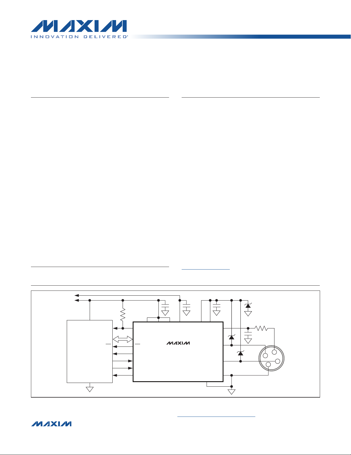
Typical Operating Circuit
5V
3.3V
10kΩ
V
CC
MICROCONTROLLER
GND
IO-Link is a registered trademark of Profibus User Organization (PNO).
SPI is a trademark of Motorola, Inc.
For related parts and recommended products to use with this part, refer to: www.maxim-ic.com/MAX14821.related
����������������������������������������������������������������� Maxim Integrated Products 1
UVGPIO2
SPI
WUIRQ
RXRX
TXCTX
TXENRTS
LOGPIO1
LDO33VLTXQ
MAX14821
V
LDOIN
5
0.1μF1μF 0.1μF
1μF
0.8Ω
L+
1
2
4
3
L-
V
P
V
CC
DO
C/Q
GND
DI
For pricing, delivery, and ordering information, please contact Maxim Direct at 1-888-629-4642,
or visit Maxim’s website at www.maxim-ic.com.
Page 2
MAX14821
IO-Link Device Transceiver
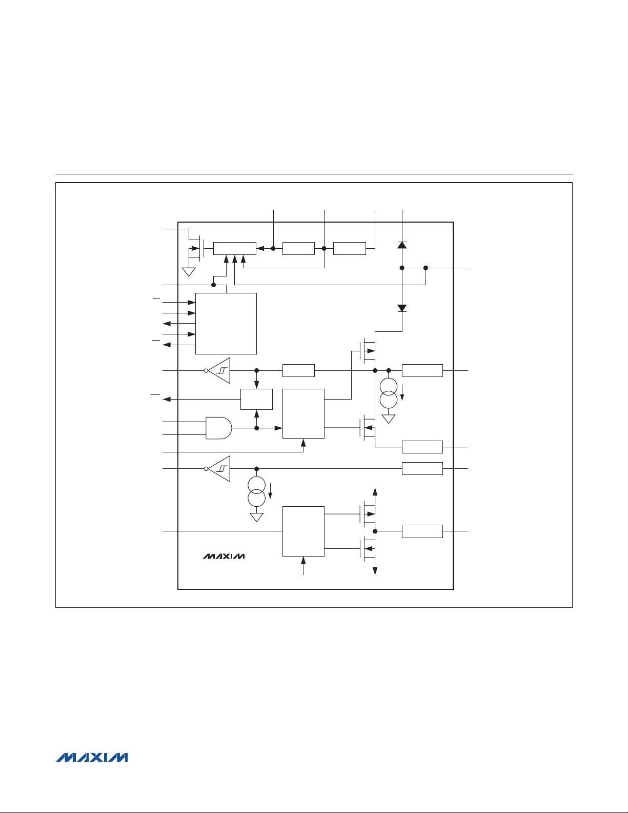
Functional Diagram
SDI
SDO
SCLK
IRQ
WU
TXQ
TXC
TXEN
DRIVER
V
5
5V LDO
V
P
PROTECTION
C/Q
LOAD
PROTECTION
PROTECTION
V
CC
C/Q
GND
DI
LDO33 LDOIN
UV
UV MONITOR
V
L
CS
STATUS
AND
CONFIGURATION
RX
WAKE-UP
DETECT
LI
3.3V LDO
FILTER
DI
LOAD
LO
MAX14821
DRIVER
DoEn
PROTECTION
DO
����������������������������������������������������������������� Maxim Integrated Products 2
Page 3
MAX14821
IO-Link Device Transceiver
ABSOLUTE MAXIMUM RATINGS
(All voltages referenced to GND, unless otherwise noted.)
VCC ......................................................................... -40V to +40V
VP (IVP < 50mA) ..... the higher of -0.3V and (VCC - 1V) to +40V
LDOIN ....................................................................-0.3V to +40V
V5 ..................... -0.3V to the lesser of (V
LDO33 ..................... -0.3V to the lesser of (V5 + 0.3V) and +6V
VL .............................................................................-0.3V to +6V
DI ...........................................................................-40V to +40V
C/Q, DO ...................... MIN: the higher of -40V and (VCC - 40V)
MAX: the lesser of +40V and (VCC + 40V)
Logic Inputs
TXC, TXQ, TXEN, LO, CS, SDI, SCLK ..... -0.3V to (VL + 0.3V)
Stresses beyond those listed under “Absolute Maximum Ratings” may cause permanent damage to the device. These are stress ratings only, and functional operation of the device at these or any other conditions beyond those indicated in the operational sections of the specifications is not implied. Exposure to absolute
maximum rating conditions for extended periods may affect device reliability.
+ 0.3V) and +6V
LDOIN
PACKAGE THERMAL CHARACTERISTICS (Note 1)
TQFN
Junction-to-Ambient Thermal Resistance (BJA) ..........36NC/W
Junction-to-Case Thermal Resistance (BJC) .................3NC/W
Note 1: Package thermal resistances were obtained using the method described in JEDEC specification JESD51-7, using a four-
layer board. For detailed information on package thermal considerations, refer to www.maxim-ic.com/thermal-tutorial.
Logic Outputs
RX, WU, LI, SDO, IRQ ............................. -0.3V to (VL + 0.3V)
UV ........................................................................-0.3V to +6V
Continuous Current Into Any Logic Pin ........................... Q50mA
Continuous Power Dissipation
TQFN (derate 27.8mW/NC above +70NC)..................2222mW
WLP (derate 22.7mW/NC above +70NC)....................1816mW
Operating Temperature Range .......................... -40NC to +85NC
Maximum Junction Temperature .....................................+150NC
Storage Temperature Range ............................ -65NC to +150NC
Lead Temperature (TQFN only; soldering, 10s) .............+300NC
Soldering Temperature (reflow) ......................................+260NC
WLP
Junction-to-Ambient Thermal Resistance (BJA) ..........44NC/W
DC ELECTRICAL CHARACTERISTICS
(VCC = 18V to 36V, VL = 2.3V to 5.5V, V
values are at VCC = 24V, VL = 3.3V, and TA = +25NC, unless otherwise noted.) (Note 2)
PARAMETER SYMBOL CONDITIONS MIN TYP MAX UNITS
VCC Supply Voltage V
VCC Supply Current I
VCC Undervoltage-Lockout
Threshold
VCC Undervoltage-Lockout
Threshold Hysteresis
V5 Supply Current I
V5 Undervoltage-Lockout
Threshold
VL Logic-Level Supply Voltage V
VL Logic-Level Supply Current I
VL Undervoltage Threshold V
5V LDO (V5)
LDOIN Input Voltage Range V
LDOIN Supply Current I
V
= 0V; all logic inputs at VL or GND; TA = -40NC to +85NC, unless otherwise noted. Typical
GND
CC
CC
V
CCUVLO
CCUVLO_HYST
5_IN
V
5UVLO
L
L
LUVLO
LDOIN
LDOIN
For driver operation 9 36 V
VCC = 24V, C/Q as input, no load on V5
or LDO33, LDOIN not connected to VP,
V
= 24V
LDOIN
VCC falling 6 7.4 9 V
LDOIN shorted to V5, external 5V applied
to V5, no switching, LDO33 disabled
V5 falling 2.0 V
All logic inputs at VL or GND 5
VL falling 0.65 0.95 1.30 V
V
= 24V, C/Q is configured as an
LDOIN
input, no load on V5 or LDO33
1 2.5 mA
200 mV
3 mA
2.3 5.5 V
FA
7 36 V
2.5 5 mA
����������������������������������������������������������������� Maxim Integrated Products 3
Page 4
IO-Link Device Transceiver
DC ELECTRICAL CHARACTERISTICS (continued)
(VCC = 18V to 36V, VL = 2.3V to 5.5V, V
values are at VCC = 24V, VL = 3.3V, and TA = +25NC, unless otherwise noted.) (Note 2)
PARAMETER SYMBOL CONDITIONS MIN TYP MAX UNITS
V5 Output Voltage Range V
V5 Load Regulation
3.3V LDO (LDO33)
LDO33 Output Voltage V
LDO33 Undervoltage-Lockout
Threshold
LDO33 Load Regulation 1mA < I
24V INTERFACE
C/Q Driver Output-Voltage High V
C/Q Driver Output-Voltage Low V
C/Q Driver Source Current Limit I
C/Q Driver Sink Current Limit I
DO Driver Output-Voltage High V
DO Driver Output-Voltage Low V
DO Driver Source Current Limit I
DO Driver Sink Current Limit I
C/Q, DI Input Voltage Range V
C/Q Input Threshold High V
C/Q Input Threshold Low V
C/Q Input Hysteresis V
DI Input Threshold High V
DI Input Threshold Low V
DI Input Hysteresis V
C/Q Weak Pulldown Current I
= 0V; all logic inputs at VL or GND; TA = -40NC to +85NC, unless otherwise noted. Typical
GND
5
No load on V5, 7V P V
1mA < I
LOAD
< 10mA, V
0.1FF bypass capacitor on V
1mA < I
LOAD
< 30mA, V
0.1FF bypass capacitor on V
LDOIN
LDOIN
LDOIN
P 36V
= 7V,
5
= 7V,
, 10W–1FF
5
compensation network added to V
LDO33
V
LDO33UVLOVLDO33
OH_C/Q
OL_C/Q
OH_C/Q
OL_C/Q
OH_DO
OL_DO
OH_DO
OL_DO
IN
IH_C/Q
IL_C/Q
HYS_C/Q
IH_DI
IL_DI
HYS_DI
PDC/Q
No load on LDO33 3.1 3.3 3.5 V
falling 2.4 V
< 20mA, V
LOAD
C/Q high-side enabled, I
= 7V 0.25 %
LDOIN
= -100mA,
C/Q
9V P VCC P 36V
C/Q low-side enabled, I
= +100mA,
C/Q
9V P VCC P 36V
C/Q high-side enabled, V
< (VCC -
C/Q
3V), 9V P VCC P 36V
C/Q low-side enabled, V
C/Q
> 3V,
9V P VCC P 36V
DO high-side enabled, IDO = +100mA,
9V P VCC P 36V
DO low-side enabled, IDO = -100mA,
9V P VCC P 36V
DO high-side enabled, VDO < (V
CC
DO high-side enabled, VDO > 3V -190 -135 -100 mA
For valid RX, LI -1.0
C/Q driver disabled 10.5 13.0 V
C/Q driver disabled 8.0 11.5 V
C/Q driver disabled 1.0 V
C/Q driver disabled, V
C/Q
= (V
CC
MAX14821
4.75 5.00 5.25 V
0.8
0.8
5
VCC -
+100 +140 +190 mA
-190 -140 -100 mA
VCC
- 3V) +100 +135 +190 mA
- 1V) 100 400
VCC –
1.3
1.3
1.4 3 V
VCC -
- 3
1.6
1.6 3 V
VCC +
1.0
6.8 8 V
5.2 6.4 V
1 V
%
V
V
V
FA
����������������������������������������������������������������� Maxim Integrated Products 4
Page 5
MAX14821
IO-Link Device Transceiver
DC ELECTRICAL CHARACTERISTICS (continued)
(VCC = 18V to 36V, VL = 2.3V to 5.5V, V
values are at VCC = 24V, VL = 3.3V, and TA = +25NC, unless otherwise noted.) (Note 2)
PARAMETER SYMBOL CONDITIONS MIN TYP MAX UNITS
DO Weak Pulldown Current I
DI Weak Pulldown Current I
C/Q Input Capacitance C
DO Input Capacitance C
DI Input Capacitance C
C/Q, DI CURRENT SINK
C/Q Load Current I
DI Load Current I
LOGIC INPUTS (TXC, TXQ, TXEN, LO, CS, SDI, SCLK)
Logic-Input Voltage Low V
Logic -Input Voltage High V
Logic-Input Leakage Current I
Logic-Input Capacitance C
LOGIC OUTPUTS (RX, WU, LI, UV, SDO, IRQ)
Logic-Output Voltage Low V
Logic-Output Voltage High
V
SDO Leakage Current I
THERMAL SHUTDOWN
Thermal Warning Threshold Die temperature rising, OTemp bit is set +115
Thermal Warning Threshold
Hysteresis
Thermal Shutdown Threshold Die temperature rising +150
Thermal Shutdown Hysteresis 20
= 0V; all logic inputs at VL or GND; TA = -40NC to +85NC, unless otherwise noted. Typical
GND
PDDO
LLM_C/Q
LLM_DI
V
OHRX
OHWU
V
OHSDO,
V
OHIRQ
LK_SDO
PDDI
C/Q
DO
DI
IL
IH
LEAK
IN
OL
, V
DO driver disabled, V
VDO = (V
CC
- 1V)
DI load disabled, V
VDI = (V
CC
- 1V)
C/Q driver disabled 40 pF
DO driver disabled 40 pF
C/Q load enabled
(C/QLoad = 1)
DI load enabled
(DiLoad = 1)
Logic input = GND or V
I
= -5mA 0.4 V
OUT
,
,
OHLI
I
= 5mA (Note 3)
OUT
,
SDO disabled, SDO = GND or V
CC
CC
= 36V,
L
= 36V,
0V P V
5V P V
C/Q
C/Q
P 5V
0V P VDI P 5V
9V P V
DI
L
40 120
50 300
0 9
5 6.6 9
0 9
6 7.5 9
0.3 x
V
L
-1 +1
VL -
0.6
-1 +1
Die temperature falling, OTemp bit is
cleared
FA
FA
20 pF
mA
mA
0.7 x
V
L
FA
5 pF
FA
NC
20
NC
NC
NC
V
V
V
����������������������������������������������������������������� Maxim Integrated Products 5
Page 6
IO-Link Device Transceiver
AC ELECTRICAL CHARACTERISTICS
(VCC = 18V to 36V, VL = 2.3V to 5.5V, V
values are at VCC = 24V, VL = 3.3V, and TA = +25NC, unless otherwise noted.) (Note 2)
PARAMETER SYMBOL CONDITIONS MIN TYP MAX UNITS
C/Q, DO, DI INTERFACES
Data Rate DR
DRIVER (C/Q, DO)
Driver Low-to-High Propagation
Delay
Driver High-to-Low Propagation
Delay
Driver Skew t
Driver Rise Time t
Driver Fall Time t
Driver Enable Time High t
Driver Enable Time Low t
Driver Disable Time High t
Driver Disable Time Low t
RECEIVER (C/Q, DI) (Figure 4)
Receiver Low-to-High
Propagation Delay
Receiver High-to-Low
Propagation Delay
WAKE-UP DETECTION (Figure 5)
Wake-Up Input Minimum Pulse
Width
Wake-Up Input Maximum Pulse
Width
WU Output Low Time
= 0V; all logic inputs at VL or GND; TA = -40NC to +85NC, unless otherwise noted. Typical
GND
HiSlew = 1 4.8 230.4
HiSlew = 0 4.8 38.4
t
PDLH
t
PDHL
SKEW
RISE
FALL
ENH
ENL
DISH
DISL
t
PRLH
t
PRHL
t
WUMIN
t
WUMAX
t
WUL
Push-pull or high-side (PNP)
configuration, Figure 1
Push-pull or low-side (NPN)
configuration, Figure 1
|t
- t
PDLH
Push-pull or high-side (PNP)
configuration, Figure 1
Push-pull or low-side (NPN)
configuration, Figure 1
Push-pull or high-side (PNP)
configuration, Figure 3
Push-pull or low-side (NPN)
configuration, Figure 2
Push-pull or high-side (PNP)
configuration, Figure 2
(Note 4)
Push-pull or low-side (NPN)
configuration, Figure 3
(Note 4)
RxFilter = 1 0.2 2
RxFilter = 0 0.4 2
RxFilter = 1 0.3 2
RxFilter = 0 0.5 2
Valid wake-up condition on C/Q 120 190 260
| 0.1 2
PDHL
HiSlew = 1 0.5 2
HiSlew = 0 1.6 5
HiSlew = 1 0.5 2
HiSlew = 0 1.6 5
HiSlew = 1 0.4 1.7
HiSlew = 0 1.5 4
HiSlew = 1 0.4 1.7
HiSlew = 0 1.4 4
HiSlew = 1 0.3 1
HiSlew = 0 0.8 7
HiSlew = 1 0.3 1
HiSlew = 0 0.9 7
HiSlew = 1 1.6 3
HiSlew = 0 1.6 3
HiSlew = 1 0.1 3
HiSlew = 0 0.1 3
MAX14821
30 40 50
120 140 160
kbps
Fs
Fs
Fs
Fs
Fs
Fs
Fs
Fs
Fs
Fs
Fs
Fs
Fs
Fs
����������������������������������������������������������������� Maxim Integrated Products 6
Page 7
MAX14821
IO-Link Device Transceiver
AC ELECTRICAL CHARACTERISTICS (continued)
(VCC = 18V to 36V, VL = 2.3V to 5.5V, V
values are at VCC = 24V, VL = 3.3V, and TA = +25NC, unless otherwise noted.) (Note 2)
PARAMETER SYMBOL CONDITIONS MIN TYP MAX UNITS
SPI TIMING (CS, SCLK, SDI, SDO) (Figure 6)
SCLK Clock Period t
SCLK Pulse-Width High t
SCLK Pulse-Width Low t
CS Fall to SCLK Rise Time
SCLK Rise to CS Rise Hold Time
SDI Hold Time t
SDI Setup Time t
Output Data Propagation Delay t
SDO Rise and Fall Times t
Minimum CS Pulse
Note 2: All devices are 100% production tested at TA = +25NC. Limits over the operating temperature range are guaranteed by
design.
Note 3: UV is an open-drain output. Connect UV to a voltage less than 5.5V through an external pullup resistor.
Note 4: Disable time measurements are load dependent.
= 0V; all logic inputs at VL or GND; TA = -40NC to +85NC, unless otherwise noted. Typical
GND
CH+CL
CH
CL
t
CSS
t
CSH
DH
DS
DO
FT
t
CSW
83.3 ns
41.65 ns
41.65 ns
20 ns
20 ns
10 ns
10 ns
32 ns
20 ns
76.8 ns
����������������������������������������������������������������� Maxim Integrated Products 7
Page 8
TXEN
(TXC AND TXQ)
OR LO
OR DO
C/Q
IO-Link Device Transceiver
TXEN
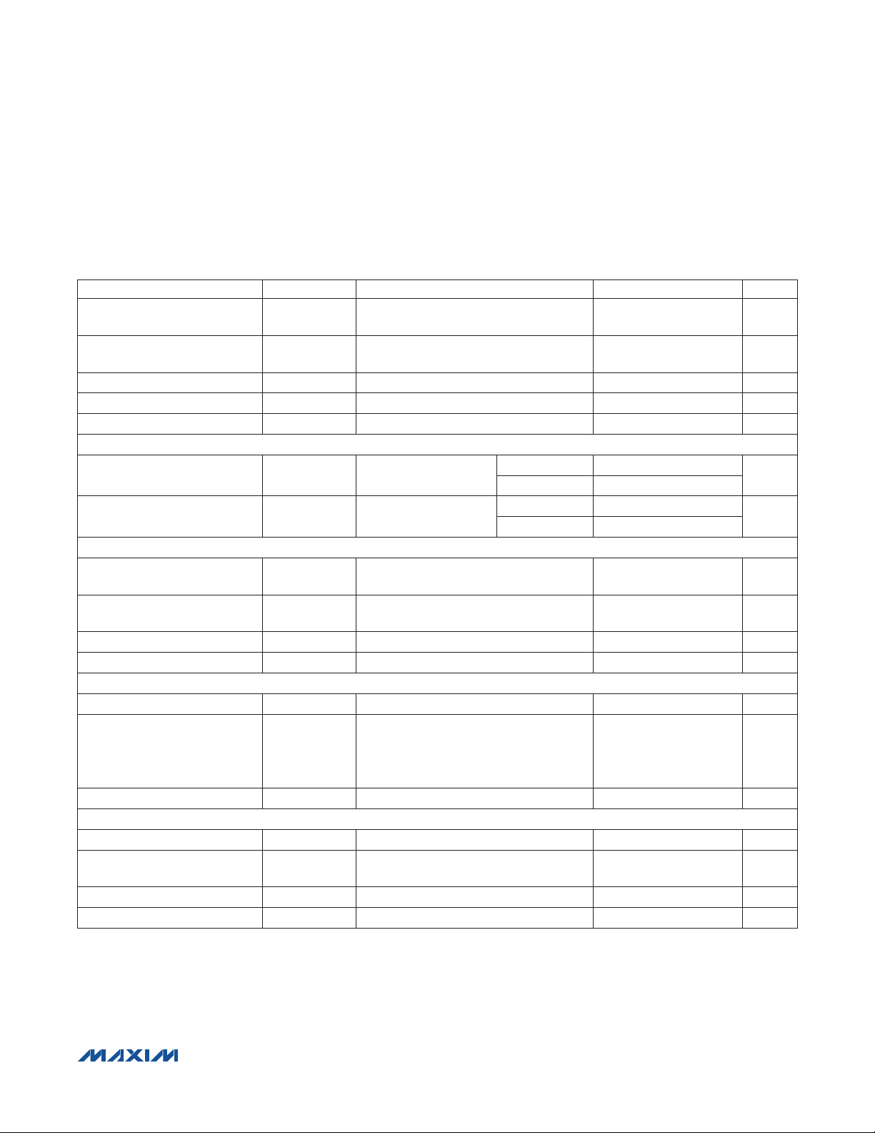
TXC C/Q OR DO
t
FALL
MAX14821
GND
t
TXQ
LO
PDHL
t
RISE
3.3nF 5kΩ
50%
t
PDLH
MAX14821
V
L
0V
V
L
0V
V
90%
50%
10%
CC
0V
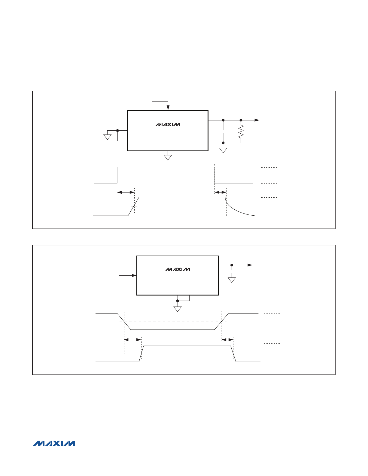
Figure 1. C/Q and LO Driver Propagation Delays and Rise/Fall Times
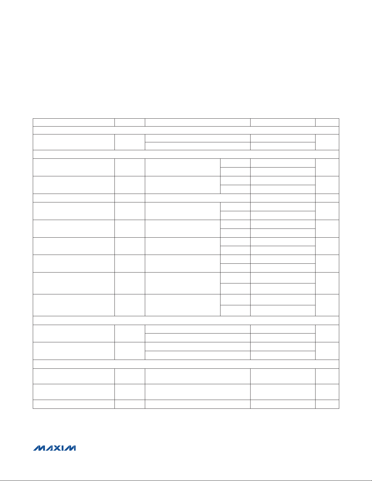
TXEN
C/Q
V
L
TXC
TXQ
t
ENL
10%
TXEN
MAX14821
GND
C/Q
t
DISH
Figure 2. C/Q Driver Enable Low and Disable High Timing with External Pullup Resistor
V
CC
10%
5kΩ
3.3nF
V
L
0V
V
CC
0V
����������������������������������������������������������������� Maxim Integrated Products 8
Page 9
TXEN
TXC
TXQ
MAX14821
IO-Link Device Transceiver
TXEN
C/Q
MAX14821
GND
3.3nF 5kΩ
V
L
t
ENH
C/Q
90%
Figure 3. C/Q Driver Enable High and Disable Low Timing
C/Q OR DI
OR DI
C/Q
t
PRLH
OR LI
RX
MAX14821
GND
TXEN
RX OR LI
t
DISL
t
PRHL
90%
50%
15pF
50%
0V
V
CC
0V
V
CC
0V
V
L
0V
Figure 4. C/Q and DI Receiver Propagation Delays
����������������������������������������������������������������� Maxim Integrated Products 9
Page 10

TXEN
TXC AND TXQ
C/Q
TXC AND TXQ
MAX14821
IO-Link Device Transceiver
TXEN
WU
MAX14821
C/Q
GND
< t
WUMIN
NO WAKE-UP
t
< tWU < t
WUMIN
WUMAX
WU
NOTE: THE MAX14821 RECOGNIZES A WAKE-UP PULSE WHEN C/Q IS SHORTED FROM HIGH-TO-LOW OR FROM LOW-TO-HIGH FOR t
Figure 5. Wake-Up Detection Timing
CS
t
CSS
t
DS
t
DH
SCLK
SDI
SDO
t
CSH
t
WUL
< tWU < t
WUMIN
t
t
CL
CH
t
DO
t
CSH
WUMAX
.
Figure 6. SPI Timing Diagram
���������������������������������������������������������������� Maxim Integrated Products 10
Page 11

MAX14821
IO-Link Device Transceiver
Typical Operating Characteristics
(VCC = 24V, LDOIN = VP, VL = LDO33, C/Q and DO in push-pull configuration, TA = +25NC, unless otherwise noted.)
C/Q DRIVER OUTPUT HIGH
vs. LOAD CURRENT
24
23
22
(V)
21
OH_C/Q
V
20
19
18
0 175
TA = -40°C
TA = +25°C
LOAD CURRENT (mA)
DO DRIVER OUTPUT HIGH
vs. LOAD CURRENT
24
TA = +85°C
TA = +25°C
(V)
OH_DO
V
23
22
TA = -40°C
21
20
19
TA = +85°C
150125100755025
MAX14821 toc01
MAX14821 toc03
C/Q DRIVER OUTPUT LOW
vs. SINK CURRENT
7
6
5
(V)
4
OL_C/Q
3
V
2
1
0
0 175
TA = +85°C
TA = +25°C
TA = -40°C
SINK CURRENT (mA)
DO DRIVER OUTPUT LOW
vs. SINK CURRENT
7
6
5
(V)
4
OL_DO
3
V
2
1
TA = +85°C
TA = +25°C
TA = -40°C
MAX14821 toc02
150125100755025
MAX14821 toc04
18
0 175
LOAD CURRENT (mA)
C/Q DRIVER PROPAGATION DELAY
vs. TEMPERATURE (HiSlew = 0)
1.30
1.28
1.26
1.24
1.22
(µs)
1.20
PDHL
t
1.18
1.16
1.14
TXEN = V
TXC = TXQ
L
TEMPERATURE (°C)
1.12
1.10
-45 90
150125100755025
MAX14821 toc05
756030 45-15 0 15-30
0
0 175
SINK CURRENT (mA)
C/Q DRIVER PROPAGATION DELAY
vs. TEMPERATURE (HiSlew = 1)
0.46
0.45
0.44
0.43
(µs)
0.42
PDHL
t
0.41
0.40
0.39
TXEN = V
L
TXC = TXQ
0.38
-45 90
TEMPERATURE (°C)
150125100755025
MAX14821 toc06
7560-30 -15 0 3015 45
���������������������������������������������������������������� Maxim Integrated Products 11
Page 12

MAX14821
IO-Link Device Transceiver
Typical Operating Characteristics (continued)
(VCC = 24V, LDOIN = VP, VL = LDO33, C/Q and DO in push-pull configuration, TA = +25NC, unless otherwise noted.)
C/Q DRIVER OUTPUT SWITCHING
(HiSlew = 0)
V
TXC=TXQ
2V/div
0V
V
C/Q
5V/div
0V
2µs/div
RECEIVER PROPAGATION DELAY
vs. TEMPERATURE (RxFilter = 0)
550
500
450
400
DI TO LI
350
(ns)
PRHL
t
C/Q TO RX
300
250
200
150
100
-45 90
TEMPERATURE (°C)
MAX14821 toc07
756030 45-15 0 15-30
Ch1 Ch2
1.430µs
Ch1 Ch2
1.330µs
Ch2 RISE
1.583µs
Ch2 FALL
1.455µs
MAX14821 toc09
C/Q DRIVER OUTPUT SWITCHING
(HiSlew = 1)
V
TXC=TXQ
2V/div
0V
V
C/Q
5V/div
0V
2µs/div
RECEIVER PROPAGATION DELAY
vs. TEMPERATURE (RxFilter = 1)
400
350
300
250
(ns)
200
PRHL
t
DI TO LI
150
C/Q TO RX
100
50
0
-45 90
TEMPERATURE (°C)
MAX14821 toc08
7560-30 -15 0 3015 45
Ch1 Ch2
357.1ns
Ch1 Ch2
335.4ns
Ch2 RISE
343.5ns
Ch2 FALL
331.7ns
MAX14821 toc10
WAKE-UP DETECTION
40µs/div
MAX14821 toc11
V
C/Q
10V/div
0V
V
WU
2V/div
0V
C/Q SHORT-CIRCUIT PROTECTION
TXEN = V
L
TXC = TXQ = GND
t
= 200µs
SHORT
40µs
MAX14821 toc12
C/Q
10V/div
I
SOURCE
100mA/div
IRQ
2V/div
���������������������������������������������������������������� Maxim Integrated Products 12
Page 13

MAX14821
IO-Link Device Transceiver
Typical Operating Characteristics (continued)
(VCC = 24V, LDOIN = VP, VL = LDO33, C/Q and DO in push-pull configuration, TA = +25NC, unless otherwise noted.)
C/Q SHORT-CIRCUIT PROTECTION
TXEN = V
L
TXQ = TXC = V
t
SHORT
= 200µs
L
40µs
V5 LOAD REGULATION
0
-0.05
-0.10
-0.15
-0.20
-0.25
-0.30
% VOLTAGE CHANGE
-0.35
-0.40
-0.45
-0.50
0 50
TA = +25°C
TA = +85°C
LOAD CURRENT (mA)
MAX14821 toc13
TA = -40°C
40302010
C/Q
10V/div
I
SINK
100mA/div
IRQ
2V/div
MAX14821 toc15
DO SHORT-CIRCUIT PROTECTION
DO DRIVER ENABLED
LO = GND
t
= 500µs
SHORT
100µs
LDO33 LOAD REGULATION
0
-0.1
-0.2
-0.3
-0.4
% VOLTAGE CHANGE
-0.5
-0.6
-0.7
0 50
TA = +25°C
LOAD CURRENT (mA)
TA = -40°C
TA = +85°C
MAX14821 toc14
40 4535302520155 10
DO
10V/div
I
SOURCE
100mA /div
IRQ
2V/div
MAX14821 toc16
VCC SUPPLY CURRENT
VOLTAGE
vs. V
1.8
1.6
1.4
1.2
1.0
(mA)
CC
I
0.8
0.6
V
LDOIN
C/Q AND DO DRIVERS ENABLED
0.4
V5, VP UNLOADED
C/Q AND DI CURRENT LOADS OFF
0.2
TXC = TXQ = LO = V
0
9 36
CC
TA = +25°C
TA = +85°C
= 7V
L
VCC VOLTAGE (V)
TA = -40°C
4.0
(mA)
LDOIN
I
3.5
3.0
2.5
2.0
1.5
1.0
0.5
0
MAX14821 toc17
333024 2715 18 2112
LDOIN SUPPLY CURRENT
vs. LDOIN VOLTAGE
TA = -40°C
VCC = 36V
C/Q AND DO DRIVERS ENABLED
V5, LDO33 ARE LOADED
TXC = TXQ = LO = V
9 36
TA = +25°C
L
V
LDOIN
TA = +85°C
333012 15 18 2421 27
(V)
MAX14821 toc18
���������������������������������������������������������������� Maxim Integrated Products 13
Page 14
MAX14821
IO-Link Device Transceiver
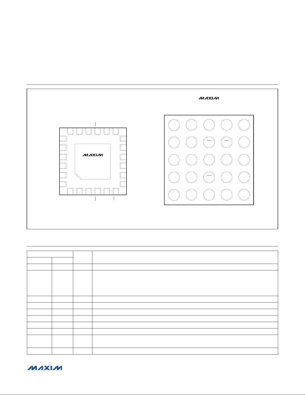
Pin/Bump Configurations
TOP VIEW
(BUMP SIDE DOWN)
MAX14821
1 2 3 4
TOP VIEW
DI
19
GND
20
C/Q
21
22
DO
V
23
CC
24
V
P
LI
LO
1718 16 14 13
15
MAX14821
+
1 2
LDOIN
5
V
3
LDO33
4 5 6
WU
IRQ
RXUVTXEN
*EP
SCLK
12
TXC
TXQ
11
I.C.
10
9
V
L
SDI
8
SDO
7
CS
+
CC
DI
LDOIN V
A
V
B
C/Q
C
GND
D
DO
E
TQFN
*CONNECT EXPOSED PAD TO GND.
PIN
TQFN-EP WLP
1 A2 LDOIN
NAME FUNCTION
5V Linear Regulator Input. Bypass LDOIN to GND with a 0.1FF ceramic capacitor.
5V Power-Supply Input and 5V Linear Regulator Output. Bypass V5 to GND with a 0.1FF
2 A3 V
ceramic capacitor for 10mA load capability. Add the recommended compensation network
5
to increase the source capability to 30mA. See the 5V and 3.3V Linear Regulators section for
more information.
3 A4 LDO33
4 B3
IRQ Active-Low Interrupt Request Output. IRQ is a push-pull output referenced to VL.
3.3V Linear Regulator Output. Bypass LDO33 to GND with a 1FF ceramic capacitor.
5 A5 SCLK SPI Clock Input
6 B4
CS
Active-Low SPI Chip-Select Input
7 B5 SDO SPI Serial-Data Output
8 C4 SDI SPI Serial-Data Input
9 C5 V
Logic-Level Supply Input. VL defines the logic levels on all the logic inputs and outputs.
L
Bypass VL to GND with a 0.1FF ceramic capacitor.
10 C3 I.C. Internally Connected. Connect to VL or leave unconnected.
5
LDO33 SCLK
5
V
P
GND I.C. SDI V
UV TXC TXQ
LI LO RX TXEN
IRQ SDO
WU
CS
L
WLP
Pin/Bump Descriptions
���������������������������������������������������������������� Maxim Integrated Products 14
Page 15
MAX14821
IO-Link Device Transceiver
Pin/Bump Descriptions (continued)
PIN
TQFN-EP WLP
11 D5 TXQ
12 D4 TXC
13 E5 TXEN Transmitter Enable. Drive TXEN high to enable the C/Q transmitter. TXEN is referenced to VL.
14 E4 RX
15 D3
16 E3 LO Logic Input of the DO Output. LO is the logic input that drives DO. LO is referenced to VL.
17 E2 LI Logic Output of the 24V DI Logic Input. LI is the inverse logic of DI. LI is referenced to VL.
18 D2 UV
19 E1 DI 24V Logic-Level Digital Input
20 C1, C2 GND Ground
21 B1 C/Q
22 D1 DO
23 A1 V
24 B2 V
— — EP Exposed Pad (TQFN Only). Connect EP to GND.
NAME FUNCTION
Transmit Level Input. The logic on the C/Q output is the inverse logic level of the signals on
the TXC and TXQ inputs. TXQ is ANDed with TXC. Drive TXQ high if not in use.
Transmit Communication Input. The logic on the C/Q output is the inverse logic level of the
signals on the TXC and TXQ inputs. TXC is ANDed with TXQ. Drive TXC high if not in use.
Receiver Output. RX is the inverse logic level of C/Q. RX is always high when the RxDis bit in
the CQConfig register is set to 1.
WU
Active-Low Wake-Up Output. WU is a push-pull output referenced to VL. WU pulses low for
190Fs (typ) when a valid wake-up pulse is detected on the C/Q line.
Open-Drain Undervoltage Indicator Output. In case of an undervoltage, the UV open-drain
transistor is off.
SIO/IO-Link Data Input/Output. Drive TXEN high to enable the C/Q driver. The logic on the
C/Q output is the inverse logic level of the signals on the TXC and TXQ inputs. RX is the logic
inverse of C/Q. The C/Q driver output level can be set by the TXC/TXQ inputs or programmed
by the Q bit. The level on C/Q can be read by the RX ouput or the QLvl bit.
24V Logic-Level Digital Output. DO is the inverse logic level of the LO input and can be digi-
tally controlled through the DIOConfig register.
Power-Supply Input. Bypass VCC to GND with a 1FF ceramic capacitor.
CC
Protected 24V Supply Output. VP is one diode drop below VCC. VP is reverse-polarity protect-
P
ed and can be used as a 24V protected supply to the sensor or actuator electronics.
���������������������������������������������������������������� Maxim Integrated Products 15
Page 16

MAX14821
IO-Link Device Transceiver
Detailed Description
The MAX14821 is a sensor/actuator transceiver designed
for IO-Link device applications supporting all the specified IO-Link data rates. In IO-Link applications, the
device acts as the physical layer interface to a microcontroller running the data-link layer protocol. The device
contains an additional 24V digital input and an additional
24V digital output. Two internal linear regulators generate common sensor and actuator power requirements:
5V and 3.3V.
The device detects IO-Link wake-up conditions on the C/Q
line and generates a wake-up signal on the WU output.
The C/Q and DO drivers are independently configurable to
any one of three driver output types: push-pull, high-side
(PNP), or low-side (NPN).
The C/Q and DI inputs have selectable current sinks that
can be enabled for use in actuators where the master
requires a Type 2 load. The device is configured and
monitored through an SPI interface. Extensive alarms are
available through SPI.
24V Interface
The device features an IO-transceiver interface capable
of operating with voltages up to 36V. This is the 24V interface and includes the C/Q input/output, the logic-level
digital output (DO), and the logic-level digital input (DI).
Configurable Drivers
The device features selectable push-pull, high-side (PNP),
or low-side (NPN) switching drivers at C/Q and DO.
Set the C/Q_N/P and C/Q_PP bits in the CQConfig register to select the driver mode for the C/Q driver. When
configured as a push-pull output, C/Q switches between
VP and ground. Set the C/Q_PP bit to 1 to select pushpull operation at C/Q. Set the C/Q_PP bit to 0 to configure
the C/Q output for open-drain operation. The C/Q_N/P bit
selects NPN or PNP operation when C/Q is configured as
an open-drain output.
Set the DoN/P and DoPP bits in the DIOConfig register
to select the driver mode for the DO output. When configured as a push-pull output, DO switches between VCC
and ground. Set the DoPP bit to 1 for push-pull operation.
The DoN/P bit selects NPN or PNP operation when DO is
configured as an open-drain output. Set the DoPP bit to 0
to select high-side or low-side operation at DO.
C/Q Driver and Receiver
The TXEN input enables the C/Q driver. Drive TXEN high
to enable the C/Q driver. Drive TXEN low to disable the
driver.
The C/Q driver is specified to supply up to 100mA DC
load current.
The HiSlew bit increases the slew rate of the C/Q and DO
driver outputs. Set HiSlew to 1 for data rates of 230kbps
or higher. Set HiSlew to 0 to reduce both the C/Q and DO
driver slew rates to reduce EMI emission and reflections.
The C/Q receiver is always on. Disable the RX output
through the RxDis bit in the CQConfig register. Set the
RxDis bit to 1 to set the RX output high. Set the RxDis bit
to 0 for normal receive operation.
The C/Q receiver has an analog lowpass filter to reduce
high-frequency noise present on the line. Set the RxFilter
bit in the CQConfig register to 0 to set the filter corner
frequency to 500kHz (typ). Set the RxFilter bit to 1 to set
the corner frequency of the filter to 1MHz (typ). Noise
filters are present on both the C/Q and DI receivers and
are controlled simultaneously by the RxFilter bit.
C/Q Fault Detection
The device registers a C/QFault condition under either of
two conditions:
1) When it detects a short circuit for longer than 160µs
(typ). A short condition exists when the C/Q driver’s
load current exceeds the 140mA (typ) current limit.
2) When it detects a voltage level error at the C/Q output. A voltage level error occurs when the C/Q driver
is configured for open-drain operation (NPN or PNP),
the driver is turned off, and the C/Q voltage is not
pulled to exceed the C/Q receiver’s threshold levels
(< 8V or > 13V) by the external supply.
When a C/QFault error occurs, the C/QFault and
C/QFaultInt bits are set, IRQ asserts, and the driver is
turned off 240µs (typ) after the start of the fault condition.
When a short-circuit event occurs on C/Q, the driver
enters autoretry mode. In autoretry mode the device
periodically checks whether the short is still present and
attempts to correct the driver output. Autoretry attempts
last for 350µs (typ) and occur every 26ms (typ).
���������������������������������������������������������������� Maxim Integrated Products 16
Page 17

MAX14821
IO-Link Device Transceiver
DO Fault Detection
The device registers a DoFault event when a short circuit
is present at the DO output for longer than 30–440Fs. A
short condition exists when the load current on the DO
driver exceeds the 135mA (typ) DO current limit. When a
short-circuit condition is detected, the DO driver enters
autoretry mode. In autoretry mode the device periodically checks whether the error is still present. Autoretry
attempts last for 440µs (typ) and occur every 26ms
(typ). When a DoFault error is detected, the DoFault and
DoFaultInt bits are set, IRQ asserts, and the driver is
turned off 440µs (typ) after the start of the DO faults.
Reverse-Polarity Protection
The device is protected against reverse-polarity connections on VCC, C/Q, DO, DI, and GND. Any combination
of these pins can be connected to DC voltages up to
40V (max). A short to 40V results in a current flow of less
than 500FA.
Ensure that the maximum voltage between any of these
pins does not exceed 40V.
5V and 3.3V Linear Regulators
The device includes two internal current-limited regulators
to generate 5V (V5) and 3.3V (LDO33). V5 is specified at
10mA when bypassed with a 0.1µF capacitor to ground.
Add the compensation network shown in Figure 7 to draw
up to 30mA from V5. LDO33 is specified at 20mA. The
input of V5, LDOIN, can be connected to VP, the protected 24V supply output, or to another voltage in the 7V
to 36V range.
V5 constitutes the supply for the logic block. The 5V LDO
can be disabled by connecting LDOIN to V5. Apply an
external voltage from 4.75V to 5.25V to V5 when the LDO
is disabled.
Use the LDO33Dis bit in the Mode register to enable/
disable LDO33. See the Mode Register [R1, R0] = [1,1]
section for more information. V5 and LDO33 are not protected against short circuits.
Power-Up
The C/Q and DO driver outputs and the UV output are
high impedance when VCC, V5, VL, and/or LDO33 voltages are below their respective undervoltage thresholds during power-up. UV goes low and the drivers are
enabled when all these voltages exceed their respective
undervoltage-lockout thresholds.
The drivers are automatically disabled if VCC, V5, or VL
falls below its threshold.
Undervoltage Detection
The device monitors VCC, V5, VL, and optionally LDO33
for undervoltage conditions. UV is high impedance when
any monitored voltage falls below its UVLO threshold.
VCC, V5, and VL undervoltage detection cannot be disabled. When VCC falls below the V
CCUVLO
threshold, the
UV24 and UV24Int bits are set, UV asserts high, and IRQ
asserts low.
The SPI register contents are unchanged while V5 is present, regardless of the state of VCC and LDO33. The SPI
interface is not accessible and IRQ is not available when
UV is asserted due to a V5 or VL undervoltage event.
When the internal 3.3V LDO regulator voltage (V
LDO33
falls below the LDO33 undervoltage-lockout threshold,
the UV33Int bit in the Status register is set and IRQ
asserts. UV asserts if the UV33En bit in the Mode register
is set to 1.
The UV output deasserts once the undervoltage condition is removed; however, bits in the Status register and
the IRQ output are not cleared until the Status register
has been read.
)
V
5
MAX14821
LDO33 3.3V
V
L
Figure 7. V5 Compensation Network
���������������������������������������������������������������� Maxim Integrated Products 17
0.1µF
1µF
10Ω
1µF
5V
The device detects an IO-Link wake-up condition on the
Wake-Up Detection
C/Q line in push-pull, high-side (PNP), or low-side (NPN)
operation modes. A wake-up condition is detected when
the C/Q output is shorted for 80Fs (typ). WU pulses low
for 190Fs (typ) when the device detects a wake-up pulse
on C/Q (Figure 5).
Set the WuIntEn bit in the Mode register to set the WuInt
bit in the Status register and generate an interrupt on
IRQ when a wake-up pulse is detected. WuInt is set
and IRQ asserts immediately after C/Q is released when
WuIntEn = 1.
Page 18

MAX14821
IO-Link Device Transceiver
Thermal Protection and Considerations
The internal LDOs and drivers can generate more power
than the package for the device can safely dissipate.
Ensure that the driver LDO loading is less than the package can dissipate. Total power dissipation for the device
is calculated using the following equation:
P
where P
= P
TOTAL
is the power generated in the C/Q driver,
C/Q
+ PDO + P5 + P
C/Q
P
+ P
CLCQ
CLDI
LDO33
+ PQ +
PDO is the power dissipated by the DO driver, P5 and
P
quiescent power generated by the device, and P
and P
are the power generated by the LDOs, PQ is the
LDO33
are the power generated in the C/Q and DI
CLDI
CLCQ
current sinks.
Ensure that the total power dissipation is less than the
limits listed in the Absolute Maximum Ratings section.
Use the following to calculate the power dissipation (in
mW) due to the C/Q driver:
P
C/Q
= [I
(max)] × [0.5 + 7 × I
C/Q
C/Q
(max)]
Calculate the internal power dissipation of the DO driver
using the following equation:
PDO = [IDO(max)] × [0.5 + 7 × IDO(max)]
Calculate the power dissipation in the 5V LDO, V5, using
the following equation:
P5 = (V
where I5 includes the I
LDOIN
LDO33
- V5) × I
5
current sourced from
LDO33.
Calculate the power dissipated in the 3.3V LDO, LDO33,
using the following equation:
P
LDO33
= 1.7V × I
LDO33
Calculate the quiescent power dissipation in the device
using the following equation:
PQ = 5mA × VCC(max)
If the current sinks are enabled, calculate their associated power dissipation as:
P
= 7mA × V
CLCQ
P
= 7mA × VDI(max)
CLDI
C/Q
(max)
Overtemperature Warning
Bits in the Status and Mode registers are set when the
temperature of the device exceeds +115NC (typ). The
OTempInt bit in the Status register is set and IRQ asserts
when the OTemp bit in the Mode register is set. Read the
Status register to clear the OTempInt bit and IRQ.
The OTemp bit is cleared when the die temperature falls
to +95NC.
The device continues to operate normally unless the
die temperature reaches the +150NC thermal shutdown
threshold, when the device enters thermal shutdown.
Thermal Shutdown
All regulators and the C/Q and DO output drivers are
automatically switched off when the internal die temperature exceeds the +150NC (typ) thermal shutdown threshold. SPI communication is not available during a thermal
shutdown event.
Regulators are automatically switched on when the internal die temperature falls below the thermal shutdown
threshold plus hysteresis. The internal registers return to
their default state when the V5 regulator is switched on.
���������������������������������������������������������������� Maxim Integrated Products 18
Page 19

MAX14821
IO-Link Device Transceiver
Register Functionality
The device has four 8-bit-wide registers for configuration and monitoring (Table 1).
Table 1. Register Summary
REGISTER R1 R0 D7 D6 D5 D4 D3 D2 D1 D0
Status 0 0 WuInt DoFaultInt DiLvl
CQConfig 0 1 RxFilter HiSlew C/Q_N/P C/Q_PP C/QDEn Q RxDis C/QLoad
DIOConfig 1 0 DoInv DoAv DoN/P DoPP DoEn DoBit LiDis DiLoad
Mode 1 1 RST WuIntEn DoFault C/QFault UV24 OTemp UV33En LDO33Dis
R1/R0 = Register address.
Bit D7 D6 D5 D4 D3 D2 D1 D0
Bit Name
Read/Write
POR State
Reset Upon Read
X = Unknown. These bits are dependent on the DI logic and C/Q inputs.
WuInt DoFaultInt DiLvl
R R R R R R R R
0 0 X X 0 0 0 0
Yes Yes No No Yes Yes Yes Yes
QLvl
QLvl
C/QFaultInt UV33Int UV24Int OTempInt
Status Register [R1, R0] = [0,0]
C/QFaultInt UV33Int UV24Int OTempInt
The Status register reflects the logic levels of C/Q and DI and shows the source of interrupts that cause an IRQ
hardware interrupt. The IRQ interrupt is asserted when an alarm condition (OTemp, UV33Int, UV24, C/QFault,
DoFault, WuInt) is detected. All bits in the Status register are read-only. The interrupt bits return to the default state
after the Status register is read. If a C/Q or DO fault condition persists, the associated interrupt bits are immediately
set after the Status register is read.
BIT NAME DESCRIPTION
D7 Wulnt Wake-Up Interrupt Request. WuInt is set when an IO-Link wake-up request pulse is
detected on C/Q and the WuIntEn bit in the Mode register is set. IRQ asserts when
WuInt is set to 1. Read the Status register to clear the WuInt bit and deassert IRQ.
D6 DoFaultInt DO Fault Interrupt. DoFaultInt interrupt bit and DoFault bit (in the Mode register) are
D5 DiLvl DI Logic Level. The DiLvl bit mirrors the current logic level at the DI input. It is the
set when a fault condition occurs on the DO driver output. The device registers a fault
condition when a short circuit or voltage fault is detected on DO (see the DO Fault
Detection section for more information). IRQ asserts when DoFaultInt is 1. Read the
Status register to clear the DoFaultInt bit and deassert IRQ.
inverse of the LI output and is always active regardless of the state of the LiDis bit (Table
2). DiLvl does not affect IRQ. DiLvl is not changed when the Status register is read.
���������������������������������������������������������������� Maxim Integrated Products 19
Page 20

IO-Link Device Transceiver
BIT NAME DESCRIPTION
MAX14821
D4
D3 C/QFaultInt C/Q Fault Interrupt. The C/QFaultInt interrupt bit and C/QFault bit (in the Mode register)
D2 UV33Int Internal 3.3V LDO (LDO33) Undervoltage Warning. Both the UV33Int interrupt bit and
D1 UV24Int VCC Undervoltage Interrupt. The UV24Int interrupt bit and the UV24 bit (in the Mode
D0 OTempInt Overtemperature Warning. The OTempInt interrupt bit and the OTemp bit (in the Mode
QLvl C/Q Logic Level. The QLvl bit is the inverse of the logic level at C/Q. QLvl is 1 when the
C/Q input level is low (< 8V) and is 0 when the C/Q logic level is high (> 13V) (Table 3).
QLvl remains active when the C/Q receiver is disabled (RxDis = 1). QLvl does not affect
IRQ. QLvl is not changed when the Status register is read.
are set when a short circuit or voltage fault occurs on the C/Q driver output (see the C/Q
Fault Detection section for more information). IRQ asserts when C/QFault is 1. Read the
Status register to clear the C/QFaultInt bit and deassert IRQ.
the UV33En bit (in the Mode register) are set when V
undervoltage threshold. If UV33En is set in the Mode register, IRQ asserts low when the
UV33Int bit is 1. Read the Status register to clear the UV33Int bit and deassert IRQ.
Set the UV33En bit to 1 in the Mode register to enable undervoltage monitoring for
UV33Int. When enabled, UV asserts high when the UV33Int bit is 1. UV deasserts when
V
rises above the LDO33 undervoltage threshold.
LDO33
register) are set when the VCC voltage falls below the 7.4V undervoltage threshold. IRQ
asserts low when the UV24Int bit is 1. Read the Status register to clear the UV24Int bit
and deassert IRQ. VCC undervoltage detection cannot be disabled.
register) are set when a high-temperature condition is detected by the device. OTemp
is set when the temperature of the die exceeds +115NC (typ). OTempInt is set and IRQ
asserts when the OTemp bit is 1. The OTempInt bit is cleared and IRQ deasserts when
the Status register is read.
Once cleared, OTempInt is not reset if the die temperature remains above the thermal
warning threshold and does not fall below +95°C.
falls below the 2.4V LDO33
LDO33
Table 2. DiLvl and LI Output Table 3. QLvl and RX Output
V
(V) DiLvl BIT LI OUTPUT
DI
< 5.2 0 High
> 8 1 Low
���������������������������������������������������������������� Maxim Integrated Products 20
V
(V)
C/Q
< 8 1 High
>13 0 Low
QLvl BIT
RX OUTPUT
Page 21
MAX14821
IO-Link Device Transceiver
CQConfig Register [R1, R0] = [0,1]
Bit D7 D6 D5 D4 D3 D2 D1 D0
Bit Name
Read/Write
POR State
Use the CQConfig register to control the C/Q receiver and driver parameters. All bits in the CQConfig register are
read-write and are set to 0 at power-up.
BIT NAME DESCRIPTION
D7 RxFilter C/Q and DI Receiver Filter Control. The C/Q and DI receivers have analog
D6 HiSlew Slew-Rate Control. The HiSlew bit increases the slew rate for the C/Q and
D5 C/Q_N/P C/Q Driver NPN/PNP Mode. The C/Q_N/P bit selects between low-side (NPN)
RxFilter HiSlew C/Q_N/P C/Q_PP C/QDEn Q RxDis C/QLoad
R/W R/W R/W R/W R/W R/W R/W R/W
0 0 0 0 0 0 0 0
lowpass filters to reduce high-frequency noise on the receiver inputs. Set the
RxFilter bit to 0 to set the filter corner frequency to 500kHz. Set the RxFilter
bit to 1 to set the filter corner frequency to 1MHz (this setting is used for highspeed COM3 operation).
Noise filters on C/Q and DI are controlled simultaneously by the RxFilter bit.
DO drivers and is used for high-speed COM3 (230kbps) data rates. Set
HiSlew to 0 for COM1 and COM2 operation.
and high-side (PNP) modes when the C/Q driver is configured as an opendrain output (C/Q_PP = 0). Set C/Q_N/P to 1 to configure the driver for low-side
(NPN) operation. Set C/Q_N/P to 0 for high-side (PNP) operation.
D4 C/Q_PP C/Q Driver Push-Pull Operation. Set C/Q_PP to 1 to enable push-pull
operation on the C/Q driver. The C/Q output is open-drain when C/Q_PP is 0.
D3 C/QDEn C/Q Driver Enable/Disable. Set the C/QDEn bit to 1 to enable the C/Q driver.
Set C/QDEn to 0 for hardware (TXEN) control. See Table 4.
D2 Q C/Q Driver Output Logic. The Q bit can be used to program the C/Q output
driver through software. The C/Q driver must be enabled and TXC = TXQ must
be high to control the C/Q driver through the Q bit (Figure 8). C/Q has the
same logic polarity as the Q bit.
Set the Q bit to 0 to control the C/Q driver with TXC and TXQ.
The C/Q driver output state depends on the C/Q_PP and C/Q_N/P bits as
shown in Table 5. Note that Table 5 assumes that the C/Q driver is enabled
(TXEN = VL or C/QDEn = 1).
D1 RxDis C/Q Receiver Enable/Disable. Set the RxDis bit to 1 to disable the C/Q
receiver. The RX output is high when RxDis is 1.
D0 C/QLoad C/Q Current Sink Enable. Set the C/QLoad bit to 1 to enable the internal
current sink at C/Q.
���������������������������������������������������������������� Maxim Integrated Products 21
Page 22

Table 4. C/QDEn and TXEN C/Q Driver Control
C/QDEn TXEN C/Q DRIVER
0 Low Disabled
X High Enabled
1 X Enabled
X = Don’t care.
Table 5. C/Q Driver Output State
MAX14821
IO-Link Device Transceiver
TXQ
TXC
Q
Figure 8. Equivalent C/Q Logic
C/Q
TXC AND TXQ
(SEE NOTE)
High 1 0 0 PNP, open drain On, C/Q is high
High 0 0 0 PNP, open drain Off, C/Q is high impedance
High 1 0 1 NPN, open drain Off, C/Q is high impedance
High 0 0 1 NPN, open drain On, C/Q is low
High 1 1 X Push-pull High
High 0 1 X Push-pull Low
Note: TXC and TXQ = VL.
X = Don’t care.
Q C/Q�PP C/Q�N/P C/Q CONFIGURATION C/Q STATE
���������������������������������������������������������������� Maxim Integrated Products 22
Page 23

MAX14821
IO-Link Device Transceiver
DIOConfig Register [R1, R0] = [1,0]
Bit D7 D6 D5 D4 D3 D2 D1 D0
Bit Name
Read/Write
POR State
Use the DIOConfig register to control the DI and DO interfaces. All bits in the DIOConfig register are read-write and
are set to 0 at power-up.
BIT NAME DESCRIPTION
D7 DoInv DO Output Polarity. Set the DoInv bit to 1 to invert the logic of the DO
D6 DoAv DO Antivalent Operation. Set the DoAv bit to 1 to enable antivalent
D5 DoN/P DO Driver NPN/PNP Operation. The DoN/P bit selects between low-
DoInv DoAv DoN/P DoPP DoEn DoBit LiDis DiLoad
R/W R/W R/W R/W R/W R/W R/W R/W
0 0 0 0 0 0 0 0
output. This bit also works in conjunction with the DoAv (Table 6). DO
tracks the TXC and TXQ inputs with the opposite polarity when both the
DoAv and DoInv bits are set.
output operation on DO. DO tracks the TXC and TXQ inputs (and the Q
bit) when DoAv is 1 (Table 6).
The LO input and the DoBit are ignored when the DoAv bit is 1.
side (NPN) and high-side (PNP) modes when the DO driver is configured
as an open-drain output (DoPP = 0). Set DoN/P to 1 to configure the
driver for low-side (NPN) operation. Set DoN/P to 0 for high-side (PNP)
operation.
D4 DoPP DO Driver Push-Pull Operation. Set the DoPP bit to 1 to configure the
DO driver output for push-pull operation. DO is an open-drain output
when DoPP is 0.
D3 DoEn DO Driver Enable/Disable. Set the DoEn bit to 1 to enable the DO
driver. The DO driver is high impedance with a weak pulldown when
DoEn is 0.
D2 DoBit DO Driver Output Logic. The DoBit bit can be used to program the
DO output driver through software. Drive LO high to activate DoBit
programming (Figure 9). The DO output state is given in Table 7. Note
that Table 7 assumes that the DoInv bit is 0.
D1 LiDis LI Output Enable/Disable. Set the LiDis bit to 1 to disable the LI output.
The LI output is low when LiDis is 1.
D0 DiLoad DI Current Sink Enable. Set the DiLoad bit to 1 to enable the internal
current sink at the DI input.
���������������������������������������������������������������� Maxim Integrated Products 23
Page 24

Table 6. DoAv and DoInv Operation
MAX14821
IO-Link Device Transceiver
DoAv DoInv
0 0 Low Low High High
0 0 Low High Low High
0 0 High Low High Low
0 0 High High Low Low
0 1 Low Low Low High
0 1 Low High High High
0 1 High Low Low Low
0 1 High High High Low
1 0 Low Low Low High
1 0 Low High Low High
1 0 High Low High Low
1 0 High High High Low
1 1 Low Low High High
1 1 Low High High High
1 1 High Low Low Low
1 1 High High Low Low
Note 1: Low is when V
Note 2: Low is when C/Q or DO < 8V; high is when C/Q or DO >13V.
TXC
, V
, OR VLO = 0V; high is when V
TXQ
TXC AND TXQ
(NOTE 1)
TXC
Table 7. DO Output Programmed by DoBit
, V
TXQ
LO
(NOTE 1)
, or VLO = VL.
DO
(NOTE 2)
C/Q
(NOTE 2)
LO DoBit DoPP DoN/P DO CONFIGURATION DO STATE
High 0 1 X Push-pull Low
High 1 1 X Push-pull High
High 0 0 0 PNP Off, DO is high impedance
High 1 0 0 PNP On, DO is high
High 0 0 1 NPN On, DO is low
High 1 0 1 NPN Off, DO is high impedance
Low X X X See Table 6 See Table 6
X = Don’t care.
LO
DoBit
DoInv
Figure 9. Equivalent DO Logic
���������������������������������������������������������������� Maxim Integrated Products 24
DO
Page 25

MAX14821
IO-Link Device Transceiver
Mode Register [R1, R0] = [1,1]
Bit D7 D6 D5 D4 D3 D2 D1 D0
Bit Name
Read/Write
POR State
Use the Mode register to reset the MAX14821 and manage the 3.3V LDO. The Mode register has bits that represent the current status of fault conditions. When writing to the Mode register, the contents of the fault indication bits
(bits 2 to 5) do not change.
BIT NAME DESCRIPTION
D7 RST Register Reset. Set RST to 1 to reset all registers to their default power-up state. Then
D6 WuIntEn Wake-Up Interrupt Enable. Set WuIntEn to 1 to enable wake-up interrupt generation.
RST WuIntEn DoFault C/QFault UV24 OTemp UV33En LDO33Dis
R/W R/W R R R R R R/W
0 0 0 0 0 0 0 0
set RST to 0 for normal operation.
The Status register is cleared and IRQ deasserts (if asserted) when RST = 1. Interrupts
are not generated while RST = 1.
When WuIntEn is set, the WuInt bit in the Status register is set and IRQ asserts when
a valid wake-up condition is detected. The C/Q driver must be enabled for wake-up
detection. The state of WuIntEn does not affect the WU output. See the Wake-Up
Detection section for more information.
D5 DoFault DO Fault Status. The DoFault bit is set when a short circuit or voltage fault occurs at
the DO driver output (see the DO Fault Detection section for more information). The
DoFault and DoFaultInt bits are both set when a fault occurs on DO. DoFault is cleared
when the fault is removed.
D4 C/QFault C/Q Fault Status. The C/QFault bit is set when a short circuit or voltage fault occurs at
the C/Q driver output (see the C/Q Fault Detection section for more information). The
C/QFault and C/QFaultInt bits are both set when a fault occurs on C/Q. C/QFault is
cleared when the fault is removed.
D3 UV24 VCC Undervoltage Condition. Both the UV24 and the UV24Int bits are set when VCC
falls below V
must be present for VCC undervoltage monitoring.
D2 OTemp Temperature Warning. The OTemp bit is set when a high-temperature condition
occurs on the device. Both the OTempInt interrupt in the Status register and the OTemp
bit are set when the junction temperature of the die rises to above +115NC (typ). The
OTemp bit is cleared when the junction temperature falls below +95NC (typ).
D1 UV33En LDO33 UV Enable. Set the UV33En bit to 1 to assert the UV output when LDO33 volt-
age falls below the 2.4V (typ) undervoltage-lockout threshold. The UV33En bit does
not affect the UV33Int bit in the Status register; IRQ asserts when V
V
LDO33UVLO
D0 LDO33Dis LDO33 Enable/Disable. Set LDO33Dis to 1 to disable the 3.3V linear regulator (LDO33).
CCUVLO
regardless of the state of UV33En.
. UV24 is cleared when VCC rises above the V
threshold. V5
CC
falls below
LDO33
���������������������������������������������������������������� Maxim Integrated Products 25
Page 26

MAX14821
IO-Link Device Transceiver
SPI Interface
The device communicates through an SPI-compatible
4-wire serial interface. The interface has three inputs—
clock (SCLK), chip select (CS), and data in (SDI)—and
one output, data out (SDO). The maximum SPI clock rate
CS
SCLK
SDI
Figure 10. SPI Write Cycle
W 0 0 0 0 0
R_ = REGISTER ADDRESS
D_ = DATA BIT
= CLOCK EDGE WHEN LOGIC IS LATCHED
R1
for the device is 12MHz. The SPI interface complies with
clock polarity CPOL = 0 and clock phase CPHA = 0 (see
Figure 10 and Figure 11).
The SPI interface is not available when V5 or VL are not
present.
R0 D7 D6 D5 D4 D3 D2 D1 D0
CS
SCLK
SDI
SDO
Figure 11. SPI Read Cycle
R R1 R00 0 0 0 0
R_ = REGISTER ADDRESS
D_ = DATA BIT
= CLOCK EDGE WHEN LOGIC IS LATCHED
= CLOCK EDGE AT WHICH LOGIC IS WRITTEN
���������������������������������������������������������������� Maxim Integrated Products 26
D7 D6 D5 D4 D3 D2 D1 D0
Page 27

MAX14821
IO-Link Device Transceiver
Applications Information
UART Interfacing
The logic levels of the microcontroller interface I/Os
(TXC, TXQ, TXEN, and RX) are defined by VL.
TXQGPO
TXCTX
MAX14821
TXENRTS
MICROCONTROLLER
Figure 12. UART Interface
1μF
LDOIN
V
P
V
CC
MAX14821
Figure 13. MAX14821 Operating Circuit with TVS Protection
DO
C/Q
DI
GND
RXRX
1/2
SDC36C
1/2
SDC36C
0.8Ω
1μF
1/2
SDC36C
SDC36C
The device can be interfaced to microcontrollers where
the on-board UART TX output cannot be programmed as
a logic output (GPO). In this case, connect the TX output
of the UART to the TXC input for IO-Link communication
and connect a separate GPO output on the microcontroller to TXQ for standard IO (SIO) mode operation
(Figure 12). As the TXQ and TXC inputs are internally
logically ANDed, the unused input (TXC or TXQ) must be
held high while the other is in operation.
Transient Protection
Inductive load switching, surges, and bursts create high
transient voltages. C/Q, DO, and DI should be protected
against high overvoltage and undervoltage transients.
Positive voltage transients on C/Q, DO, and DI must be
limited to +55V relative to GND and negative voltage transients must be limited to -55V (relative to VCC) on DO and
C/Q and to -55V (relative to GND) on DI. Figure 12 shows
suitable protection using TVS diodes to meet both the
IEC 61000-4-4 burst and IEC 61000-4-5 surge testing.
Other protection schemes may also be suitable.
To protect against large transients at VCC, insert a
lowpass filter on VCC (see Figure 13 and the Typical
Operating Circuit).
External Power
The device is powered by VCC and the 5V regulator, V5.
VL is a reference voltage input to set the logic levels of
the microcontroller interface. The logic and SPI interface
are operational when V5 and VL are present even if VCC
is not present.
The VP output provides a reverse-polarity-protected voltage one diode drop below VCC and can be used for supplying external circuitry, like power supplies.
Connect LDOIN to V5 to power the V5 input with an
external supply (Figure 14). This configuration disables
operation of the internal 5V regulator and reduces power
consumption.
���������������������������������������������������������������� Maxim Integrated Products 27
Page 28

3.3V
10kΩ
IN
EN
MAX15062
5V STEP-DOWN
REGULATOR
GND
MAX14821
IO-Link Device Transceiver
LX
FB
0.1μF1μF
V
CC
MICROCONTROLLER
UVGPIO2
SPI
WUIRQ
RXRX
TXCTX
TXENRTS
LOGPIO1
Figure 14. Use an External Supply to Power the MAX14821
Ordering Information
PART TEMP RANGE PIN-PACKAGE
MAX14821ETG+ -40°C to +85°C 24 TQFN-EP*
MAX14821EWA+** -40°C to +85°C 25 WLP
+Denotes a lead(Pb)-free/RoHS-compliant package.
*EP = Exposed pad.
**Future product —contact factory for availability.
Chip Information
PROCESS: BiCMOS
1μF
0.8Ω
L+
1
2
4
3
L-
LDO33VLTXQ
MAX14821
5
LDOIN
V
P
V
CC
DO
C/Q
GND
DIGND
V
Package Information
For the latest package outline information and land patterns
(footprints), go to www.maxim-ic.com/packages. Note that a
“+”, “#”, or “-” in the package code indicates RoHS status only.
Package drawings may show a different suffix character, but
the drawing pertains to the package regardless of RoHS status.
PACKAGE
TYPE
24 TQFN-EP T2444+4
25 WLP W252A2+1
PACKAGE
CODE
OUTLINE
NO.
LAND
PATTERN NO.
21-0139 90-0022
21-0191
Application
Note 1891
���������������������������������������������������������������� Maxim Integrated Products 28
Page 29

MAX14821
IO-Link Device Transceiver
Revision History
REVISION
NUMBER
0 8/11 Initial release —
REVISION
DATE
DESCRIPTION
PAGES
CHANGED
Maxim cannot assume responsibility for use of any circuitry other than circuitry entirely embodied in a Maxim product. No circuit patent licenses are implied.
Maxim reserves the right to change the circuitry and specifications without notice at any time. The parametric values (min and max limits) shown in the Electrical
Characteristics table are guaranteed. Other parametric values quoted in this data sheet are provided for guidance.
Maxim Integrated Products, 120 San Gabriel Drive, Sunnyvale, CA 94086 408-737-7600 29
©
2011 Maxim Integrated Products Maxim is a registered trademark of Maxim Integrated Products, Inc.
 Loading...