

Page 1
19-5253; Rev 0; 4/10
16-Channel (Two Banks of 8-Channel),
High-Voltage Analog Switches
General Description
The MAX14805/MAX14806 provide high-voltage switching on 16 channels for ultrasonic imaging. Both devices
are ideal for the following applications: banks selection in
biplane or triplane ultrasound probes and relays replacement. The devices utilize 200V process technology to
provide sixteen high-voltage, low-charge injection SPST
switches, controlled by a digital interface.
The MAX14805/MAX14806’s output switches are configured as two sets of eight SPST analog switches. The
switches are controlled by two input logic controls, DIN1
and DIN2 (respectively for switch 0 to 7 and switch 8
to 15). The MAX14806 features integrated 40kI bleed
resistors on each switch terminal, which help to reduce
voltage buildup in capacitive loads such as piezoelectric
elements.
The MAX14805/MAX14806 operate with a wide range of
high-voltage supplies, including VPP/VNN = +100V/-100V,
+200V/0V, and +40V/-160V. The digital interface operates from a separate VDD supply from +2.7V to +5.5V.
Digital inputs DIN1, DIN2, and LE operate on the VDD
supply voltage.
The MAX14805CCM+ is a drop-in replacement for the
Supertex HV2631. The MAX14806CCM+ is a drop-in
replacement for the Supertex HV2731. Both devices are
available in the 48-pin, TQFP package and are specified
for the extended -40NC to +85NC temperature range.
Features
S HVCMOS Technology for High Performance
S Two Sets of 8-Channel SPST High-Voltage Analog
Switches
S DC to 20MHz Low-Voltage Analog Signal
Frequency Range
S +2.7V to +5.5V Logic Supply Voltage
S Ultra-Low (0.1µA) (typ) Quiescent Current
S Low-Charge Injection, Low-Capacitance 20I
Switches
S -77dB (typ) Off-Isolation at 5MHz (50I)
S Flexible, High-Voltage Supplies (V
230V)
- VNN =
PP
Applications
Medical Ultrasound Imaging
Nondestructive Test (NDT)
MAX14805/MAX14806
Ordering Information/Selector Guide
PART
MAX14805CCM+ 2 x 8 No HV2631 48 TQFP
MAX14806CCM+ 2 x 8 Yes HV2731 48 TQFP
Note: All devices are specified over the extended -40°C to +85°C operating temperature range.
+Denotes a lead(Pb)-free/RoHS-compliant package.
_______________________________________________________________ Maxim Integrated Products 1
SWITCH
CHANNELS
For pricing, delivery, and ordering information, please contact Maxim Direct at 1-888-629-4642,
or visit Maxim’s website at www.maxim-ic.com.
BLEED
RESISTOR
SECOND SOURCE PIN-PACKAGE
Page 2
16-Channel (Two Banks of 8-Channel),
High-Voltage Analog Switches
ABSOLUTE MAXIMUM RATINGS
(All voltages referenced to GND.)
VDD Logic Supply Voltage ......................................-0.3V to +7V
VPP - VNN Supply Voltage ..................................................230V
VPP Positive Supply Voltage ..............................-0.3V to +220V
VNN Negative Supply Voltage ............................+0.3V to -220V
Logic Inputs Voltage (LE, DIN1, DIN2) ..................-0.3V to +7V
Analog Signal Range (SW_) .......(-0.3V + VNN) to (VNN + 200V)
Peak Analog Signal Current per Channel ..............................3A
Continuous Power Dissipation (TA = +70NC)
48-Pin TQFP (derate 22.7mW/NC above +70NC) ......1818mW
Note 1. Package thermal resistances were obtained using the method described in JEDEC specification JESD51-7, using a four-
layer board. For detailed information on package thermal considerations, refer to www.maxim-ic.com/thermal-tutorial.
Stresses beyond those listed under “Absolute Maximum Ratings” may cause permanent damage to the device. These are stress ratings only, and functional
operation of the device at these or any other conditions beyond those indicated in the operational sections of the specifications is not implied. Exposure to absolute
maximum rating conditions for extended periods may affect device reliability.
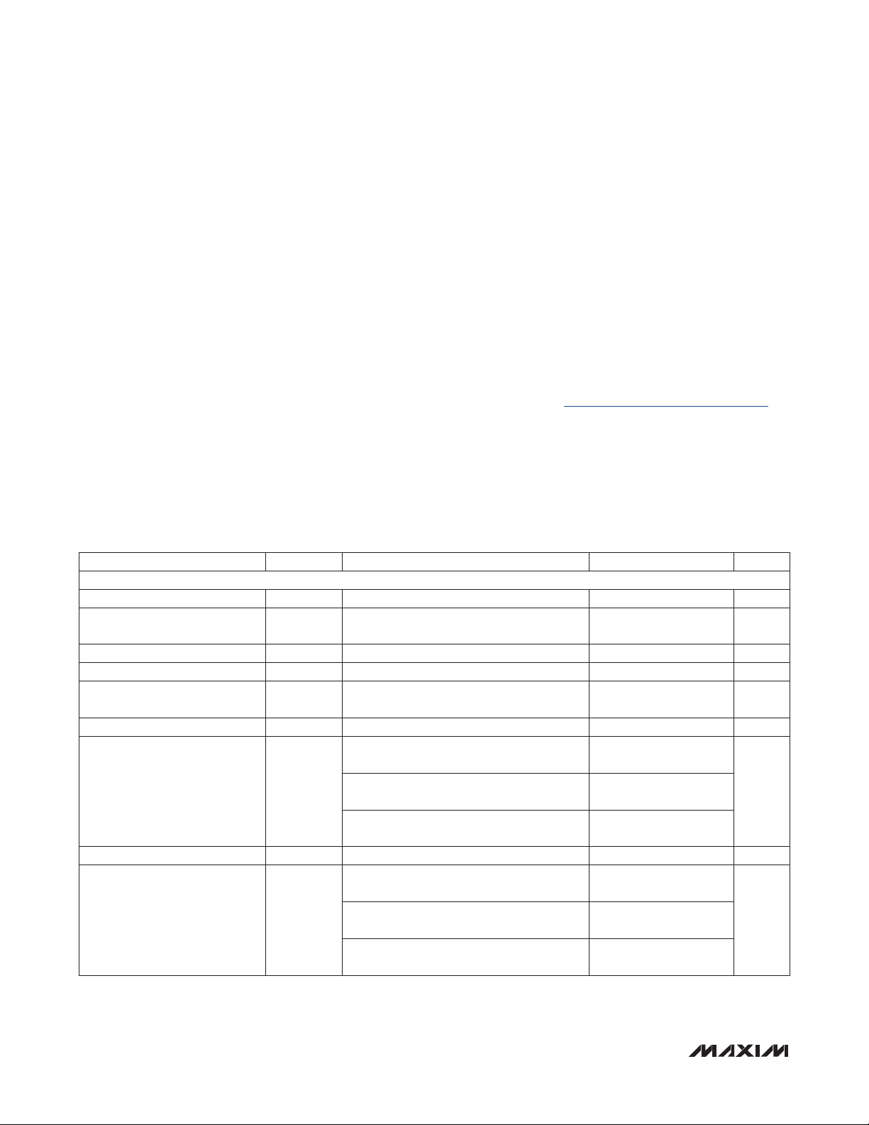
ELECTRICAL CHARACTERISTICS
MAX14805/MAX14806
(VDD = +2.7V to +5.5V, VPP = +40V to (VNN + 200V), VNN = -40V to -160V, TA = T
values are at TA = +25NC.) (Note 2)
PARAMETER SYMBOL CONDITIONS MIN TYP MAX UNITS
POWER SUPPLIES
V
Supply Voltage V
DD
VPP Supply Voltage V
VNN Supply Voltage V
V
Supply Quiescent Current I
DD
V
Supply Dynamic Current I
DD
V
Supply Quiescent Current I
PP
V
Supply Dynamic Current
PP
(All Channel Switching
Simultaneously)
DD
PP
NN
DDQ
DDD
PPQ
I
PP
VDD = +5V, LE = GND, f
5MHz
V
= +40V, VNN = -160V, f
PP
f
= f
DIN1
DIN2
V
= +100V, VNN = -100V, f
PP
f
= f
DIN1
DIN2
VPP = +160V, VNN = -40V, f
f
= f
DIN1
DIN2
V
Supply Quiescent Current I
NN
V
Supply Dynamic Current
NN
(All Channel Switching
Simultaneously)
NNQ
I
NN
V
= +40V, VNN = -160V, f
PP
f
= f
DIN1
DIN2
V
= +100V, VNN = -100V, f
PP
f
= f
DIN1
DIN2
VPP = +160V, VNN = -40V, f
f
= f
DIN1
DIN2
Junction-to-Ambient Thermal Resistance
BJA (Note 1) .................................................................44NC/W
Junction-to-Ambient Thermal Resistance
BJC (Note 1) ................................................................10NC/W
Operating Temperature Range .......................... -40NC to +85NC
Storage Temperature Range ............................ -65NC to +150NC
Junction Temperature ................................................... +150NC
Lead Temperature (soldering, 10s) ................................+300NC
Soldering Temperature (reflow) ......................................+260NC
MIN
to T
, unless otherwise noted. Typical
MAX
2.7 5.5 V
V
40 100
NN
+ 220
-160 -100 -15 V
5
= f
DIN2
=
2 mA
DIN1
10
= 50kHz,
SW_
= 50kHz, LE = GND
SW_
= 50kHz, LE = GND
SW_
= 50kHz, LE = GND
= 50kHz,
= 50kHz,
5
6
7
10
= 50kHz,
SW_
= 50kHz, LE = GND
SW_
= 50kHz, LE = GND
SW_
= 50kHz, LE = GND
= 50kHz,
= 50kHz,
5.5
5
4.5
V
FA
FA
mA
FA
mA
2 ______________________________________________________________________________________
Page 3
16-Channel (Two Banks of 8-Channel),
High-Voltage Analog Switches
ELECTRICAL CHARACTERISTICS (continued)
(VDD = +2.7V to +5.5V, VPP = +40V to (VNN + 200V), VNN = -40V to -160V, TA = T
values are at TA = +25NC.) (Note 2)
PARAMETER SYMBOL CONDITIONS MIN TYP MAX UNITS
SWITCH CHARACTERISTICS
Analog Signal Range V
Small-Signal
On-Resistance
Small-Signal
On-Resistance Matching
DR
Large-Signal Switch
On-Resistance
Shunt Resistance R
Switch-Off Leakage I
SW_(OFF)
Switch-Off DC Offset
R
R
SW_
ONS
ONS
ONL
INT
(Note 3) V
V
= +40V,
PP
V
= -160V,
NN
V
= 0V
SW_
V
= +100V,
PP
V
= -100V,
NN
V
= 0V
SW_
V
= +160V,
PP
V
= -40V,
NN
V
= 0V
SW_
VPP = +100V, VNN = -100V, I
V
= V
SW_
PP
- 10V, I
I
= 5mA 28 52
SW
I
= 200mA 22 37
SW
I
= 5mA 22 34
SW
I
= 200mA 18 27
SW
I
= 5mA 20 30
SW
I
= 200mA 16 23
SW
SW_
= 1A 15
SW_
MAX14806 only 27 40 53
V
= VPP - 10V or unconnected
SW_
(MAX14805 only) (Figure 1)
RL = 100kI (Figure 1)
Switch Output Peak Current 100ns pulse width, 0.1% duty cycle 3 A
Switch Output Isolation Diode
Current
300ns pulse width, 2% duty cycle
(Figure 1)
SWITCH DYNAMIC CHARACTERISTICS
V
= V
Turn-On Time t
Turn-Off Time t
Output Switching Frequency f
Off-Isolation V
Crosstalk V
Switch Off-Capacitance
(Note 4)
Switch On-Capacitance
(Note 4)
C
SW_(OFF)VSW_
C
SW_ (ON)VSW_
Output Voltage Spike (Note 4) V
Small-Signal Analog Bandwidth f
ON
OFF
SW
ISO
CT
SPK
BW
SW_
VNN = -40V to -160V (Figure 1)
V
SW_
VNN = -40V to -160V (Figure 1)
Duty cycle = 50% 50 kHz
f = 5MHz, RL = 1kI, CL = 15pF (Figure 1)
f = 5MHz, RL = 50I (Figure 1)
f = 5MHz, RL = 50I (Figure 1)
RL = 50I (Figure 1)
V
= +100V, V
PP
- 10V, RL = 10kI,
PP
= V
- 10V, RL = 10kI,
PP
= 0V, f = 1MHz 4 11 18 pF
= 0V, f = 1MHz 20 36 56 pF
= -100V, CL = 200pF 20 MHz
NN
MIN
to T
, unless otherwise noted. Typical
MAX
V
-
NN
PP
10
= 5mA 5 %
0 2.5
-30 +30 mV
2 A
5
5
-50
-77
-80 dB
-500 +250 mV
MAX14805/MAX14806
V
I
I
kI
FA
Fs
Fs
dB
_______________________________________________________________________________________ 3
Page 4
16-Channel (Two Banks of 8-Channel),
High-Voltage Analog Switches
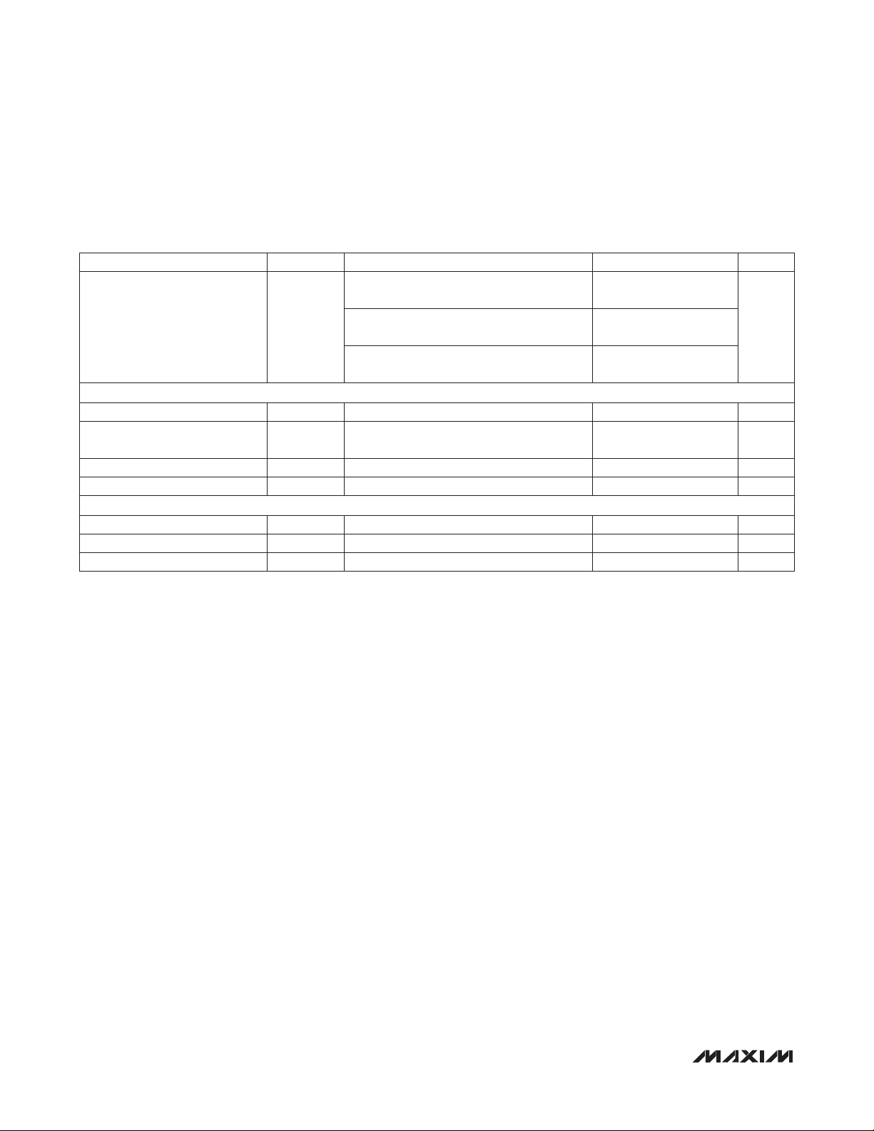
ELECTRICAL CHARACTERISTICS (continued)
(VDD = +2.7V to +5.5V, VPP = +40V to (VNN + 200V), VNN = -40V to -160V, TA = T
values are at TA = +25NC.) (Note 2)
PARAMETER SYMBOL CONDITIONS MIN TYP MAX UNITS
V
= +40V, V
PP
(Figure 1)
V
= +100V, V
Charge Injection Q
LOGIC LEVELS (DIN1, DIN2, LE)
Logic-Input Low Voltage V
Logic-Input High Voltage V
Logic-Input Capacitance C
Logic-Input Leakage Current I
LOGIC TIMING (See Timing Diagram, Figure 2)
MAX14805/MAX14806
Setup Time t
Hold Time t
Time Width of LE
Note 2: All devices are 100% tested at TA = +85NC. Limits over the operating temperature range are guaranteed by design and
characterization.
Note 3: The analog signal input V
Note 4: Guaranteed by characterization; not production tested.
IL
IH
IN
IN
SD
HOLD
t
WLE
must satisfy VNN P V
SW_
PP
(Figure 1)
V
= +160V, V
PP
(Figure 1)
SW_
= -160V, V
NN
= -100V, V
NN
= -40V, V
NN
P VPP or remain unconnected during power-up.
SW_
SW_
SW_
MIN
= 0V
= 0V
= 0V
to T
, unless otherwise noted. Typical
MAX
650
450
250
0.75 V
VDD -
0.75
10 pF
-1 +1
30 ns
30 ns
30 ns
pC
V
FA
4 ______________________________________________________________________________________
Page 5
VPP - 10V
V
+ 10V
NN
16-Channel (Two Banks of 8-Channel),
High-Voltage Analog Switches
MAX14805/MAX14806
V
- 10V
PP
R
L
100k
I
SOL
SW_
SW_
V
OUT
R
100k
MAX14805
MAX14806
V
V
V
PP
NN
PP
V
NN
V
GND
DD
V
5V
V
SW_
SW_
L
Ω
MAX14805
MAX14806
V
PP
NN
PP
V
NN
V
GND
DD
5V
Ω
V
OUT
SW_
SW_
MAX14805
MAX14806
V
V
V
PP
NN
PP
V
NN
V
GND
5V
DD
V
V
OUT
= 10V
OUT
AT 5MHz
R
L
V
V
SWITCH-OFF LEAKAGE
P-P
SW_
SW_
V
OUT
SW_
SW_
MAX14805
MAX14806
V
PP
NN
PP
V
NN
= 20LOG
V
ISO
OFF-ISOLATION
V
OUT
V
OUT
V
GND
V
OUT
V
IN
5V
DD
V
PP
V
NN
SW_
1000pF
SW_
V
SW_
MAX14805
MAX14806
V
V
V
PP
NN
PP
V
NN
DC OFFSET OFF
I
ID
V
NN
MAX14805
MAX14806
V
NN
V
PP
V
NN
ISOLATION DIODE CURRENT
+V
SPK
-V
V
V
DD
DD
GND
SPK
V
= 10V
OUT
AT 5MHz
50
Ω
V
SW_
SW_
PP
V
NN
MAX14805
V
DD
5V
GND
V
OUT
50
Ω
R
L
1k
Ω
MAX14806
V
V
V
PP
NN
PP
V
NN
tON/t
TEST CIRCUIT
OFF
P-P
SW_
SW_
SW_
SW_
50
Ω
MAX14805
MAX14806
V
PP
V
NN
= 20LOG
V
CT
CROSSTALK
V
DD
V
GND
V
OUT
V
IN
5V
5V
DD
GND
Figure 1. Test Circuits
_______________________________________________________________________________________ 5
Q = 1000pF x V
OUT
CHARGE INJECTION
OUTPUTVOLTAGE SPIKE
Page 6

16-Channel (Two Banks of 8-Channel),
High-Voltage Analog Switches
Typical Operating Characteristics
(VDD = +3V, VPP = +100V, VNN = -100V, TA = +25NC, unless otherwise noted.)
ON-RESISTANCE
vs. ANALOG SIGNAL VOLTAGE
MAX14805/6 toc01
ON-RESISTANCE (Ω)
120
VPP = +100V, VNN = -100V
100
80
60
40
20
0
-100 100
100
90
80
70
VPP = +100V, VNN = -100V
60
VPP = +40V, VNN = -960V
50
40
ON-RESISTANCE (Ω)
30
20
10
0
-150 150
VPP = +160V, VNN = -40V
VSW (V)
100500-50-100
MAX14805/MAX14806
OFF-ISOLATION vs. FREQUENCY
0
-20
-40
OFF-ISOLATION (dB)
TA = +85°C
-60
-80
0.001 100
TA = +25°C
TA = -40°C
FREQUENCY (MHz)
MAX14805/6 toc04
1010.10.01
LEAKAGE CURRENT vs. TEMPERATURE
80
60
40
I
COM_(OFF)(VCOM
LEAKAGE CURRENT (nA)
20
0
-40 85
ON-RESISTANCE
vs. ANALOG SIGNAL VOLTAGE
TA = +85°C
TA = +25°C
TA = -40°C
500-50
VSW (V)
= 0V)
I
COM_(ON)(VCOM
TEMPERATURE (°C)
I
COM_(OFF)(VCOM
I
COM_(ON)(VCOM
I
COM_(ON)(VCOM
= 0V)
I
COM_(OFF)(VCOM
= -90V)
= -90V)
= +90V)
= +90V)
603510-15
5
MAX14805/6 toc02
MAX14805/6 toc05
4
3
2
TURN-ON/TURN-OFF TIME (µs)
1
0
-90 90
1.2
1.0
0.8
0.6
SUPPLY CURRENT (µA)
0.4
DDQ
I
0.2
0
2.7 5.5
TURN-ON/TURN-OFF TIME
vs. ANALOG SIGNAL VOLTAGE
t
OFF
t
ON
60300-30-60
VNO (V)
LOGIC SUPPLY CURRENT
vs. SUPPLY VOLTAGE
TA = +25°C
TA = +85°C
TA = -40°C
VDD SUPPLY VOLTAGE (V)
MAX14805/6 toc03
MAX14805/6 toc06
5.14.74.33.93.53.1
HIGH-VOLTAGE SUPPLY CURRENT
vs. TEMPERATURE
0.20
VPP = +100V
= -100V
V
NN
0.15
0.10
SUPPLY CURRENT (µA)
0.05
0
-40 85
TEMPERATURE (°C)
I
MAX14805/6 toc07
I
PP
NN
603510-15
HIGH-VOLTAGE SUPPLY CURRENT
vs. SWITCHING FREQUENCY
8
ALL SWITCHES SWITCHING
= +25°C
T
A
6
4
SUPPLY CURRENT (mA)
2
0
0 50
DIN_ SWITCHING FREQUENCY (kHz)
I
PP
I
NN
40302010
6 ______________________________________________________________________________________
MAX14805/6 toc08
Page 7

16-Channel (Two Banks of 8-Channel),
High-Voltage Analog Switches
Pin Configuration
SW5
SW5
SW6
SW6
SW7
SW7
SW8
SW8
SW9
SW9
SW10
SW10
TOP VIEW
3635343332313029282726
25
MAX14805/MAX14806
SW4
N.C.
SW4
N.C.
SW3
SW3
SW2
SW2
SW1
SW1
SW0
SW0
37
38
39
40
41
42
43
44
45
46
47
48
MAX14805
MAX14806
24
23
22
21
20
19
18
17
16
15
14
13
N.C.
SW11
SW11
SW12
SW12
SW13
SW13
SW14
SW14
SW15
SW15
N.C.
+
1
2
3
4
5
6
7
8
9
101112
PP
NN
V
V
N.C.
N.C.
DIN1LEDIN2
N.C.
N.C.
DD
V
N.C.
GND
TQFP
(7mm × 7mm × 1.4mm)
Pin Description
PIN NAME FUNCTION
1 V
2, 4, 8, 9, 12,
13, 24, 38, 40
3 V
NN
N.C. No Connection. Not internally connected.
PP
Negative High-Voltage Power Supply. Bypass VNN to GND with a 0.1FF or greater ceramic
capacitor as close as possible to the device.
Positive High-Voltage Power Supply. Bypass VPP to GND with a 0.1FF or greater ceramic capacitor as close as possible to the device.
5 DIN1 Data Input 1
6
LE Active-Low Latch Enable Input. Drive LE low to latch data input. Drive LE high to hold data.
7 DIN2 Data Input 2
10 V
DD
Digital Power Supply. Bypass VDD to GND with a 0.1FF or greater ceramic capacitor as close as
possible to the device.
11 GND Ground
14, 15 SW15 Analog Switch Terminal 15
_______________________________________________________________________________________ 7
Page 8

16-Channel (Two Banks of 8-Channel),
High-Voltage Analog Switches
Pin Description (continued)
PIN NAME FUNCTION
16, 17 SW14 Analog Switch Terminal 14
18, 19 SW13 Analog Switch Terminal 13
20, 21 SW12 Analog Switch Terminal 12
22, 23 SW11 Analog Switch Terminal 11
25, 26 SW10 Analog Switch Terminal 10
27, 28 SW9 Analog Switch Terminal 9
29, 30 SW8 Analog Switch Terminal 8
31, 32 SW7 Analog Switch Terminal 7
33, 34 SW6 Analog Switch Terminal 6
35, 36 SW5 Analog Switch Terminal 5
37, 39 SW4 Analog Switch Terminal 4
41, 42 SW3 Analog Switch Terminal 3
43, 44 SW2 Analog Switch Terminal 2
45, 46 SW1 Analog Switch Terminal 1
MAX14805/MAX14806
47, 48 SW0 Analog Switch Terminal 0
8 ______________________________________________________________________________________
Page 9

16-Channel (Two Banks of 8-Channel),
High-Voltage Analog Switches
MAX14805/MAX14806
V
DD
LE
0V
V
DD
DIN_
0V
ON
SW_
OFF
Figure 2. Digital Control (DIN1/DIN2/LE) Timing
50%
t
t
SD
HOLD
50%
50%
50% 50%
t
ON
t
WLE
50% 50%
t
OFF
Table 1. Truth Table
CONTROL ANALOG SWITCH
DIN1 DIN2
LE
Low Low Low Off Off
High Low Low On Off
Low High Low Off On
High High Low On On
X X High Hold Previous State
X = Don’t care.
_______________________________________________________________________________________ 9
SW0–SW7 SW8–SW15
Page 10

16-Channel (Two Banks of 8-Channel),
High-Voltage Analog Switches
Detailed Description
The MAX14805/MAX14806 provide high-voltage switching on 16 channels for ultrasonic imaging. Both devices
are ideal for the following applications: bank selection in
biplane or triplane ultrasound probes and relays replacement in medical ultrasound systems. The devices utilize
200V process technology to provide 16 high-voltage,
low-charge injection SPST switches, controlled by a
digital interface.
The MAX14805/MAX14806’s output switches are configured as two sets of eight SPST analog switches. The
switches are controlled by two input logic controls, DIN1
and DIN2 (respectively for switch 0 to 7 and switch 8
to 15). The MAX14806 features integrated 40kI bleed
resistors on each switch terminal that help to reduce
voltage buildup in capacitive loads such as piezoelectric
elements.
The MAX14805/MAX14806 operate with a wide range of
MAX14805/MAX14806
high-voltage supplies, including VPP/VNN = +100V/-100V,
+200V/0V and +40V/-160V. The digital interface operates from a separate VDD supply from +2.7V to +5.5V.
Digital inputs DIN1, DIN2, and LE operate on the VDD
supply voltage.
The MAX14805CCM+ is a drop-in replacement for the
Supertex HV2631. The MAX14806CCM+ is a drop-in
replacement for the Supertex HV2731.
Analog Switch
The MAX14805/MAX14806 allow a peak-to-peak analog
signal range from VNN to (V
and power-down, all analog switch inputs (SW_) must be
unconnected or satisfy VNN P V
- 10V). During power-up
PP
P VPP.
SW_
High-Voltage Supplies
The MAX14805/MAX14806 allow a wide range of highvoltage supplies. The devices operate with VNN from
-160V to 0V and VPP from +40V to (VNN + 220V). When
VNN is connected to GND (single-supply applications),
the devices operate with VPP up to +200V. The VPP and
VNN high-voltage supplies are not required to be symmetrical, but the voltage difference (VPP - VNN) must not
exceed 230V.
Bleed Resistors (MAX14806)
The MAX14806 features integrated 40kI bleed resistors to discharge capacitive loads such as piezoelectric
transducers. Each analog switch terminal is connected
to GND with a bleed resistor.
Data Input (DIN1/DIN2)
DIN1/DIN2 control the on/off state of the analog switches.
DIN1 controls SW0–SW7 and DIN2 controls SW8–SW15
(see Table 1 and Figure 2). DIN1 and DIN2 operate on
the VDD supply voltage.
Latch Enable (LE)
Drive LE logic-low to latch DIN1/DIN2 data input (see
Figure 2). Drive LE logic-high to hold data. The LE input
operates on the VDD supply voltage.
Applications Information
For medical ultrasound applications, see Figures 3 and 4.
Supply Sequencing and Bypassing
The MAX14805/MAX14806 do not require special
sequencing of the VDD, VPP, and VNN supply voltages;
however, analog switch inputs must be unconnected or
satisfy VNN P V
down. Bypass VDD, VPP, and VNN to GND with a 0.1FF
ceramic capacitor as close as possible to the device.
P VPP during power-up and power-
SW_
10 _____________________________________________________________________________________
Page 11

16-Channel (Two Banks of 8-Channel),
High-Voltage Analog Switches
Application Diagram
MAX14805/MAX14806
HIGH-VOLTAGE TRANSMIT
1 PER CHANNEL
±100V MAX
LOW-VOLTAGE RECEIVE
64 TO 128 CHANNELS
±1V MAX
+V
-V
MAINFRAME
10mA TYP
HIGH-VOLTAGE
ISOLATION
PROBE SELECTION
2 TO 4 PROBES
MAX14805
MAX14806
PROBE
A
CABLE
1 PER CHANNEL
±1A TO ±2A MAX
PROBES
TRANSDUCERS
Figure 3. Relay Replacement Application in Medical System
______________________________________________________________________________________ 11
PROBE
B
Page 12

16-Channel (Two Banks of 8-Channel),
High-Voltage Analog Switches
Application Diagram (continued)
MAINFRAME
HIGH-VOLTAGE TRANSMIT
1 PER CHANNEL
±100V MAX
+V
10mA TYP
LOW-VOLTAGE RECEIVE
64 TO 128 CHANNELS
MAX14805/MAX14806
±1V MAX
HIGH-VOLTAGE
ISOLATION
-V
PROBE SELECTION
1 RELAY/CH/PROBE
Figure 4. Probe Banks Selection in Biplane or Triplane Probe
2 TO 4 PROBES
RELAY
PROBE
A
PROBE
B
PROBE
C
PROBE
D
CABLE
1 PER CHANNEL
±1A TO ±2A MAX
PROBES
MAX14805
MAX14806
TRANSDUCERS
TWO BANKS OF
ELEMENTS
BANK 1
128 OR MORE
ELEMENTS
BANK 2
128 OR MORE
ELEMENTS
12 _____________________________________________________________________________________
Page 13

16-Channel (Two Banks of 8-Channel),
High-Voltage Analog Switches
Functional Diagram
MAX14805/MAX14806
DIN1
DIN2
V
DD
LE
V
DD
LATCH
GND
V
PP
LEVEL
SHIFTER 1
V
NN
V
PP
SW0
*
V
NN
SW1
*
V
NN
SW7
*
V
NN
SW7
*
V
DD
LATCH
GND
V
PP
LEVEL
SHIFTER 2
V
NN
GND
*
*
V
NN
SW8
V
NN
SW8
V
NN
MAX14805
MAX14806
GND
*BLEED RESISTORS AVAILABLE ON THE MAX14806 ONLY.
Chip Information
PROCESS: BiCMOS
______________________________________________________________________________________ 13
SW15
*
V
NN
SW15
*
V
NN
V
NN
Package Information
For the latest package outline information and land patterns,
go to www.maxim-ic.com/packages. Note that a “+”, “#”, or
“-“ in the package code indicates RoHS status only. Package
drawings may show a different suffix character, but the drawing
pertains to the package regardless of RoHS status.
PACKAGE TYPE PACKAGE CODE DOCUMENT NO.
48 TQFP C48-6
21-0054
Page 14

16-Channel (Two Banks of 8-Channel),
High-Voltage Analog Switches
Revision History
REVISION
NUMBER
0 4/10 Initial release —
REVISION
DATE
MAX14805/MAX14806
DESCRIPTION
PAGES
CHANGED
Maxim cannot assume responsibility for use of any circuitry other than circuitry entirely embodied in a Maxim product. No circuit patent licenses are implied.
Maxim reserves the right to change the circuitry and specifications without notice at any time.
14 Maxim Integrated Products, 120 San Gabriel Drive, Sunnyvale, CA 94086 408-737-7600
©
2010 Maxim Integrated Products Maxim is a registered trademark of Maxim Integrated Products, Inc.
 Loading...