

Page 1
19-4503; Rev 0; 4/09
3-Channel, Low-Leakage ESD Protector
General Description
The MAX14541E low-capacitance Q15kV ESD-protection
diode array is designed to protect sensitive electronics
attached to communication lines. Each channel consists
of a pair of diodes that steer ESD current pulses to VCC
or GND.
The MAX14541E protects against ESD pulses up to
Q15kV Human Body Model (HBM) and Q15kV Air-Gap
Discharge, as specified in IEC 61000-4-2. The device
has a 6pF (typ) on-capacitance per channel, making
them ideal for use on high-speed data I/O interfaces.
The MAX14541E is a triple I/O protector designed for
biometric connectors, portable connectors, and SVGA
video connections with ultra-low leakage current.
The device is available in a 5-pin SC70 package and is
specified over the -40NC to +125NC automotive operating
temperature range.
Applications
Glucose Meters
MP3 Players
Digital Cameras
Handheld Equipment
Features
S High-Speed Data Line ESD Protection
±15kV Human Body Model
±15kV IEC 61000-4-2 Air-Gap Discharge
±8kV IEC 61000-4-2 Contact Discharge
S 6pF (typ) Low Input Capacitance
S 1nA (max) Low-Leakage Current
S +0.9V to +16V Supply Voltage Range
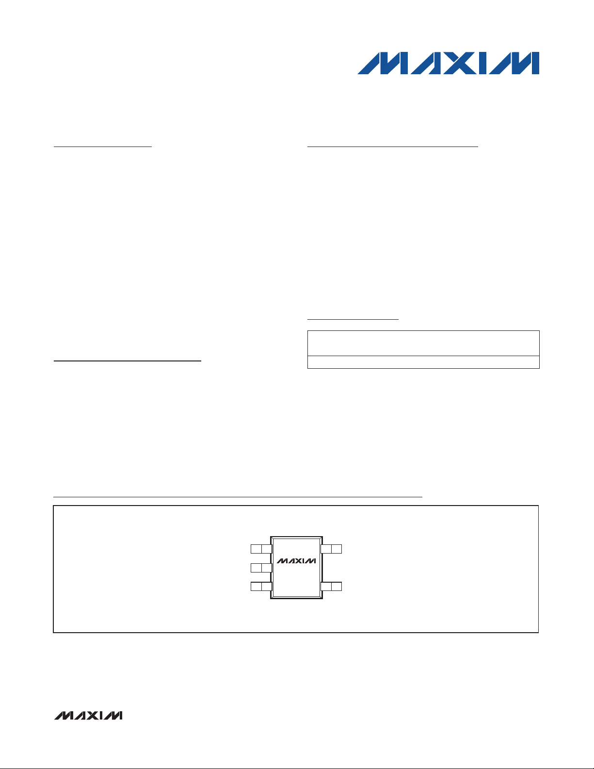
S 5-Pin SC70 (2.0mm x 2.2mm) Package
Ordering Information
PART
MAX14541EAXK+T -40NC to +125NC 5 SC70 ATY
+Denotes a lead(Pb)-free/RoHS-compliant package.
T = Tape and reel.
TEMP
RANGE
PIN-
PACKAGE
TOP
MARK
MAX14541E
Pin Configuration
TOP VIEW
1
2
3
+
MAX14541E
SC70
5
I/O-3
4
I/O-2
V
CC
GND
I/O-1
_______________________________________________________________ Maxim Integrated Products 1
For pricing, delivery, and ordering information, please contact Maxim Direct at 1-888-629-4642,
or visit Maxim’s website at www.maxim-ic.com.
Page 2
3-Channel, Low-Leakage ESD Protector
ABSOLUTE MAXIMUM RATINGS
(Voltages referenced to GND.)
VCC to GND ...........................................................-0.3V to +18V
I/O-1, I/O-2, I/O-3 to GND ........................ -0.3V to (VCC + 0.3V)
Continuous Power Dissipation (TA = +70NC)
5-Pin SC70 (derate 3.1mW/NC above +70NC) .........246.9mW
Thermal Resistance (Note 1)
BJA .............................................................................324NC/W
BJC ............................................................................115NC/W
Note 1: Package thermal resistances were obtained using the method described in JEDEC specification JESD51-7, using a four-
MAX14541E
Stresses beyond those listed under “Absolute Maximum Ratings” may cause permanent damage to the device. These are stress ratings only, and functional operation of the device at these
or any other conditions beyond those indicated in the operational sections of the specifications is not implied. Exposure to absolute maximum rating conditions for extended periods may
affect device reliability.
layer board. For detailed information on package thermal considerations, refer to www.maxim-ic.com/thermal-tutorial.
ELECTRICAL CHARACTERISTICS
(VCC = +5V, TA = T
PARAMETER SYMBOL CONDITIONS MIN TYP MAX UNITS
Supply Voltage V
Supply Current I
Diode Forward Voltage V
Channel Clamp Voltage
(Note 3)
Channel Leakage Current
(Note 4)
I/O Capacitance Bias of VCC/2, f = 1MHz (Note 4) 6 7 pF
ESD PROTECTION
Human Body Model ±15 kV
IEC 61000-4-2 Air-Gap
Discharge
IEC 61000-4-2 Contact
Discharge
Note 2: Parameters are 100% production tested at TA = +25°C. Specifications over temperature guaranteed by design only.
Note 3: Idealized clamp voltages. See the Applications Information section for more information.
Note 4: Guaranteed by design, not production tested.
MIN
to T
, unless otherwise noted. Typical values are at TA = +25NC.) (Note 2)
MAX
CC
CC
IF = 10mA, TA = +25°C 0.65 0.95 V
F
TA = +25°C, ±15kV
Human Body Model,
IF = 10A
TA = +25°C, ±8kV
Contact Discharge
V
(IEC 61000-4-2),
C
IF = 24A
TA = +25°C, ±15kV
Air-Gap Discharge
(IEC 61000-4-2),
IF = 45A
TA = -40°C to +50°C -1 +1 nA
TA = -40°C to +125°C -1 +1 µA
Operating Temperature Range ........................ -40NC to +125NC
Storage Temperature Range ............................ -65NC to +150NC
Junction Temperature .....................................................+150NC
Lead Temperature (soldering, 10s) ................................+300NC
0.9 16 V
1 100 nA
Positive transients
Negative transients -25
Positive transients
Negative transients -60
Positive transients
Negative transients -100 V
±15 kV
VCC +
25
VCC +
60
VCC +
100
±8 kV
V
V
V
2 ______________________________________________________________________________________
Page 3
3-Channel, Low-Leakage ESD Protector
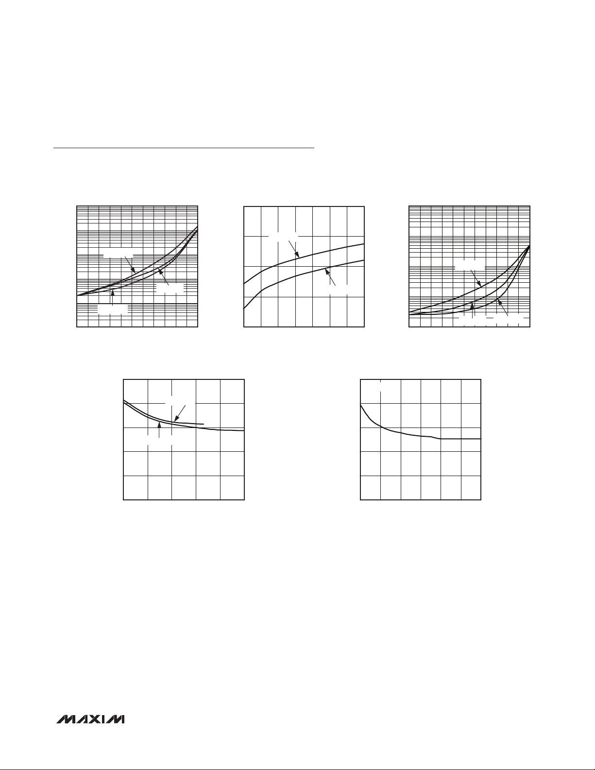
SUPPLY CURRENT
CLAMP VOLTAGE
I/O LEAKAGE CURRENT
INPUT CAPACITANCE
INPUT CAPACITANCE
Typical Operating Characteristics
(VCC = +5V, TA = +25NC, unless otherwise noted.)
MAX14541E
100
10
1
0.1
SUPPLY CURRENT (nA)
0.01
0.001
-40
VCC = 12V
VCC = 3.3V
INPUT CAPACITANCE (pF)
vs. TEMPERATURE
TEMPERATURE (oC)
vs. INPUT VOLTAGE
10
8
6
VCC = 5V
4
2
VCC = 5V
80 955 655020-25 35-10 125110
VCC = 3.3V
MAX14541E toc01
1.1
vs. DC CURRENT
1.0
0.9
CLAMP VOLTAGE (V)
0.8
0.7
10 90
I/O TO V
MAX14541E toc04
CC
I/O TO GND
7050 11030 130 150
DC CURRENT (mA)
10
MAX14541E toc02
0.1
I/O LEAKAGE CURRENT (nA)
0.01
0.001
vs. INPUT VOLTAGE
10
VCC = 12V
8
6
4
INPUT CAPACITANCE (pF)
2
vs. TEMPERATURE
1
VCC = 12V
VCC = 5V
-40
TEMPERATURE (oC)
VCC = 3.3V
80 955 655020-25 35-10 125110
MAX14541E toc05
MAX14541E toc03
0
0
21 43 5
INPUT VOLTAGE (V)
0
0
INPUT VOLTAGE (V)
8 1062 4 12
_______________________________________________________________________________________ 3
Page 4

3-Channel, Low-Leakage ESD Protector
_______________________________________________________________Pin Description
PIN NAME FUNCTION
1 V
2 GND Ground. Connect GND with a low-impedance connection to the ground plane.
3 I/O-1 ESD-Protected Channel
4 I/O-2 ESD-Protected Channel
5 I/O-3 ESD-Protected Channel
CC
Power-Supply Input. Bypass VCC to GND with a 0.1FF ceramic capacitor as close as possible to
the device.
MAX14541E
__________________________________________________________Functional Diagram
MAX14541E
V
CC
I/O-1 I/O-2
I/O-3
GND
4 ______________________________________________________________________________________
Page 5
3-Channel, Low-Leakage ESD Protector
( )
________________Detailed Description
The MAX14541E low-leakage, low-capacitance, Q15kV
ESD-protection diode arrays are suitable for high-speed
and general-signal ESD protection. Low input capacitance makes this device ideal for ESD protection of
high-speed signals. Each channel consists of a pair of
diodes that steer ESD current pulses to VCC or GND. The
MAX14541E is a 3-channel device (see the Functional
Diagram).
The MAX14541E is designed to work in conjunction with
a device’s intrinsic ESD protection. The MAX14541E
limits the excursion of the ESD event to below Q25V
peak voltage when subjected to the Human Body Model
waveform. When subjected to the IEC 61000-4-2 Contact
Discharge waveform, the peak voltage is limited to
Q60V. The peak voltage is limited to Q100V when subjected to Air-Gap Discharge. The device protected by
the MAX14541E must be able to withstand these peak
voltages, plus any additional voltage generated by the
parasitic of the board.
___________Applications Information
Design Considerations
Maximum protection against ESD damage results from
proper board layout (see the Layout Recommendations
section). A good layout reduces the parasitic series
inductance on the ground line, supply line, and protected signal lines. The MAX14541E ESD diodes clamp the
voltage on the protected lines during an ESD event and
shunt the current to GND or VCC. In an ideal circuit, the
clamping voltage (VC) is defined as the forward voltage
drop (VF) of the protection diode, plus any supply voltage present on the cathode.
For positive ESD pulses:
VC = VCC + V
For negative ESD pulses:
VC = -V
The effect of the parasitic series inductance on the lines
must also be considered (Figure 1).
For positive ESD pulses:
F
F
where I
is the ESD current pulse.
ESD
During an ESD event, the current pulse rises from zero
to peak value in nanoseconds (Figure 2). For example,
in a +15kV IEC 61000-4-7 Air-Gap Discharge ESD event,
the pulse current rises to approximately 45A in 1ns
(di/dt = 45 x 109). An inductance of only 10nH adds an
additional 450V to the clamp voltage, and represents
approximately 0.5in of board trace. Regardless of the
device’s specified diode clamp voltage, a poor layout
with parasitic inductance significantly increases the
effective clamp voltage at the protected signal line.
Minimize the effects of parasitic inductance by placing
the MAX14541E as close as possible to the connector
(or ESD contact point).
A low-ESR 0.1FF capacitor is required between VCC and
GND to get the maximum ESD protection possible. This
bypass capacitor absorbs the charge transferred by a
positive ESD event. Ideally, the supply rail (VCC) would
absorb the charge caused by a positive ESD strike
without changing its regulated value. All power supplies
have an effective output impedance on their positive
rails. If a power supply’s effective output impedance is
1I, then by using V = I x R, the clamping voltage of VC
increases by the equation VC = I
ESD
x R
. A +8kV IEC
OUT
61000-4-2 ESD event generates a current spike of 24A.
The clamping voltage increases by V
= 24A x 1I, or
C
VC = 24V. Again, a poor layout without proper bypassing
increases the clamping voltage. A ceramic chip capacitor mounted as close as possible to the MAX14541E
VCC pin is the best choice for this application. A bypass
capacitor should also be placed as close as possible to
the protected device.
POSITIVE SUPPLY RAIL
L2
D1
I/O_
D2
PROTECTED
LINE
L1
MAX14541E
d I
V V V L1 L2
= + + × + ×
C CC F(D1)
ESD
dt dt
For negative ESD pulses:
V V L1 L3
= − + × + ×
C F(D2)
_______________________________________________________________________________________ 5
d(I ) d(I )
ESD ESD
dt dt
d(I )
ESD
L3
GROUND RAIL
Figure 1. Parasitic Series Inductance
Page 6

3-Channel, Low-Leakage ESD Protector
standard is generally lower than that measured using the
I
100%
90%
PEAK
I
MAX14541E
tR = 0.7ns to 1ns
10%
30ns
t
60ns
Human Body Model. Figure 2 shows the current waveform for the Q8kV IEC 61000-4-2 Level 4, ESD Contact
Discharge test. The Air-Gap Discharge test involves
approaching the device with a charged probe. The
Contact Discharge method connects the probe to the
device before the probe is energized.
R
C
1MI
CHARGE-CURRENT-
LIMIT RESISTOR
R
D
1.5kI
DISCHARGE
RESISTANCE
Figure 2. IEC 61000-4-2 ESD Generator Current Waveform
ESD Protection
ESD protection can be tested in various ways. The
MAX14541E are characterized for protection to the following limits:
U Q15kV using the Human Body Model
U Q8kV using the Contact Discharge Method specified
in IEC 61000-4-2
U Q15kV using the IEC 61000-4-2 Air-Gap Discharge
Method
________________ESD Test Conditions
ESD performance depends on a number of conditions.
Contact Maxim for a reliability report that documents test
setup, methodology, and results.
Human Body Model
Figure 3 shows the Human Body Model, and Figure
4 shows the current waveform it generates when discharged into a low impedance. This model consists of a
100pF capacitor charged to the ESD voltage of interest
which is then discharged into the device through a 1.5kI
resistor.
IEC 61000-4-2
The IEC 61000-4-2 standard covers ESD testing and
performance of finished equipment. The MAX14541E
helps users design equipment that meets Level 4 of
IEC 61000-4-2. The main difference between tests done
using the Human Body Model and IEC 61000-4-2 Model
is higher peak current in IEC 61000-4-2. Because series
resistance is lower in the IEC 61000-4-2 ESD test model
(Figure 5), the ESD-withstand voltage measured to this
HIGH-
VOLTAGE
DC
SOURCE
100pF
STORAGE
C
s
CAPACITOR
Figure 3. Human Body ESD Test Model
PEAK-TO-PEAK RINGING
I
r
(NOT DRAWN TO SCALE)
AMPERES
IP 100%
90%
36.8%
10%
0
0
t
RL
TIME
t
DL
CURRENT WAVEFORM
Figure 4. Human Body Model Current Waveform
HIGH-
VOLTAGE
DC
SOURCE
R
C
50I to 100I
CHARGE-CURRENT-
LIMIT RESISTOR
C
s
150pF
R
D
330I
DISCHARGE
RESISTANCE
STORAGE
CAPACITOR
Figure 5. IEC 61000-4-2 ESD Test Model
DEVICE
UNDER
TEST
DEVICE
UNDER
TEST
6 ______________________________________________________________________________________
Page 7
3-Channel, Low-Leakage ESD Protector
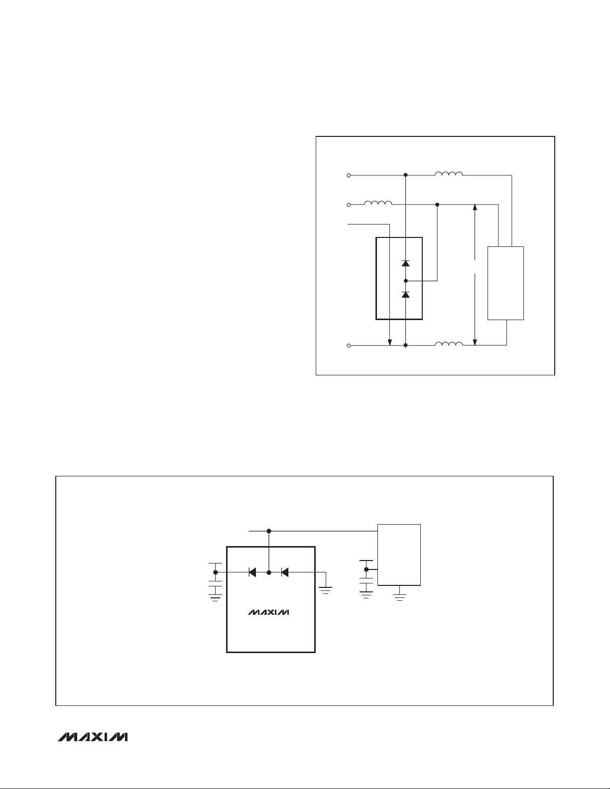
__________Layout Recommendations
Proper circuit-board layout is critical to suppress ESDinduced line transients (see Figure 6). The MAX14541E
clamps to 100V; however, with improper layout, the
voltage spike at the device can be much higher. A lead
inductance of 10nH with a 45A current spike results in an
additional 450V spike on the protected line. It is essential
that the layout of the PCB follows these guidelines:
1) Minimize trace length between the connector or input
terminal, I/O_, and the protected signal line.
2) Use separate planes for power and ground to reduce
parasitic inductance and to reduce the impedance to
the power rails for shunted ESD current.
3) Ensure short low-inductance ESD transient return
paths to GND and VCC.
4) Minimize conductive power and ground loops.
5) Do not place critical signals near the edge of the
PCB.
6) Bypass VCC to GND with a low-ESR ceramic capacitor as close as possible to VCC.
7) Bypass the supply of the protected device to GND
with a low-ESR ceramic capacitor as close as possible to the supply pin.
V
CC
L1
PROTECTED LINE
NEGATIVE ESD
CURRENT
PULSE
PATH TO
GROUND
GND
D1
I/O_
D2
Figure 6. Layout Considerations
MAX14541E
L2
V
C
PROTECTED
CIRCUIT
L3
___________________________________________________Typical Application Circuit
0.1µF
V
I/0
CC
PROTECTED
CIRCUIT
I/0 LINE
I/0_
V
CC
0.1µF
MAX14541E
_______________________________________________________________________________________ 7
Page 8

3-Channel, Low-Leakage ESD Protector
__________________________Chip Information
PROCESS: BiCMOS
MAX14541E
Package Information
For the latest package outline information and land patterns, go
to www.maxim-ic.com/packages.
PACKAGE TYPE PACKAGE CODE DOCUMENT NO.
5 SC70 X5+1
21-0076
Maxim cannot assume responsibility for use of any circuitry other than circuitry entirely embodied in a Maxim product. No circuit patent licenses are implied.
Maxim reserves the right to change the circuitry and specifications without notice at any time.
8 Maxim Integrated Products, 120 San Gabriel Drive, Sunnyvale, CA 94086 408-737-7600
©
2009 Maxim Integrated Products Maxim is a registered trademark of Maxim Integrated Products, Inc.
 Loading...