

Page 1
General Description
The MAX14527/MAX14528 overvoltage protection
devices feature a low 100mΩ (typ) RONinternal FET
and protect low-voltage systems against voltage faults
up to +28V. When the input voltage exceeds the overvoltage threshold, the internal FET is turned off to prevent damage to the protected components.
The overvoltage protection threshold can be adjusted
with optional external resistors to any voltage between
4V and 8V. With the OVLO input set below the external
OVLO select voltage, the MAX14527/MAX14528 automatically choose the internal ±2.5% accurate trip
thresholds. The internal overvoltage thresholds (OVLO)
are preset to 5.75V typical (MAX14527) or 6.76V typical
(MAX14528). The MAX14527/MAX14528 are also
protected against overcurrent events with an internal
thermal shutdown.
The MAX14527/MAX14528 are offered in a small, 8-pin
TDFN-EP package and operate over the -40°C to
+85°C extended temperature range.
Applications
Cell Phones
Media Players
PDAs and Palmtop Devices
Features
♦ Input Voltage Protection Up to +28V
♦ Preset Internal ±2.5% Accurate OVLO Thresholds
5.75V (MAX14527)
6.76V (MAX14528)
♦ Adjustable Overvoltage Protection Trip Level
♦ Integrated 100mΩ (typ) n-Channel MOSFET
Switch
♦ Soft-Start to Minimize In-Rush Current
♦ Automatic Overvoltage Protection Trip-Level
Selection
♦ Internal 15ms Startup Delay
♦ Thermal Shutdown Protection
♦ 8-Pin TDFN (2mm x 2mm) Package
♦ -40°C to +85°C Operating Temperature Range
MAX14527/MAX14528
Adjustable Overvoltage Protector
with High Accuracy
________________________________________________________________
Maxim Integrated Products
1
19-4357; Rev 0; 10/08
Ordering Information
PART
TOP
OVLO
(V)
MAX14527ETA+T
8 TDFN-EP* ACR 5.75
MAX14528ETA+T
8 TDFN-EP* ACS 6.76
For pricing, delivery, and ordering information, please contact Maxim Direct at 1-888-629-4642,
or visit Maxim's website at www.maxim-ic.com.
Note: Devices are specified over the -40°C to +85°C tempera-
ture range.
+
Denotes a lead-free/RoHS-compliant package.
T = Tape and reel.
*
EP = Exposed pad.
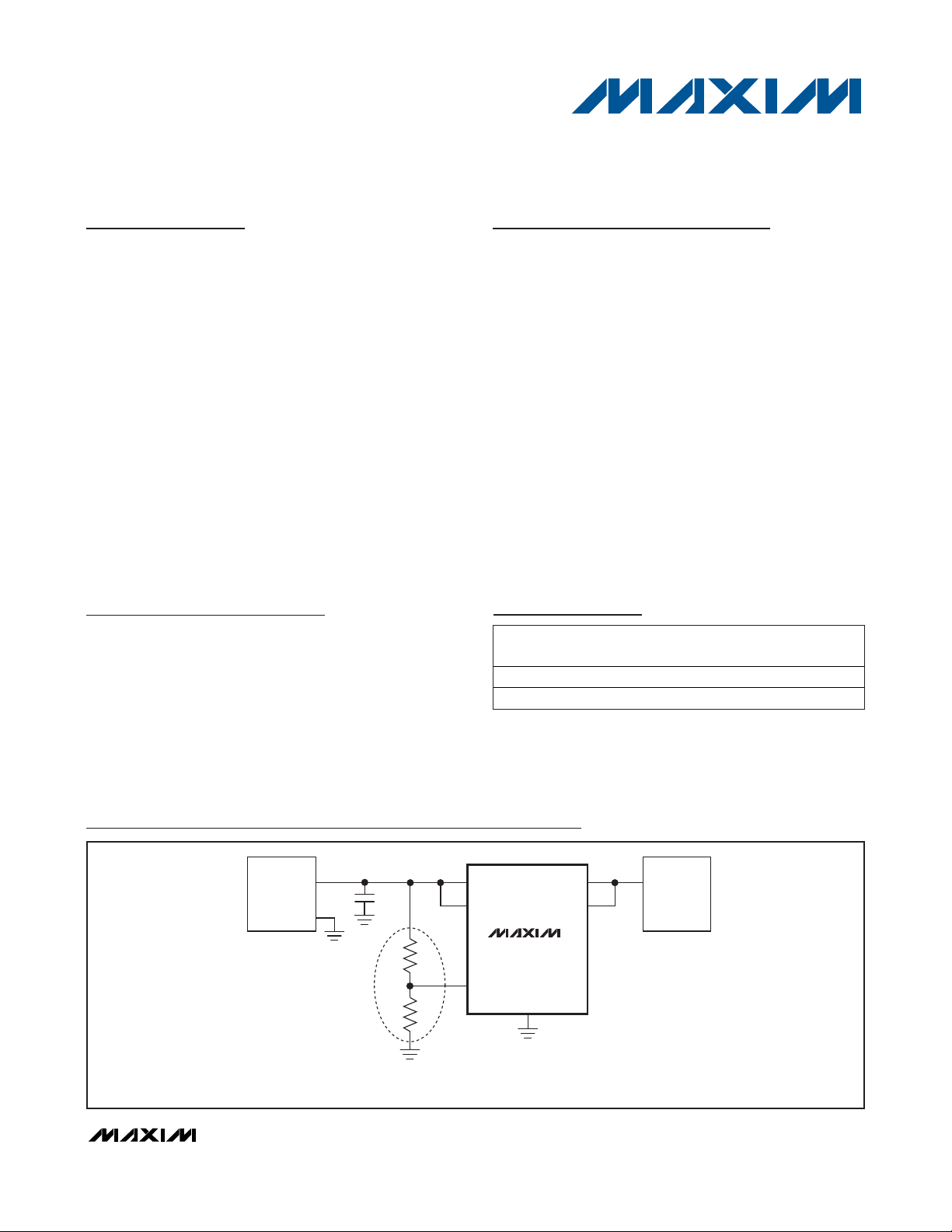
Typical Application Circuit
Pin Configuration appears at end of data sheet.
PIN-PACKAGE
MARK
USB
CONNECTOR
*R1 AND R2 ARE REQUIRED ONLY FOR ADJUSTABLE OVLO; OTHERWISE, CONNECT OVLO TO GND.
VBUS
1µF
IN
IN
R1
*
R2
MAX14527
MAX14528
OVLO
OUT
OUT
GND
CHARGER
INPUT
PMIC
Page 2

MAX14527/MAX14528
Adjustable Overvoltage Protector
with High Accuracy
2 _______________________________________________________________________________________
ABSOLUTE MAXIMUM RATINGS
Stresses beyond those listed under “Absolute Maximum Ratings” may cause permanent damage to the device. These are stress ratings only, and functional
operation of the device at these or any other conditions beyond those indicated in the operational sections of the specifications is not implied. Exposure to
absolute maximum rating conditions for extended periods may affect device reliability.
(All voltages referenced to GND.)
IN ............................................................................-0.3V to +30V
OUT .............................................................-0.3V to (V
IN
+ 0.3V)
OVLO........................................................................-0.3V to +6V
Continuous IN Current .............................................................1A
Peak IN Current (Note 1)..........................................................5A
Continuous OVLO Current ...................................................50µA
Continuous Power Dissipation (T
A
= +70°C)
8-Pin TDFN (derate 11.9mW/°C above +70°C) ...........954mW
Package Junction-to-Ambient Thermal Resistance (θ
JA
)
(Note 2) .....................................................................83.9°C/W
Package Junction-to-Case Thermal Resistance (θ
JC
)
(Note 2) ........................................................................37°C/W
Operating Temperature Range ...........................-40°C to +85°C
Junction Temperature......................................................+150°C
Storage Temperature Range .............................-65°C to +150°C
Lead Temperature (soldering) .........................................+300°C
ELECTRICAL CHARACTERISTICS
(VIN= +2.2V to +28V, TA= -40°C to +85°C, unless otherwise noted. Typical values are at VIN= +5.0V and TA= +25°C.) (Note 3)
PARAMETER SYMBOL CONDITIONS
UNITS
Input Voltage Range V
IN
2.2 28 V
Input Supply Current I
IN
VIN < OVLO 80
µA
MAX14527 5.6
5.9
VIN rising
MAX14528
7
MAX14527
IN Overvoltage Trip Level V
IN_OVLO
VIN falling
MAX14528 6.5
V
IN Overvoltage Lockout Hysteresis
1%
OVLO Set Threshold
1.2
V
Adjustable OVLO Threshold Range
48V
External OVLO Select Threshold
0.5 V
Switch On-Resistance R
ON
mΩ
OVLO Clamp I
CLAMP
= 10µA 3
5.5 V
OUT Capacitor C
OUT
µF
OVLO Input Leakage Current I
OVLO
V
OVLO_THRESH
= 1.245V
nA
Thermal Shutdown
°C
Thermal Shutdown Hysteresis 20 °C
TIMING CHARACTERISTICS (Figure 1)
Debounce Time t
INDBC
Time from 2.2V < VIN < V
IN_OVLO
to
V
OUT
= 10% of V
IN
15 ms
2.2V < VIN < V
IN_OVLO
, R
LOAD
= 100Ω,
C
LOAD
= 100µF; V
OUT
from 10% to
90% of V
IN
0.7
Switch Turn-On Time t
ON
2.2V < VIN < V
IN_OVLO
, R
LOAD
= 100Ω,
C
LOAD
= 1mF; V
OUT
from 10% to 90%
of V
IN
1.4
ms
Switch Turn-Off Time t
OFF
VIN > V
OVLO_THRESH
to V
OUT
= 80% of
V
IN_OVLO
; R
LOAD
= 1kΩ, VIN rising at
2V/100ns
1.3 3.5 µs
Note 1: Limited by thermal shutdown.
Note 2: Package thermal resistances were obtained using the method described in JEDEC specification JESD51-7, using a four-layer
board. For detailed information on package thermal considerations, refer to www.maxim-ic.com/thermal-tutorial
.
Note 3: All specifications are 100% production tested at T
A
= +25°C, unless otherwise noted. Specifications are over -40°C to +85°C
and are guaranteed by design.
MIN TYP MAX
5.75
6.55 6.765
5.54 5.84
V
IN_OVLO_HYS
V
OVLO_THRESH
V
OVLO_SELECT
1.245 1.29
0.15 0.33
100 200
4.56
-100 +100
150
160
6.95
1000
Page 3
MAX14527/MAX14528
Adjustable Overvoltage Protector
with High Accuracy
_______________________________________________________________________________________ 3
Timing Diagram
90%
10%
90%
10%
t
INDBC
t
INDBC
t
ON
t
OFF
t
ON
IN
OVLO
2.2V
OUT
NOTE: WAVEFORMS ARE NOT TO SCALE.
80% V
IN_OVLO
V
IN_OVLO
Figure 1. Timing Characteristics
Page 4

MAX14527/MAX14528
Adjustable Overvoltage Protector
with High Accuracy
4 _______________________________________________________________________________________
Typical Operating Characteristics
(TA= +25°C, unless otherwise noted.)
0.5
0.8
0.7
0.6
0.9
1.0
1.1
1.2
1.3
1.4
1.5
-40 10-15 35 60 85
NORMALIZED R
0N
vs. TEMPERATURE
MAX14527/8 toc02
TEMPERATURE (°C)
NORMALIZED R
ON
VIN = 3.6V
VIN = 5.0V
0.95
0.98
0.97
0.96
0.99
1.00
1.01
1.02
1.03
1.04
1.05
-40 10-15 35 60 85
NORMALIZED OVLO THRESHOLD
vs. TEMPERATURE
MAX14527/8 toc03
TEMPERATURE (°C)
NORMALIZED OVLO THRESHOLD
0.95
0.98
0.97
0.96
0.99
1.00
1.01
1.02
1.03
1.04
1.05
-40 10-15 35 60 85
NORMALIZED EXTERNAL OVLO SET
THRESHOLD vs. TEMPERATURE
MAX14527/8 toc04
TEMPERATURE (°C)
NORMALIZED EXTERNAL OVLO SET THRESHOLD
0.5
0.8
0.7
0.6
0.9
1.0
1.1
1.2
1.3
1.4
1.5
-40 10-15 35 60 85
NORMALIZED EXTERNAL OVLO SELECT
THRESHOLD vs. TEMPERATURE
MAX14527/8 toc05
TEMPERATURE (°C)
NORMALIZED EXTERNAL OVLO SELECT THRESHOLD
0.95
0.98
0.97
0.96
0.99
1.00
1.01
1.02
1.03
1.04
1.05
-40 10-15 35 60 85
NORMALIZED DEBOUNCE TIME
vs. TEMPERATURE
MAX14527/8 toc06
TEMPERATURE (°C)
NORMALIZED DEBOUNCE TIME
POWER-UP RESPONSE
MAX14527/8 toc07
10ms/div
V
IN
5V/div
V
OUT
5V/div
I
OUT
100mA/div
OVERVOLTAGE FAULT RESPONSE
MAX14527/8 toc08
1μs/div
V
IN
5V/div
V
OUT
5V/div
I
OUT
50mA/div
IN SUPPLY CURRENT
vs. IN VOLTAGE
90
80
70
60
50
40
30
IN SUPPLY CURRENT (µA)
20
10
0
0 7 14 21 28
TA = +25°C
TA = +85°C
TA = -40°C
IN VOLTAGE (V)
MAX14527/8 toc01
Page 5

Detailed Description
The MAX14527/MAX14528 overvoltage protection
devices feature a low RONinternal FET and protect lowvoltage systems against voltage faults up to +28V. If
the input voltage exceeds the overvoltage threshold,
the internal FET is turned off to prevent damage to the
protected components. The 15ms debounce time prevents false turn-on of the internal FET during startup.
Device Operation
The MAX14527/MAX14528 have timing logic that
controls the turn-on of the internal FET. If VIN<
V
OVLO_THRESH
, the internal charge pump is enabled.
The charge-pump startup, after a 15ms debounce
delay, turns on the internal FET (see the
Functional
Diagram
). At any time, if VINrises above V
OVLO_
THRESH
, OUT is disconnected from IN.
MAX14527/MAX14528
Adjustable Overvoltage Protector
with High Accuracy
_______________________________________________________________________________________ 5
Pin Description
Functional Diagram
OUT
OUT
IN
IN
OVLO
GND
CHARGE
PUMP
LOGIC
CONTROL
SEL
V
BG
REFERENCE
+
-
TEMPERATURE
FAULTS
MAX14527
MAX14528
PIN
FUNCTION
1, 2 IN
Voltage Input. Bypass IN with a 1µF ceramic capacitor as close as possible to the device to obtain ±15kV
Human Body Model (HBM) ESD protection. Connect all the IN pins together for proper operation. IN is
protected to ±2kV HBM when IN is not bypassed with a capacitor to GND.
3
External OVLO Adjustment. Connect OVLO to GND when using the internal threshold. Connect a resistordivider to OVLO to set a different OVLO threshold; this external resistor-divider is completely independent
from the internal threshold.
4, 5 I.C. Internally Connected. Do not connect. Leave I.C. unconnected.
6 GND Ground
7, 8 OUT Output Voltage. Output of internal switch. Connect all the OUT outputs together for proper operation.
—EP
Exposed Pad. Connect exposed pad to ground. For enhanced thermal dissipation, connect EP to a copper
area as large as possible. Do not use EP as a sole ground connection.
NAME
OVLO
Page 6

MAX14527/MAX14528
Internal Switch
The MAX14527/MAX14528 incorporate an internal FET
with a 100mΩ (typ) RON. The FET is internally driven by
a charge pump that generates a necessary gate voltage above IN. The internal FET is capable of passing
more than 5A inrush current.
Overvoltage Lockout (OVLO)
The MAX14527 has a 5.75V (typ) overvoltage threshold
(OVLO).The MAX14528 has a 6.76V (typ) OVLO
threshold.
Thermal-Shutdown Protection
The MAX14527/MAX14528 feature thermal shutdown
circuitry. The internal FET turns off when the junction
temperature exceeds +150°C (typ). The device exits
thermal shutdown after the junction temperature cools
by 20°C (typ).
Applications Information
IN Bypass Capacitor
For most applications, bypass IN to GND with a 1µF
ceramic capacitor as close as possible to the device to
enable ±15kV (HBM) ESD protection on IN. If ±15kV
(HBM) ESD is not required, there is no capacitor
required at IN. If the power source has significant
inductance due to long lead length, take care to prevent overshoots due to the LC tank circuit and provide
protection if necessary to prevent exceeding the +30V
absolute maximum rating on IN.
OUT Output Capacitor
The slow turn-on time provides a soft-start function that
allows the MAX14527/MAX14528 to charge an output
capacitor up to 1000µF.
External OVLO Adjustment Functionality
If OVLO is connected to ground, the internal OVLO
comparator uses the internally set OVLO value.
If an external resistor-divider is connected to OVLO
and V
OVLO
exceeds the OVLO select voltage,
V
OVLO_ SELECT
, the internal OVLO comparator reads
the IN fraction fixed by the external resistor divider. R1=
1MΩ is a good starting value for minimum current consumption. Since V
IN_OVLO
, V
OVLO_THRESH
, and R1are
known, R2can be calculated from the following formula:
This external resistor-divider is completely independent
from the internal resistor-divider.
ESD Test Conditions
ESD performance depends on a number of conditions.
The MAX14527/MAX14528 are specified for ±15kV
(HBM) typical ESD resistance on IN when IN is
bypassed to ground with a 1µF ceramic capacitor.
HBM ESD Protection
Figure 2a shows the Human Body Model, and Figure
2b shows the current waveform it generates when discharged into a low impedance. This model consists of a
100pF capacitor charged to the ESD voltage of interest,
which is then discharged into the device through a
1.5kΩ resistor.
VV
R
R
IN_OVLO OVLO_THRESH
1
2
=×+
⎡
⎣
⎢
⎤
⎦
⎥
1
Adjustable Overvoltage Protector
with High Accuracy
6 _______________________________________________________________________________________
CHARGE-CURRENT-
LIMIT RESISTOR
DISCHARGE
RESISTANCE
STORAGE
CAPACITOR
C
s
100pF
R
C
1M
Ω
R
D
1.5k
Ω
HIGH-
VOLTAGE
DC
SOURCE
DEVICE
UNDER
TEST
Figure 2a. Human Body ESD Test Model
Figure 2b. Human Body Current Waveform
IP 100%
90%
AMPERES
36.8%
10%
0
0
t
RL
I
R
TIME
t
DL
CURRENT WAVEFORM
PEAK-TO-PEAK RINGING
(NOT DRAWN TO SCALE)
Page 7

MAX14527/MAX14528
Adjustable Overvoltage Protector
with High Accuracy
Maxim cannot assume responsibility for use of any circuitry other than circuitry entirely embodied in a Maxim product. No circuit patent licenses are
implied. Maxim reserves the right to change the circuitry and specifications without notice at any time.
Maxim Integrated Products, 120 San Gabriel Drive, Sunnyvale, CA 94086 408-737-7600 _____________________
7
© 2008 Maxim Integrated Products is a registered trademark of Maxim Integrated Products, Inc.
1IN
4I.C.
2IN
3OVLO
8 OUT
5 I.C.
7 OUT
6 GND
MAX14527
MAX14528
TDFN
2mm x 2mm
TOP VIEW
*CONNECT EXPOSED PAD TO GND.
*EP
Pin Configuration
Chip Information
PROCESS: BiCMOS
PACKAGE TYPE PACKAGE CODE DOCUMENT NO.
8 TDFN-EP T822+2
21-0168
Package Information
For the latest package outline information and land patterns, go to www.maxim-ic.com/packages.
 Loading...