

Page 1
General Description
The MAX14525 features a low RON35mΩ (typ) load
switch with four unique enable inputs. The MAX14525
is ideal for disconnecting the lithium-ion (Li+) battery
from the loads in portable devices such as cell phones.
The MAX14525 operates from a +2.2V to +5.5V supply
voltage.
The MAX14525 features an extremely low 0.8µA (typ)
quiescent supply current to maximize battery life in
portable devices. It is enabled from four possible
inputs: external charger connection capable of high
voltage up to +28V, travel adapter (TA), on key (ON_K),
factory mode enable (JIG), and switch enable (S_EN).
The S_EN input is internally ANDed with the switched
battery connection (IN).
The MAX14525 is available in a small 8-pin, 2mm x
2mm TDFN package and operates over the -40°C to
+85°C extended temperature range.
Applications
Cell Phones
PDAs
GPS
UMPC Computers
Digital Cameras
Features
♦ Low 35mΩ (typ) RONLoad Switch
♦ Ultra Low, 0.8µA (typ) Supply Current
♦ Four Enable Inputs:
TA: +28V (max) Capable
ON_K: Accurate +3V Trigger Enable
JIG: Factory Mode Enable
S_EN: Logically ANDed with IN
♦ Space-Saving 8-Pin, 2mm x 2mm TDFN Package
♦ Controlled Turn-On to Limit dI/dt Pulses Due to
Lead Inductance
MAX14525
Battery Switch with Four Enable Inputs
________________________________________________________________
Maxim Integrated Products
1
Pin Configuration
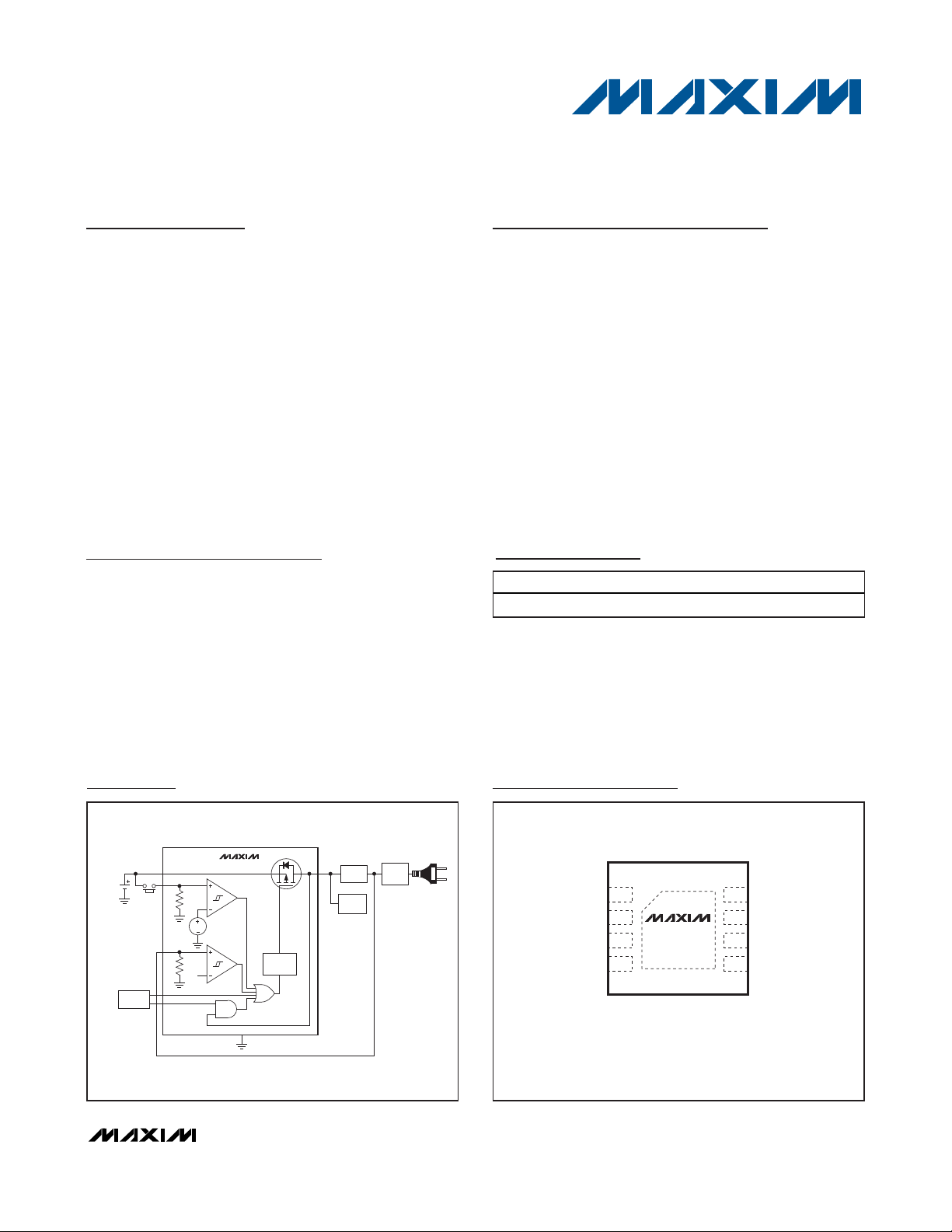
Typical Application Circuit
19-4356; Rev 0; 10/08
For pricing, delivery, and ordering information, please contact Maxim Direct at 1-888-629-4642,
or visit Maxim’s website at www.maxim-ic.com.
Ordering Information
PART PIN-PACKAGE TOP MARK
M AX 14525E TA+ T
8 TDFN-EP* ACQ
Note: The device is specified over the -40°C to +85°C operating
temperature range.
+
Denotes a lead-free/RoHS-compliant package.
*
EP = Exposed pad.
BAT
Li-ION
BATTERY
ON_K
ON
BUTTON
TA
JIG
P
S_EN
MAX14525
3.0V
SLEW RATE
2V
CONTROL
GND
TOP VIEW
IN
CHARGER
PHONE
LOADS
AC
ADAPTER
BAT
JIG
ON_K
S_EN
+
1
2
MAX14525
3
4
*EP
TDFN-EP
2mm x 2mm
*CONNECT EXPOSED PAD TO GND.
IN
8
IN
7
TA
6
GND
5
Page 2

MAX14525
Battery Switch with Four Enable Inputs
2 _______________________________________________________________________________________
ABSOLUTE MAXIMUM RATINGS
ELECTRICAL CHARACTERISTICS
(V
BAT
= +2.2V to +5.5V, TA= -40°C to +85°C, unless otherwise noted. Typical values are at V
BAT
= +3.6V and TA= +25°C.)
(Note 2)
Stresses beyond those listed under “Absolute Maximum Ratings” may cause permanent damage to the device. These are stress ratings only, and functional
operation of the device at these or any other conditions beyond those indicated in the operational sections of the specifications is not implied. Exposure to
absolute maximum rating conditions for extended periods may affect device reliability.
Note 1: Package thermal resistances were obtained using the method described in JEDEC specification JESD51-7, using a four-layer
board. For detailed information on package thermal considerations, refer to www.maxim-ic.com/thermal-tutorial
.
(All voltages referenced to GND.)
IN, BAT, JIG, S_EN, ON_K ................................... -0.3V to +6.0V
TA ...........................................................................-0.3V to +28V
Continuous Power Dissipation (T
A
= +70°C)
8-Pin TDFN (derate 11.9 mW/°C above +70°C) .........954 mW
Junction-to-Case Thermal Resistance
(θ
JC
) (Note 1) ...............................................................37°C/W
Junction-to-Ambient Thermal Resistance
(θ
JA
) (Note 1) ...............................................................84°C/W
Operating Temperature Range .......................... -40°C to +85°C
Junction Temperature..................................................... +150°C
Storage Temperature Range ............................ -65°C to +150°C
Lead Temperature (soldering, 10s) .................................+300°C
PARAMETER
CONDITIONS
DC CHARACTERISTICS
Input Voltage Range
2.2 5.5 V
On-Resistance R
ON
I
LOAD
= 100mA, V
BAT
= +3.0V 35 90 mΩ
Disable Supply Current
V
BAT
= +5.5V
(V
JIG
= V
S_EN
= V
ON_K
= VTA = VIN = 0)
1µA
V
BAT
Supply Current I
BAT
V
JIG
= V
S_EN
= V
BAT
, V
ON_K
= VTA = 0 0.8 4.5 µA
Increase in Supply Current with
V
JIG/VS_EN
Voltage
ΔI
BAT
V
JIG
= V
S_EN
= VIH or V
IL
2µA
Increase in Supply Current with
V
ON_K
Voltage
ΔI
BAT
V
BAT
= V
ON_K
= +3.6V 4.5 µA
Peak Current I
LIM
V
BAT
= +3.6V 5 A
UVLO Undervoltage Lockout Ramping V
BAT
1.9 V
LOGIC INPUT
TA Threshold Voltage V
TA_TH
1.7 2.5 V
TA Threshold Hysteresis 1%
TA Input Resistance VTA = 1V 50
kΩ
JIG, S_EN Input Logic-High V
IH
1.4 V
JIG, S_EN Input Logic-Low V
IL
0.4 V
JIG, S_EN Input Leakage Current
I
IN
V
BAT
= +5.5V
nA
IN AND Gate Threshold Voltage V
IN_TH
0.3 x
0.6 x
V
ON_K Threshold Voltage
Low-to-high transition
(Figure 1)
3.0
V
ON_K Threshold Hysteresis 1%
SYMBOL
V
, V
BAT
IN
I
BAT_DIS
MIN TYP MAX UNITS
V
ON_K_TH
1.15
100 180
-200 +200
V
BAT
2.94
V
BAT
3.06
Page 3
MAX14525
Battery Switch with Four Enable Inputs
_______________________________________________________________________________________ 3
PARAMETER
CONDITIONS
ON_K Input Leakage Current I
ON_K
V
BAT
= V
ON_K
= +3.6V 3 µA
SWITCH DYNAMICS (RL = 20Ω, CL = 0.1µF) (Figure 2)
Turn-On Delay Time t
ONDLY
µs
Turn-On Rise Time
VIN 10% to 90% of V
BAT
µs
Turn-Off Delay Time
From any enable low to VIN = 90% of V
BAT
µs
Turn-Off Fall Time
VIN 90% to 10% of V
BAT
60
µs
ELECTRICAL CHARACTERISTICS (continued)
(V
BAT
= +2.2V to +5.5V, TA= -40°C to +85°C, unless otherwise noted. Typical values are at V
BAT
= +3.6V and TA= +25°C.)
(Note 2)
Note 2: Devices are tested at T
A
= +25°C. Specifications over temperature are guaranteed by design.
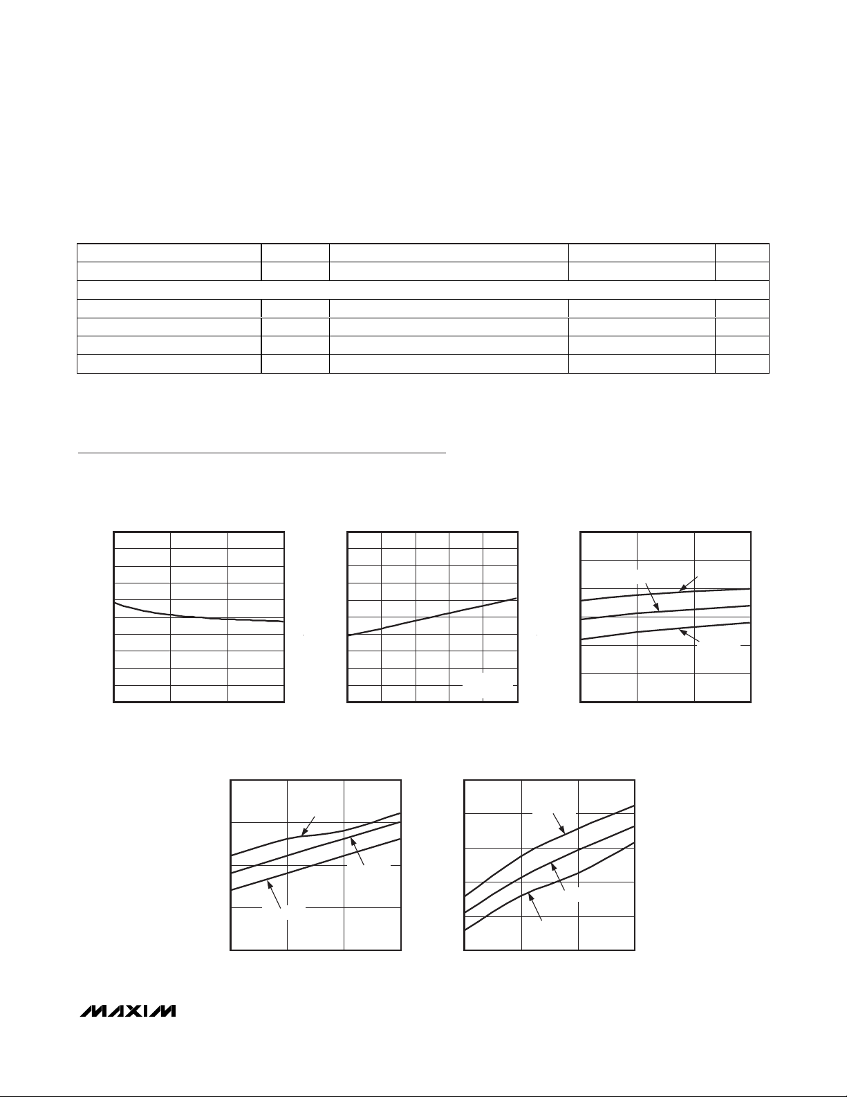
Typical Operating Characteristics
(VIN= +3.6V, TA= +25°C, unless otherwise noted.)
NORMALIZED RON vs. V
IN
MAX14525 toc01
VIN (V)
I
L
= 100mA
NORMALIZED R
ON
4.43.3
0.8
0.9
1.0
1.3
1.4
0.6
0.7
1.1
1.2
1.5
0.5
2.2 5.5
NORMALIZED RON vs. TEMPERATURE
MAX14525 toc02
TEMPERATURE (°C)
NORMALIZED R
ON
-15 60
0.6
0.8
1.0
1.6
1.8
0.4
1.4
0.2
1.2
2.0
0
-40 3510 85
IL = 100mA
V
BAT
= +3.0V
SYMBOL
From any enable high to VIN = 10% of V
t
ONRISE
t
OFFDLY
t
OFFFALL
BAT
MIN TYP MAX UNITS
600 2600
500 1800 5000
130 300
150
TA THRESHOLD vs. V
2.50
2.25
2.00
TA = +25°C
IN
TA = -40°C
MAX14525 toc03
3.010
ON_K THRESHOLD vs. V
3.005
3.000
ON_K THRESHOLD (V)
2.995
2.990
TA = -40°C
2.2 5.5
1.75
TA THRESHOLD (V)
1.50
1.25
1.00
2.2 5.5
IN
TA = +25°C
TA = +85°C
4.43.3
VIN (V)
1.25
MAX14525 toc04
1.15
1.05
0.95
S_EN THRESHOLD (V)
0.85
0.75
S_EN THRESHOLD vs. V
TA = -40°C
TA = +25°C
TA = +85°C
2.2 5.5
4.43.3
VIN (V)
TA = +85°C
4.43.3
VIN (V)
IN
MAX14525 toc05
Page 4

MAX14525
Battery Switch with Four Enable Inputs
4 _______________________________________________________________________________________
Typical Operating Characteristics (continued)
(VIN= +3.6V, TA= +25°C, unless otherwise noted.)
3.5
BAT CURRENT vs. VOLTAGE
2.8
2.1
(μA)
BAT
I
1.4
0.7
0
2.2 5.5
V
BAT
180
160
140
120
TURN-OFF TIME (μs)
100
80
1200
TA = -40°C
TA = +25°C
TA = +85°C
4.43.3
(V)
TURN-OFF TIME vs. V
TA = -40°C
2.2 5.5
MAX14525 toc06
TA = +25°C
VIN (V)
1000
800
TA = +25°C
600
TURN-ON TIME (μs)
400
RL = 20
= 0.1μF
C
L
200
2.2 5.5
IN
TA = +85°C
RL = 20
Ω
C
= 0.1μF
L
4.43.3
TURN-ON TIME vs. V
TA = +85°C
Ω
TA = -40°C
4.43.3
VIN (V)
MAX14525 toc09
TURN-OFF DELAY (μs)
IN
4.0
MAX14525 toc07
3.2
2.4
1.6
TURN-ON DELAY (ms)
0.8
0
TURN-OFF DELAY vs. V
80
72
64
56
TA = -40°C
48
40
2.2 5.5
TA = +85°C
TA = +25°C
VIN (V)
TURN-ON DELAY vs. V
TA = -40°C
2.2 5.5
IN
RL = 20
C
= 0.1μF
L
4.43.3
TA = +85°C
VIN (V)
Ω
TA = +25°C
MAX14525 toc10
IN
MAX14525 toc08
RL = 20
Ω
= 0.1μF
C
L
4.43.3
TURN-ON RESPONSE
400μs/div
V
BAT
= 0.1μF
C
L
= 20Ω
R
L
MAX14525 toc11
= +3.6V
V
JIG
1V/div
V
IN
1V/div
TURN-OFF RESPONSE
V
= +3.6V
BAT
= 0.1μF
C
L
= 20Ω
R
L
MAX14525 toc12
400μs/div
V
JIG
1V/div
V
IN
1V/div
Page 5

MAX14525
Battery Switch with Four Enable Inputs
_______________________________________________________________________________________ 5
Figure 1. ON_K Input Operation Diagram
Figure 2. Turn-On Delay Time, Turn-On Rise Time, Turn-Off Delay Time, and Turn-Off Fall Time
ON OFFOFF
ON_K INPUT
B
DETECTOR
THRESHOLD
RELEASED
THRESHOLD
V
BAT
A
HYSTERESIS
V
IN
90% V
BAT
10% V
BAT
V
JIG
V
ON_K
V
TA
V
S_EN
IN
GND
TIME
t
OFFDLY
t
ONDLY
t
ONRISE
t
OFFFALL
TIME
Page 6

MAX14525
Detailed Description
The MAX14525 features a low 35mΩ (typ) RONload
switch with four unique enable inputs. The MAX14525
can be used to disconnect the lithium-ion battery from
the loads in portable devices such as cell phones. It
operates from a +2.2V to +5.5V supply voltage.
The MAX14525 features an ultra-low 0.8µA (typ) quiescent supply current to maximize battery life in portable
devices. The device is enabled from four possible
inputs: external charge connection travel adapter (TA),
on key (ON_K), factory mode enable (JIG), and switch
enable (S_EN). The S_EN input is internally ANDed with
the switched battery connection (IN).
TA Input
The TA input on the MAX14525 can be connected
directly to the external charger source. The TA input is
high-voltage capable (+28V max) and features a high
threshold voltage to limit false voltage trips, and an
input resistance of 100kΩ (typ) to ground.
ON_K Input
The ON_K line is active high and is pulled up to the
lithium-ion battery through a momentary push button
switch. This input features an accurate voltage detector threshold which does not enable the load switch
until the battery threshold is above +3.0V ±2%. When
the battery has a very low charge and the on key is
pressed, the accurate threshold does not allow the
phone to boot up.
JIG Input
The JIG input on the MAX14525 is a logic-level input
(+1.8V compatible) from an external source to indicate
the device has been connected to a factory cable. This
signal requires a standard logic-input threshold voltage
(+1.4V high).
S_EN Input
The S_EN input on the MAX14525 is a logic-level input
(+1.8V compatible) from an external source used to
hold the switch on when the triggering condition (TA,
ON_K, or JIG) is removed. The standard logic threshold voltage comes from the host microprocessor that
pulls S_EN high once the code has begun running on
the microprocessor. The S_EN input is internally
ANDed with the voltage on IN. The IN connection to the
AND gate thresholds are standard CMOS values of 1/3
and 2/3 of V
BAT
.
Chip Information
PROCESS: CMOS
Battery Switch with Four Enable Inputs
6 _______________________________________________________________________________________
Pin Description
PIN NAME FUNCTION
1 BAT Lithium-Ion (Li+) Battery Connection
2 JIG Enable Input with Standard Logic Threshold
3 ON_K Enable Input with Accurate Threshold (+3.0V)
4 S_EN Enable Input with Standard Logic Threshold Logically ANDed with IN
5 GND Ground
6 TA Enable Input with High Threshold
7, 8 IN
Power Switch Input. The power switch input voltage range is from +2.2V to +5.5V. Connect a 0.1µF
capacitor from IN to GND. Connect pins 7 and 8 together for proper operation.
— EP Exposed Pad. Connect EP to ground. Do not use EP as the only ground connection.
Page 7

MAX14525
Battery Switch with Four Enable Inputs
Maxim cannot assume responsibility for use of any circuitry other than circuitry entirely embodied in a Maxim product. No circuit patent licenses are
implied. Maxim reserves the right to change the circuitry and specifications without notice at any time.
Maxim Integrated Products, 120 San Gabriel Drive, Sunnyvale, CA 94086 408-737-7600 _____________________
7
© 2008 Maxim Integrated Products is a registered trademark of Maxim Integrated Products, Inc.
PACKAGE TYPE PACKAGE CODE DOCUMENT NO.
8 TDFN-EP T822+2
21-0168
Package Information
For the latest package outline information and land patterns, go to www.maxim-ic.com/packages.
 Loading...