

Page 1
General Description
The MAX14523A/MAX14523AL/MAX14523B/MAX14523C
programmable current-limit switches feature internal
current limiting to prevent damage to host devices due
to faulty load conditions. These current-limit switches
feature a low 70mΩ on-resistance and operate from a
+1.7V to +5.5V input voltage range. The current limit is
adjustable from 250mA to 1.5A, making these devices
ideal for SDIO (secure digital input/output) and other
load-switching applications.
Each device in the family handles an overcurrent event
differently depending on the option selected. The
MAX14523A/MAX14523AL go into an autoretry mode,
the MAX14523B latches off the switch, and the
MAX14523C features a continuous current-limit mode.
Additional safety features include thermal shutdown to
prevent overheating and reverse-current blocking to
prevent current from being driven back into the source.
The MAX14523A/MAX14523AL/MAX14523B/MAX14523C
are available in a tiny 8-pin, 3mm x 3mm, TDFN package and operate over the -40°C to +125°C automotive
temperature range.
Applications
SDIO Ports
USB Ports
Notebook VGA Ports
GPS
Cell Phones
MP3 Players
UTCA/ATCA Platforms
Features
♦ Accurate (±10%) Overload Current Limit
♦ Adjustable Current-Limit Threshold
♦ Low-Dropout Voltage (70mV at 1A Load Current)
♦ Short-Circuit Protection
♦ Thermal-Shutdown Protection
♦ Reverse-Current Protection
♦ 170µA (typ) Supply Current
♦ Shutdown Reverse Current, 0.6µA (max)
♦ +1.7V to +5.5V Supply Voltage Range
♦ Tiny 8-Pin, 3mm x 3mm, TDFN Package
MAX14523A/MAX14523AL/MAX14523B/MAX14523C
250mA to 1.5A, Adjustable
Current-Limit Switches
________________________________________________________________
Maxim Integrated Products
1
Ordering Information/Selector Guide
Typical Operating Circuit
19-4814; Rev 0; 7/09
For pricing, delivery, and ordering information, please contact Maxim Direct at 1-888-629-4642,
or visit Maxim’s website at www.maxim-ic.com.
PART PIN-PACKAGE TOP MARK ON POLARTIY
OVERCURRENT RESPONSE
MAX14523AATA+ 8 TDFN-EP* BLO Active-High Autoretry
MAX14523ALATA+**
8 TDFN-EP* BLP Active-Low Autoretry
MAX14523BATA+ 8 TDFN-EP* BLQ Active-High Latch-Off
MAX14523CATA+ 8 TDFN-EP* BLS Active-High Continuous
Pin Configuration appears at end of data sheet.
Note: All devices are specified over the -40°C to +125°C operating temperature range.
+
Denotes a lead(Pb)-free package/RoHs-compliant package.
*
EP = Exposed pad.
**
Future product—contact factory for availability.
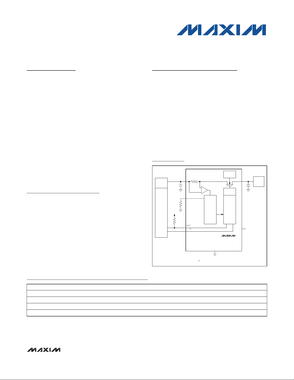
BIAS
VOLTAGE
POWER
SUPPLY
μP
10kΩ
V
PULLUP
OUTIN
1μF
CHARGE
PUMP
R
SETI
FLAG
ON(ON)*
CURRENT
REFERENCE
CONTROL
LOGIC
N.C.
MAX14523A
MAX14523AL
MAX14523B
MAX14523C
GND
LOAD
1μF
*ON FOR THE MAX14523AL ONLY.
Page 2
MAX14523A/MAX14523AL/MAX14523B/MAX14523C
250mA to 1.5A, Adjustable
Current-Limit Switches
2 _______________________________________________________________________________________
ABSOLUTE MAXIMUM RATINGS
ELECTRICAL CHARACTERISTICS
(VIN= +1.7V to +5.5V, R
SETI
= 94.2kΩ, CIN= C
OUT
= 1µF, and TA= TJ= -40°C to +125°C, unless otherwise noted. Typical values
are at V
IN
= +3.3V, TA= +25°C.) (Note 2)
Stresses beyond those listed under “Absolute Maximum Ratings” may cause permanent damage to the device. These are stress ratings only, and functional
operation of the device at these or any other conditions beyond those indicated in the operational sections of the specifications is not implied. Exposure to
absolute maximum rating conditions for extended periods may affect device reliability.
Note 1: Package thermal resistances were obtained using the method described in JEDEC specification JESD51-7, using a four-
layer board. For detailed information on package thermal considerations, refer to www.maxim-ic.com/thermal-turorial
.
(All voltages referenced to GND.)
IN, ON, ON, FLAG, OUT, and SETI to GND .............-0.3V to +6V
Current into Any Pin (Except IN, OUT)................................20mA
Out Short Circuit to GND...................................Internally Limited
Continuous Power Dissipation (T
A
= +70°C) for multilayer board:
8-Pin TDFN (derate 24.4mW/°C above +70°C) .........1952mW
Junction-to-Case Thermal Resistance (θ
JC
)
(Note 1) ...................................................................8.0°C/W
Junction-to-Ambient Thermal Resistance (θ
JA
)
(Note 1) .................................................................41.0°C/W
Operating Temperature Range .........................-40°C to +125°C
Junction Temperature......................................................+150°C
Storage Temperature Range .............................-65°C to +150°C
Lead Temperature (soldering, 10s) .................................+300°C
PARAMETER SYMBOL CONDITIONS MIN TYP MAX UNITS
SUPPLY OPERATION
Operating Voltage VIN 1.7 5.5 V
Quiescent Current IQ I
Latchoff Current I
Shutdown Forward Current I
Shutdown Re verse Current I
INTERNAL FET
Switch-On Resistance R
Forward-Current Limit I
(R
+2.48k) × I
SETI
Reverse Bloc king Current
Reverse Blocking Threshold V
FLAG Assertion Drop Voltage
Threshold
ON, ON INPUT
ON, ON Input Leakage I
ON, ON Input Logic-High Voltage V
ON, ON Input Logic-Low Voltage V
Product
LIM
LATCH
SHDN
RSHDN
ON
LIM
- VIN
OUT
V
FA
VON, VON = V
LEAK
IH
IL
= 0A, switch on, V
OUT
V
= 3.3V, I
IN
= 0A , after an overcurrent
OUT
fault (MAX14523B)
VON = 0V, VON = VIN, V
V
= 0V, VON = VIN, V
ON
5.5V (current into OUT)
VIN = 3.3V, I
R
= 91.78k, VIN - V
SETI
R
= 563.12k , VIN - V
SETI
I
= 250mA to 1500mA,
LIM
- V
V
IN
OUT
V
> VIN + 140mV, after reverse-current-
OUT
OUT
= 1V
lower than I
limit shutdown
V
- VIN = 300mV, OUT falling until
OUT
switch turns on
Increase (V
asserts, I
- V
IN
OUT
limiting, VIN = 3.3V
OUT
or V
IN
= 3.3V 170 300 μA
IN
10 20 μA
= 5.5V, V
IN
= 1.7V, V
IN
LIM
= 1V 1350 1500 1650
OUT
= 1V 225 250 275
OUT
= 0V 0.5 7 μA
OUT
=
OUT
0.01 0.6 μA
70 130 m
127.2 141.4 155.5 kV
2 μA
40 95 140 mV
) drop until FLAG
-1 +1 μA
GND
350 mV
1.6 V
0.4 V
mA
Page 3
MAX14523A/MAX14523AL/MAX14523B/MAX14523C
250mA to 1.5A, Adjustable
Current-Limit Switches
_______________________________________________________________________________________ 3
ELECTRICAL CHARACTERISTICS (continued)
(VIN= +1.7V to +5.5V, R
SETI
= 94.2kΩ, CIN= C
OUT
= 1µF, and TA= TJ= -40°C to +125°C, unless otherwise noted. Typical values
are at V
IN
= +3.3V, TA= +25°C.) (Note 2)
Note 2: All devices are 100% tested at 125°C. Electrical limits across the full temperature range are guaranteed by design and correlation.
Note 3: Blanking time and retry time are generated by the same oscillator. Therefore, the ratio of is a constant value of 32.
See Figures 2 and 3.
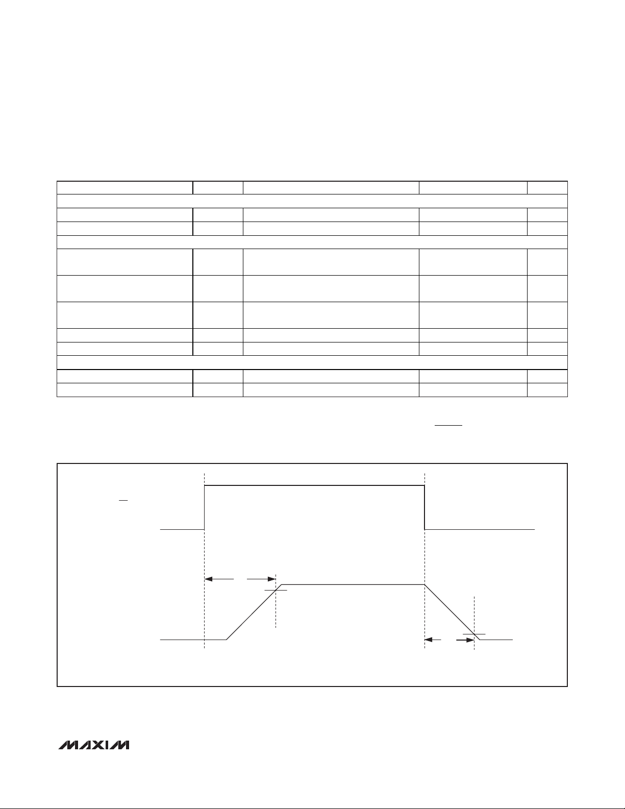
t
t
RETRY
BLANK
Figure 1. Timing Diagram for Measuring Turn-On Time (tSS) and Turn-Off Time (t
OFF
)
PARAMETER SYMBOL CONDITIONS MIN TYP MAX UNITS
FLAG OUTPUT
FLAG Output Logic-Low Voltage I
FLAG Output Lea kage Current VIN = V
DYNAMIC
Turn-On Time t
Turn-Off Time t
Current-Limit Reaction Time t
Blanking Time t
Retry Time t
THERMAL PROTECTION
Thermal Shutdown Low-to-high +170 °C
Thermal Shutdown Hysteresi s 15 °C
SS
OFF
LIM
BLANK
RETRY
= 1mA 0.4 V
SINK
= 5.5V, FLAG deas serted 1 μA
FLAG
Time from ENABLE signal to V
of V
= 3.3V, Figure 1
IN
Time from DISABLE signal to V
of V
= 3.3V, RL = 20, Figure 1
IN
V
= 3.3V, R
IN
output high and then short-circuit applied
= 91.78k to 563.12 k,
SETI
OUT
OUT
= 90%
= 10%
1 ms
250 μs
3 μs
(Note 3) 10 14.5 25 m s
MAX14523A/MAX14523AL (Note 3) 320 875 ms
ON(ON)*
t
SS
V
OUT
*( ) THE POLARITY OF THE SIGNAL IS REVERSED FOR THE MAX14523AL ONLY.
90% V
IN
10% V
t
OFF
IN
Page 4

MAX14523A/MAX14523AL/MAX14523B/MAX14523C
250mA to 1.5A, Adjustable
Current-Limit Switches
4 _______________________________________________________________________________________
Figure 2. Autoretry Fault Diagram
Figure 3. Latchoff Fault Diagram
OUT
CURRENT LIMIT
LOAD CURRENT
FLAG
t
BLANK
t
RETRY
t
BLANK
t
BLANK
t
RETRY
t
BLANK
t
BLANK
t
BLANK
THE DEVICE GOES TO
THERMAL-SHUTDOWN MODE
OUT
CURRENT LIMIT
LOAD CURRENT
THE DEVICE GOES TO
THERMAL-SHUTDOWN MODE
FLAG
Page 5

MAX14523A/MAX14523AL/MAX14523B/MAX14523C
250mA to 1.5A, Adjustable
Current-Limit Switches
_______________________________________________________________________________________ 5
Typical Operating Characteristics
(VIN= +3.3V, CIN= 1µF, C
OUT
= 1µF, R
SETI
= 94.2kΩ, TA= +25°C, unless otherwise noted.)
CURRENT LIMIT vs. SUPPLY VOLTAGE
1.60
1.55
1.50
CURRENT LIMIT (A)
1.45
1.40
1.70 5.50
SUPPLY VOLTAGE (V)
QUIESCENT SUPPLY CURRENT
vs. TEMPERATURE
300
250
VIN = +5V
200
150
QUIESCENT SUPPLY CURRENT (μA)
100
-40 125
VIN = +3.3V
TEMPERATURE (°C)
4.553.602.65
925926-7
NORMALIZED CURRENT LIMIT
1.10
MAX14523A toc01
1.05
1.00
0.95
NORMALIZED CURRENT LIMIT
0.90
-40 125
10
9
MAX14523A toc04
8
7
6
5
4
3
2
QUIESCENT SUPPLY CURRENT (μA)
1
0
-40 125
vs. TEMPERATURE
925926-7
TEMPERATURE (°C)
SHUTDOWN SUPPLY CURRENT
vs. TEMPERATURE
VON = 0V
VIN = +5V
VIN = +3.3V
925926-7
TEMPERATURE (°C)
MAX14523A toc02
MAX14523A toc05
QUIESCENT SUPPLY CURRENT
vs. SUPPLY VOLTAGE
300
250
200
150
QUIESCENT SUPPLY CURRENT (μA)
100
1.70 5.50
SUPPLY VOLTAGE (V)
4.553.602.65
SHUTDOWN FORWARD CURRENT
vs. TEMPERATURE
10
VON = 0V, V
9
8
7
6
5
4
3
2
SHUTDOWN FORWARD CURRENT (μA)
1
0
-40 125
= 0V
OUT
VIN = +5.5V
VIN = +1.7V
TEMPERATURE (°C)
MAX14523A toc03
MAX14523A toc06
925926-7
Page 6

MAX14523A/MAX14523AL/MAX14523B/MAX14523C
250mA to 1.5A, Adjustable
Current-Limit Switches
6 _______________________________________________________________________________________
Typical Operating Characteristics (continued)
(VIN= +3.3V, CIN= 1µF, C
OUT
= 1µF, R
SETI
= 94.2kΩ, TA= +25°C, unless otherwise noted.)
SHUTDOWN REVERSE CURRENT
vs. TEMPERATURE
10
VON = 0V, VIN = +1.7V, V
9
8
7
6
5
4
3
2
SHUTDOWN REVERSE CURRENT (μA)
1
0
-40 125
TEMPERATURE (°C)
OUT
= +5.5V
NORMALIZED ON-RESISTANCE
vs. SUPPLY TEMPERATURE
1.5
1.4
1.3
1.2
1.1
1.0
0.9
0.8
NORMALIZED ON-RESISTANCE
0.7
0.6
0.5
-40 125
TEMPERATURE (°C)
LATCHOFF CURRENT
vs. TEMPERATURE
30
MAX14523B
25
MAX14523A toc07
20
15
10
LATCHOFF CURRENT (μA)
5
0
925926-7
-40 125
VIN = +5.5V
VIN = +3.3V
925926-7
TEMPERATURE (°C)
1.20
1.15
MAX14523A toc08
1.10
1.05
1.00
0.95
0.90
NORMALIZED ON-RESISTANCE
0.85
0.80
SWITCH TURN-ON TIME
vs. SUPPLY TEMPERATURE
1.5
R
= 20Ω
LOAD
1.4
1.3
MAX14523A toc10
1.2
1.1
1.0
0.9
0.8
SWITCH TURN-ON TIME (ms)
0.7
0.6
0.5
925926-7
-40 125
VIN = +5.0V
VIN = +3.3V
925926-7
TEMPERATURE (°C)
1000
MAX14523A toc11
SWITCH TURN-OFF TIME (μs)
NORMALIZED ON-RESISTANCE
vs. SUPPLY VOLTAGE
1.70 5.50
VOLTAGE (V)
4.553.602.65
SWITCH TURN-OFF TIME
vs. SUPPLY TEMPERATURE
R
= 20Ω
LOAD
900
800
700
600
500
400
300
200
100
0
-40 125
VIN = +5.0V
VIN = +3.3V
925926-7
TEMPERATURE (°C)
MAX14523A toc09
MAX14523A toc12
Page 7

MAX14523A/MAX14523AL/MAX14523B/MAX14523C
250mA to 1.5A, Adjustable
Current-Limit Switches
_______________________________________________________________________________________ 7
Typical Operating Characteristics (continued)
(VIN= +3.3V, CIN= 1µF, C
OUT
= 1µF, R
SETI
= 94.2kΩ, TA= +25°C, unless otherwise noted.)
Pin Description
CURRENT LIMIT RESPONSE
SUDDEN SHORT
APPLIED AT OUTPUT
2μs/div
MAX14523A toc13
V
2V/div
I
OUT
10A/div
OUT
CURRENT LIMIT RESPONSE
R
= 16.5Ω TO SUDDEN SHORT
LOAD
APPLIED AT OUTPUT
20ms/div
MAX14523A toc14
V
OUT
2V/div
I
OUT
1A/div
FLAG RESPONSE (OVERLOAD CONDITION)
R
= 16.5Ω TO SUDDEN SHORT
LOAD
APPLIED AT OUTPUT
20ms/div
PIN
MAX14523A
MAX14523AL
MAX14523B
MAX14523C
1, 6 1, 6 N.C. No Connection. Not internall y connected. Connect N.C. to GND or leave unconnected.
2 2 FLAG
3 3 SETI
4 4 OUT Switch Output. Bypass OUT with a 1μF capacitor to GND.
5 5 IN
7 ON Active-Low, Switch-ON Input. Drive ON low to turn on the switch.
7 ON Active-High, Switch-ON Input. Drive ON high to turn on the switch.
8 8 GND Ground
— — EP
NAME FUNCTION
Open-Drain, Overload Indicator Output. FLAG goes low when the overload fault
duration exceeds the blan king time, reverse current is detected, thermal shutdown
mode is active, or SETI is connected to ground.
Overload-Current Limit Adjust. Connect a resistor from SETI to GND to program the
overcurrent limit. If SETI is connected to GND the switch turns off and FLAG is
asserted. If SETI is unconnected the current limit is at 0mA. Do not connect any
capacitance larger than 20pF to SETI.
Power Input. Bypass IN with a 1μF ceramic capacitor to GND. Use higher
capacitance if necessary to prevent large load transients from pulling down the
supply voltage.
Exposed Pad. Internally connected to GND. For enhanced thermal dissipation,
connect EP to a large copper ground plane. Do not use EP as the sole ground
connection.
MAX14523A toc15
V
FLAG
2V/div
I
OUT
1A/div
Page 8

MAX14523A/MAX14523AL/MAX14523B/MAX14523C
250mA to 1.5A, Adjustable
Current-Limit Switches
8 _______________________________________________________________________________________
Functional Diagram
Detailed Description
The MAX14523A/MAX14523AL/MAX14523B/MAX14523C
programmable current-limit switches operate from
+1.7V to +5.5V and provide internal current limiting
adjustable from 250mA to 1.5A. These devices feature
a fixed blanking time, and a FLAG output that notifies
the processor when a fault condition is present.
Programmable Current Limit/Threshold
A resistor from SETI to GND sets the current
limit/threshold for the switch (see the
Setting the
Current Limit/Threshold
section). If the output current is
limited at the current threshold value for a time equal to
or longer than t
BLANK
, the output flag asserts and the
MAX14523A/MAX14523AL enter the autoretry mode,
the MAX14523B latches off the switch, and the
MAX14523C enters the continuous current-limit mode.
Autoretry (MAX14523A/MAX14523AL)
When the forward current reaches the current threshold, the t
BLANK
timer begins counting (Figure 2). FLAG
asserts if the overcurrent condition is present for
t
BLANK
or longer. The timer resets if the overcurrent
condition disappears before the blanking time (t
BLANK
)
has elapsed. A retry time delay (t
RETRY
) starts immediately after the blanking time has elapsed. During that
time, the switch latches off. At the end of t
RETRY
, the
switch turns on again. If the fault still exists, the cycle
repeats. If the fault has been removed, the switch stays
on. During this cycle, FLAG stays low. In autoretry, if
the die temperature exceeds +170°C (typ) due to self
heating, the MAX14523A/MAX14523AL go into thermal
shutdown until the die temperature drops by approximately 15°C (see the
Thermal Shutdown
section.)
REVERSECURRENT
PROTECTION
IN
N.C.
MAX14523A
MAX14523AL
MAX14523B
MAX14523C
ON/(ON)*
*( ) FOR THE MAX14523AL ONLY
BUFFER
BANDGAP
REFERENCE
THERMAL
SHUTDOWN
CURRENT
LIMIT
GND
CONTROL
LOGIC
TIMING
CIRCUITRY
BUFFER
OUT
FLAG
SETI
Page 9

MAX14523A/MAX14523AL/MAX14523B/MAX14523C
250mA to 1.5A, Adjustable
Current-Limit Switches
_______________________________________________________________________________________ 9
The autoretry feature saves system power in case of an
overcurrent or short-circuit condition. During t
BLANK
time, when the switch is on, the supply current is held
at the current limit. During time t
RETRY
, when the switch
is off, the current through the switch is zero. Thus, the
average output current is much less than the programmed current limit. Calculate the average output
current using the following equation:
I
LOAD
= I
LIM
[(t
BLANK
)/(t
BLANK
+ t
RETRY
)]
With a typical t
BLANK
= 17.5ms and typical t
RETRY
=
560ms, the duty cycle is 3%, resulting in a 97% power
savings over the switch being on the entire time.
Latchoff (MAX14523B)
When the forward current reaches the current threshold, the t
BLANK
timer begins counting (Figure 3). FLAG
asserts if an overcurrent condition is present for greater
than t
BLANK
time. The timer resets if the overcurrent
condition disappears before t
BLANK
has elapsed.
The switch turns off if the overcurrent condition continues beyond the blanking time. Reset the switch by
either toggling the control logic (ON or ON) or cycling
the input voltage. If the die temperature exceeds
+170°C (typ) due to self heating, the MAX14523B goes
into thermal shutdown until the die temperature
drops by approximately 15°C (see the
Thermal
Shutdown
section).
Continuous Current Limit (MAX14523C)
When the forward current reaches the forward-current
threshold, the MAX14523C limits the output current to
the programmed current limit. FLAG asserts if the cur-
rent limit is present for t
BLANK
and deasserts when the
overload condition is removed. In this mode, if die temperature exceeds +170°C (typ) due to self heating, the
MAX14523C goes into thermal shutdown until the die
temperature drops by approximately 15°C (see the
Thermal Shutdown
section).
Switch-On/Off Control
The ON input for the MAX14523A/MAX14523B/
MAX14523C and ON input for the MAX14523AL control
the switch, see Table 1. Toggle ON for the MAX14523B
to reset the fault condition once the short-circuit current
is detected and the device shuts down.
Reverse-Current Protection
The MAX14523A/MAX14523AL/MAX14523B/MAX14523C
feature a reverse-current protection circuit that limits
the backflow current to 2µA when the reverse-current
protection circuitry has tripped. The switch turns off and
FLAG asserts without waiting for t
BLANK
to elapse. The
switch turns back on and FLAG deasserts when VINV
OUT
drops below the reverse-current threshold by
95mV (typ).
FLAG Indicator
FLAG is an open-drain fault indicator output and
requires an external pullup resistor to a DC supply.
FLAG goes low when any of the following conditions
occur:
• The blanking time has elapsed
• The reverse-current protection has tripped
• The die temperature exceeds +170°C
• SETI is connected to ground.
Thermal Shutdown
Thermal-shutdown circuitry protects the devices from
overheating. The switch turns off and FLAG goes low
immediately when the junction temperature exceeds
+170°C (typ). The switch turns on again after the
device temperature drops by approximately 15°C (typ).
Applications Information
Setting the Current Limit/Threshold
A resistor from SETI to ground programs the current
limit/threshold value for the MAX14523A/MAX14523AL/
MAX14523B/MAX14523C. Table 2 lists various current
limit/thresholds set by different resistor values at SETI.
Leaving SETI unconnected selects a 0 current
limit/threshold. Connecting SETI to ground asserts
FLAG.
Use the following formula to calculate the current limit:
Table 1. Switch Truth Table
MAX14523A
MAX14523B
MAX14523C
ON ON
0 1 Off
1 0 On
MAX14523AL
SWITCH STATUS
V
Rk
()
SETI
141400
()
ImA
()
LIM
k
.( )ΩΩ=−
248
Page 10

MAX14523A/MAX14523AL/MAX14523B/MAX14523C
250mA to 1.5A, Adjustable
Current-Limit Switches
Maxim cannot assume responsibility for use of any circuitry other than circuitry entirely embodied in a Maxim product. No circuit patent licenses are
implied. Maxim reserves the right to change the circuitry and specifications without notice at any time.
10
____________________Maxim Integrated Products, 120 San Gabriel Drive, Sunnyvale, CA 94086 408-737-7600
© 2009 Maxim Integrated Products Maxim is a registered trademark of Maxim Integrated Products, Inc.
Do not use an R
SETI
value smaller than 91.78kΩ.
Note: Connecting any capacitance larger than 20pF to
SETI can cause instability.
IN Bypass Capacitor
Connect a minimum of 1µF capacitor from IN to GND to
limit the input voltage drop during momentary output
short-circuit conditions. Larger capacitor values further
reduce the voltage undershoot at the input.
OUT Bypass Capacitor
For stable operation over the full temperature range
and over the full-programmable current-limit range, use
a 1µF ceramic capacitor from OUT to ground.
Excessive output capacitance can cause a false overcurrent condition due to decreased dv/dt across the
capacitor. Calculate the maximum capacitive load
(C
MAX
) value that can be connected to OUT using the
following formula:
For example, for V
IN
= 3.3V, t
BLANK
= 10ms, and I
LIM
=
300mA, C
MAX
equals 909µF.
Layout and Thermal Dissipation
To optimize the switch response time to output shortcircuit conditions, it is very important to keep all traces
as short as possible to reduce the effect of undesirable
parasitic inductance. Place input and output capacitors
as close as possible to the device (no more than 5mm).
IN and OUT must be connected with wide short traces
to the power bus. During normal operation, the power
dissipation is small and the package temperature
change is minimal. If the output is continuously shorted
to ground at the maximum supply voltage, the operation of the switches with the autoretry option does not
cause problems because the total power dissipated
during the short is scaled by the duty cycle:
Attention must be given to the MAX14523C continuous
current-limit version when the power dissipation during
a fault condition can cause the device to reach the thermal shutdown threshold.
Chip Information
PROCESS: BiCMOS
Table 2. Current Limit/Threshold vs.
Resistor Values
PACKAGE TYPE PACKAGE CODE DOCUMENT NO.
8 TDFN-EP T833+2
21-0137
Package Information
For the latest package outline information and land patterns, go to www.maxim-ic.com/packages.
Pin Configuration
R
(k) TYPICAL CURRENT LIMIT/THRESHOLD (mA)
SETI
91.78 1500
121 1145
221 632
301 466
422 333
563.12 250
(Open) 0
CµF
MAX
ImAt ms
() ()
LIM BLANK MIN
()
=
×
VV
IN
()
()
P
MAX
()
VI t
IN MAX OUT MA X BLA NK
=
××
() ()
tt
+
RETRY BLA
NNK
1
N.C.
2FLAG
3SETI
4OUT
+
MAX14523A
MAX14523AL
MAX14523B
MAX14523C
*EP
8 GND
7 ON(ON)**
6 N.C.
5IN
*CONNECT EXPOSED PAD TO GND.
**( ) FOR THE MAX14523AL ONLY.
TDFN
3mm x 3mm
 Loading...