

Page 1
General Description
The MAX1449 +3.3V, 10-bit analog-to-digital converter
(ADC) features a fully differential input, a pipelined 10stage ADC architecture with wideband track-and-hold
(T/H), and digital error correction incorporating a fully
differential signal path. The ADC is optimized for lowpower, high-dynamic performance in imaging and digital communications applications. The converter
operates from a single +2.7V to +3.6V supply, consuming only 186mW while delivering a 58.5dB (typ) signalto-noise ratio (SNR) at a 20MHz input frequency. The
fully differential input stage has a -3dB 400MHz bandwidth and may be operated with single-ended inputs. In
addition to low operating power, the MAX1449 features
a 5µA power-down mode for idle periods.
An internal +2.048V precision bandgap reference is
used to set the ADC’s full-scale range. A flexible reference structure allow’s the user to supply a buffered,
direct, or externally derived reference for applications
requiring increased accuracy or a different input voltage range.
Lower speed, pin-compatible versions of the MAX1449
are also available. Refer to the MAX1444 data sheet for
a 40Msps version, the MAX1446 data sheet for a
60Msps version, and the MAX1448 data sheet for 80Msps.
The MAX1449 has parallel, offset binary, CMOS-compatible, three-state outputs that can be operated from
+1.7V to +3.6V to allow flexible interfacing. The device
is available in a 5mm x 5mm 32-pin TQFP package and
is specified over the extended industrial (-40°C to
+85°C) temperature range.
________________________Applications
Ultrasound Imaging
CCD Imaging
Baseband and IF Digitization
Digital Set-Top Boxes
Video Digitizing Applications
Features
♦ Single +3.3V Operation
♦ Excellent Dynamic Performance
58.5dB SNR at f
IN
= 20MHz
72dBc SFDR at f
IN
= 20MHz
♦ Low Power
62mA (Normal Operation)
5µA (Shutdown Mode)
♦ Fully Differential Analog Input
♦ Wide 2Vp-p Differential Input Voltage Range
♦ 400MHz -3dB Input Bandwidth
♦ On-Chip +2.048V Precision Bandgap Reference
♦ CMOS-Compatible Three-State Outputs
♦ 32-Pin TQFP Package
♦ Evaluation Kit Available
MAX1449
10-Bit, 105Msps, Single +3.3V, Low-Power
ADC with Internal Reference
________________________________________________________________ Maxim Integrated Products 1
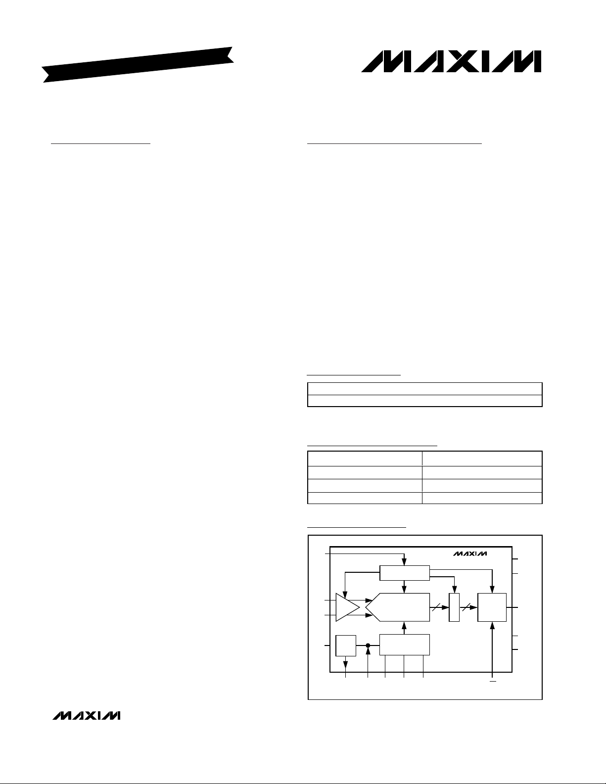
Functional Diagram
19-4802; Rev 0; 10/00
EVALUATION KIT AVAILABLE
Ordering Information
Pin Configuration appears at end of data sheet.
Pin-Compatible, Lower Speed
Selection Table
For price, delivery, and to place orders, please contact Maxim Distribution at 1-888-629-4642,
or visit Maxim’s website at www.maxim-ic.com.
PART TEMP. RANGE PIN-PACKAGE
MAX1449EHJ -40°C to +85°C 32 TQFP
PART NUMBER SAMPLING SPEED
MAX1444 40Msps
MAX1446 60Msps
MAX1448 80Msps
CLK
IN+
T/H
IN-
PD
REF
REFINREFOUT REFP COM REFN OE
MAX1449
CONTROL
10
D
OUTPUT
PIPELINE ADC
REF SYSTEM +
BIAS
E
DRIVERS
C
V
DD
GND
D9–D0
OV
DD
OGND
Page 2
MAX1449
10-Bit, 105Msps, Single +3.3V, Low-Power
ADC with Internal Reference
2 _______________________________________________________________________________________
ABSOLUTE MAXIMUM RATINGS
ELECTRICAL CHARACTERISTICS
(VDD= +3.3V, OVDD= +2.0V; 0.1µF and 1.0µF capacitors from REFP, REFN, and COM to GND; V
REFIN
= +2.048V, REFOUT
connected to REFIN through a 10kΩ resistor, V
IN
= 2Vp-p (differential with respect to COM), CL ≈ 10pF at digital outputs, f
CLK
=
105MHz, T
A
= T
MIN
to T
MAX
, unless otherwise noted. Typical values are at T
A
=
+25°C.)
Stresses beyond those listed under “Absolute Maximum Ratings” may cause permanent damage to the device. These are stress ratings only, and functional
operation of the device at these or any other conditions beyond those indicated in the operational sections of the specifications is not implied. Exposure to
absolute maximum rating conditions for extended periods may affect device reliability.
VDD, OVDDto GND ...............................................-0.3V to +3.6V
OGND to GND.......................................................-0.3V to +0.3V
IN+, IN- to GND........................................................-0.3V to V
DD
REFIN, REFOUT, REFP,
REFN, and COM to GND..........................-0.3V to (V
DD
+ 0.3V)
OE, PD, CLK to GND..................................-0.3V to (V
DD
+ 0.3V)
D9–D0 to GND.........................................-0.3V to (OV
DD
+ 0.3V)
Continuous Power Dissipation (T
A
= +70°C)
32-Pin TQFP (derate 11.1mW/°C above +70°C)...........889mW
Operating Temperature Range ...........................-40°C to +85°C
Junction Temperature......................................................+150°C
Storage Temperature Range ............................-60°C to +150°C
Lead Temperature (soldering, 10s) .................................+300°C
DC ACCURACY
Resolution 10 Bits
Integral Nonlinearity INL fIN = 7.5MHz ±0.75 ±2.4 LSB
Differential Nonlinearity DNL fIN = 7.5MHz, no missing codes guaranteed ±0.5 ±1.0 LSB
Offset Error < ±1 ±1.7 % FS
Gain Error 0 ±2% FS
ANALOG INPUT
Input Differential Range V
Common-Mode
Voltage Range
Input Resistance R
Input Capacitance C
CONVERSION RATE
Maximum Clock Frequency f
Data Latency 5.5 Cycles
DYNAMIC CHARACTERISTICS (f
Signal-To-Noise Ratio
(Note 1)
Signal-To-Noise And Distortion
(Up to 5
Spurious-Free Dynamic
Range (Note 1)
PARAMETER SYMBOL CONDITIONS MIN TYP MAX UNITS
th
Harmonic) (Note 1)
DIFF
V
COM
IN
IN
CLK
= 105.26MHz, 4096-point FFT)
CLK
SNR
SINAD
SFDR
Differential or single-ended inputs ±1.0 V
Switched capacitor load 20 kΩ
f
= 7.5MHz 56.3 58.5
IN
fIN = 20MHz 55.8 58.5 dB
f
= 50MHz 58
IN
fIN = 7.5MHz 55.3 58.2
fIN = 20MHz 55.1 58.1 dB
f
= 50MHz 57.6
IN
fIN = 7.5MHz 61 72
fIN = 20MHz, TA = +25°C 63 72 dBc
f
= 50MHz 70
IN
105 MHz
VDD/2
± 0.5
5pF
V
Page 3
MAX1449
10-Bit, 105Msps, Single +3.3V, Low-Power
ADC with Internal Reference
_______________________________________________________________________________________ 3
ELECTRICAL CHARACTERISTICS (continued)
(VDD= +3.3V, OVDD= +2.0V; 0.1µF and 1.0µF capacitors from REFP, REFN, and COM to GND; V
REFIN
= +2.048V, REFOUT
connected to REFIN through a 10kΩ resistor, V
IN
= 2Vp-p (differential with respect to COM), CL≈ 10pF at digital outputs, f
CLK
=
105MHz, T
A
= T
MIN
to T
MAX
, unless otherwise noted. Typical values are at T
A
=
+25°C.)
Third-Harmonic Distortion
(Note 1)
Intermodulation Distortion (First 5
Odd-Order IMDs) (Note 2)
Third-Order Intermodulation
Distortion (Note 2)
PARAMETER SYMBOL CONDITIONS MIN TYP MAX UNITS
HD3
IMD
IM3
Total Harmonic Distortion
(First 5 Harmonics)
THD
(Note 1)
fIN = 7.5MHz -72
fIN = 20MHz -72
f
= 50MHz -70
IN
f
= 38MHz at -6.5dB FS
1
= 42MHz at -6.5dB FS
f
2
f
= 38MHz at -6.5dB FS
1
f
= 42MHz at -6.5dB FS
2
fIN = 7.5MHz, TA = +25°C -70 -61.5
fIN = 20MHz, TA = +25°C -70 -61.5 dBc
= 50MHz -70
f
IN
Small-Signal Bandwidth Input at -20dB FS, differential inputs 500 MHz
Full-Power Bandwidth FPBW Input at -0.5dB FS, differential inputs 400 MHz
Aperture Delay t
Aperture Jitter t
AD
AJ
Overdrive Recovery Time For 1.5 x full-scale input 2 ns
Differential Gain ±1%
Differential Phase ±0.25 degree
Output Noise IN+ = IN- = COM 0.2 LS B
INTERNAL REFERENCE
Reference Output Voltage REFOUT
Reference Temperature
Coefficient
TC
REF
Load Regulation 1.25 mV/mA
EXTERNAL REFERENCE
Positive Reference REFP V
Negative Reference REFN V
Differential Reference Voltage ∆V
REFIN Resistance R
REF
REFIN
= +2.048V 2.162 V
REFIN
= +2.048V 1.138 V
REFIN
V
-V
, V
REFP
REFN
= +2.048V 0.98 1.024 1.07 V
REFIN
DIGITAL INPUTS (CLK, PD, OE)
0.8 x
V
DD
0.8 x
V
DD
Input High Threshold V
CLK
IH
PD, OE
CLK
Input Low Threshold V
IL
PD, OE
dBc
-76 dBc
-76 dBc
1ns
2ps
2.048
±1%
RMS
RM S
V
60 ppm/°C
>50 MΩ
V
0.2 x
V
DD
0.2 x
V
DD
V
Page 4
Note 1: SNR, SINAD, THD, SFDR and HD3 are based on an analog input voltage of -0.5dB FS referenced to a +1.024V full-scale
input voltage range.
Note 2: Intermodulation distortion is the total power of the intermodulation products relative to the individual carrier. This number is
6dB better if referenced to the two-tone envelope.
Note 3: Digital outputs settle to V
IH,VIL
.
Note 4: With REFIN driven externally, REFP, COM, and REFN are left floating while powered down.
MAX1449
10-Bit, 105Msps, Single +3.3V, Low-Power
ADC with Internal Reference
4 _______________________________________________________________________________________
ELECTRICAL CHARACTERISTICS (continued)
(VDD= +3.3V, OVDD= +2.0V; 0.1µF and 1.0µF capacitors from REFP, REFN, and COM to GND; V
REFIN
= +2.048V, REFOUT
connected to REFIN through a 10kΩ resistor, V
IN
= 2Vp-p (differential with respect to COM), CL≈ 10pF at digital outputs,
f
CLK
= 105MHz, TA= T
MIN
to T
MAX
, unless otherwise noted. Typical values are at T
A
=
+25°C.)
PARAMETER SYMBOL CONDITIONS MIN TYP MAX UNITS
Input Hysteresis V
Input Leakage
Input Capacitance C
HYST
I
I
IH
IL
IN
VIH = VDD = OV
DD
VIL = 0 ±5
DIGITAL OUTPUTS (D9–D0)
Output Voltage Low V
Output Voltage High V
Three-State Leakage Current I
Three-State Output Capacitance C
LEAK
OUT
OL
OH
I
= 200µA 0.2 V
SINK
I
OE = OV
OE = OV
SOURCE
= 200µA
DD
DD
POWER REQUIREMENTS
Analog Supply Voltage V
Output Supply Voltage OV
Analog Supply Current I
DD
DD
VDD
Operating, fIN = 20MHz at -0.5dB FS 58 74 mA
Shutdown, clock idle, PD = OE = OV
DD
Operating, CL = 15pF , fIN = 20MHz at
Output Supply Current I
OVDD
Power Supply Rejection PSRR
-0.5dB FS
Shutdown, clock idle, PD = OE = OV
DD
Offset ±0.1 mV/V
Gain ±0.1 %/V
TIMING CHARACTERISTICS
CLK Rise-to-Output Data Valid t
OE Fall-to-Output Enable t
OE Rise-to-Output Disable t
ENABLE
DISABLE
CLK Pulse Width High t
CLK Pulse Width Low t
Wake-Up Time t
DO
CH
WAKE
Figure 6 (Note 3) 5 8 ns
Figure 5 10 ns
Figure 5 15 ns
Figure 6, clock period 9.52ns
Figure 6, clock period 9.52ns
CL
(Note 4) 1.5 µs
OV
DD
- 0.2
2.7 3.3 3.6 V
1.7 3.3 3.6 V
0.1 V
±5 µA
5pF
V
±10 µA
5pF
415µA
10 mA
110µA
4.76
±0.47
4.76
±0.47
ns
ns
Page 5
MAX1449
10-Bit, 105Msps, Single +3.3V, Low-Power
ADC with Internal Reference
_______________________________________________________________________________________ 5
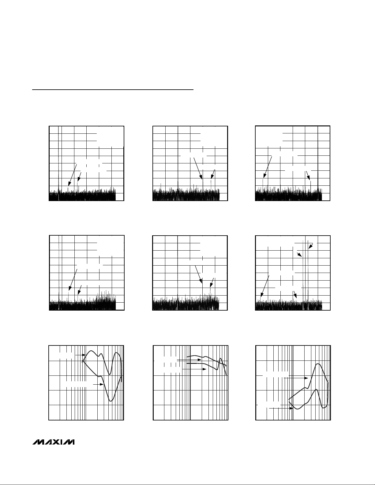
Typical Operating Characteristics
(VDD= +3.3V, OVDD= +2.0V, internal reference, differential input at -0.5dB FS, f
CLK
= 106.2345MHz, CL≈ 10pF, TA= +25°C,
unless otherwise noted.)
FFT PLOT (fIN = 7.5MHz,
8192-POINT FFT, DIFFERENTIAL INPUT)
0
-10
-20
-30
-40
-50
-60
AMPLITUDE (dB)
-70
-80
-90
-100
02010 30 40 50 60
2ND HARMONIC
3RD HARMONIC
ANALOG INPUT FREQUENCY (MHz)
FFT PLOT (fIN = 7.5MHz,
8192-POINT FFT, SINGLE-ENDED INPUT)
0
-10
-20
-30
-40
-50
-60
AMPLITUDE (dB)
-70
-80
-90
-100
02010 30 40 50 60
2ND HARMONIC
3RD HARMONIC
ANALOG INPUT FREQUENCY (MHz)
SNR = 58.6dB
SINAD = 58.4dB
THD = -72.7dBc
SFDR = 73.6dBc
SNR = 57.7dB
SINAD = 57.5dB
THD = -71.8dBc
SFDR = 74.4dBc
MAX1449 toc01
MAX1449 toc04
-10
-20
-30
-40
-50
-60
AMPLITUDE (dB)
-70
-80
-90
-100
-10
-20
-30
-40
-50
-60
AMPLITUDE (dB)
-70
-80
-90
-100
FFT PLOT (fIN = 19.99MHz,
8192-POINT FFT, DIFFERENTIAL INPUT)
0
2ND HARMONIC
02010 30 40 50 60
ANALOG INPUT FREQUENCY (MHz)
SNR = 58.5dB
SINAD = 58.4dB
THD = -73.7dBc
SFDR = 75.9dBc
3RD HARMONIC
FFT PLOT (fIN = 19.99MHz,
8192-POINT FFT, SINGLE-ENDED INPUT)
0
2ND HARMONIC
02010 30 40 50 60
ANALOG INPUT FREQUENCY (MHz)
SNR = 57.7dB
SINAD = 57.2dB
THD = -67dBc
SFDR = 67.7dBc
3RD HARMONIC
UNDERSAMPLING FFT PLOT (fIN = 50.12MHz,
8192-POINT FFT, DIFFERENTIAL INPUT)
0
SNR = 57.9dB
-10
SINAD = 56.7dB
MAX1449 toc02
THD = -71.3dBc
-20
SFDR = 71.1dBc
-30
-40
-50
-60
AMPLITUDE (dB)
-70
-80
-90
-100
2ND HARMONIC
3RD HARMONIC
02010 30 40 50 60
ANALOG INPUT FREQUENCY (MHz)
TWO-TONE INTERMODULATION
(8192-POINT IMD, DIFFERENTIAL INPUT)
0
f1 = 38MHz AT -6.5dB FS
-10
= 42MHz AT -6.5dB FS
f
MAX1449 toc05
2
-20
-30
-40
-50
-60
AMPLITUDE (dB)
-70
-80
-90
-100
2ND ORDER IMD
02010 30 40 50 60
ANALOG INPUT FREQUENCY (MHz)
f
3RD ORDER IMD
MAX1449 toc03
f
2
1
MAX1449 toc06
SPURIOUS-FREE DYNAMIC RANGE
vs. ANALOG INPUT FREQUENCY
80
DIFFERENTIAL
74
68
SFDR (dBc)
62
56
50
SINGLE-ENDED
110100
ANALOG INPUT FREQUENCY (MHz)
MAX1449 toc07
SIGNAL-TO-NOISE RATIO
vs. ANALOG INPUT FREQUENCY
60
DIFFERENTIAL
58
SINGLE-ENDED
56
SNR (dB)
54
52
50
110100
ANALOG INPUT FREQUENCY (MHz)
MAX1449 toc08
TOTAL HARMONIC DISTORTION
vs. ANALOG INPUT FREQUENCY
-50
-56
-62
THD (dBc)
-68
-74
-80
SINGLE-ENDED
DIFFERENTIAL
1 10 100
ANALOG INPUT FREQUENCY (MHz)
MAX1449 toc09
Page 6
MAX1449
10-Bit, 105Msps, Single +3.3V, Low-Power
ADC with Internal Reference
6 _______________________________________________________________________________________
Typical Operating Characteristics (continued)
(VDD= +3.3V, OVDD= +2.0V, internal reference, differential input at -0.5dB FS, f
CLK
= 106.2345MHz, CL≈ 10pF, TA= +25°C,
unless otherwise noted.)
SIGNAL-T0-NOISE PLUS DISTORTION
vs. ANALOG INPUT FREQUENCY
60
DIFFERENTIAL
58
56
SINAD (dB)
54
52
50
SINGLE-ENDED
1 10 100
ANALOG INPUT FREQUENCY (MHz)
MAX1449 toc10
FULL-POWER INPUT BANDWIDTH vs.
ANALOG INPUT FREQUENCY, SINGLE-ENDED
6
4
2
0
-2
AMPLITUDE (dB)
-4
-6
-8
1 100010010
ANALOG INPUT FREQUENCY (MHz)
SMALL-SIGNAL INPUT BANDWIDTH vs.
ANALOG INPUT FREQUENCY, SINGLE-ENDED
6
VIN = 100mVp-p
4
MAX1449 toc11
2
0
-2
AMPLITUDE (dB)
-4
-6
-8
1 100010010
ANALOG INPUT FREQUENCY (MHz)
MAX1449 toc12
SPURIOUS-FREE DYNAMIC RANGE
vs. INPUT POWER (f
80
75
70
65
SFDR (dBc)
60
55
50
-12 -6-9 -3 0
INPUT POWER (dB FS)
= 19MHz)
IN
SIGNAL-TO-NOISE + DISTORTION vs.
= 19MHz)
IN
65
60
55
SINAD (dB)
50
INPUT POWER (f
MAX1449 toc13
MAX1449 toc16
SIGNAL-TO-NOISE RATIO vs.
INPUT POWER (f
65
60
55
SNR (dB)
50
45
40
-12 -6-9 -3 0
INPUT POWER (dB FS)
= 19MHz)
IN
SPURIOUS-FREE DYNAMIC RANGE
vs. TEMPERATURE
84
fIN = 26.1696MHz
80
76
SFDR (dBc)
72
MAX1449 toc14
MAX1449 toc17
TOTAL HARMONIC DISTORTION
vs. INPUT POWER (f
-50
-55
-60
-65
THD (dBc)
-70
-75
-80
-12 -6-9 -3 0
INPUT POWER (dB FS)
= 19MHz)
IN
SIGNAL-TO-NOISE vs. TEMPERATURE
70
fIN = 26.1696MHz
66
62
SNR (dB)
58
MAX1449 toc15
MAX1449 toc18
45
40
-12 -6-9 -3 0
INPUT POWER (dB FS)
68
64
-40 10-15 35 60 85
TEMPERATURE (°C)
54
50
-40 10-15 35 60 85
TEMPERATURE (°C)
Page 7
MAX1449
10-Bit, 105Msps, Single +3.3V, Low-Power
ADC with Internal Reference
_______________________________________________________________________________________ 7
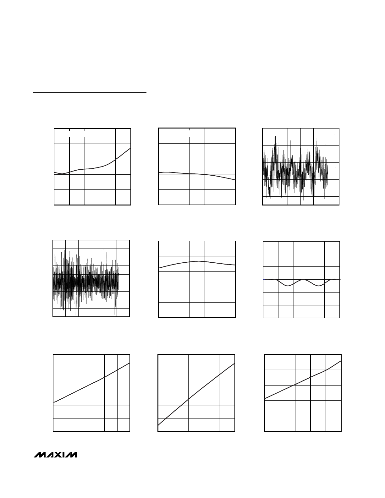
Typical Operating Characteristics (continued)
(VDD= +3.3V, OVDD= +2.0V, internal reference, differential input at -0.5dB FS, f
CLK
= 106.2345MHz, CL≈ 10pF, TA= +25°C,
unless otherwise noted.)
TOTAL HARMONIC DISTORTION
vs. TEMPERATURE
-60
fIN = 26.1696MHz
-64
-68
THD (dBc)
-72
-76
-80
-40 10-15 35 60 85
TEMPERATURE (°C)
DIFFERENTIAL NONLINEARITY vs.
DIGITAL OUTPUT CODE
0.5
0.4
0.3
0.2
0.1
0
DNL (LSB)
-0.1
-0.2
-0.3
-0.4
0400200 600 800 1000 1200
DIGITAL OUTPUT CODE
MAX1449 toc19
SINAD (dB)
MAX1449 toc22
GAIN ERROR (LSB)
SIGNAL-TO-NOISE + DISTORTION
vs. TEMPERATURE
70
fIN = 26.1696MHz
66
62
58
54
50
-40 10-15 35 60 85
TEMPERATURE (°C)
GAIN ERROR vs. TEMPERATURE,
EXTERNAL REFERENCE, V
0.10
0.08
0.06
0.04
0.02
0
-40 10-15 35 60 85
TEMPERATURE (°C)
REFIN
INTEGRAL NONLINEARITY vs.
DIGITAL OUTPUT CODE (BEST STRAIGHT LINE)
0.5
0.4
MAX1449 toc20
0.3
0.2
0.1
INL (LSB)
0
-0.1
-0.2
-0.3
-0.4
0 400200 600 800 1000 1200
DIGITAL OUTPUT CODE
OFFSET ERROR vs. TEMPERATURE,
= +2.048V
MAX1449 toc23
EXTERNAL REFERENCE, V
4
3
2
1
0
OFFSET ERROR (LSB)
-1
-2
-40 10-15 35 60 85
TEMPERATURE (°C)
REFIN
MAX1449 toc21
= +2.048V
MAX1449 toc24
ANALOG SUPPLY CURRENT
vs. ANALOG SUPPLY VOLTAGE
63
61
59
(mA)
57
VDD
I
55
53
51
2.70 3.00 3.152.85 3.30 3.45 3.60
VDD (V)
MAX1449 toc25
ANALOG SUPPLY CURRENT
vs. TEMPERATURE
70
65
60
(mA)
55
VDD
I
50
45
40
-40 10-15 356085
TEMPERATURE (°C)
MAX1449 toc26
DIGITAL SUPPLY CURRENT
vs. TEMPERATURE
15
12
9
(mA)
OVDD
I
6
3
0
-40 10-15 35 60 85
TEMPERATURE (°C)
MAX1449 toc27
Page 8

MAX1449
10-Bit, 105Msps, Single +3.3V, Low-Power
ADC with Internal Reference
8 _______________________________________________________________________________________
Typical Operating Characteristics (continued)
(VDD= +3.3V, OVDD= +2.0V, internal reference, differential input at -0.5dB FS, f
CLK
= 106.2345MHz, CL≈ 10pF, TA= +25°C,
unless otherwise noted.)
12
DIGITAL SUPPLY CURRENT
vs. TEMPERATURE
ANALOG POWER-DOWN CURRENT
vs. ANALOG SUPPLY VOLTAGE
3.00
DIGITAL POWER-DOWN CURRENT
vs. DIGITAL SUPPLY VOLTAGE
12
10
(mA)
8
OVDD
I
6
4
-40 10-15 35 60 85
TEMPERATURE (°C)
MAX1449 toc28
2.80
2.60
(µA)
VDD
I
2.40
2.20
2.00
2.70 3.002.85 3.15 3.30 3.45 3.60
SFDR, SNR, THD, SINAD
vs. CLOCK FREQUENCY
80
fIN = 50.123MHz
75
70
65
60
SFDR, SNR, THD, SINAD (dB)
55
50
100 108104 112 116 120
SFDR
THD
SNR
SINAD
CLOCK FREQUENCY (MHz)
INTERNAL REFERENCE VOLTAGE
vs. TEMPERATURE
2.10
2.08
2.06
(V)
REF
V
2.04
2.02
2.00
-40 10-15 35 60 85
TEMPERATURE (°C)
VDD (V)
MAX1449 toc31
MAX1449 toc33
MAX1449 toc29
9
(µA)
6
OVDD
I
3
0
2.0 2.62.3 3.0 3.3 3.6
INTERNAL REFERENCE VOLTAGE
vs. ANALOG SUPPLY VOLTAGE
2.100
2.075
(V)
2.050
REF
V
2.025
2.000
2.70 3.152.85 3.00 3.30 3.45 3.60
VDD (V)
OUTPUT NOISE HISTOGRAM (DC INPUT)
70,000
60,000
50,000
40,000
COUNTS
30,000
20,000
10,000
0
0
N-2 NN-1 N+1 N+2
64676
607
DIGITAL OUTPUT CODE
MAX1449 toc30
OV
(V)
DD
MAX1449 toc32
MAX1449 toc34
252
0
Page 9

MAX1449
10-Bit, 105Msps, Single +3.3V, Low-Power
ADC with Internal Reference
_______________________________________________________________________________________ 9
Pin Description
PIN NAME FUNCTION
1 REFN
2 COM Common-Mode Voltage Output. Bypass to GND with a > 0.1µF capacitor.
3, 9, 10 V
4, 5, 8, 11,
14, 30
6 IN+ Positive Analog Input. For single-ended operation connect signal source to IN+.
7 IN- Negative Analog Input. For single-ended operation connect IN- to COM.
12 CLK Conversion Clock Input
13 PD
15 OE
16–20 D9–D5 Three-State Digital Outputs D9–D5. D9 is the MSB.
21 OV
22 T.P. Test Point. Do not connect.
23 OGND Output Driver Ground
DD
GND Analog Ground
DD
Lower Reference. Conversion range is ±(V
Bypass to GND with a > 0.1µF capacitor.
Analog Supply Voltage. Bypass to GND with a capacitor combination of 2.2µF in parallel with 0.1µF.
Power Down Input.
High: Power-down mode
Low: Normal operation
Output Enable Input.
High: Digital outputs disabled
Low: Digital outputs enabled
Output Driver Supply Voltage. Bypass to GND with a capacitor combination of 2.2µF in parallel with
0.1µF.
REFP
- V
REFN
).
24–28 D4–D0 Three-State Digital Outputs D4–D0. D0 is the LSB.
29 REFOUT
31 REFIN Reference Input. V
32 REFP Upper Reference. Conversion range is ±(V
Internal Reference Voltage Output. May be connected to REFIN through a resistor or a resistordivider.
REFIN
= 2 ✕ (V
REFP
- V
). Bypass to GND with a > 0.1µF capacitor.
REFN
- V
REFP
). Bypass to GND with a > 0.1µF capacitor.
REFN
Page 10

MAX1449
10-Bit, 105Msps, Single +3.3V, Low-Power
ADC with Internal Reference
10 ______________________________________________________________________________________
Detailed Description
The MAX1449 uses a 10-stage, fully differential,
pipelined architecture (Figure 1), that allows for highspeed conversion while minimizing power consumption. Each sample moves through a pipeline stage
every half-clock cycle. Counting the delay through the
output latch, the clock-cycle latency is 5.5.
A 1.5-bit (2-comparator) flash ADC converts the held
input voltage into a digital code. The following digitalto-analog converter (DAC) converts the digitized result
back into an analog voltage, which is then subtracted
from the original held input signal. The resulting error
signal is then multiplied by two, and the product is
passed along to the next pipeline stage where the
process is repeated until the signal has been
processed by all 10 stages. Each stage provides a 1bit resolution. Digital error-correction compensates for
ADC comparator offsets in each pipeline stage and
ensures no missing codes.
Input Track-and-Hold (T/H) Circuit
Figure 2 displays a simplified functional diagram of the
input track-and-hold (T/H) circuit in both track and hold
mode. In track mode, switches S1, S2a, S2b, S4a, S4b,
S5a and S5b are closed. The fully differential circuit
samples the input signal onto the two capacitors C2a
and C2b through switches S4a and S4b. Switches S2a
and S2b set the common mode for the amplifier input,
and open simultaneously with S1, sampling the input
waveform. Switches S4a and S4b are then opened
before switches S3a and S3b connect capacitors C1a
and C1b to the output of the amplifier and switch S4c is
closed. The resulting differential voltage is held on
capacitors C2a and C2b. The amplifier is used to
charge capacitors C1a and C1b to the same values
originally held on C2a and C2b. This value is then presented to the first stage quantizer and isolates the
pipeline from the fast-changing input. The wide input
bandwidth T/H amplifier allows the MAX1449 to track
and sample/hold analog inputs of high frequencies
beyond Nyquist. The analog inputs IN+ and IN- can be
driven either differentially or single-ended. It is recommended to match the impedance of IN+ and IN- and
set the common-mode voltage to mid-supply (V
DD
/2)
for optimum performance.
Analog Input and Reference Configuration
The full-scale range of the MAX1449 is determined by the
internally generated voltage difference between REFP
(VDD/2 + V
REFIN
/4) and REFN (VDD/2 - V
REFIN
/4). The
ADC’s full-scale range is user-adjustable through the
REFIN pin, which provides a high input impedance for
this purpose. REFOUT, REFP, COM (VDD/2), and REFN
are internally buffered low-impedance outputs.
Figure 1. Pipelined Architecture—Stage Blocks
Figure 2. Internal T/H Circuit
MDAC
V
IN
FLASH
ADC
T/H
1.5 BITS
Σ
DAC
V
OUT
x2
IN+
IN-
S4a
S4b
S4c
C2a
C2b
INTERNAL
BIAS
S2a
S1
C1a
C1b
COM
S5a
S3a
OUT
OUT
V
IN
STAGE 1 STAGE 2
DIGITAL CORRECTION LOGIC
10
V
= INPUT VOLTAGE BETWEEN
IN
IN+ AND IN- (DIFFERENTIAL OR SINGLE-ENDED)
D9–D0
STAGE 10
TRACK TRACK
HOLD HOLD
INTERNAL
BIAS
CLK
INTERNAL
NON-OVERLAPPING
CLOCK SIGNALS
S3b
S5bS2b
COM
Page 11

MAX1449
10-Bit, 105Msps, Single +3.3V, Low-Power
ADC with Internal Reference
______________________________________________________________________________________ 11
The MAX1449 provides three modes of reference operation:
• Internal reference mode
• Buffered external reference mode
• Unbuffered external reference mode
In internal reference mode, the internal reference output REFOUT can be tied to the REFIN pin through a
resistor (e.g., 10kΩ) or resistor-divider, if an application
requires a reduced full-scale range. For stability purposes it is recommended to bypass REFIN with a
>10nF capacitor to GND.
In buffered external reference mode, the reference voltage levels can be adjusted externally by applying a
stable and accurate voltage at REFIN. In this mode,
REFOUT may be left open or connected to REFIN
through a >10kΩ resistor.
In unbuffered external reference mode, REFIN is connected to GND thereby deactivating the on-chip buffers
of REFP, COM, and REFN. With their buffers shut down,
these pins become high impedance and can be driven
by external reference sources.
Clock Input (CLK)
The MAX1449’s CLK input accepts CMOS-compatible
clock signals. Since the inter-stage conversion of the
device depends on the repeatability of the rising and
falling edges of the external clock, use a clock with low
jitter and fast rise and fall times (<2ns). In particular,
sampling occurs on the falling edge of the clock signal,
mandating this edge to provide lowest possible jitter.
Any significant aperture jitter would limit the SNR performance of the ADC as follows:
SNR = 20 × log (0.5 × π × f
IN
× tAJ)
where fINrepresents the analog input frequency and
tAJis the time of the aperture jitter.
Clock jitter is especially critical for undersampling
applications. The clock input should always be consid-
ered as an analog input and routed away from any analog input or other digital signal lines.
The MAX1449 clock input operates with a voltage
threshold set to VDD/2. Clock inputs with a duty cycle
other than 50% must meet the specifications for high
and low periods as stated in the Electrical
Characteristics. (See Figures 3 (3a, 3b) and 4 (4a, 4b)
for the relationship between spurious-free dynamic
range (SFDR), signal-to-noise ratio (SNR), total harmonic distortion (THD), or signal-to-noise plus distortion
(SINAD) versus duty cycle.)
Output Enable (
OOEE
), Power Down (PD),
and Output Data (D0–D9)
All data outputs, D0 (LSB) through D9 (MSB), are
TTL/CMOS logic-compatible. There is a 5.5 clock-cycle
latency between any particular sample and its valid
output data. The output coding is straight offset binary
(Table 1). With OE and PD high, the digital outputs
enter a high-impedance state. If OE is held low with PD
high, the outputs are latched at the last value prior to
the power down.
The capacitive load on the digital outputs D0 through D9
should be kept as low as possible (<15pF), to avoid
large digital currents that could feed back into the analog portion of the MAX1449, thereby degrading its
dynamic performance. The use of buffers on the digital
outputs of the ADC can further isolate the digital outputs
from heavy capacitive loads. To further improve the
dynamic performance of the MAX1449, small series
resistors (e.g., 100Ω) may be added to the digital output
paths, close to the ADC. Figure 5 displays the timing
relationship between output enable and data output valid
as well as power-down/wake-up and data output valid.
System Timing Requirements
Figure 6 depicts the relationship between the clock
input, analog input, and data output. The MAX1449
samples at the falling edge of the input clock. Output
Table 1. MAX1449 Output Code for Differential Inputs
*V
REF
= V
REFP
= V
REFN
DIFFERENTIAL INPUT VOLTAGE* DIFFERENTIAL INPUT STRAIGHT OFFSET BINARY
V
× 511/512 +Full Scale -1LSB 11 1111 1111
REF
V
× 510/512 +Full Scale -2LSB 11 1111 1110
REF
V
× 1/512 +1LSB 10 0000 0001
REF
0 Bipolar Zero 10 0000 0000
- V
× 1/512 -1LSB 01 1111 1111
REF
- V
× 511/512 Negative Full Scale + 1LSB 00 0000 0001
REF
- V
× 512/512 Negative Full Scale 00 0000 0000
REF
Page 12

MAX1449
10-Bit, 105Msps, Single +3.3V, Low-Power
ADC with Internal Reference
12 ______________________________________________________________________________________
data is valid on the rising edge of the input clock. The
output data has an internal latency of 5.5 clock cycles.
Figure 6 also determines the relationship between the
input clock parameters and the valid output data.
Applications Information
Figure 7 depicts a typical application circuit containing a
single-ended to differential converter. The internal reference provides a V
DD
/2 output voltage for level shifting
purposes. The input is buffered and then split to a volt-
age follower and inverter. A low-pass filter, to suppress
some of the wideband noise associated with high-speed
op amps, follows the op amps. The user may select the
R
ISO
and CINvalues to optimize the filter performance, to
suit a particular application. For the application in Figure
7, a R
ISO
of 50Ω is placed before the capacitive load to
prevent ringing and oscillation. The 22pF CINcapacitor
acts as a small bypassing capacitor.
Figure 3a. Spurious Free Dynamic Range vs. Clock Duty
Cycle (Differential Input)
Figure 3b. Signal-to-Noise Ratio vs. Clock Duty Cycle
(Differential Input)
Figure 4a. Total Harmonic Distortion vs. Clock Duty Cycle
(Differential Input)
Figure 4b. Signal-to-Noise Plus Distortion vs. Clock Duty Cycle
(Differential Input)
90
fIN = 25.123MHz AT -0.5dB FS
82
74
SFDR (dBc)
66
58
50
35 4942 56 63 70
CLOCK DUTY CYCLE (%)
62
fIN = 25.123MHz AT -0.5dB FS
61
60
59
58
SNR (dB)
57
56
55
54
35 4942 56 63 70
CLOCK DUTY CYCLE (%)
-50
fIN = 25.123MHz AT -0.5dB FS
-55
-60
-65
-70
THD (dBc)
-75
-80
-85
35 4942 56 63 70
CLOCK DUTY CYCLE (%)
64
fIN = 25.123MHz AT -0.5dB FS
62
60
58
SINAD (dB)
56
54
52
35 4942 56 63 70
CLOCK DUTY CYCLE (%)
Page 13

MAX1449
10-Bit, 105Msps, Single +3.3V, Low-Power
ADC with Internal Reference
______________________________________________________________________________________ 13
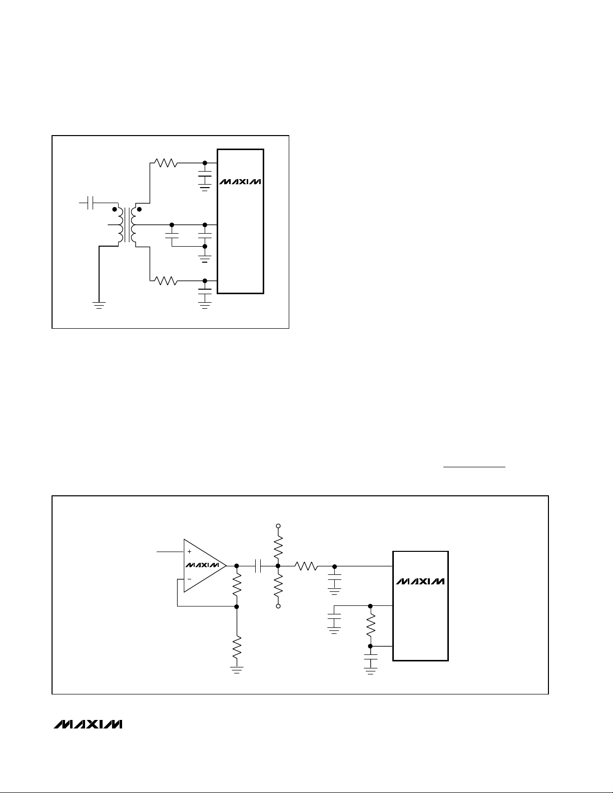
Using Transformer Coupling
An RF transformer (Figure 8) provides an excellent
solution to convert a single-ended source signal to a
fully differential signal, required by the MAX1449 for
optimum performance. Connecting the center tap of the
transformer to COM provides a VDD/2 DC level shift to
the input. Although a 1:1 transformer is shown, a stepup transformer may be selected to reduce the drive
requirements. A reduced signal swing from the input
driver, such as an op amp, may also improve the overall distortion.
In general, the MAX1449 provides better SFDR and
THD with fully differential input signals than singleended drive, especially for very high input frequencies.
In differential input mode, even-order harmonics are
lower as both inputs (IN+, IN-) are balanced, and each
of the inputs only requires half the signal swing compared to single-ended mode.
Single-Ended AC-Coupled Input Signal
Figure 9 shows an AC-coupled, single-ended application. The MAX4108 op amp provides high speed, high
bandwidth, low-noise, and low-distortion to maintain the
integrity of the input signal.
Grounding, Bypassing
and Board Layout
The MAX1449 requires high-speed board layout design
techniques. Locate all bypass capacitors as close to
the device as possible, preferably on the same side as
the ADC, using surface mount devices for minimum
inductance. Bypass VDD, REFP, REFN, and COM with
two parallel 0.1µF ceramic capacitors and a 2.2µF
bipolar capacitor to GND. Follow the same rules to
bypass the digital supply (OVDD) to OGND. Multi-layer
boards with separated ground and power planes produce the highest level of signal integrity. Consider
Figure 5. Output Enable Timing
Figure 6. System and Output Timing Diagram
OE
t
ENABLE
OUTPUT
DATA D9–D0
t
DISABLE
VALID DATA
HIGH-ZHIGH-Z
N
ANALOG INPUT
CLOCK INPUT
t
D0
DATA OUTPUT
N - 6
N - 5
N + 1
5.5 CLOCK-CYCLE LATENCY
N + 2
t
CH
N - 4
N - 3
N + 3
N - 2
N + 4
t
CL
N - 1
N + 5
N
N + 6
N + 1
Page 14

MAX1449
10-Bit, 105Msps, Single +3.3V, Low-Power
ADC with Internal Reference
14 ______________________________________________________________________________________
the use of a split ground plane arranged to match the
physical location of the analog ground (GND) and the
digital output driver ground (OGND) on the ADC's
package. The two ground planes should be joined at a
single point, such that the noisy digital ground currents
do not interfere with the analog ground plane. The ideal
location of this connection can be determined experimentally at a point along the gap between the two
ground planes, which produces optimum results. Make
this connection with a low-value, surface-mount resistor
(1Ω to 5Ω), a ferrite bead or a direct short. Alternatively,
all ground pins could share the same ground plane, if
the ground plane is sufficiently isolated from any noisy
digital systems ground plane (e.g., downstream output
buffer or DSP ground plane). Route high-speed digital
signal traces away from sensitive analog traces. Keep
all signal lines short and free of 90° turns.
Static Parameter Definitions
Integral Nonlinearity (INL)
Integral nonlinearity is the deviation of the values on an
actual transfer function from a straight line. This straight
line can be either a best straight-line fit or a line drawn
between the endpoints of the transfer function, once
offset and gain errors have been nullified. The static linearity parameters for the MAX1449 are measured using
the best straight-line fit method.
Figure 7. Typical Application Circuit Using the Internal Reference
+5V
+5V
INPUT
MAX4108
-5V
0.1µF
0.1µF
300Ω
300Ω
300Ω
300Ω
0.1µF
600Ω
0.1µF
600Ω
MAX4108
-5V
+5V
MAX4108
-5V
600Ω
0.1µF
0.1µF
0.1µF
0.1µF
LOWPASS FILTER
R
ISO
50Ω
LOWPASS FILTER
R
ISO
50Ω
C
IN
22pF
C
IN
22pF
IN+
MAX1449
COM
IN-
300Ω
300Ω
600Ω
Page 15
MAX1449
10-Bit, 105Msps, Single +3.3V, Low-Power
ADC with Internal Reference
______________________________________________________________________________________ 15
Differential Nonlinearity (DNL)
Differential nonlinearity is the difference between an
actual step width and the ideal value of 1LSB. A DNL
error specification of less than 1LSB guarantees no
missing codes and a monotonic transfer function.
Dynamic Parameter Definitions
Aperture Jitter
Figure 10 depicts the aperture jitter (tAJ), which is the
sample-to-sample variation in the aperture delay.
Aperture Delay
Aperture delay (tAD) is the time defined between the
falling-edge of the sampling clock and the instant when
an actual sample is taken (Figure 10).
Signal-to-Noise Ratio (SNR)
For a waveform perfectly reconstructed from digital samples, the theoretical maximum SNR is the ratio of the fullscale analog input (RMS value) to the RMS quantization
error (residual error). The ideal, theoretical minimum analog-to-digital noise is caused by quantization error only
and results directly from the ADC’s resolution (N Bits):
SNR
(MAX)
= (6.02 x N + 1.76)
dB
In reality, there are other noise sources besides quantization noise: thermal noise, reference noise, clock jitter,
etc. SNR is computed by taking the ratio of the RMS
signal to the RMS noise, which includes all spectral
components minus the fundamental, the first five harmonics, and the DC offset.
Signal-to-Noise Plus Distortion (SINAD)
SINAD is computed by taking the ratio of the RMS signal to all spectral components minus the fundamental
and the DC offset.
Effective Number of Bits (ENOB)
ENOB specifies the dynamic performance of an ADC at
a specific input frequency and sampling rate. An ideal
ADC’s error consists of quantization noise only. ENOB
is computed from:
Figure 8. Using a Transformer for AC Coupling
Figure 9. Single-Ended AC-Coupled Input
25Ω
IN+
22pF
0.1µF
V
IN
N.C.
MINICIRCUITS
1
2
T1
TT1–6
6
5
2.2µF
43
0.1µF
25Ω
22pF
MAX1449
COM
IN-
ENOB
SINAD
()
=
.
−
602
.
176
V
IN
MAX4108
R
= 50Ω
ISO
= 22pF
C
IN
100Ω
100Ω
0.1µF
REFP
REFN
1k
R
ISO
IN+
C
1k
0.1µF
IN
MAX1449
COM
R
ISO
C
IN
IN-
Page 16
MAX1449
10-Bit, 105Msps, Single +3.3V, Low-Power
ADC with Internal Reference
16 ______________________________________________________________________________________
Total Harmonic Distortion (THD)
THD is typically the ratio of the RMS sum of the first five
harmonics of the input signal to the fundamental itself.
This is expressed as:
where V1is the fundamental amplitude, and V2through
V5are the amplitudes of the 2nd- through 5th-order
harmonics.
Spurious-Free Dynamic Range (SFDR)
SFDR is the ratio expressed in decibels of the RMS
amplitude of the fundamental (maximum signal component) to the RMS value of the next largest spurious
component, excluding DC offset.
Intermodulation Distortion (IMD)
The two-tone IMD is the ratio expressed in decibels of
either input tone to the worst 3rd-order (or higher) intermodulation products. The individual input tone levels
are at -6.5dB full scale and their envelope is at -0.5dB
full scale.
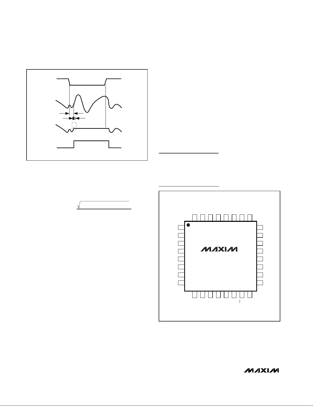
Figure 10. T/H Aperture Timing
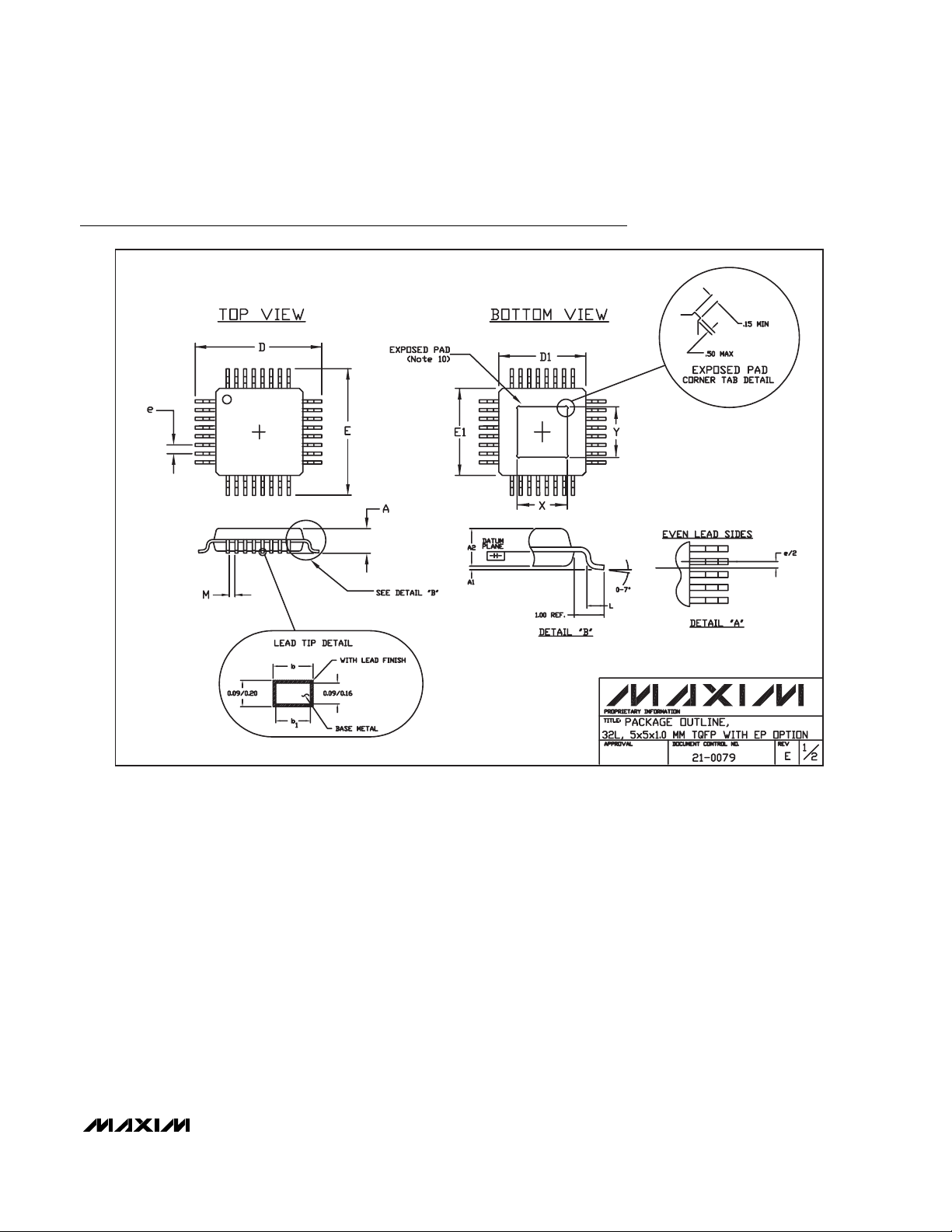
Pin Configuration
Chip Information
TRANSISTOR COUNT: 5684
PROCESS: CMOS
MAX1449
TQFP
TOP VIEW
32 28
293031
25
26
27
REFIN
GND
REFOUT
D0
REFP
D1
D2
D3
10
13
15
14
1611 12
9
V
DD
GND
V
DD
PD
CLK
OE
GND
D9
17
18
19
20
21
22
23
OGND
24 D4
T.P.
OV
DD
D5
D6
D7
D8
2
3
4
5
6
7
8GND
IN-
IN+
GND
GND
V
DD
COM
1REFN
CLK
ANALOG
INPUT
t
AD
SAMPLED
DATA (T/H)
T/H
TRACK TRACK
t
AJ
HOLD
20
THD
=×
log
2
2
2
VVVV
+++
()
2
3
4
V
1
2
5
Page 17
MAX1449
10-Bit, 105Msps, Single +3.3V, Low-Power
ADC with Internal Reference
______________________________________________________________________________________ 17
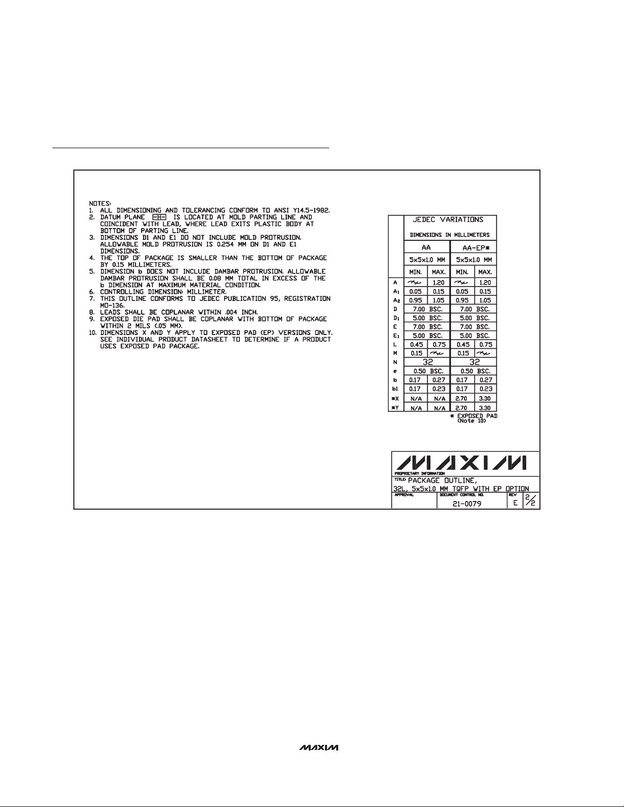
Package Information
32L,TQFP.EPS
Page 18
MAX1449
10-Bit, 80Msps, Single +3.3V, Low-Power
ADC with Internal Reference
Maxim cannot assume responsibility for use of any circuitry other than circuitry entirely embodied in a Maxim product. No circuit patent licenses are
implied. Maxim reserves the right to change the circuitry and specifications without notice at any time.
18 ____________________Maxim Integrated Products, 120 San Gabriel Drive, Sunnyvale, CA 94086 408-737-7600
© 2000 Maxim Integrated Products Printed USA is a registered trademark of Maxim Integrated Products.
Package Information (continued)
 Loading...