

Page 1
General Description
The MAX1427 is a 5V, high-speed, high-performance
analog-to-digital converter (ADC) featuring a fully differential wideband track-and-hold (T/H) and a 15-bit converter core. The MAX1427 is optimized for multichannel,
multimode receivers, which require the ADC to meet very
stringent dynamic performance requirements. With a
noise floor of -79.3dBFS, the MAX1427 allows for the
design of receivers with superior sensitivity.
The MAX1427 achieves two-tone, spurious-free dynamic
range (SFDR) of -91dBc for input tones of 10MHz and
15MHz. Its excellent signal-to-noise ratio (SNR) of 76.1dB
and single-tone SFDR performance (SFDR1/SFDR2) of
93.5dBc/94.5dBc at f
IN
= 15MHz and a sampling rate of
80Msps make this part ideal for high-performance digital
receivers.
The MAX1427 operates from an analog 5V and a digital
3V supply, features a 2.56V
P-P
full-scale input range,
and allows for a sampling speed of up to 80Msps. The
input T/H operates with a -1dB full-power bandwidth of
200MHz.
The MAX1427 features parallel, CMOS-compatible outputs in two’s-complement format. To enable the interface
with a wide range of logic devices, this ADC provides a
separate output driver power-supply range of 2.3V to
3.5V. The MAX1427 is manufactured in an 8mm x 8mm,
56-pin thin QFN package with exposed paddle (EP) for
low thermal resistance, and is specified for the extended
industrial (-40°C to +85°C) temperature range.
Note that IF parts MAX1418, MAX1428, and MAX1430
(see Pin-Compatible Higher/Lower Speed Versions
Selection table) are recommended for applications that
require high dynamic performance for input frequencies greater than f
CLK
/3. The MAX1427 is optimized for
input frequencies of less than f
CLK
/3.
Applications
Cellular Base-Station Transceiver Systems (BTS)
Wireless Local Loop (WLL)
Single- and Multicarrier Receivers
Multistandard Receivers
E911 Location Receivers
Power Amplifier Linearity Correction
Antenna Array Processing
Features
♦ 80Msps Minimum Sampling Rate
♦ -79.3dBFS Noise Floor
♦ Excellent Dynamic Performance
76.1dB SNR at f
IN
= 15MHz and A
IN
= -1dBFS
93.5dBc/94.5dBc Single-Tone SFDR1/SFDR2 at
f
IN
= 15MHz and A
IN
= -1dBFS
-91dBc Multitone SFDR at f
IN1
= 10MHz
and f
IN2
= 15MHz
♦ Less than 0.25ps Sampling Jitter
♦ Fully Differential Analog Input Voltage Range of
2.56V
P-P
♦ CMOS-Compatible Two’s-Complement Data Output
♦ Separate Data Valid Clock and Overrange Outputs
♦ Flexible-Input Clock Buffer
♦ EV Kit Available for MAX1427
(Order MAX1427EVKIT)
MAX1427
15-Bit, 80Msps ADC with -79.3dBFS
Noise Floor for Baseband Applications
________________________________________________________________ Maxim Integrated Products 1
Ordering Information
19-3010; Rev 1; 2/04
For pricing, delivery, and ordering information, please contact Maxim/Dallas Direct! at
1-888-629-4642, or visit Maxim’s website at www.maxim-ic.com.
EVALUATION KIT
AVAILABLE
Pin Configuration appears at end of data sheet.
PART TEMP RANGE PIN-PACKAGE
MAX1427ETN -40°C to +85°C 56 Thin QFN-EP*
Pin-Compatible Higher/Lower
Speed Versions Selection
PART
SPEED GRADE
(Msps)
TARGET
APPLICATION
MAX1418 65 IF
MAX1419 65 Baseband
MAX1427 80 Baseband
MAX1428* 80 IF
MAX1429* 100 Baseband
MAX1430* 100 IF
*
Future product—contact factory for availability.
*
EP = Exposed paddle.
Page 2
MAX1427
15-Bit, 80Msps ADC with -79.3dBFS
Noise Floor for Baseband Applications
2 _______________________________________________________________________________________
ABSOLUTE MAXIMUM RATINGS
ELECTRICAL CHARACTERISTICS
(AVCC= 5V, DVCC= DRVCC= 2.5V, GND = 0, INP and INN driven differentially with -1dBFS, CLKP and CLKN driven differentially
with a 2V
P-P
sinusoidal input signal, CL= 5pF at digital outputs, f
CLK
= 80MHz, TA= T
MIN
to T
MAX
, unless otherwise noted. Typical
values are at T
A
= +25°C, unless otherwise noted. ≥+25°C guaranteed by production test, <+25°C guaranteed by design and char-
acterization.)
Stresses beyond those listed under “Absolute Maximum Ratings” may cause permanent damage to the device. These are stress ratings only, and functional
operation of the device at these or any other conditions beyond those indicated in the operational sections of the specifications is not implied. Exposure to
absolute maximum rating conditions for extended periods may affect device reliability.
AVCC, DVCC, DRVCCto GND.................................. -0.3V to +6V
INP, INN, CLKP, CLKN, CM to GND........-0.3V to (AV
CC
+ 0.3V)
D0–D14, DAV, DOR to GND..................-0.3V to (DRV
CC
+ 0.3V)
Continuous Power Dissipation (T
A
= +70°C)
56-Pin Thin QFN (derate 47.6mW/°C above +70°C)................
3809.5mW
Operating Temperature Range ...........................-40°C to +85°C
Thermal Resistance
θ
J
A
...................................................21°C/W
Junction Temperature......................................................+150°C
Storage Temperature Range .............................-60°C to +150°C
PARAMETER
SYMBOL
CONDITIONS
MIN
TYP
MAX
UNITS
DC ACCURACY
Resolution 15 Bits
Integral Nonlinearity INL f
IN
= 15MHz
LSB
Differential Nonlinearity DNL f
IN
= 15MHz, no missing codes guaranteed
LSB
Offset Error -12
mV
Gain Error -4 +4
%FS
ANALOG INPUT (INP, INN)
D i ffer enti al Inp ut V ol tag e Rang e
V
DIFF
V
P-P
Common-Mode Input Voltage
V
CM
Self-biased
V
Differential Input Resistance R
IN
1
kΩ
Differential Input Capacitance
C
IN
1pF
Full-Power Analog Bandwidth
-1dB rolloff for a full-scale input
MHz
CONVERSION RATE
Maximum Clock Frequency f
CLK
80
MHz
Minimum Clock Frequency f
CLK
20
MHz
Aperture Jitter t
AJ
ps
RMS
CLOCK INPUT (CLKP, CLKN)
Full-Scale Differential Input
Voltage
0.5 to
3.0
V
Common-Mode Input Voltage
V
CM
Self-biased 2.4 V
Differential Input Resistance R
INCLK
2
kΩ
Differential Input Capacitance
C
INCLK
1pF
DYNAMIC CHARACTERISTICS
Thermal + Quantization
Noise Floor
NF Analog input <-35dBFS
dBFS
fIN = 5MHz at -1dBFS
fIN = 15MHz at -1dBFS
Signal-to-Noise Ratio (Note 1)
SNR
f
IN
= 35MHz at -1dBFS
dB
Fully differential inputs drive, V
FPBW
-1dB
V
DIFFCLK
DIFF
= V
INP
±1.5
±0.4
- V
INN
73.5 76.1
2.56
3.38
±15%
200
0.21
±15%
-79.3
76.5
75.6
+12
Page 3
MAX1427
15-Bit, 80Msps ADC with -79.3dBFS
Noise Floor for Baseband Applications
_______________________________________________________________________________________ 3
ELECTRICAL CHARACTERISTICS (continued)
(AVCC= 5V, DVCC= DRVCC= 2.5V, GND = 0, INP and INN driven differentially with -1dBFS, CLKP and CLKN driven differentially
with a 2V
P-P
sinusoidal input signal, CL= 5pF at digital outputs, f
CLK
= 80MHz, TA= T
MIN
to T
MAX
, unless otherwise noted. Typical
values are at T
A
= +25°C, unless otherwise noted. ≥+25°C guaranteed by production test, <+25°C guaranteed by design and char-
acterization.)
PARAMETER
SYMBOL
CONDITIONS
MIN
TYP
MAX
UNITS
fIN = 5MHz at -1dBFS
fIN = 15MHz at -1dBFS 73
Signal-to-Noise and Distortion
(Note 1)
f
IN
= 35MHz at -1dBFS
dB
fIN = 5MHz at -1dBFS
fIN = 15MHz at -1dBFS 84
Spurious-Free Dynamic Range
(HD2 and HD3)
(Note 1)
SFDR1
f
IN
= 35MHz at -1dBFS 85
dBc
fIN = 5MHz at -1dBFS
fIN = 15MHz at -1dBFS
Spurious-Free Dynamic Range
(HD4 and Higher)
(Note 1)
SFDR2
f
IN
= 35MHz at -1dBFS 91
dBc
Two-Tone Intermodulation
Distortion
TTIMD
f
IN1
= 10MHz at -7dBFS;
f
IN2
= 15MHz at -7dBFS
dBc
Two-Tone Spurious-Free
Dynamic Range
f
IN1
= 10MHz at -10dBFS < f
IN1
< -100dBFS;
f
IN2
= 15MHz at -10dBFS < f
IN2
< -100dBFS
dBFS
DIGITAL OUTPUTS (D0–D14, DAV, DOR)
Digital Output Voltage Low V
OL
0.5 V
Digital Output Voltage High V
OH
DVCC -
0.5
V
TIMING CHARACTERISTICS (DV
CC
= DRV
CC
= 2.5V) Figure 4
CLKP/CLKN Duty Cycle
50
±5
%
Effective Aperture Delay t
AD
ps
Output Data Delay t
DAT
(Note 3) 3 4.5 7.5 ns
Data Valid Delay t
DAV
(Note 3) 5.3 6.5 8.7 ns
Pipeline Latency
3
Clock
cycles
CLKP Rising Edge to DATA
Not Valid
t
DNV
(Note 3) 2.6 3.8 5.7 ns
CLKP Rising Edge to DATA
Valid (Guaranteed)
t
DGV
(Note 3) 3.4 5.2 8.6 ns
DATA Setup Time
(Before DAV Rising Edge)
t
SETUP
(Note 3)
t
CLKP
-
0.5
t
CLKP
t
CLKP
ns
DATA Hold Time
(After DAV Rising Edge)
t
HOLD
(Note 3)
t
CLKN
-
3.6
t
CLKN
-
2.8
t
CLKN
-
2.0
ns
76.3
75.9
75.3
96.5
93.5
94.5
85.5 94.5
-91
SFDR
TT
-105
Duty cycle
t
LATENCY
230
+ 1.3
+ 2.4
Page 4
MAX1427
15-Bit, 80Msps ADC with -79.3dBFS
Noise Floor for Baseband Applications
4 _______________________________________________________________________________________
Note 1: Dynamic performance is based on a 32,768-point data record with a sampling frequency of f
SAMPLE
= 80.019456MHz, an
input frequency of f
IN
= f
SAMPLE
x (6143/32768) = 15.001206MHz, and a frequency bin size of 2442Hz. Close-in (f
IN
±29.3kHz) and low-frequency (DC to 58.6kHz) bins are excluded from the spectrum analysis.
Note 2: Apply the same voltage levels to DV
CC
and DRVCC.
Note 3: Guaranteed by design and characterization.
ELECTRICAL CHARACTERISTICS (continued)
(AVCC= 5V, DVCC= DRVCC= 2.5V, GND = 0, INP and INN driven differentially with -1dBFS, CLKP and CLKN driven differentially
with a 2V
P-P
sinusoidal input signal, CL= 5pF at digital outputs, f
CLK
= 80MHz, TA= T
MIN
to T
MAX
, unless otherwise noted. Typical
values are at T
A
= +25°C, unless otherwise noted. ≥+25°C guaranteed by production test, <+25°C guaranteed by design and char-
acterization.)
PARAMETER
SYMBOL
CONDITIONS
MIN
TYP
MAX
UNITS
TIMING CHARACTERISTICS (DV
CC
= DRV
CC
= 3.3V) Figure 4
CLKP/CLKN Duty Cycle
50
±5
%
Effective Aperture Delay t
AD
ps
Output Data Delay t
DAT
(Note 3) 2.8 4.1 6.5 ns
Data Valid Delay t
DAV
(Note 3) 5.3 6.3 8.6 ns
Pipeline Latency
3
Clock
cycles
CLKP Rising Edge to
DATA Not Valid
t
DNV
(Note 3) 2.5 3.4 5.2 ns
CLKP Rising Edge to
DATA Valid (Guaranteed)
t
DGV
(Note 3) 3.2 4.4 7.4 ns
DATA Setup Time
(Before DAV Rising Edge)
t
SETUP
(Note 3)
t
CLKP
t
CLKP
t
CLKP
ns
DATA Hold Time
(After DAV Rising Edge)
t
HOLD
(Note 3)
t
CLKN
-
3.5
t
CLKN
-
2.7
t
CLKN
-
2.0
ns
POWER REQUIREMENTS
Analog Supply Voltage Range
AV
CC
V
Digital Supply Voltage Range
DV
CC
(Note 2)
V
Output Supply Voltage Range
DRV
CC
(Note 2)
V
Analog Supply Current I
AVCC
mA
D i g i tal + Outp ut S up p l y C ur r ent
I
DVCC
+
f
CLK
= 80MHz, C
LOAD
= 5pF
42 mA
Analog Power Dissipation PDISS
mW
Duty cycle
t
LATENCY
+ 0.2
230
+ 1.7
+ 2.8
5 ±3%
2.3 to 3.5
2.3 to 3.5
377 440
35.5
1974
Page 5
MAX1427
15-Bit, 80Msps ADC with -79.3dBFS
Noise Floor for Baseband Applications
_______________________________________________________________________________________ 5
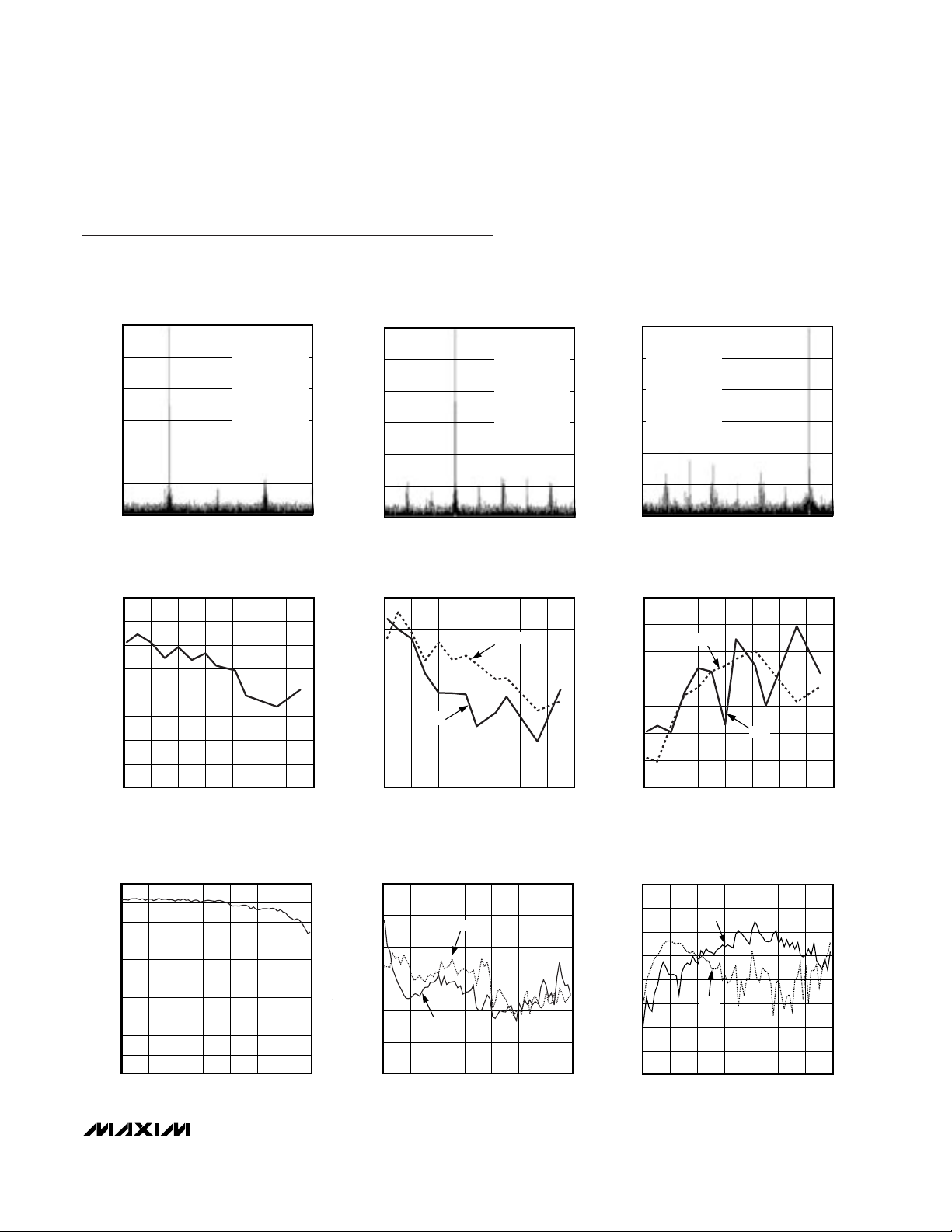
FFT PLOT (32,768-POINT DATA RECORD,
COHERENT SAMPLING)
MAX1427 toc01
ANALOG INPUT FREQUENCY (MHz)
AMPLITUDE (dBFS)
252015105
-100
-80
-60
-40
-20
0
-120
0403530
f
CLK
= 80.0195MHz
f
IN
= 9.9999MHz
A
IN
= -1.04dBFS
SNR = 76.3dB
SFDR1 = 96.2dBc
SFDR2 = 98.91dBc
HD2 = -102.5dBc
HD3 = -96.2dBc
FFT PLOT (32,768-POINT DATA RECORD,
COHERENT SAMPLING)
MAX1427 toc02
ANALOG INPUT FREQUENCY (MHz)
AMPLITUDE (dBFS)
252015105
-100
-80
-60
-40
-20
0
-120
0403530
f
CLK
= 80.0195MHz
f
IN
= 15.0012MHz
A
IN
= -1.00dBFS
SNR = 76dB
SFDR1 = 94.7dBc
SFDR2 = 94.7dBc
HD2 = -94.7dBc
HD3 = -104.8dBc
FFT PLOT (32,768-POINT DATA RECORD,
COHERENT SAMPLING)
MAX1427 toc03
ANALOG INPUT FREQUENCY (MHz)
AMPLITUDE (dBFS)
252015105
-100
-80
-60
-40
-20
0
-120
0403530
f
CLK
= 80.0195MHz
f
IN
= 35.0012MHz
A
IN
= -1.02dBFS
SNR = 75.5dB
SFDR1 = 84.4dBc
SFDR2 = 87dBc
HD2 = -84.4dBc
HD3 = -91.6dBc
SNR vs. ANALOG INPUT FREQUENCY
(f
CLK
= 80.0195MHz, AIN = -1dBFS)
MAX1427 toc04
fIN (MHz)
SNR (dB)
554515 25 35
71
72
73
74
75
76
77
78
70
5757065
SFDR1/SFDR2 vs. ANALOG INPUT FREQUENCY
(f
CLK
= 80.0195MHz, AIN = -1dBFS)
MAX1427 toc05
fIN (MHz)
SFDR1/SFDR2 (dBc)
5545352515
75
80
85
90
95
100
70
5757065
SFDR2
SFDR1
HD2/HD3 vs. ANALOG INPUT FREQUENCY
(f
CLK
= 80.0195MHz, AIN = -1dBFS)
MAX1427 toc06
fIN (MHz)
HD2/HD3 (dBc)
5545352515
-100
-95
-90
-85
-80
-75
-110
-105
5757065
HD2
HD3
FULL-SCALE-TO-NOISE RATIO
vs. ANALOG INPUT AMPLITUDE
(f
CLK
= 80.0195MHz, fIN = 15.0012MHz)
MAX1427 toc07
ANALOG INPUT AMPLITUDE (dBFS)
FULL-SCALE-TO-NOISE RATIO (dBFS)
-10-20-40 -30-50-60
71
72
73
74
75
76
77
78
79
80
70
-70 0
SFDR1/SFDR2 vs. ANALOG INPUT AMPLITUDE
(f
CLK
= 80.0195MHz, fIN = 15.0012MHz)
MAX1427 toc08
ANALOG INPUT AMPLITUDE (dBFS)
SFDR1/SFDR2 (dBFS)
-10-20-40 -30-50-60
80
90
100
110
120
130
70
-70 0
SFDR1
SFDR2
HD2/HD3 vs. ANALOG INPUT AMPLITUDE
(f
CLK
= 80.195MHz, fIN = 15.00102MHz)
MAX1427 toc09
ANALOG INPUT AMPLITUDE (dBFS)
HD2/HD3 (dBFS)
-10-20-40 -30-50-60
-120
-110
-100
-90
-80
-70
-150
-140
-130
-70 0
HD2
HD3
Typical Operating Characteristics
(AV
CC
= 5V, DV
CC
= DRV
CC
= 2.5V, INP and INN driven differentially with a -1dBFS amplitude, CLKP and CLKN driven differentially
with a 2V
P-P
sinusoidal input signal, CL= 5pF at digital outputs, f
CLK
= 80MHz, TA= +25°C. All AC data based on a 32k-point FFT
record and under coherent sampling conditions.)
Page 6
MAX1427
15-Bit, 80Msps ADC with -79.3dBFS
Noise Floor for Baseband Applications
6 _______________________________________________________________________________________
SNR vs. SAMPLING FREQUENCY
(f
IN
= 15.2MHz, AIN = -1dBFS)
MAX1427 toc10
f
CLK
(MHz)
SNR (dB)
30 40 50 7060 80
71
72
73
74
75
76
77
78
20
SFDR1/SFDR2 vs. SAMPLING FREQUENCY
(f
IN
= 15.2MHz, AIN = -1dBFS)
MAX1427 toc11
f
CLK
(MHz)
SFDR1/SFDR2 (dBc)
807060504030
75
80
85
90
95
100
70
20
SFDR1
SFDR2
HD2/HD3 vs. SAMPLING FREQUENCY
(f
IN
= 15.2MHz, AIN = -1dBFS)
MAX1427 toc12
f
CLK
(MHz)
HD2/HD3 (dBc)
705030 40
-115
-110
-105
-100
-95
-90
-85
-80
-75
-70
-120
20 8060
HD3
HD2
SNR vs. TEMPERATURE
(f
CLK
= 80.0195MHz,
f
IN
= 15.0012MHz, AIN = -1dBFS)
MAX1427 toc13
TEMPERATURE (°C)
SNR (dB)
603510-15
74
75
76
77
78
73
-40 85
SINAD vs. TEMPERATURE
(f
CLK
= 80.0195MHz,
f
IN
= 15.0012MHz, AIN = -1dBFS)
MAX1427 toc14
TEMPERATURE (°C)
SINAD (dB)
603510-15
74
75
76
77
78
71
72
73
-40 85
Typical Operating Characteristics (continued)
(AV
CC
= 5V, DV
CC
= DRV
CC
= 2.5V, INP and INN driven differentially with a -1dBFS amplitude, CLKP and CLKN driven differentially
with a 2V
P-P
sinusoidal input signal, CL= 5pF at digital outputs, f
CLK
= 80MHz, TA= +25°C. All AC data based on a 32k-point FFT
record and under coherent sampling conditions.)
Page 7

MAX1427
15-Bit, 80Msps ADC with -79.3dBFS
Noise Floor for Baseband Applications
_______________________________________________________________________________________ 7
TWO-TONE IMD PLOT (32,768-POINT
DATA RECORD, COHERENT SAMPLING)
MAX1427 toc19
ANALOG INPUT FREQUENCY (MHz)
AMPLITUDE (dBFS)
252015105
-100
-80
-60
-40
-20
0
-120
03530 40
f
CLK
= 80.0195MHz
f
IN1
= 10.0010MHz
f
IN2
= 15.0010MHz
A
IN1
= A
IN2
= -7dBFS
2f
IN1
- f
IN2
2f
IN2
- f
IN1
f
IN1
f
IN2
SFDR1/SFDR2 vs. TEMPERATURE
(f
CLK
= 80.0195MHz,
f
IN
= 15.0012MHz, AIN = -1dBFS)
MAX1427 toc15
TEMPERATURE (°C)
SFDR1/SFDR2 (dBc)
603510-15
80
85
90
95
100
75
-40 85
SFDR1
SFDR2
HD2/HD3 vs. TEMPERATURE
(f
CLK
= 80.0195MHz,
f
IN
= 15.0012MHz, AIN = -1dBFS)
MAX1427 toc16
TEMPERATURE (°C)
HD2/HD3 (dBc)
603510-15
-100
-95
-90
-85
-80
-110
-105
-40 85
HD2
HD3
POWER DISSIPATION vs. TEMPERATURE
(f
CLK
= 80.0195MHz,
f
IN
= 15.0012MHz, AIN = -1dBFS)
MAX1427 toc17
TEMPERATURE (°C)
POWER DISSIPATION (mW)
603510-15
1969
1973
1977
1981
1985
1965
-40 85
POWER DISSIPATION vs. SUPPLY VOLTAGE
(f
CLK
= 80.0195MHz,
f
IN
= 15.0012MHz, AIN = -1dBFS)
MAX1427 toc18
SUPPLY VOLTAGE (V)
POWER DISSIPATION (mW)
5.205.154.90 4.95 5.00 5.05 5.10
1850
1900
1950
2000
2050
2100
2150
2200
1800
4.85 5.25
Typical Operating Characteristics (continued)
(AV
CC
= 5V, DV
CC
= DRV
CC
= 2.5V, INP and INN driven differentially with a -1dBFS amplitude, CLKP and CLKN driven differentially
with a 2V
P-P
sinusoidal input signal, CL= 5pF at digital outputs, f
CLK
= 80MHz, TA= +25°C. All AC data based on a 32k-point FFT
record and under coherent sampling conditions.)
Page 8

MAX1427
15-Bit, 80Msps ADC with -79.3dBFS
Noise Floor for Baseband Applications
8 _______________________________________________________________________________________
Pin Description
PIN NAME FUNCTION
1, 2, 3, 6, 9, 12, 14–17,
20, 23, 26, 27, 30, 52–56, EP
GND
Converter Ground. Analog, digital, and output driver grounds are internally
connected to the same potential. Connect the converter’s EP to GND.
4 CLKP Differential Clock, Positive Input Terminal
5 CLKN Differential Clock, Negative Input Terminal
7, 8, 18, 19, 21, 22, 24, 25, 28
AV
CC
Analog Supply Voltage. Provide local bypassing to ground with 0.1µF to 0.22µF
capacitors.
10 INP Differential Analog Input, Positive Terminal
11 INN Differential Analog Input, Negative/Complementary Terminal
13 CM Common-Mode Reference Terminal
29 DV
CC
Digital Supply Voltage. Provide local bypassing to ground with 0.1µF to 0.22µF
capacitors.
31, 41, 42, 51 DRV
CC
Digital Output Driver Supply Voltage. Provide local bypassing to ground with
0.1µF to 0.22µF capacitors.
32 DOR
Data Overrange Bit. This control line flags an overrange condition in the ADC.
If DOR transitions high, an overrange condition is detected. If DOR remains low, the
ADC operates within the allowable full-scale range.
33 D0 Digital CMOS Output Bit 0 (LSB)
34 D1 Digital CMOS Output Bit 1
35 D2 Digital CMOS Output Bit 2
36 D3 Digital CMOS Output Bit 3
37 D4 Digital CMOS Output Bit 4
38 D5 Digital CMOS Output Bit 5
39 D6 Digital CMOS Output Bit 6
40 D7 Digital CMOS Output Bit 7
43 D8 Digital CMOS Output Bit 8
44 D9 Digital CMOS Output Bit 9
45 D10 Digital CMOS Output Bit 10
46 D11 Digital CMOS Output Bit 11
47 D12 Digital CMOS Output Bit 12
48 D13 Digital CMOS Output Bit 13
49 D14 Digital CMOS Output Bit 14 (MSB)
50 DAV
Data Valid Output. This output can be used as a clock control line to drive an
external buffer or data-acquisition system. The typical delay time between the
falling edge of the converter clock and the rising edge of DAV is 6.5ns.
Page 9

MAX1427
15-Bit, 80Msps ADC with -79.3dBFS
Noise Floor for Baseband Applications
_______________________________________________________________________________________ 9
Detailed Description
Figure 1 provides an overview of the MAX1427 architecture. The MAX1427 employs an input T/H amplifier,
which has been optimized for low thermal noise and
low distortion. The high-impedance differential inputs to
the T/H amplifier (INP and INN) are self-biased at
3.38V, and support a full-scale differential input voltage
of 2.56V
P-P
. The output of the T/H amplifier is fed to a
multistage pipelined ADC core, which has also been
optimized to achieve a very low thermal noise floor and
low distortion.
A clock buffer receives a differential input clock waveform and generates a low-jitter clock signal for the input
T/H. The signal at the analog inputs is sampled at the
rising edge of the differential clock waveform. The differential clock inputs (CLKP and CLKN) are highimpedance inputs, are self-biased at 2.4V, and support
differential clock waveforms from 0.5V
P-P
to 3.0V
P-P
.
The outputs from the multistage pipelined ADC core
are delivered to error correction and formatting logic,
which in turn, deliver the 15-bit output code in two’scomplement format to digital output drivers. The output
drivers provide CMOS-compatible outputs with levels
programmable over a 2.3V to 3.5V range.
Analog Inputs and
Common Mode (INP, INN, CM)
The signal inputs to the MAX1427 (INP and INN) are
balanced differential inputs. This differential configuration provides immunity to common-mode noise coupling
and rejection of even-order harmonic terms. The differential signal inputs to the MAX1427 should be AC-coupled and carefully balanced in order to achieve the best
dynamic performance (see the Applications Information
section for more detail). AC-coupling of the input signal
is easily accomplished because the MAX1427 inputs
are self-biasing as illustrated in Figure 2. Although the
T/H inputs are high impedance, the actual differential
input impedance is nominally 1kΩ because of the two
500Ω bias resistors connected from each input to the
common-mode reference.
The CM pin provides a monitor of the input commonmode self-bias potential. In most applications, in which
the input signal is AC-coupled, this pin is not connected. If DC-coupling of the input signal is required, this
pin may be used to construct a DC servo loop to control the input common-mode potential. See the
Applications Information section for more details.
T/H
CORRECTION
LOGIC + OUTPUT
BUFFERS
INTERNAL
TIMING
INTERNAL
REFERENCE
INP
INN
CM
CLKP
CLKN
DAV
15
DATA BITS D0 THROUGH D14
AV
CC
DRV
CC
DV
CC
GND
MULTISTAGE
PIPELINE ADC CORE
CLOCK
BUFFER
MAX1427
Figure 1. Simplified MAX1427 Block Diagram
BUFFER
INTERNAL REFERENCE
AND BIASING CIRCUIT
T/H AMPLIFIER
T/H AMPLIFIER
500Ω
500Ω
CM
INP
INN
TO 1. QUANTIZER STAGE
TO 1. QUANTIZER STAGE
1kΩ
Figure 2. Simplified Analog and Common-Mode Input Architecture
Page 10

MAX1427
15-Bit, 80Msps ADC with -79.3dBFS
Noise Floor for Baseband Applications
10 ______________________________________________________________________________________
On-Chip Reference Circuit
The MAX1427 incorporates an on-chip 2.5V, low-drift
bandgap reference. This reference potential establishes the full-scale range for the converter, which is nominally 2.56V
P-P
differential. The internal reference
potential is not accessible to the user, so the full-scale
range for the MAX1427 cannot be externally adjusted.
Figure 3 shows how the reference is used to generate
the common-mode bias potential for the analog inputs.
The common-mode input bias is set to one diode
potential above the bandgap reference potential, and
so varies over temperature.
Clock Inputs (CLKP, CLKN)
The differential clock buffer for the MAX1427 has been
designed to accept an AC-coupled clock waveform.
Like the signal inputs, the clock inputs are self-biasing.
In this case, the common-mode bias potential is 2.4V
and each input is connected to the reference potential
through a 1kΩ resistor. Consequently, the differential
input resistance associated with the clock inputs is
2kΩ. While differential clock signals as low as 0.5V
P-P
may be used to drive the clock inputs, best dynamic
performance is achieved with clock input voltage levels
of 2V
P-P
to 3V
P-P
. Jitter on the clock signal translates
directly to jitter (noise) on the sampled signal.
Therefore, the clock source should be a low-jitter (lowphase noise) source. See the Applications Information
section for additional details on driving the clock inputs.
System Timing Requirements
Figure 4 depicts the timing relationships for the signal
input, clock input, data output, and DAV output. The
variables shown in the figure correspond to the various
timing specifications in the Electrical Characteristics
section. These include:
• t
DAT
: Delay from the rising edge of the clock until the
50% point of the output data transition
• t
DAV
: Delay from the falling edge of the clock until the
50% point of the DAV rising edge
• t
DNV
: Time from the rising edge of the clock until data
is no longer valid
1mA
2mA
INP/INN
COMMON-MODE
REFERENCE
500Ω 500Ω
1kΩ
2.5V
Figure 3. Simplified Reference Architecture
INP
INN
D0–D14
DOR
DAV
N + 1NN + 2N + 3
CLKP
CLKN
t
AD
t
CLKP
t
CLKN
N - 3 N - 2 N - 1 N
t
S
t
H
t
DAT
t
DAV
t
DNV
t
DGV
Figure 4. System and Output Timing Diagram
Page 11

MAX1427
15-Bit, 80Msps ADC with -79.3dBFS
Noise Floor for Baseband Applications
______________________________________________________________________________________ 11
• t
DGV
: Time from the rising edge of the clock until data
is guaranteed to be valid
• t
SETUP
: Time from data guaranteed valid until the ris-
ing edge of DAV
• t
HOLD
: Time from the rising edge of DAV until data is
no longer valid
• t
CLKP
: Time from the 50% point of the rising edge to
the 50% point of the falling edge of the clock signal
• t
CLKN
: Time from 50% point of the falling edge to the
50% point of the rising edge of the clock signal
The MAX1427 samples the input signal on the rising
edge of the input clock. Output data is valid on the rising edge of the DAV signal, with a data latency of three
clock cycles. Note that the clock duty cycle must be
50% ±5% for proper operation.
Digital Outputs (D0–D14, DAV, DOR)
The logic “high” level of the CMOS-compatible digital
outputs (D0–D14, DAV, and DOR) may be set in the
2.3V to 3.5V range. This is accomplished by setting the
voltage at the DVCCand DRVCCpins to the desired
logic-high level. Note that the DV
CC
and DRVCCvolt-
ages must be the same value.
For best performance, the capacitive loading on the digital
outputs of the MAX1427 should be kept as low as possible
(<10pF). Large capacitive loads result in large charging
currents during data transitions, which may feed back into
the analog section of the ADC and create distortion terms.
The loading capacitance is kept low by keeping the output
traces short and by driving a single CMOS buffer or latch
input (as opposed to multiple CMOS inputs).
Inserting small series resistors (220Ω or less) between
the MAX1427 outputs and the digital load, placed as
closely as possible to the output pins, is helpful in controlling the size of the charging currents during data
transitions and can improve dynamic performance.
Keep the trace length from the resistor to the load as
short as possible to minimize trace capacitance.
The output data is in two’s complement format, as illustrated in Table 1.
Data is valid at the rising edge of DAV (Figure 4), and
DAV may be used as a clock signal to latch the output
data. The DAV output provides twice the drive strength
of the data outputs, and may therefore be used to drive
multiple data latches.
The DOR output is used to identify an overrange condition. If the input signal exceeds the positive or negative
full-scale range for the MAX1427, then DOR is asserted
high. The timing for DOR is identical to the timing for
the data outputs, and DOR therefore provides an overrange indication on a sample-by-sample basis.
Table 1. MAX1419 Digital Output Coding
INP
ANALOG VOLTAGE LEVEL
INN
ANALOG VOLTAGE LEVEL
D14–D0
TWO’S COMPLEMENT CODE
V
REF
+ 0.64V V
REF
- 0.64V
0 1 1 1 1 1 1 1 1 1 1 1 1 1 1
(positive full scale)
V
REF
V
REF
0 0 0 0 0 0 0 0 0 0 0 0 0 0 0
(midscale + δ)
1 1 1 1 1 1 1 1 1 1 1 1 1 1 1
(midscale - δ)
V
REF
- 0.64V V
REF
+ 0.64V
1 0 0 0 0 0 0 0 0 0 0 0 0 0 0
(negative full scale)
Page 12

MAX1427
15-Bit, 80Msps ADC with -79.3dBFS
Noise Floor for Baseband Applications
12 ______________________________________________________________________________________
Applications Information
Differential, AC-Coupled Clock Input
The clock inputs to the MAX1427 are designed to be
driven with an AC-coupled differential signal, and best
performance is achieved under these conditions.
However, it is often the case that the available clock
source is single ended. Figure 5 demonstrates one
method for converting a single-ended clock signal into
a differential signal through a transformer. In this example, the transformer turns ratio from the primary to secondary side is 1:1.414. The impedance ratio from
primary to secondary is the square of the turns ratio, or
1:2, so that terminating the secondary side with a 100Ω
differential resistance results in a 50Ω load looking into
the primary side of the transformer. The termination
resistor in this example comprises the series combination of two 50Ω resistors with their common node ACcoupled to ground. Alternatively, a single 100Ω resistor
across the two inputs with no common-mode connection could be employed.
In the example of Figure 5, the secondary side of the
transformer is coupled directly to the clock inputs.
Since the clock inputs are self-biasing, the center tap of
the transformer must be AC-coupled to ground or left
floating. If the center tap of the secondary were DCcoupled to ground, then it would be necessary to add
blocking capacitors in series with the clock inputs.
Clock jitter is generally improved if the clock signal has
a high slew rate at the time of its zero crossing.
Therefore, if a sinusoidal source is used to drive the
clock inputs, it is desirable that the clock amplitude be
as large as possible to maximize the zero-crossing
slew rate. The back-to-back Schottky diodes shown in
Figure 5 are not required as long as the input signal is
held to 3V
P-P
differential or less. If a larger amplitude
signal is provided (to maximize the zero-crossing slew
rate), then the diodes serve to limit the differential signal swing at the clock inputs.
Any differential mode noise coupled to the clock inputs
translates to clock jitter and degrades the SNR performance of the MAX1427. Any differential mode coupling
of the analog input signal into the clock inputs results in
harmonic distortion. Consequently, it is important that
the clock lines be well isolated from the analog signal
input and from the digital outputs. See the PC Board
Layout Considerations sections for more discussion on
noise coupling.
Differential, AC-Coupled Analog Input
The analog inputs (INP and INN) are designed to be driven with a differential AC-coupled signal. It is extremely
important that these inputs be accurately balanced. Any
common-mode signal applied to these inputs degrade
even-order distortion terms. Therefore, any attempt at
driving these inputs in a single-ended fashion results in
significant even-order distortion terms.
Figure 6 presents one method for converting a singleended signal to a balanced differential signal using a
transformer. The primary-to-secondary turns ratio in this
example is 1:1.414. The impedance ratio is the square
of the turns ratio, so in this example, the impedance
ratio is 1:2. In order to achieve a 50Ω input impedance
at the primary side of the transformer, the secondary
side is terminated with a 112Ω differential load. This
load, in shunt with the differential input resistance of the
MAX1427, results in a 100Ω differential load on the secondary side. It is reasonable to use a larger transformer
turns ratio in order to achieve a larger signal step-up,
and this may be desirable in order to relax the drive
requirements for the circuitry driving the MAX1427.
MAX1427
50Ω
50Ω
0.1µF
0.1µF 0.01µF 0.1µF 0.01µF
BACK-TO-BACK DIODE
T2-1T–KK81
15
D0–D14
AV
CC
DVCC DRV
CC
GND
CLKP
CLKN
INP
INN
Figure 5. Transformer-Coupled Clock Input Configuration
Page 13
MAX1427
15-Bit, 80Msps ADC with -79.3dBFS
Noise Floor for Baseband Applications
______________________________________________________________________________________ 13
However, the larger the turns ratio, the larger the effect
of the differential input resistance of the MAX1427 on
the primary referred input resistance. At a turns ratio of
1:4.47, the 1kΩ differential input resistance of the
MAX1427 by itself results in a primary referred input
resistance of 50Ω.
Although the center tap of the transformer in Figure 6 is
shown floating, it may be AC-coupled to ground.
However experience has shown that better balance is
achieved if the center tap is left floating.
As stated previously, the signal inputs to the MAX1427
must be accurately balanced to achieve the best even-
order distortion performance. Figure 7 provides
improved balance over the circuit of Figure 6 by adding
a balun on the primary side of the transformer, and can
yield substantial improvement in even-order distortion
terms over the circuit of Figure 6.
One note of caution in relation to transformers is important. Any DC current passed through the primary or
secondary windings of a transformer may magnetically
bias the transformer core. When this happens, the
transformer is no longer accurately balanced and a
degradation in the distortion of the MAX1427 may be
observed. The core must be demagnetized in order to
return to balanced operation.
MAX1427
56Ω
56Ω
0.1µF
0.1µF0.01µF
T2-1T–KK81
15
D0–D14
AV
CC
DVCC DRV
CC
GND
CLKP CLKN
INP
INN
SINGLE-ENDED
INPUT TERMINAL
Figure 6. Transformer-Coupled Analog Input Configuration
MAX1427
56Ω
56Ω
0.1µF
0.1µF 0.1µF
T2-1T–KK81
T2-1T–KK81
15
D0–D14
AV
CC
DVCC DRV
CC
GND
CLKP CLKN
INP
INN
POSITIVE
TERMINAL
Figure 7. Transformer-Coupled Analog Input Configuration with Primary-Side Transformer
Page 14

MAX1427
15-Bit, 80Msps ADC with -79.3dBFS
Noise Floor for Baseband Applications
14 ______________________________________________________________________________________
DC-Coupled Analog Input
While AC-coupling of the input signal is the proper
means for achieving the best dynamic performance, it
is possible to DC-couple the inputs by making use of
the CM potential. Figure 8 shows one method for
accomplishing DC-coupling. The common-mode
potentials at the outputs of amplifiers OA1 and OA2 are
“servoed” by the action of amplifier OA3 to be equal to
the CM potential of the MAX1427. Care must be taken
to ensure that the common-mode loop is stable, and
the R
F/RG
ratios of both half circuits must be well
matched to ensure balance.
PC Board Layout Considerations
The performance of any high-dynamic range, high
sample-rate converter may be compromised by poor
PC board layout practices. The MAX1427 is no exception to the rule, and careful layout techniques must be
observed in order to achieve the specified performance. Layout issues are addressed in the following
four categories:
1) Layer assignments
2) Signal routing
3) Grounding
4) Supply routing and bypassing
The MAX1427 evaluation board (MAX1427 EV kit) provides an excellent frame of reference for board layout,
and the discussion that follows is consistent with the
practices incorporated on the evaluation board.
Layer Assignments
The MAX1427 EV kit is a six-layer board, and the
assignment of layers is discussed in this context. It is
recommended that the ground plane be on a layer
between the signal routing layer and the supply routing
layer(s). This practice prevents coupling from the supply lines into the signal lines. The MAX1427 EV kit PC
board places the signal lines on the top (component)
layer and the ground plane on layer 2. Any region on
the top layer not devoted to signal routing is filled with
ground plane with vias to layer 2. Layers 3 and 4 are
devoted to supply routing, layer 5 is another ground
plane, and layer 6 is used for the placement of additional components and for additional signal routing.
A four-layer implementation is also feasible using layer
1 for signal lines, layer 2 as a ground plane, layer 3 for
supply routing, and layer 4 for additional signal routing.
However, care must be taken to make sure that the
clock and signal lines are isolated from each other and
from the supply lines.
Signal Routing
In order to preserve good even-order distortion, the signal lines (those traces feeding the INP and INN inputs)
must be carefully balanced. To accomplish this, the signal traces should be made as symmetric as possible,
meaning that each of the two signal traces should be the
same length and should see the same parasitic environment. As mentioned previously, the signal lines must be
isolated from the supply lines to prevent coupling from
the supplies to the inputs. This is accomplished by making the necessary layer assignments as described in the
previous section. Additionally, it is crucial that the clock
lines be isolated from the signal lines. On the MAX1427
EV kit, this is done by routing the clock lines on the bottom layer (layer 6). The clock lines then connect to the
ADC through vias placed in close proximity to the
device. The clock lines are isolated from the supply lines,
by virtue of the ground plane on layer 5.
The digital output traces should be kept as short as
possible to minimize capacitive loading. The ground
plane on layer 2 beneath these traces should not be
removed so that the digital ground return currents have
an uninterrupted path back to the bypass capacitors.
FROM CM
TO INN
TO INP
OA1
OA2
OA3
R
C2
R
C1
R
G1
R
G2
POSITIVE
INPUT
NEGATIVE
INPUT
R
F1
R
F1
Figure 8. DC-Coupled Analog Input Configuration
Page 15
MAX1427
15-Bit, 80Msps ADC with -79.3dBFS
Noise Floor for Baseband Applications
______________________________________________________________________________________ 15
Grounding
The practice of providing a split ground plane in an
attempt to confine digital ground return currents has
often been recommended in ADC application literature.
However, for converters such as the MAX1427, it is
strongly recommended to employ a single, uninterrupted ground plane. The MAX1427 EV kit achieves excellent dynamic performance with such a ground plane.
The EP of the MAX1427 should be soldered directly to
a ground pad on layer 1 with vias to the ground plane
on layer 2. This provides excellent electrical and thermal connections to the printed circuit
Supply Bypassing
The MAX1427 EV kit uses 220µF capacitors on each
supply line (AVCC, DVCC, and DRVCC) to provide lowfrequency bypassing. The loss (series resistance)
associated with these capacitors is actually of some
benefit in eliminating high-Q supply resonances. Ferrite
beads are also used on each of the supply lines to
enhance supply bypassing (Figure 9).
Small value (0.01µF to 0.1µF) surface-mount capacitors
should be placed at each supply pin or each grouping
of supply pins to attenuate high-frequency supply noise
(Figure 9). It is recommended to place these capacitors
on the topside of the board and as close to the device
as possible with short connections to the ground plane.
Static Parameter Definitions
Integral Nonlinearity (INL)
Integral nonlinearity is the deviation of the values on an
actual transfer function from a straight line. This straight
line can be either a best straight-line fit or a line drawn
between the end points of the transfer function, once
offset and gain errors have been nullified. However, the
static linearity parameters for the MAX1427 are measured using the histogram method with an input frequency of 15MHz.
MAX1427
15
D0–D14
AV
CC
DV
CC
BYPASSING—ADC LEVEL BYPASSING—BOARD LEVEL
0.1µF
DRV
CC
GND
0.1µF
GND
0.1µF
GND
10µF47µF 220µF
AV
CC
FERRITE BEAD
10µF47µF 220µF
DV
CC
FERRITE BEAD
10µF47µF 220µF
DRV
CC
FERRITE BEAD
ANALOG
POWER-SUPPLY SOURCE
DIGITAL
POWER-SUPPLY SOURCE
OUTPUT DRIVER
POWER-SUPPLY SOURCE
Figure 9. Grounding, Bypassing, and Decoupling Recommendations for MAX1427
Page 16
MAX1427
15-Bit, 80Msps ADC with -79.3dBFS
Noise Floor for Baseband Applications
16 ______________________________________________________________________________________
Differential Nonlinearly (DNL)
Differential nonlinearity is the difference between an
actual step width and the ideal value of 1 LSB. A DNL
error specification of less than 1 LSB guarantees no
missing codes and a monotonic transfer function. The
MAX1427’s DNL specification is measured with the histogram method based on a 15MHz input tone.
Dynamic Parameter Definitions
Aperture Delay
Aperture delay (tAD) is the time defined between the
rising edge of the sampling clock and the instant when
an actual sample is taken (Figure 4).
Aperture Jitter
The aperture jitter (tAJ) is the sample-to-sample variation in the aperture delay.
Signal-to-Noise Ratio (SNR)
For a waveform perfectly reconstructed from digital
samples, the theoretical maximum SNR is the ratio of
the full-scale analog input (RMS value) to the RMS
quantization error (residual error). The ideal, theoretical
minimum analog-to-digital noise is caused by quantization error only and results directly from the ADC’s resolution (N bits):
SNR
dB[max]
= 6.02dBx N + 1.76
dB
In reality, other noise sources such as thermal noise,
clock jitter, signal phase noise, and transfer function
nonlinearities are also contributing to the SNR calculation and should be considered when determining the
SNR in ADC. For a near-full-scale analog input signal
(-0.5dBFS to -1dBFS), thermal and quantization noise
are uniformly distributed across the frequency bins.
Error energy caused by transfer function nonlinearities
on the other hand is not distributed uniformly, but confined to the first few hundred odd-order harmonics.
BTS applications, which are the main target application
for the MAX1427 usually do not care about excess
noise and error energy in close proximity to the carrier
frequency or to DC. These low-frequency and sideband
errors are test frequency artifacts and are of no consequence to the BTS channel sensitivity. They are therefore excluded from the SNR calculation.
Signal-to-Noise Plus Distortion (SINAD)
SINAD is computed by taking the ratio of the RMS signal to all spectral components excluding the fundamental and the DC offset.
Single-Tone Spurious-Free
Dynamic Range (SFDR)
SFDR is the ratio of RMS amplitude of the carrier frequency (maximum signal component) to the RMS value
of the next-largest noise or harmonic distortion component. SFDR is usually measured in dBc with respect to
the carrier frequency amplitude or in dBFS with respect
to the ADC’s full-scale range.
Two-Tone Spurious-Free
Dynamic Range (SFDR
TT
)
SFDRTTrepresents the ratio of the RMS value of either
input tone to the RMS value of the peak spurious component in the power spectrum. This peak spur can be
an intermodulation product of the two input test tones.
Two-Tone Intermodulation Distortion (IMD)
The two-tone IMD is the ratio expressed in decibels of
either input tone to the worst 3rd-order (or higher) intermodulation products. The individual input tone levels
are at -7dB full scale.
GND 1
GND 2
GND 3
CLKP 4
CLKN 5
GND 6
AVCC7
AVCC8
GND 9
INP 10
INN 11
GND 12
CM 13
GND 14
DRVCC42
DRVCC41
D740
D639
D538
D437
D336
D235
D134
D033
DOR32
DRVCC31
GND30
DVCC29
GND15GND16GND
17 18 19
GND
20
AV
CC
21
AVCCAVCCAVCCAVCCAV
CC
AV
CC
22
GND
23 24 25
GND
GND
26 27 28
GND56GND
55
EP
GND
54 53 52
DRV
CC
51
GND50GND
DAV
D14
D12
D11
D8
49
D13
48 47 46
D9
D10
45 44 43
MAX1427
TOP VIEW
THIN QFN
Pin Configuration
Page 17

MAX1427
15-Bit, 80Msps ADC with -79.3dBFS
Noise Floor for Baseband Applications
______________________________________________________________________________________ 17
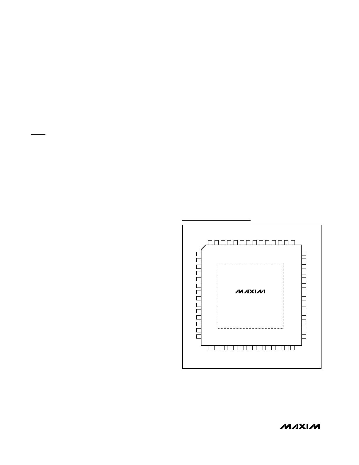
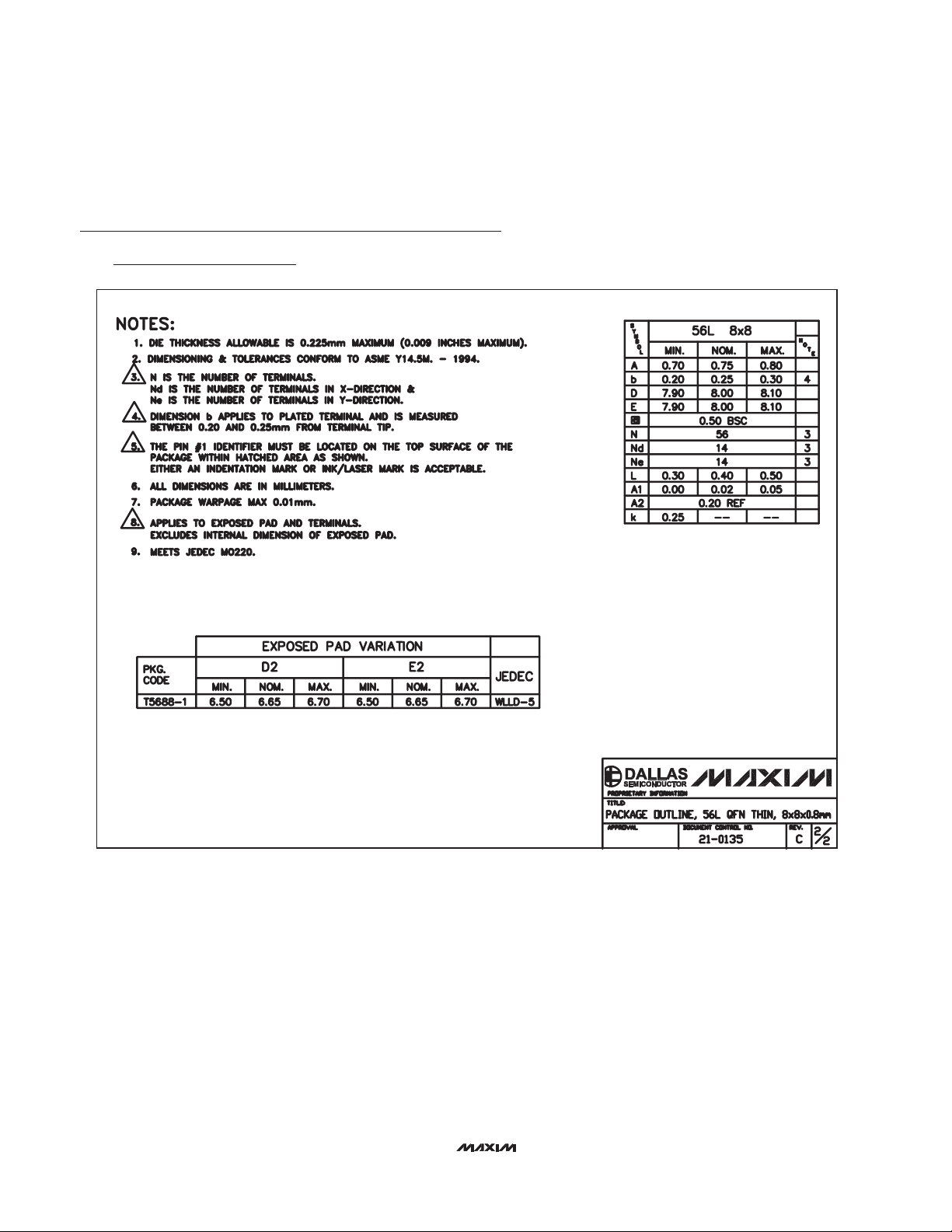
Package Information
(The package drawing(s) in this data sheet may not reflect the most current specifications. For the latest package outline information,
go to www.maxim-ic.com/packages
.)
56L THIN QFN.EPS
Page 18
MAX1427
15-Bit, 80Msps ADC with -79.3dBFS
Noise Floor for Baseband Applications
Maxim cannot assume responsibility for use of any circuitry other than circuitry entirely embodied in a Maxim product. No circuit patent licenses are
implied. Maxim reserves the right to change the circuitry and specifications without notice at any time.
18 ____________________Maxim Integrated Products, 120 San Gabriel Drive, Sunnyvale, CA 94086 408-737-7600
© 2004 Maxim Integrated Products Printed USA is a registered trademark of Maxim Integrated Products.
Package Information (continued)
(The package drawing(s) in this data sheet may not reflect the most current specifications. For the latest package outline information,
go to www.maxim-ic.com/packages
.)
 Loading...