

Page 1
For free samples & the latest literature: http://www.maxim-ic.com, or phone 1-800-998-8800.
For small orders, phone 1-800-835-8769.
General Description
The MAX1425 10-bit, monolithic analog-to-digital converter (ADC) is capable of a 20Msps sampling rate. This
device features an internal track-and-hold (T/H) amplifier
for excellent dynamic performance; at the same time, it
minimizes the number of external components. Low
input capacitance of only 8pF minimizes input drive
requirements. A wide input bandwidth (up to 150MHz)
makes this device suitable for digital RF/IF downconverter applications employing undersampling techniques.
The MAX1425 employs a differential pipelined architecture with a wideband T/H amplifier to maximize throughput while limiting power consumption to only 172mW.
The MAX1425 generates an internal +2.5V reference
that supplies three additional reference voltages
(+3.25V, +2.25V, and +1.25V). These reference voltages provide a differential input range of +2V to -2V.
The analog inputs are biased internally to correct the
DC level, eliminating the need for external biasing on
AC-coupled applications.
A separate +3V digital logic supply input allows for
separation of digital and analog circuitry. The output
data is in two’s complement format. The MAX1425 is
available in the space-saving 28-pin SSOP package.
For a pin-compatible version at a lower data rate, refer
to the MAX1426 data sheet. For a higher data rate, refer
to the MAX1424 data sheet.
Applications
Medical Ultrasound Imaging
CCD Pixel Processing
IR Focal Plane Array
Radar
IF and Baseband Digitization
Set-Top Boxes
Features
♦ Differential Inputs for High Common-Mode
Noise Rejection
♦ Signal-to-Noise Ratio
61dB (at f
IN
= 2MHz)
59.3dB (at f
IN
= 10MHz)
♦ Internal +2.5V Reference
♦ 150MHz Input Bandwidth
♦ Wide ±2V Input Range
♦ Low Power Consumption: 172mW
♦ Separate Digital Supply Input for 3V Logic
Compatibility
♦ Single +5V Supply Operation Possible
MAX1425
10-Bit, 20Msps ADC
________________________________________________________________ Maxim Integrated Products 1
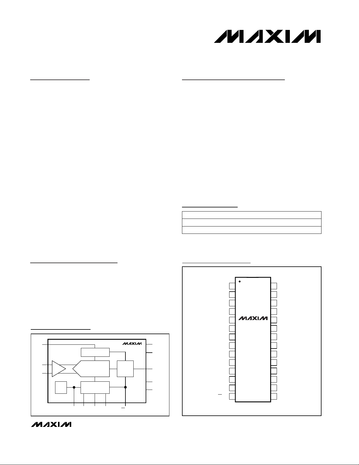
Functional Diagram
19-1597; Rev 0; 1/00
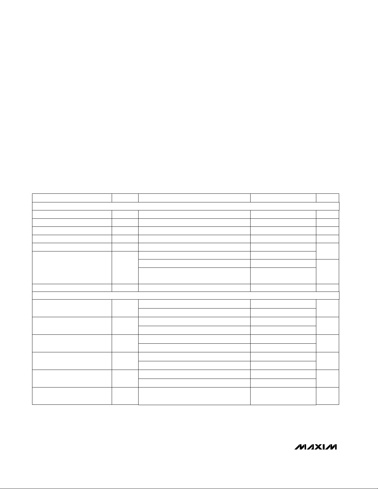
Pin Configuration
Ordering Information
PART
MAX1425CAI
MAX1425EAI -40°C to +85°C
0°C to +70°C
TEMP. RANGE PIN-PACKAGE
28 SSOP
28 SSOP
CLK
INTERFACE
INP
INN
T/H
REF
PIPELINE ADC
REF SYSTEM +
REFIN REFP CML REFN OE/PD
BIAS
AV
MAX1425
OUTPUT
DRIVERS
DD
AGND
D9–D0
DV
DD
DGND
TOP VIEW
AGND
AV
REFP
REFIN
REFN
CML
AGND
AV
INP
INN
CMLP
CMLN
CLK
OE/PD
1
2
DD
3
4
5
MAX1425
6
7
8
DD
9
10
11
12
13
14
SSOP
28
D0
27
D1
26
D2
25
D3
24
D4
23
DGND
22
DV
DD
21
DGND
20
DV
DD
19
D5
18
D6
17
D7
16
D8
15
D9
Page 2
MAX1425
10-Bit, 20Msps ADC
2 _______________________________________________________________________________________
ABSOLUTE MAXIMUM RATINGS
ELECTRICAL CHARACTERISTICS
(V
AV
DD
= V
CMLP
= +5V, V
DV
DD
= +3.3V, V
CMLN
= V
AGND
= V
DGND
= 0, internal reference, digital output load = 35pF, f
CLK
= 20MHz
(50% duty cycle), T
A
= T
MIN
to T
MAX
, unless otherwise noted. Typical values are at TA= +25°C.)
Stresses beyond those listed under “Absolute Maximum Ratings” may cause permanent damage to the device. These are stress ratings only, and functional
operation of the device at these or any other conditions beyond those indicated in the operational sections of the specifications is not implied. Exposure to
absolute maximum rating conditions for extended periods may affect device reliability.
AVDDto AGND ........................................................ -0.3V to +6V
DVDDto DGND ....................................................... -0.3V to +6V
AVDDto DGND........................................................ -0.3V to +6V
DGND to AGND ................................................................. ±0.3V
REFP, REFIN, REFN, CMLN, CMLP,
CML, INP, INN ....................(V
AGND
- 0.3V) to (V
AV
DD
+ 0.3V)
CLK, OE/PD, D0–D9 ...............(V
DGND
- 0.3V) to (V
DV
DD
+ 0.3V)
Continuous Power Dissipation (T
A
= +70°C)
28-Pin SSOP (derated 9.5mW/°C above +70°C) .........762mW
Operating Temperature Ranges
MAX1425CAI ..................................................... 0°C to +70°C
MAX1425EAI................................................... -40°C to +85°C
Junction Temperature..................................................... +150°C
Storage Temperature Range ............................-65°C to +150°C
Lead Temperature (soldering, 10s) .................................+300°C
SINAD
dB
PARAMETER SYMBOL MIN TYP MAX UNITS
Gain Error GE
-10 ±5 10
Midscale Offset MSO
-3 ±1.0 3
No Missing Codes
Integral Nonlinearity INL
-1.5 ±0.3 1.5
LSB
-5 ±2 5
-5 ±3 5
Power-Supply Rejection Ratio PSRR
-5 ±2 5
mV/V
Resolution RES
10
Bits
Differential Nonlinearity DNL
-1 1
LSB
Signal-to-Noise Ratio SNR
60 61
dB
Spurious-Free Dynamic Range SFDR
70 72
dB
Total Harmonic Distortion
(first five harmonics)
THD
-70 -67
dB
Signal-to-Noise and Distortion
59 61
CONDITIONS
f = 2MHz
Internal reference (Note 1)
(Note 1)
Guaranteed monotonic
External reference (REFIN) (Note 2)
External reference (REFP, CML, REFN)
(Note 3)
(Note 4)
f = 2MHz
f = 2MHz
f = 2MHz
%FSR
%FSR
f = 10MHz
56 59
f = 10MHz
64 69
f = 10MHz
-69 -64
f = 10MHz
55 59
ENOB
Bits
Effective Number of Bits
9.3 9.7
f = 2MHz
f = 10MHz
8.8 9.5
IMD
dBc
Intermodulation Distortion
-70
f1 = 10.17MHz, f2 = 10.19MHz
(-7dB FS, each tone) (Note 5)
ACCURACY
DYNAMIC PERFORMANCE (V
INP
- V
INN
= +2V to -2V)
Page 3
MAX1425
10-Bit, 20Msps ADC
_______________________________________________________________________________________ 3
ELECTRICAL CHARACTERISTICS (continued)
(V
AV
DD
= V
CMLP
= +5V, V
DV
DD
= +3.3V, V
CMLN
= V
AGND
= V
DGND
= 0, internal reference, digital output load = 35pF, f
CLK
= 20MHz
(50% duty cycle), T
A
= T
MIN
to T
MAX
, unless otherwise noted. Typical values are at TA= +25°C.)
Common-Mode Reference
Voltage
V
CML
2.25
V(Note 1)
Differential Reference
Temperature Coefficient
±50 ppm/°C
Positive Reference Voltage V
REFP
3.25
V
Common-Mode Reference
Voltage
V
CML
2.25
V
Negative Reference Input
Voltage
V
REFN
1.25
V
Differential Reference
1.9 2.0 2.1
V
Positive Reference V
REFP
3.25
V
V
REFP
- V
REFN,TA
= +25°C
(Note 1)
Input Resistance R
IN
6.5
kΩ
Input Capacitance C
IN
10
pF
Differential Reference
2.0
V
Input Current I
IN
-325 325
µA
Input Capacitance C
IN
15
pF
REFP Input Range
3.25
±10%
V
CML Input Range
2.25
±10%
V
REFN Input Range
1.25
±10%
V
REFIN (Note 8)
REFIN
V
REFP
- V
REFN
REFP, CML, REFN
REFP, CML, REFN
Input Resistance R
IN
3.5
kΩ
Input Capacitance C
IN
8
pF
Input Common-Mode Voltage
Range
V
CMVR
2.25
±10%
V
Differential Input Range DR ±2 V
Small-Signal Bandwidth SSBW 400 MHz
Large-Signal Bandwidth LSBW 150 MHz
Either input to ground
Either input to ground
CML (Note 6)
V
INP
- V
INN
(Note 7)
(Note 7)
PARAMETER SYMBOL MIN TYP MAX UNITSCONDITIONS
Negative Reference V
REFN
1.25
V(Note 1)
Differential Reference
1.8 2 2.2
VV
REFP
- V
REFN
, TA= +25°C
Differential Reference
Temperature Coefficient
±150
ppm/°C
ANALOG INPUT (INP, INN, CML)
REFERENCE (V
REFIN
= 0; REFP, REFN, CML applied externally)
REFERENCE OUTPUTS (REFP, CML, REFN; external +2.5V reference)
REFERENCE OUTPUTS (REFP, CML, REFN; internal +2.5V reference)
Page 4
MAX1425
10-Bit, 20Msps ADC
4 _______________________________________________________________________________________
ELECTRICAL CHARACTERISTICS (continued)
(V
AV
DD
= V
CMLP
= +5V, V
DV
DD
= +3.3V, V
CMLN
= V
AGND
= V
DGND
= 0, internal reference, digital output load = 35pF, f
CLK
= 20MHz
(50% duty cycle), T
A
= T
MIN
to T
MAX
, unless otherwise noted. Typical values are at TA= +25°C.)
I
OE/PD
OE/PD = DV
DD
V
DV
DD
= 5.25V, OE/PD = DV
DD
IOL= 200µA, V
DV
DD
= 2.7V
IOH= -200µA, V
DV
DD
= 2.7V
V
DV
DD
= 5.25V
V
DV
DD
< 4.75V
V
DV
DD
> 4.75V
OE/PD = DV
DD
V
DV
DD
= 5.0V
REFIN = AGND
OE/PD = DV
DD
V
DV
DD
< 4.75V
V
DV
DD
= 3.3V
V
DV
DD
> 4.75V
CONDITIONS
pF10Three-State Capacitance
µA-10 10Three-State Leakage
V0.5VOLOutput Logic Low
V
V
DV
DD
V
DV
DD
- 0.5
VOHOutput Logic High
pF10Input Capacitance
µA-20 20
µA-10 10
Input Current Leakage
0.3 ·
V
DV
DD
V
0.8
V
IL
Input Logic Low
0.7 ·
V
DV
DD
V
2.4
V
IH
Input Logic High
mW
172 220
PDPower Dissipation
µA
90 150
Digital Shutdown Current
8.5 14
mA
26 35
Analog Supply Current with
Internal Reference in Shutdown
nA
0.6 1
Analog Shutdown Current
mA
5.3 9
I
DV
DD
Digital Supply Current
UNITSMIN TYP MAXSYMBOL PARAMETER
Figure 4
Figure 4
ps7t
AJ
Aperture Jitter
ns5t
AD
Aperture Delay
cycles5.5Pipeline Delay (Latency)
ns20 25 30t
CL
Clock Low
ns20 25 30t
CH
Clock High
MHz20f
CLK
Clock Frequency
MHz0.1 20CONVConversion Rate
V
2.7 3.3 5.5
V
DV
DD
Digital Supply Voltage
V
4.75 5.00 5.25
V
AV
DD
Analog Supply Voltage
mA
31 38
I
AV
DD
Analog Supply Current
I
CLK
ns10 20t
AJ
Bus Disable
ns10 20t
AD
Bus Enable
ns52025t
OD
Data Output Delay
POWER SUPPLY
DIGITAL INPUTS (CLK, OE/PD)
DIGITAL OUTPUTS (D0–D9)
TIMING CHARACTERISTICS
Page 5
MAX1425
10-Bit, 20Msps ADC
_______________________________________________________________________________________ 5
ELECTRICAL CHARACTERISTICS (continued)
Note 1: Internal reference, REFIN bypassed to AGND with a 0.1µF capacitor.
Note 2: External +2.5V reference applied to REFIN.
Note 3: Internal reference disabled. V
REFIN
= 0, V
REFP
= 3.25V, V
CML
= 2.25V, and V
REFN
= 1.25V.
Note 4: Measured as the ratio of the change in midscale offset voltage for a ±5% change in V
AV
DD
using the internal reference.
Note 5: IMD is measured with respect to either of the fundamental tones.
Note 6: Specifies the common-mode range of the differential input signal supplied to the MAX1425.
Note 7: Defined as the input frequency at which the fundamental component of the output spectrum is attenuated by 3dB.
Note 8: V
REFIN
is internally biased to +2.5V through a 5kΩ resistor.
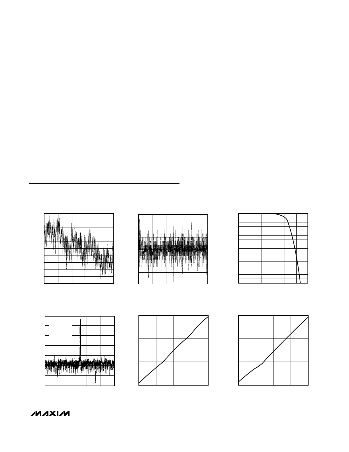
Typical Operating Characteristics
(V
AV
DD
= V
CMLP
= +5V, V
DV
DD
= +3.3V, V
CMLN
= V
AGND
= 0, internal reference, digital output load = 35pF, f
CLK
= 20Msps (50%
duty cycle), for dynamic performance 0dB is full scale, T
A
= +25°C, unless otherwise noted.)
-1.2
-0.6
-0.8
-1.0
-0.4
-0.2
0
0.2
0.4
0.6
0.8
0 400200 600
800
1000
INTEGRAL NONLINEARITY vs. CODE
MAX1425-01
CODE
INL (LSB)
f
INP
= 2MHz
-0.6
-0.2
-0.4
0
0.2
0.4
0.6
0 400200 600
800
1000
DIFFERENTIAL NONLINEARITY vs. CODE
MAX1425-02
CODE
DNL (LSB)
f
INP
= 2MHz
-8.0
-6.0
-7.0
-5.0
-4.0
-3.0
-2.0
-1.0
0
0.01 10.1 10 100 1000 10,000
ANALOG INPUT BANDWIDTH
(FULL POWER)
MAX1425-03
BANDWIDTH (MHz)
AMPLITUDE (dB)
-140
-100
-120
-60
-80
-20
-40
0
042681537910
INTERMODULATION DISTORTION
vs. FREQUENCY
MAX1425-04
FREQUENCY (MHz)
MAGNITUDE (dB)
f
CLK
= 20MHz
f1 = 5.01MHz
f2 = 5.03MHz
f
CLK
= 20MHz
f1 = 5.01MHz
f2 = 5.03MHz
0
20
40
60
SIGNAL-TO-NOISE PLUS DISTORTION
vs. POWER (f
IN
= 2.003MHz)
MAX1425-05
INPUT (dB)
SINAD (dB)
-60 -30-45 -15 0
0
20
40
60
SIGNAL-TO-NOISE RATIO PLUS DISTORTION
vs. POWER (f
IN
= 5.009MHz)
MAX1425-06
INPUT (dB)
SNDR (dB)
-60 -30-45 -15 0
Page 6
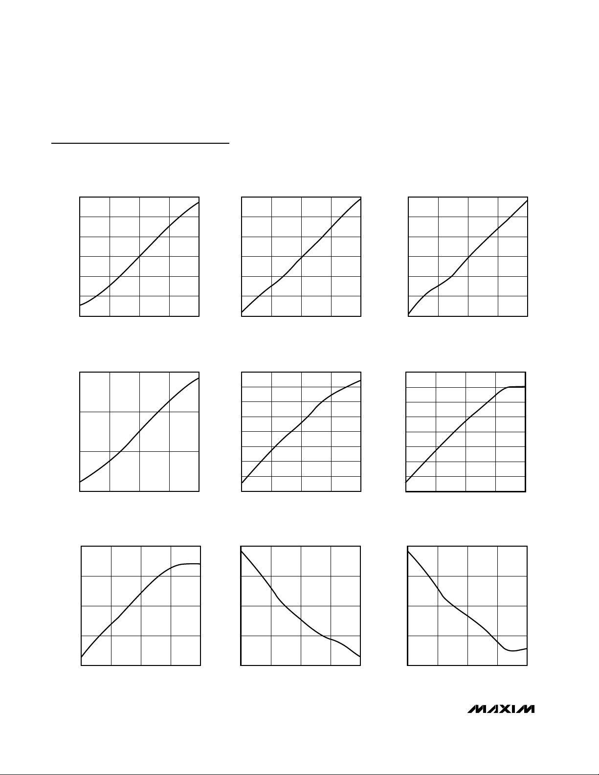
0
20
40
60
80
SPURIOUS-FREE DYNAMIC RANGE
vs. POWER (f
IN
= 9.984MHz)
MAX1425-13
INPUT (dB)
SFDR (dB)
-60 -30-45 -15 0
-80
-60
-40
-20
0
TOTAL HARMONIC DISTORTION
vs. POWER (f
IN
= 2.003MHz)
MAX1425-14
INPUT (dB)
THD (dB)
-60 -30-45 -15 0
-80
-60
-40
-20
0
TOTAL HARMONIC DISTORTION
vs. POWER (f
IN
= 5.009MHz)
MAX1425-15
INPUT (dB)
THD (dB)
-60 -30-45 -15 0
MAX1425
10-Bit, 20Msps ADC
6 _______________________________________________________________________________________
Typical Operating Characteristics (continued)
(V
AV
DD
= V
CMLP
= +5V, V
DV
DD
= +3.3V, V
CMLN
= V
AGND
= 0, internal reference, digital output load = 35pF, f
CLK
= 20Msps (50%
duty cycle), for dynamic performance 0dB is full scale, T
A
= +25°C, unless otherwise noted.)
0
20
10
30
40
50
60
SIGNAL-TO-NOISE PLUS DISTORTION
vs. POWER (f
IN
= 9.884MHz)
MAX1425-07
INPUT (dB)
SINAD (dB)
-60 -30-45 -15 0
0
20
40
60
SIGNAL-TO-NOISE RATIO
vs. POWER (f
IN
= 9.884MHz)
MAX1425-10
INPUT (dB)
SNR (dB)
-60 -30-45 -15 0
0
20
10
30
40
50
60
SIGNAL-TO-NOISE RATIO
vs. POWER (f
IN
= 2.003MHz)
MAX1425-08
INPUT (dB)
SNR (dB)
-60 -30-45 -15 0
0
20
10
30
40
50
60
SIGNAL-TO-NOISE RATIO
vs. POWER (f
IN
= 5.009MHz)
MAX1425-09
INPUT (dB)
SNR (dB)
-60 -30-45 -15 0
0
20
10
30
40
50
60
70
80
SPURIOUS-FREE DYNAMIC RANGE
vs. POWER (f
IN
= 2.003MHz)
MAX1425-11
INPUT (dB)
SFDR (dB)
-60 -30-45 -15 0
0
20
10
30
40
50
60
70
80
SPURIOUS-FREE DYNAMIC RANGE
vs. POWER (f
IN
= 5.009MHz)
MAX1425-12
INPUT (dB)
SFDR (dB)
-60 -30-45 -15 0
Page 7
MAX1425
10-Bit, 20Msps ADC
_______________________________________________________________________________________ 7
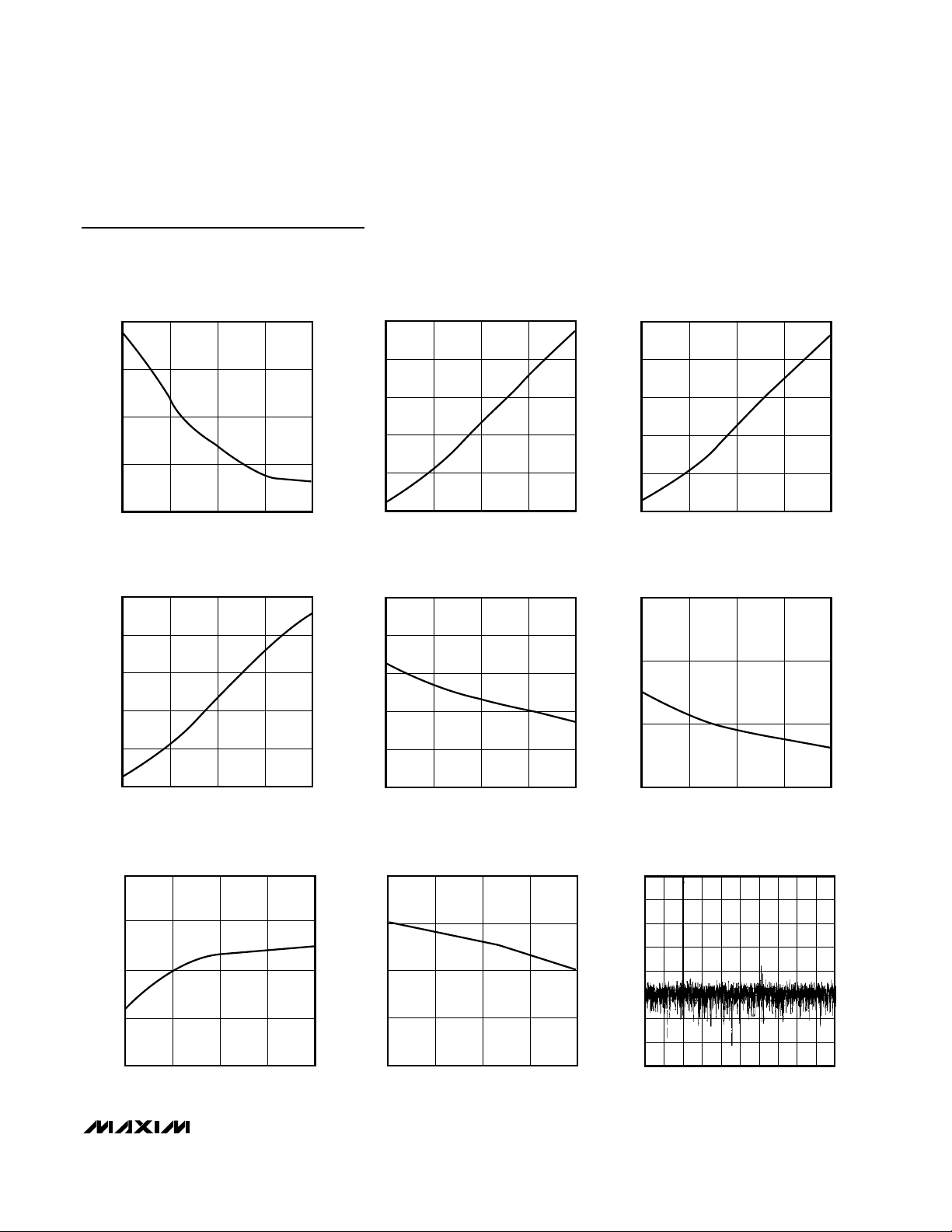
Typical Operating Characteristics (continued)
(V
AV
DD
= V
CMLP
= +5V, V
DV
DD
= +3.3V, V
CMLN
= V
AGND
= 0, internal reference, digital output load = 35pF, f
CLK
= 20Msps (50%
duty cycle), for dynamic performance 0dB is full scale, T
A
= +25°C, unless otherwise noted.)
-80
-70
-60
TOTAL HARMONIC DISTORTION
vs. INPUT FREQUENCY
MAX1425-22
INPUT FREQUENCY (MHz)
THD (dB)
264810
-65
-75
57
59
58
60
61
SIGNAL-TO-NOISE PLUS DISTORTION
vs. INPUT FREQUENCY
MAX1425-23
INPUT FREQUENCY (MHz)
SINAD (dB)
264810
-160
-120
-140
-100
-40
-20
-60
-80
0
0 23451 678910
FFT PLOT (fIN = 2MHz)
MAX1425-24
FREQUENCY (MHz)
MAGNITUDE (dB)
0
-20
-40
THD (dB)
-60
-80
-60 -30-45 -15
10
8
6
TOTAL HARMONIC DISTORTION
vs. POWER (f
= 9.884MHz)
IN
INPUT (dB)
EFFECTIVE NUMBER OF BITS
vs. POWER (f
= 9.884MHz)
IN
0
MAX1425-16
MAX1425-19
10
8
6
ENOB (bits)
4
2
0
-60 -30-45 -15 0
10.0
9.6
9.2
EFFECTIVE NUMBER OF BITS
vs. POWER (f
= 2.003MHz)
IN
INPUT (dB)
MAX1425-17
ENOB (bits)
EFFECTIVE NUMBER OF BITS
vs. POWER (f
10
8
6
4
2
0
-60 -30-45 -15 0
EFFECTIVE NUMBER OF BITS
vs. INPUT FREQUENCY
60
MAX1425-20
59
= 5.009MHz)
IN
INPUT (dB)
SIGNAL-TO-NOISE RATIO
vs. INPUT FREQUENCY
MAX1425-18
MAX1425-21
ENOB (bits)
4
2
0
-60 -30-45 -15 0
INPUT (dB)
ENOB (bits)
8.8
8.4
8.0
264810
INPUT FREQUENCY (MHz)
SNR (dB)
58
57
264810
INPUT FREQUENCY (MHz)
Page 8

MAX1425
10-Bit, 20Msps ADC
8 _______________________________________________________________________________________
Typical Operating Characteristics (continued)
(V
AV
DD
= V
CMLP
= +5V, V
DV
DD
= +3.3V, V
CMLN
= V
AGND
= 0, internal reference, digital output load = 35pF, f
CLK
= 20Msps (50%
duty cycle), for dynamic performance 0dB is full scale, T
A
= +25°C, unless otherwise noted.)
-140
-100
-120
-60
-80
-20
-40
0
042681537910
FFT PLOT (fIN = 5MHz)
MAX1425-25
FREQUENCY (MHz)
MAGNITUDE (dB)
28
32
40
36
44
48
0.50
0.55
0.65
0.60
0.70
0.75
-40 -15 10 35 60 85
TOTAL SUPPLY CURRENT
vs. TEMPERATURE
MAX1425-27
TEMPERATURE (°C)
SUPPLY CURRENT (mA)
SHUTDOWN CURRENT (mA)
SHUTDOWN
REFIN = AGND
OE/PD = 1
-140
-100
-120
-60
-80
-20
-40
0
042681537910
FFT PLOT (fIN = 10MHz)
MAX1425-26
FREQUENCY (MHz)
MAGNITUDE (dB)
2.08
2.10
2.14
2.12
2.16
2.18
-40 -15 10 35 60 85
INTERNAL REFERENCE VOLTAGE
vs. TEMPERATURE
MAX1425-28
TEMPERATURE (°C)
INTERNAL REFERENCE (V)
Page 9

MAX1425
10-Bit, 20Msps ADC
_______________________________________________________________________________________ 9
Pin Description
Common-Mode Level Positive Input. For AC applications, connect to AVDDto internally set the input
DC bias level. For DC-coupled applications, connect to AGND.
CMLP11
Common-Mode Level Negative Input. Connect to AGND to internally set the input DC bias level for
both AC- and DC-coupled applications.
CMLN12
Clock Input. Clock frequency range from 0.1MHz to 20MHz.CLK13
Active-Low Output Enable and Power-Down Input. Digital outputs become high impedance and
device enters low-power mode when pin is high.
OE/PD
14
Digital Data Output (MSB)D915
Negative Reference Output. Bypass to AGND with a 0.1µF capacitor. REFN can accept an external
voltage when the internal reference is disabled (REFN = AGND).
REFN5
Common-Mode Level Input. Bypass to AGND with a 0.1µF capacitor. CML can accept an external
voltage when the internal reference is disabled (REFN = AGND).
CML6
Positive Analog Signal InputINP9
Negative Analog Signal InputINN10
External Reference Input. Bypass to AGND with a 0.1µF capacitor. REFIN can be biased externally
to adjust the reference level and calibrate full-scale errors. To disable the internal reference, connect
REFIN to AGND.
REFIN4
Positive Reference Output. Bypass to AGND with a 0.1µF capacitor. If the internal reference is
disabled, REFP can accept an external voltage.
REFP3
PIN
Analog Supply Voltage Input. Bypass with a parallel combination of 2.2µF, 0.1µF, and 100pF capacitors
to AGND. Bypass each supply input to the closest AGND (e.g., capacitors between pins 1 and 2).
AV
DD
2, 8
Analog Ground. Connect all return paths for analog signals to these pins.AGND1, 7
FUNCTIONNAME
Digital Data Outputs 4–1D4–D124–27
Digital Data Output (LSB)D028
Digital Supply Voltage Input. Bypass with 2.2µF and 0.1µF capacitors in parallel. Digital supply can
operate with voltages as low as +2.7V.
DV
DD
20, 22
Digital GroundDGND21, 23
Digital Data Outputs 8–5D8–D516–19
Page 10

MAX1425
10-Bit, 20Msps ADC
10 ______________________________________________________________________________________
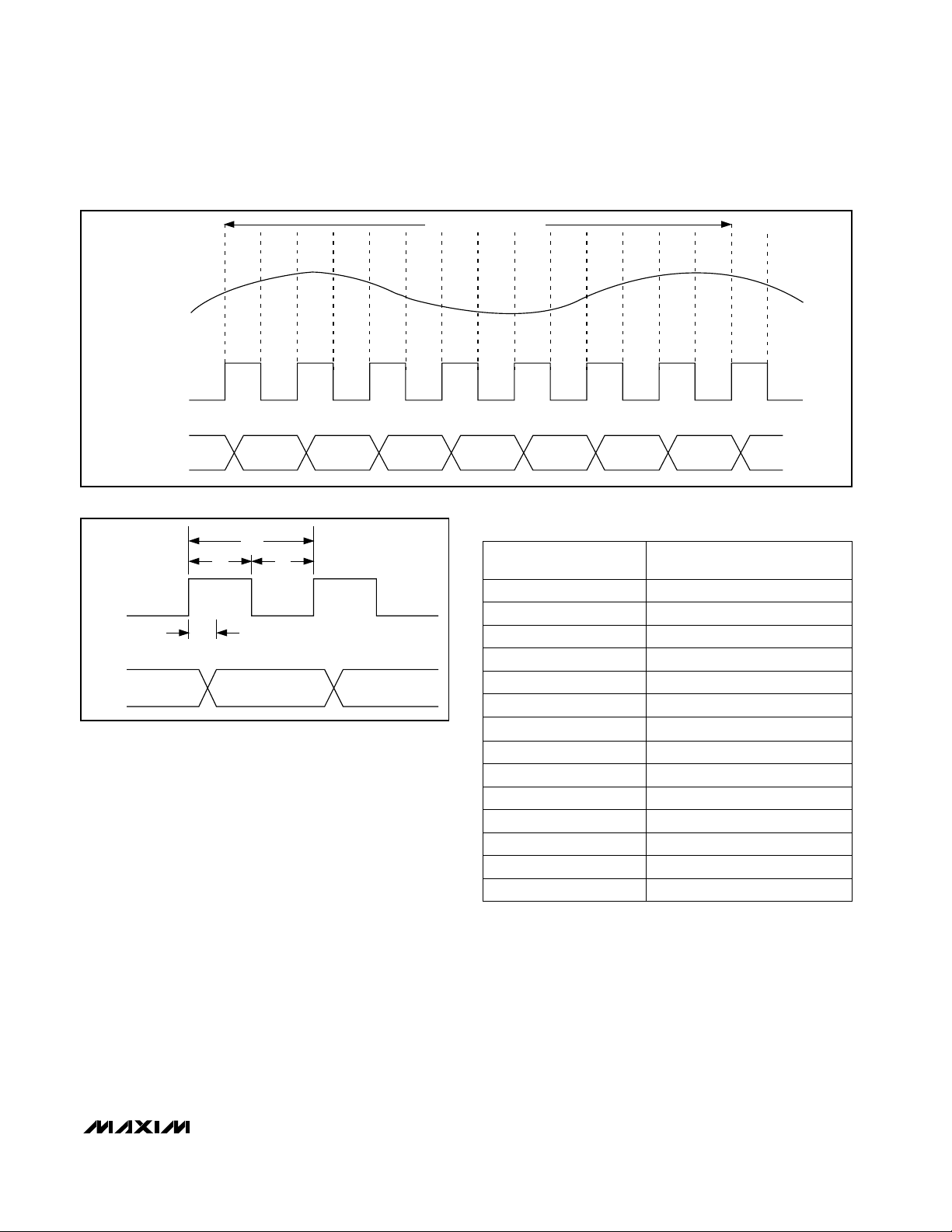
Detailed Description
The MAX1425 uses a 10-stage, fully differential, pipelined
architecture (Figure 1) that allows for high-speed conversion while minimizing power consumption. Each sample
moves through a pipeline stage every half clock cycle.
Counting the delay through the output latch, there is a 5.5
clock-cycle latency.
A 2-bit flash ADC converts the input voltage to digital
code. A DAC converts the ADC result back into an analog voltage, which is subtracted from the held input signal. The resulting error signal is then multiplied by two,
and this product is passed along to the next pipeline
stage where the process is repeated. Digital error correction compensates for offsets and mismatches in each
pipeline stage and ensures no missing codes.
Internal Track-and-Hold Circuit
Figure 2 shows a simplified functional diagram of the
internal track-and-hold (T/H) circuit in both track mode
and hold mode. The fully differential circuit samples the
input signal onto the four capacitors C1a, C1b, C2a,
and C2b. Switches S2a and S2b set the common mode
for the amplifier input, and open before S1. When S1
opens, the input is sampled. Switches S3a and S3b
then connect capacitors C1a and C1b to the output of
the amplifier. Capacitors C2a and C2b are connected
either to REFN, REFP, or each other, depending on the
results of the flash ADC. The amplifier then multiplies
the residue by two and the next stage in the pipeline
performs a similar operation.
System Timing Requirements
Figure 3 shows the relationship between the clock
input, analog input, and data output. The MAX1425
samples the falling edge of the input clock. Output data
is valid on the rising edge of the input clock. The output
data has an internal latency of 5.5 clock cycles, as
shown. Figure 4 shows an output timing diagram that
specifies the relationship between the input clock parameters and the valid output data.
Analog Input and Internal Reference
The MAX1425 has an internal +2.5V reference used to
generate three reference levels: +3.25V, +2.25V, and
+1.25V corresponding to V
REFP
, V
CML
, and V
REFN
.
These reference voltages enable a ±2V input range.
Bypass all reference voltages with a 0.1µF capacitor.
The MAX1425 allows for three modes of reference
operation: an internal reference (default) mode, an
externally adjusted reference mode, or a full external
reference mode. The internal reference mode occurs
when no voltages are applied to REFIN, REFP, CML,
Figure 1. Pipelined A/D Architecture (Block)
Figure 2. Internal Track-and-Hold Circuit
MDAC
V
IN
V
IN
T/H
FLASH
ADC
2 BITS
STAGE 1 STAGE 2
Σ
DAC
DIGITAL CORRECTION LOGIC
10
D [9:0]
V
OUT
x2
STAGE 10
CML
S4c
S4c
C1a
C2a
C2b
C1b
C1a
C2a
C2b
C1b
S2a
S1
S2b
CML
CML
S2a
S1
S2b
CML
INP
REFP
REFN
REFP
REFN
INN
a) TRACK MODE
INP
REFP
REFN
REFP
REFN
INN
b) HOLD MODE
S3a
S4a
S4b
S3a
S4a
S4b
S3b
Page 11
MAX1425
10-Bit, 20Msps ADC
______________________________________________________________________________________ 11
and REFN. In this mode, the voltages at these pins
are set to their nominal values (see Electrical
Characteristics). The reference voltage levels can be
adjusted externally by applying a voltage at REFIN.
This allows other input levels to be used as well. The
full external reference mode is entered when REFIN =
AGND. External voltages can be applied to REFP,
CML, and REFN. In this mode, the internal reference
shuts down, resulting in less overall power consumption.
Clock Input (CLK)
CLK is TTL/CMOS-compatible. Since the interstage
conversion of the device depends on the rising and
falling edges of the external clock, use a clock with low
jitter and fast rise and fall times (<2ns). Low clock jitter
improves SNR performance. The MAX1425 operates
with a 50% duty cycle. If the clock has a duty cycle
other than 50%, the clock must meet the specifications
for high and low periods as stated in the Electrical
Characteristics.
Output Enable/Power-Down Function
(
OE
/PD) and Output Data
All data outputs, D0 through D9, are TTL/CMOS-logic
compatible. There is a 5.5 clock-cycle latency between
the start convert signal and the valid output data. The
output coding for the MAX1425 is in binary two’s complement format, which has the MSB inverted (Table 1).
The digital output goes into a high-impedance state
and the device into a low-power mode when OE/PD
goes high. For normal operation, drive OE low. The outputs are not designed to drive high capacitances or
Figure 3. System Timing Diagram
Figure 4. Output Timing Diagram
1 1 1 1 1 1 1 1 1 1 -1 LSB
1 1 1 0 0 0 0 0 0 0-1/4 Full Scale
1 1 0 0 0 0 0 0 0 0-1/2 Full Scale
0 1 0 0 0 0 0 0 0 0+1/2 Full Scale
0 0 1 0 0 0 0 0 0 0+1/4 Full Scale
0 0 0 0 0 0 0 0 0 1+1 LSB
0 0 0 0 0 0 0 0 0 0Bipolar Zero
0 1 1 0 0 0 0 0 0 0+3/4 Full Scale
0 1 1 1 1 1 1 1 0 1+Full Scale 2LSB
0 1 1 1 1 1 1 1 1 0 +Full Scale 1LSB
0 1 1 1 1 1 1 1 1 1 +Full Scale
OUTPUT CODE
(TWO’S COMPLEMENT)
DIFFERENTIAL INPUT
Table 1. MAX1425 Output Code
1 0 1 0 0 0 0 0 0 0-3/4 Full Scale
1 0 0 0 0 0 0 0 0 1-Full Scale + 1LSB
1 0 0 0 0 0 0 0 0 0-Full Scale
5.5 CLOCK-CYCLE LATENCY
ANALOG INPUT
CLOCK INPUT
DATA OUTPUT
INPUT
CLK
t
OD
OUTPUT
DATA
DATA 0
n - 6
t
CLK
t
CH
DATA 1 DATA 2
n
t
CI
n - 5
n + 1
n + 2
n - 4
n + 3
n - 3
n - 2
n + 4
n - 1
n + 5
n + 6
n
n + 7
n + 1
Page 12

MAX1425
10-Bit, 20Msps ADC
12 ______________________________________________________________________________________
Figure 5. Typical Application Circuit Using the Internal Reference
heavy loads, as they are specified to deliver only
200µA for TTL compatibility. If an application needs
output buffering, use 74LS74s or 74ALS541s as
required.
Applications Information
Figure 5 depicts a typical application circuit containing
a single-ended to differential converter. The internal reference provides a +2.25V output for level shifting. The
input is buffered and then split to a voltage follower and
inverter. The op amps are followed by a lowpass filter
to remove some of the wideband noise associated with
high-speed op amps. In this application, the amplifier
outputs are directly coupled to the inputs. This configuration can also be modified for AC-coupled applications.
The MAX1425 includes a DC level-shifting circuit internal
to the part, allowing for AC-coupled applications. The
level-shifting circuit is shown in Figure 6.
The circuit in Figure 6 can accept a 1Vp-p maximum
input voltage. With a maximum clock frequency of
20MHz, use 50Ω termination to minimize reflections.
Buffer the digital outputs with a low-cost, high-speed,
300Ω
300Ω
0.1µF
600Ω
+5V
MAX4108
-5V
2.5k
MAX473A
0.1µF
BAS16
0.1µF
0.1µF
600Ω
+5V
0.1µF
300Ω
50Ω
INP
22pF
CML
MAX1425
0.1µF
INPUT
50Ω
MAX4108
25Ω
+5V
-5V
25Ω
0.1µF
0.1µF
0.1µF
600Ω
300Ω
300Ω
2.5k
+5V
MAX4108
-5V
0.1µF
0.1µF
600Ω
50Ω
300Ω
0.1µF
BAS16
50Ω
22pF
INN
Page 13

MAX1425
10-Bit, 20Msps ADC
______________________________________________________________________________________ 13
octal D-latched flip-flop (74ALS374), or use octal
buffers such as the 74ALS541.
Typical Application Using an
External Reference
Figure 7 depicts an application circuit that shuts down
the internal reference, allowing an external reference to
be used for selecting a different common-mode voltage. This added flexibility also allows for ratiometric
conversions, as well as for calibration.
Using Transformer Coupling
A small transformer (Figure 8) provides isolation and
AC-coupling to the ADC’s input. Connecting the transformer’s center tap to CML provides a +2.25VDC level
shift to the input. Transformer coupling reduces the
need for high-speed op amps, thereby reducing cost.
Although a 1:1 transformer is shown, a step-up transformer may be selected to reduce the drive requirements.
Single-Ended DC-Coupled Input Signal
Figure 9 shows an AC-coupled, single-ended application. The MAX4108 quad op amp provides high speed,
high bandwidth, low noise, and low distortion to maintain the integrity of the input signal.
Figure 6. Analog Input DC Bias Circuit
Figure 7. Using an External Reference for REFP, REFN, and CML (internal reference shut down)
CMLP
5.5k 5.5k
INP
V
DD
2
R
V
DD
4
R
TO T/H INPUT
MAX4284
MAX4284
INN
4.5k
CMLN
V
DD
R
R
4.5k
50Ω
0.1µF
50Ω
R
V
DD
2
R
50Ω
R
V
DD
4
0.1µF
0.1µF
CML
REFP
REFN
REFIN
V
DD
( )
2
V
DD
+ 1V
( )
2
MAX1425
V
DD
- 1V
( )
2
AGND
R
+1V
Page 14

MAX1425
10-Bit, 20Msps ADC
14 ______________________________________________________________________________________
Bypassing and Board Layout
The MAX1425 requires high-speed board layout design
techniques. Locate all bypass capacitors as close to
the device as possible, using surface-mount devices
for minimum inductance. Bypass all analog voltages
(AV
DD
, REFIN, REFP, REFN, and CML) to AGND.
Bypass the digital supply (DVDD) to DGND. Multilayer
boards with separated ground and power planes produce the highest level of signal integrity. Route highspeed digital signal traces away from sensitive analog
traces. Matching impedance, especially for the input
clock generator, may reduce reflections, thus providing
less jitter in the system. For optimum results, use lowdistortion complementary components such as the
MAX4108.
Figure 8. Using a Transformer for AC-Coupling
Figure 9. Single-Ended AC-Coupled Input Signal
TRANSISTOR COUNT: 5305
Chip Information
R4
25Ω
C3
IN1
N.C.
R2
100Ω
R3
100Ω
1
T1
2
MINICIRCUITS
KKB1
22pF
6
5
0.1µF
43
R5
25Ω
C9
22pF
MAX1425
CML
INP
V
IN
±V
MAX4108
50Ω
±2V
0.1µF
100Ω
100Ω
50Ω
22pF
0.1µF
INP
MAX1425
INN
Page 15
MAX1425
10-Bit, 20Msps ADC
______________________________________________________________________________________ 15
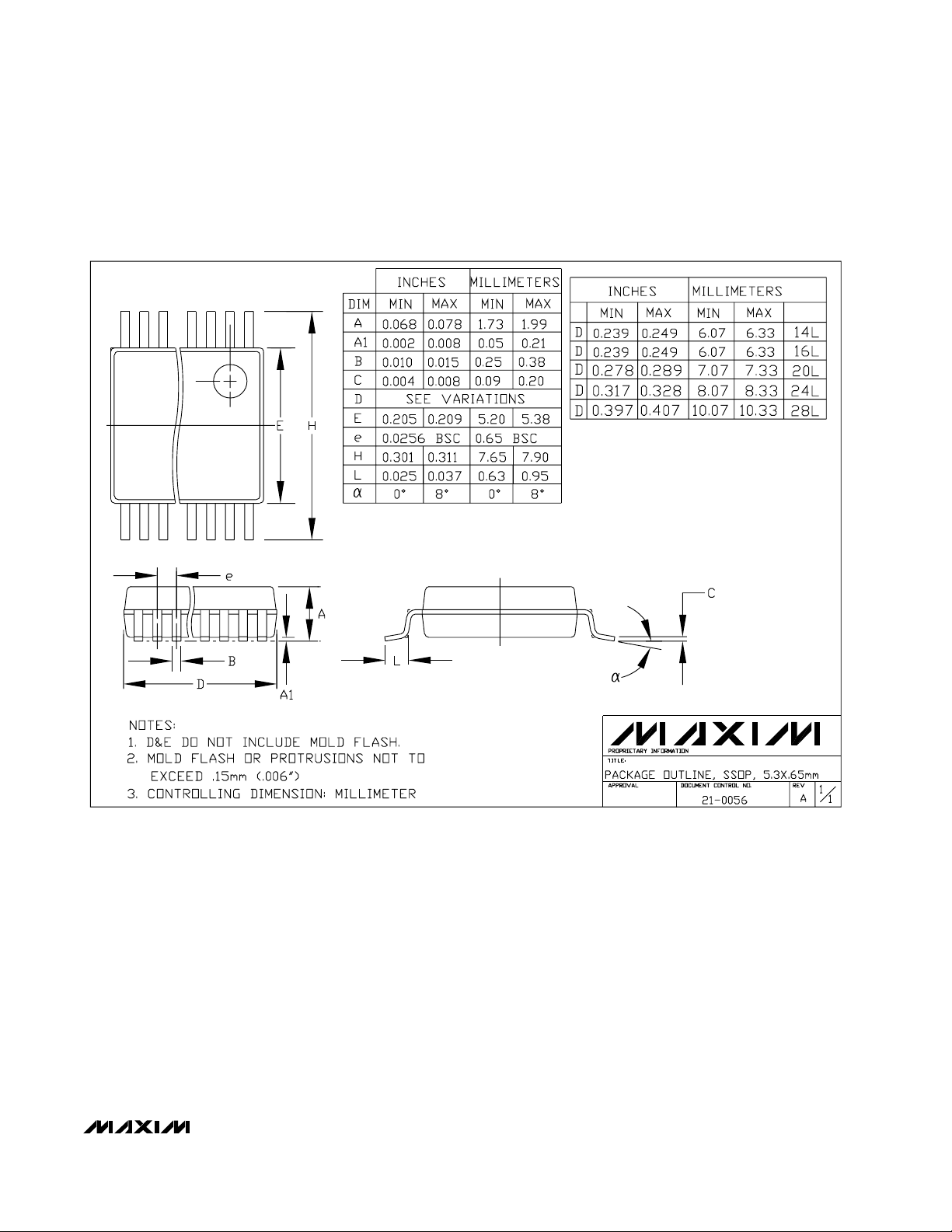
________________________________________________________Package Information
SSOP.EPS
Page 16

MAX1425
10-Bit, 20Msps ADC
Maxim cannot assume responsibility for use of any circuitry other than circuitry entirely embodied in a Maxim product. No circuit patent licenses are
implied. Maxim reserves the right to change the circuitry and specifications without notice at any time.
16 ____________________Maxim Integrated Products, 120 San Gabriel Drive, Sunnyvale, CA 94086 408-737-7600
© 2000 Maxim Integrated Products Printed USA is a registered trademark of Maxim Integrated Products.
NOTES
 Loading...