

Page 1
For free samples & the latest literature: http://www.maxim-ic.com, or phone 1-800-998-8800.
For small orders, phone 1-800-835-8769.
General Description
The MAX1402 low-power, multichannel, serial-output
analog-to-digital converter (ADC) features matched
200µA current sources for sensor excitation. This ADC
uses a sigma-delta modulator with a digital decimation
filter to achieve 16-bit accuracy. The digital filter’s userselectable decimation factor allows the conversion resolution to be reduced in exchange for a higher output
data rate. True 16-bit performance is achieved at an
output data rate of up to 480sps. In addition, the modulator sampling frequency may be optimized for either
lowest power dissipation or highest throughput rate.
The MAX1402 operates from a +5V supply.
This device offers three fully differential input channels
that may be independently programmed with a gain
between +1V/V and +128V/V. Furthermore, it can compensate an input-referred DC offset up to 117% of the
selected full-scale range. These three differential channels may also be configured to operate as five pseudodifferential input channels. Two additional, fully
differential system-calibration channels are provided for
gain and offset error correction.
The MAX1402 may be configured to sequentially scan all
signal inputs and provide the results via the serial interface with minimum communications overhead. When
used with a 2.4576MHz or 1.024MHz master clock, the
digital decimation filter can be programmed to produce
zeros in its frequency response at the line frequency and
associated harmonics, ensuring excellent line rejection
without the need for further post-filtering.
The MAX1402 is available in a 28-pin SSOP package.
Applications
Portable Industrial Instruments
Portable Weigh Scales
Loop-Powered Systems
Pressure Transducers
Features
♦ 18-Bit Resolution, Sigma-Delta ADC
♦ 16-Bit Accuracy with No Missing Codes to 480sps
♦ Low Quiescent Current
250µA (operating mode)
2µA (power-down mode)
♦ Matched On-Board Current Sources (200µA) for
Sensor Excitation
♦ 3 Fully Differential or 5 Pseudo-Differential Signal
Input Channels
♦ 2 Additional, Fully Differential Calibration
Channels/Auxiliary Input Channels
♦ Programmable Gain and Offset
♦ Fully Differential Reference Inputs
♦ Converts Continuously or On Command
♦ Automatic Channel Scanning and Continuous
Data Output Mode
♦ Operates with +5V Analog Supply and +3V or +5V
Digital Supply
♦ 3-Wire Serial Interface—SPI™/QSPI™ Compatible
♦ 28-Pin SSOP Package
MAX1402
+5V, 18-Bit, Low-Power, Multichannel,
Oversampling (Sigma-Delta) ADC
________________________________________________________________
Maxim Integrated Products
1
28
27
26
25
24
23
22
21
20
19
18
17
16
15
1
2
3
4
5
6
7
8
9
10
11
12
13
14
SCLK
DIN
DOUT
INT
V
DD
DGND
AIN5
CALOFF+
CALOFFREFIN+
REFINCALGAIN+
CALGAINAIN6
AIN4
AIN3
AIN2
AIN1
V+
AGND
OUT1
OUT2
DS0
DS1
RESET
CS
CLKOUT
CLKIN
SSOP
TOP VIEW
MAX1402
PART
MAX1402CAI
MAX1402EAI -40°C to +85°C
0°C to +70°C
TEMP. RANGE PIN-PACKAGE
28 SSOP
28 SSOP
Pin Configuration
Ordering Information
EVALUATION KIT
AVAILABLE
SPI and QSPI are trademarks of Motorola, Inc.
19-1423; Rev 0; 3/99
Page 2
%FSR
MAX1402
+5V, 18-Bit, Low-Power, Multichannel,
Oversampling (Sigma-Delta) ADC
2 _______________________________________________________________________________________
ABSOLUTE MAXIMUM RATINGS
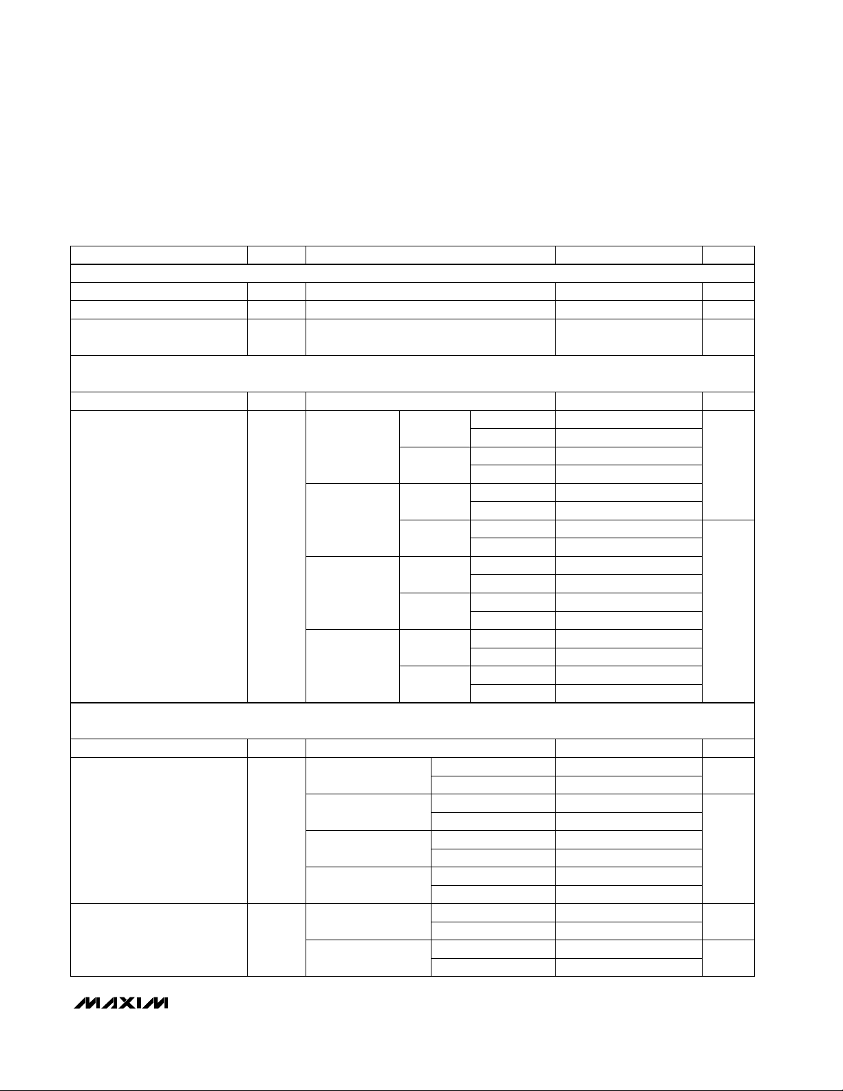
ELECTRICAL CHARACTERISTICS
(V+ = +5V ±5%, VDD= +2.7V to +5.25V, V
REFIN+
= +2.50V, REFIN- = AGND, f
CLKIN
= 2.4576MHz, TA= T
MIN
to T
MAX
, unless other-
wise noted. Typical values are at T
A
= +25°C.)
Stresses beyond those listed under “Absolute Maximum Ratings” may cause permanent damage to the device. These are stress ratings only, and functional
operation of the device at these or any other conditions beyond those indicated in the operational sections of the specifications is not implied. Exposure to
absolute maximum rating conditions for extended periods may affect device reliability.
V+ to AGND, DGND.................................................-0.3V to +6V
V
DD
to AGND, DGND...............................................-0.3V to +6V
AGND to DGND.....................................................-0.3V to +0.3V
Analog Inputs to AGND................................-0.3V to (V+ + 0.3V)
Analog Outputs to AGND.............................-0.3V to (V+ + 0.3V)
Reference Inputs to AGND...........................-0.3V to (V+ + 0.3V)
CLKIN and CLKOUT to DGND...................-0.3V to (V
DD
+ 0.3V)
All Other Digital Inputs to DGND..............................-0.3V to +6V
All Digital Outputs to DGND.......................-0.3V to (V
DD
+ 0.3V)
Maximum Current Input into Any Pin ..................................50mA
Continuous Power Dissipation (TA= +70°C)
28-Pin SSOP (derate 9.52mW/°C above +70°C) ........524mW
Operating Temperature Ranges
MAX1402CAI .....................................................0°C to +70°C
MAX1402EAI...................................................-40°C to +85°C
Storage Temperature Range.............................-60°C to +150°C
Lead Temperature (soldering, 10sec).............................+300°C
µV/°C
For gains of 1, 2, 4
No missing codes guaranteed by design;
for filter settings with FS1 = 0
For gains of 1, 2, 4, 8, 16, 32, 64
For gain of 128
For gains of 1, 2, 4, 8, 16, 32, 64
For gain of 128
For gains of 1, 2, 4, 8, 16, 32, 64
For gain of 128
For gains of 1, 2, 4
For gains of 1, 2, 4, 8, 16, 32, 64
For gains of 8, 16, 32, 64, 128
For gains of 1, 2, 4
Depends on filter setting and selected gain
Bipolar mode, filter settings with FS1 = 0
Relative to nominal of 1% FSR
For gains of 8, 16, 32, 64, 128
CONDITIONS
0.8
%FSR
-2.5 2.5
Bipolar Negative Full-Scale Error
ppm/°C
5
Gain-Error Drift (Note 5)
1
%FSR
-3 3
Gain Error (Note 4)
-2 2
%FSR
-3.5 3.5
-2.5 2.5
Positive Full-Scale Error
(Note 2)
0.3
Bipolar Zero Drift
Bits16Noise-Free Resolution
0.8
%FSR-2.0 2.0Bipolar Zero Error
µV/°C
0.3
Unipolar Offset Drift
0.5
Table 16Output Noise
%FSR-0.0015 0.0015INLIntegral Nonlinearity
0.98Nominal Gain (Note 1)
%FSR-1 2Unipolar Offset Error
UNITSMIN TYP MAXSYMBOLPARAMETER
For gains of 8, 16, 32, 64, 128
µV/°C
0.3
Bipolar Negative Full-Scale Drift
For gains of 8, 16, 32, 64, 128
For gains of 1, 2, 4
µV/°C
0.3
0.8
Full-Scale Drift (Note 3)
For gain of 128 -3.5 3.5
STATIC PERFORMANCE
Page 3
MAX1402
+5V, 18-Bit, Low-Power, Multichannel,
Oversampling (Sigma-Delta) ADC
_______________________________________________________________________________________ 3
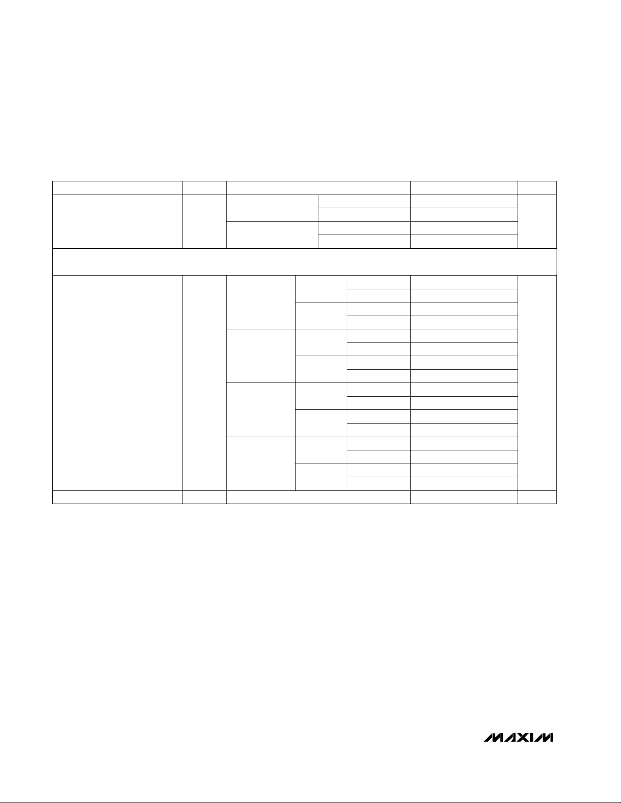
ELECTRICAL CHARACTERISTICS (continued)
(V+ = +5V ±5%, VDD= +2.7V to +5.25V, V
REFIN+
= +2.50V, REFIN- = AGND, f
CLKIN
= 2.4576MHz, TA= T
MIN
to T
MAX
, unless other-
wise noted. Typical values are at T
A
= +25°C.)
BUFF = 0
BUFF = 1
Bipolar mode
REFIN and AIN for
BUFF = 0
BUFF = 1
Unipolar mode
REFIN and AIN for BUFF = 0
REFIN and AIN for BUFF = 0
For filter notch 60Hz, ±0.02 · f
NOTCH
,
MF1 = 0, MF0 = 0, f
CLKIN
= 2.4576MHz
For filter notch 50Hz, ±0.02 · f
NOTCH
,
MF1 = 0, MF0 = 0, f
CLKIN
= 2.4576MHz
At DC
For filter notch 60Hz, ±0.02 · f
NOTCH
,
MF1 = 0, MF0 = 0, f
CLKIN
= 2.4576MHz (Note 8)
DAC code = 0000
Unipolar mode
Bipolar mode
Input Referred
For filter notch 50Hz, ±0.02 · f
NOTCH
,
MF1 = 0, MF0 = 0, f
CLKIN
= 2.4576MHz (Note 8)
CONDITIONS
pF
34
AIN Input Capacitance
(Notes 11)
nA10AIN Input Current (Note 10)
nA10
pA40
DC Input Leakage Current
(Note 10)
V
V
AGND
V+
+ 200mV - 1.5
Absolute and Common-Mode
AIN Voltage Range
V
V
AGND
V+
- 30mV + 30mV
Absolute Input Voltage Range
dBV
AGND
V+
Common-Mode Voltage Range
(Note 9)
dB100NMR
Normal Mode 60Hz Rejection
(Note 8)
dB100NMR
Normal Mode 50Hz Rejection
(Note 8)
150
150
-58.35 58.35
%FSR
-116.7 116.7
Offset DAC Range (Note 6)
dB
90
CMRCommon-Mode Rejection
µV
RMS
0
Additional Noise from Offset
DAC (Note 7)
%FSR
16.7
Offset DAC Resolution
8.35
%FSR-2.5 2.5Offset DAC Full-Scale Error
%FSR0Offset DAC Zero-Scale Error
UNITSMIN TYP MAXSYMBOLPARAMETER
TA= +25°C
TA= T
MIN
to T
MAX
38
45
60
BUFF = 1, all gains 30
Unipolar input range (U/B bit = 1)
V
0 to V
REF
/ gain
AIN Differential Voltage Range
(Note 12)
Bipolar input range (U/B bit = 0)
±V
REF
/ gain
Gain = 1
Gain = 2
Gain = 4
Gain = 8, 16, 32, 64, 128
OFFSET DAC
ANALOG INPUTS/REFERENCE INPUTS (Specifications for AIN and REFIN, unless otherwise noted.)
Page 4
MAX1402
+5V, 18-Bit, Low-Power, Multichannel,
Oversampling (Sigma-Delta) ADC
4 _______________________________________________________________________________________
CONDITIONS
Hz(Table 15)f
S
AIN and REFIN Input Sampling
Frequency
UNITSMIN TYP MAXSYMBOLPARAMETER
0.8
0.8
All inputs except
CLKIN
0.4
µA-10 +10I
IN
Input Current
200
CLKIN only
All inputs except
CLKIN
mV
200
V
HYS
Input Hysteresis
VV
OL
Output Low Voltage (Note 14)
pF9
DOUT
and INT
C
O
Floating-State Output
Capacitance
µA-10 10I
L
Floating-State Leakage Current
0.4
V
0.4
V
IL
Input Low Voltage
±5% for specified performance; functional
with lower V
REF
V2.50
REFIN+ - REFIN- Voltage
(Note 13)
VDD= 5V
VDD= 3.3V
VDD= 5V
VDD= 3.3V
VDD= 5V
VDD= 3.3V
VDD= 5V
VDD= 3.3V
2
3.5
All inputs except
CLKIN
2
CLKIN only
V
2.4
V
IH
Input High Voltage
VDD= 5V
VDD= 3.3V
µA0.1I
BO
Current
%±10Initial Tolerance
%/°C±0.05Drift
VDD= 5V, I
SINK
= 800µA
VDD= 3.3V, I
SINK
= 100µA
VDD= 5V, I
SINK
= 10µA
VDD= 3.3V, I
SINK
= 10µA
CLKOUT 0.4
VDD= 5V, I
SOURCE
= 200µA
VDD= 3.3V, I
SOURCE
= 100µA
VV
OH
Output High Voltage (Note 14)
DOUT
and INT
4
VDD- 0.3
µA200I
EXC
Current
%15Initial Tolerance
ppm/°C100Drift
OUT1 to OUT2 %±1Match
ppm/°C5Drift Match
VV
AGND
V+ -1.0Compliance Voltage Range
ELECTRICAL CHARACTERISTICS (continued)
(V+ = +5V ±5%, VDD= +2.7V to +5.25V, V
REFIN+
= +2.50V, REFIN- = AGND, f
CLKIN
= 2.4576MHz, TA= T
MIN
to T
MAX
, unless other-
wise noted. Typical values are at T
A
= +25°C.)
VDD= 5V, I
SOURCE
= 10µA
VDD= 3.3V, I
SOURCE
= 10µA
CLKOUT
4
VDD- 0.3
TRANSDUCER BURN-OUT (Note 15)
LOGIC OUTPUTS
LOGIC INPUTS
TRANSDUCER EXCITATION CURRENTS
Page 5
MAX1402
+5V, 18-Bit, Low-Power, Multichannel,
Oversampling (Sigma-Delta) ADC
_______________________________________________________________________________________ 5
2.4576MHz
1.024MHz
Buffers off
Buffers off
Buffers on
2.4576MHz
1.024MHz
370 420
Buffers off
Buffers off
Buffers on
Normal mode,
MF1 = 0,
MF0 = 0
610 700
250 300
Buffers on 610
Buffers on
2X mode,
MF1 = 0,
MF0 = 1
1.2 1.5
CONDITIONS
PD bit = 1, external clock stopped
0.42 0.55
245
2.4576MHz
1.024MHz
Buffers off
Buffers off
Buffers on
2.4576MHz
1.024MHz
1.2
Buffers off
Buffers off
Buffers on
4X mode,
MF1 = 1,
MF0 = 0
µA
4.8 6
110
1.8 2.2
Buffers on 4.8
Buffers on
8X mode,
MF1 = 1,
MF0 = 1
mA
4.8 6
I
V+
V+ Current
1.8 2.2
1.8
0.42
V+ Standby Current (Note 18)
0.08
70 200
2X mode,
MF1 = 0, MF0 = 1
0.17 0.35
0.13
Normal mode,
MF1 = 0, MF0 = 0
PD bit = 1, external clock stopped 110
150 300
µAVDDStandby Current (Note 18)
µA
115 300
2X mode,
MF1 = 0, MF0 = 1
1.024MHz
2.4576MHz
0.28 0.5
Normal mode,
MF1 = 0, MF0 = 0
1.024MHz
175 210
2.4576MHz
0.15
0.11
8X mode,
MF1 = 1, MF0 = 1
0.32 0.45
mA
4X mode,
MF1 = 1, MF0 = 0
0.22 0.40
235 450
µA
1.024MHz
1.024MHz
2.4576MHz
I
DD
3.3V Digital Supply Current
1.024MHz
2.4576MHz
2.4576MHz
1.024MHz
2.4576MHz
mA
I
DD
5V Digital Supply Current
UNITSMIN TYP MAXSYMBOLPARAMETER
µA
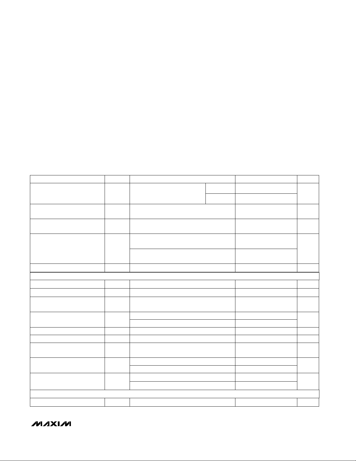
ELECTRICAL CHARACTERISTICS (continued)
(V+ = +5V ±5%, VDD= +2.7V to +5.25V, V
REFIN+
= +2.50V, REFIN- = AGND, f
CLKIN
= 2.4576MHz, TA= T
MIN
to T
MAX
, unless other-
wise noted. Typical values are at T
A
= +25°C.)
For specified performance V4.75 5.25V+V+ Voltage
V2.7 5.25V
DD
VDDVoltage
dB(Note 17)PSR
Power-Supply Rejection V+
(Note 16)
ANALOG POWER-SUPPLY CURRENT (Measured with digital inputs at either DGND or VDD, external CLKIN, burn-out and auxil-
iary currents disabled, X2CLK = 0, CLK = 0 for 1.024MHz, CLK = 1 for 2.4576MHz.)
DIGITAL POWER-SUPPLY CURRENT (Measured with digital inputs at either DGND or VDD, external CLKIN, burn-out and auxiliary
currents disabled, X2CLK = 0, CLK = 0 for 1.024MHz, CLK = 1 for 2.4576MHz.)
POWER REQUIREMENTS
Page 6
MAX1402
+5V, 18-Bit, Low-Power, Multichannel,
Oversampling (Sigma-Delta) ADC
6 _______________________________________________________________________________________
Note 1: Nominal gain is 0.98. This ensures a full-scale input voltage may be applied to the part under all conditions without caus-
ing saturation of the digital output data.
Note 2: Positive Full-Scale Error includes zero-scale errors (unipolar offset error or bipolar zero error) and applies to both unipolar
and bipolar input ranges. This error does not include the nominal gain of 0.98.
Note 3: Full-Scale Drift includes zero-scale drift (unipolar offset drift or bipolar zero drift) and applies to both unipolar and bipolar
input ranges.
Note 4: Gain Error does not include zero-scale errors. It is calculated as (full-scale error - unipolar offset error) for unipolar ranges
and as (full-scale error - bipolar zero error) for bipolar ranges. This error does not include the nominal gain of 0.98.
Note 5: Gain-Error Drift does not include unipolar offset drift or bipolar zero drift. It is effectively the drift of the part if zero-scale
error is removed.
Note 6: Use of the offset DAC does not imply that any input may be taken below AGND.
Note 7: Additional noise added by the offset DAC is dependent on the filter cutoff, gain, and DAC setting. No noise is added for a
DAC code of 0000.
Note 8: Guaranteed by design or characterization; not production tested.
Note 9: The absolute input voltage must be within the input-voltage range specification.
Note 10: All AIN and REFIN pins have identical input structures. Leakage is production tested only for the AIN3, AIN4, AIN5,
CALGAIN and CALOFF inputs.
Note 11: The dynamic load presented by the MAX1402 analog inputs for each gain setting is discussed in detail in the
Switching
Network
Section.Values are provided for the maximum allowable external series resistance.
2.4576MHz
1.024MHz
Buffers off
Buffers off
Buffers on
2.4576MHz
1.024MHz
2.43 3.6
Buffers off
Buffers off
Buffers on
Normal mode,
MF1 = 0,
MF0 = 0
4.23 5.75
2.43 3.75
Buffers on 3.7
Buffers on
2X mode,
MF1 = 0,
MF0 = 1
7.4 10
CONDITIONS
3.5 5.25
1.88
2.4576MHz
1.024MHz
Buffers off
Buffers off
Buffers on
2.4576MHz
1.024MHz
6.85
Buffers off
Buffers off
Buffers on
4X mode,
MF1 = 1,
MF0 = 0
25.8 33
10.8 14
Buffers on 25.2
Buffers on
8X mode,
MF1 = 1,
MF0 = 1
mW
26.7 34
PDPower Dissipation
11.7 15
10.2
2.95
(Note 18) 10 100 µWStandby Power Dissipation
1.45 2.55
UNITSMIN TYP MAXSYMBOLPARAMETER
ELECTRICAL CHARACTERISTICS (continued)
(V+ = +5V ±5%, VDD= +2.7V to +5.25V, V
REFIN+
= +2.50V, REFIN- = AGND, f
CLKIN
= 2.4576MHz, TA= T
MIN
to T
MAX
, unless other-
wise noted. Typical values are at T
A
= +25°C.)
4X mode,
MF1 = 1, MF0 = 0
mA
0.17
I
DD
5V Digital Supply Current
1.024MHz
2.4576MHz 0.36 0.6
8X mode,
MF1 = 1, MF0 = 1
0.241.024MHz
2.4576MHz 0.53 0.8
5V POWER DISSIPATION (V+ = VDD= +5V, digital inputs = 0 or VDD, external CLKIN, burn-out and auxiliary currents disabled,
X2CLK = 0, CLK = 0 for 1.024MHz, CLK = 1 for 2.4576MHz.)
Page 7
MAX1402
+5V, 18-Bit, Low-Power, Multichannel,
Oversampling (Sigma-Delta) ADC
_______________________________________________________________________________________ 7
TIMING CHARACTERISTICS
(V+ = +5V ±5%, VDD= +2.7V to +5.25V, AGND = DGND, f
CLKIN
= 2.4576MHz; input logic 0 = 0V; logic 1 = VDD, TA= T
MIN
to T
MAX
,
unless otherwise noted.) (Notes 19, 20, 21)
0 100VDD= 3.3V
VDD= 5V
Bus Relinquish Time After SCLK
Rising Edge (Note 26)
t
10
10 100
ns
VDD= 5V
SCLK Falling Edge to Data Valid
Delay (Notes 24, 25)
t
6
080
ns
INT High Time
t
INT
560 / N
· t
CLKIN
ns
X2CLK = 1, N = 2
(2 · MF1 + MF0)
Crystal oscillator or clock externally supplied for specified performance (Notes 22, 23)
SCLK Setup to Falling Edge CS
t
4
30 ns
SCLK Low Pulse Width t
8
100 ns
10 70
SCLK Rising Edge to INT High
(Note 27)
t
11
100VDD= 5V
CS Rising Edge to SCLK Rising
Edge Hold Time (Note 21)
t
9
0 ns
SCLK High Pulse Width t
7
100 ns
CS Falling Edge to SCLK Falling
Edge Setup Time
t
5
30 ns
280 / N
· t
CLKIN
INT to CS Setup Time (Note 8)
t
3
X2CLK = 0, N = 2
(2 · MF1 + MF0)
0 ns
RESET Pulse Width Low
t
2
100 ns
Master Clock Input Low Time f
CLKIN LO
0.4 ·
t
CLKIN
nst
CLKIN
= 1 / f
CLKIN
, X2CLK = 0
Master Clock Input High Time f
CLKIN HI
0.4 ·
t
CLKIN
nst
CLKIN
= 1 / f
CLKIN
, X2CLK = 0
Master Clock Frequency f
CLKIN
0.8 5.0
MHz
PARAMETER SYMBOL MIN TYP MAX UNITS
0.4 2.5
CONDITIONS
200
ns
X2CLK = 0
X2CLK = 1
VDD= 3.3V
VDD= 3.3V
Note 12: The input voltage range for the analog inputs is with respect to the voltage on the negative input of its respective differen-
tial or pseudo-differential pair. Table 5 shows which inputs form differential pairs.
Note 13: V
REF
= V
REFIN+
- V
REFIN-
.
Note 14: These specifications apply to CLKOUT only when driving a single CMOS load.
Note 15: The burn-out currents require a 500mV overhead between the analog input voltage and both V+ and AGND to operate cor-
rectly.
Note 16: Measured at DC in the selected passband. PSR at 50Hz will exceed 120dB with filter notches of 25Hz or 50Hz and FAST
bit = 0. PSR at 60Hz will exceed 120dB with filter notches of 20Hz or 60Hz and FAST bit = 0.
Note 17: PSR depends on gain. For a gain of +1V/V, PSR is 70dB typical. For a gain of +2V/V, PSR is 75dB typical. For a gain of
+4V/V, PSR is 80dB typical. For gains of +8V/V to +128V/V, PSR is 85dB typical.
Note 18: Standby power-dissipation and current specifications are valid only with CLKIN driven by an external clock and with the
external clock stopped. If the clock continues to run in standby mode, the power dissipation will be considerably higher.
30 nst
12
SCLK Setup to Falling Edge CS
SERIAL-INTERFACE READ OPERATION
SERIAL-INTERFACE WRITE OPERATION
Page 8
MAX1402
+5V, 18-Bit, Low-Power, Multichannel,
Oversampling (Sigma-Delta) ADC
8 _______________________________________________________________________________________
Note 19: All input signals are specified with tr= tf= 5ns (10% to 90% of VDD) and timed from a voltage level of 1.6V.
Note 20: See Figure 4.
Note 21: Timings shown in tables are for the case where SCLK idles high between accesses. The part may also be used with the
SCLK idling low between accesses, provided CS is toggled. In this case SCLK in the timing diagrams should be inverted
and the terms “SCLK Falling Edge” and “SCLK Rising Edge” exchanged in the specification tables. If CS is permanently
tied low, the part should only be operated with SCLK idling high between accesses.
Note 22: CLKIN duty cycle range is 45% to 55%. CLKIN must be supplied whenever the MAX1402 is not in standby mode. If no
clock is present, the device can draw higher current than specified.
Note 23: The MAX1402 is production tested with f
CLKIN
at 2.5MHz (1MHz for some IDDtests).
Note 24: Measured with the load circuit of Figure 1 and defined as the time required for the output to cross the V
OL
or VOHlimits.
Note 25: For read operations, SCLK active edge is falling edge of SCLK.
Note 26: Derived from the time taken by the data output to change 0.5V when loaded with the circuit of Figure 1. The number is then
extrapolated back to remove effects of charging or discharging the 50pF capacitor. This ensures that the times quoted in
the timing characteristics are true bus-relinquish times and are independent of external bus loading capacitances.
Note 27: INT returns high after the first read after an output update. The same data can be read again while INT is high, but be
careful not to allow subsequent reads to occur close to the next output update.
Note 28: Auxiliary inputs DS0 and DS1 are latched on the first falling edge of SCLK during a data-read cycle.
SCLK High Pulse Width t
16
100 ns
SCLK Low Pulse Width t
17
100 ns
Data Valid to SCLK Rising Edge
Hold Time
t
15
0 ns
PARAMETER SYMBOL MIN TYP MAX UNITS
CS Falling Edge to SCLK Falling
Edge Setup Time
t
13
30 ns
Data Valid to SCLK Rising Edge
Setup Time
t
14
30 ns
CONDITIONS
TIMING CHARACTERISTICS (continued)
(V+ = +5V ±5%, VDD= +2.7V to +5.25V, AGND = DGND, f
CLKIN
= 2.4576MHz; input logic 0 = 0V; logic 1 = VDD, TA= T
MIN
to T
MAX
,
unless otherwise noted.) (Notes 19, 20, 21)
CS Rising Edge to SCLK Rising
Edge Hold Time
t
18
0 ns
DS0/DS1 to SCLK Falling Edge
Hold Time (Notes 21 & 28)
t
20
0 ns
DS0/DS1 to SCLK Falling Edge
Setup Time (Notes 21 & 28)
t
19
40 ns
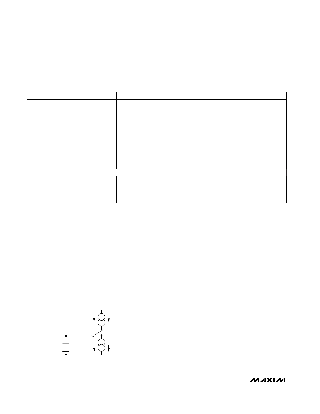
800µA
at V
DD
= +5V
100µA
at VDD = +3.3V
TO
OUTPUT
PIN
50pF
200µA
at V
DD
= +5V
100µA
at VDD = +3.3V
Figure 1. Load Circuit for Bus-Relinquish Time and VOLand
V
OH
Levels
AUXILIARY DIGITAL INPUTS (DS0 and DS1)
Page 9
MAX1402
+5V, 18-Bit, Low-Power, Multichannel,
Oversampling (Sigma-Delta) ADC
_______________________________________________________________________________________
9
0
50
100
150
200
250
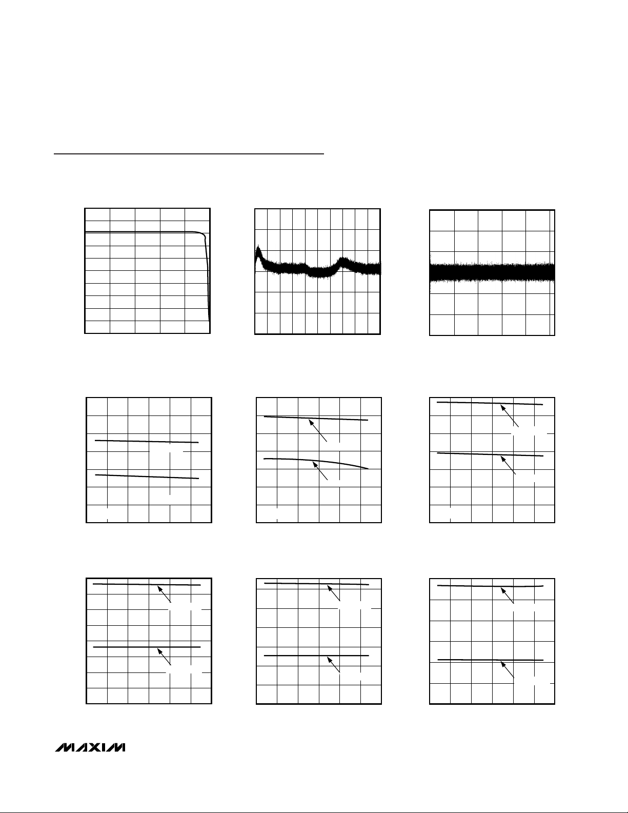
021 345
OUT1 AND OUT2 COMPLIANCE
MAX1402 toc01
COMPLIANCE VOLTAGE (V)
OUTPUT CURRENT (µA)
-15
0
-5
-10
5
10
15
-2.5 -0.5-1.0-2.0 -1.5 0 0.5 1.0 1.5 2.0 2.5
INTEGRAL NONLINEARITY AT 480sps,
GAIN = 1 (262, 144 pts)
MAX1402 toc12
DIFFERENTIAL INPUT VOLTAGE (V)
INL (ppm)
-15
0
-5
-10
5
10
15
0 0.5 1.0 1.5 2.0 2.5
MAX1402 toc13
CODE (x105)
DNL (ppm)
DIFFERENTIAL NONLINEARITY AT 480sps,
GAIN = 1 (262, 144 pts)
0
100
50
200
150
300
250
350
-50 0 25-25 50 75 100
VDD SUPPLY CURRENT vs. TEMPERATURE
(20sps OUTPUT DATA RATE UNBUFFERED)
MAX1402 toc02
TEMPERATURE (°C)
V
DD
SUPPLY CURRENT (µA)
VDD = +5.25V
V
DD
= +3.6V
(NOTE 29)
0
100
50
200
150
300
250
350
400
-50 0 25-25 50 75 100
V+ SUPPLY CURRENT vs. TEMPERATURE
(20sps OUTPUT DATA RATE)
MAX1402 toc07
TEMPERATURE (°C)
V+ SUPPLY CURRENT (µA)
BUFFERED
UNBUFFERED
0
100
50
200
150
300
250
350
-50 0 25-25 50 75 100
VDD SUPPLY CURRENT vs. TEMPERATURE
(60sps OUTPUT DATA RATE UNBUFFERED)
MAX1402 toc03
TEMPERATURE (°C)
V
DD
SUPPLY CURRENT (µA)
VDD = +5.25V
VDD = +3.6V
(NOTE 29)
0
100
50
200
150
300
250
350
-50 0 25-25 50 75 100
VDD SUPPLY CURRENT vs. TEMPERATURE
(120sps OUTPUT DATA RATE UNBUFFERED)
MAX1402 toc04
TEMPERATURE (°C)
V
DD
SUPPLY CURRENT (µA)
VDD = +5.25V
VDD = +3.6V
(NOTE 29)
0
200
100
400
300
600
500
-50 0 25-25 50 75 100
V+ SUPPLY CURRENT vs. TEMPERATURE
(60sps OUTPUT DATA RATE)
MAX1402 toc08
TEMPERATURE (°C)
V+ SUPPLY CURRENT (µA)
BUFFERED
UNBUFFERED
0
400
200
800
600
1200
1000
-50 0 25-25 50 75 100
V+ SUPPLY CURRENT vs. TEMPERATURE
(120sps OUTPUT DATA RATE)
MAX1402 toc09
TEMPERATURE (°C)
V+ SUPPLY CURRENT (µA)
BUFFERED
UNBUFFERED
Typical Operating Characteristics
(V+ = +5V, VDD= +5V, V
REFIN+
= +2.50V, REFIN- = AGND, f
CLKIN
= 2.4576MHz, TA= +25°C, unless otherwise noted.)
Page 10
MAX1402
+5V, 18-Bit, Low-Power, Multichannel,
Oversampling (Sigma-Delta) ADC
10 ______________________________________________________________________________________
0
100
50
250
200
150
400
350
300
450
-50 0-25 25 50 75 100
VDD SUPPLY CURRENT vs. TEMPERATURE
(240sps OUTPUT DATA RATE UNBUFFERED)
MAX1402 toc05
TEMPERATURE (°C)
V
DD
SUPPLY CURRENT (µA)
VDD = +5.25V
VDD = +3.6V
(NOTE 29)
0
200
100
400
300
600
500
-50 0 25-25 50 75 100
VDD SUPPLY CURRENT vs. TEMPERATURE
(480sps OUTPUT DATA RATE UNBUFFERED)
MAX1402 toc06
TEMPERATURE (°C)
V
DD
SUPPLY CURRENT (µA)
VDD = +5.25V
VDD = +3.6V
(NOTE 29)
0
2000
1000
4000
3000
5000
-50 0 25-25 50 75 100
V+ SUPPLY CURRENT vs. TEMPERATURE
(240sps OUTPUT DATA RATE)
MAX1402 toc10
TEMPERATURE (°C)
V+ SUPPLY CURRENT (µA)
BUFFERED
UNBUFFERED
0
2000
1000
4000
3000
5000
-50 0 25-25 50 75 100
V+ SUPPLY CURRENT vs. TEMPERATURE
(480sps OUTPUT DATA RATE)
MAX1402 toc11
TEMPERATURE (°C)
V+ SUPPLY CURRENT (µA)
BUFFERED
UNBUFFERED
Typical Operating Characteristics (continued)
(V+ = +5V, VDD= +5V, V
REFIN+
= +2.50V, REFIN- = AGND, f
CLKIN
= 2.4576MHz, TA= +25°C, unless otherwise noted.)
Note 29: Minimize capacitive loading at CLKOUT for lowest V
DD
supply current.
Typical Operating Characteristics
show V
DD
supply current with CLKOUT loaded by 120pF.
Page 11
MAX1402
+5V, 18-Bit, Low-Power, Multichannel,
Oversampling (Sigma-Delta) ADC
______________________________________________________________________________________ 11
Pin Description
15 AIN5
Analog Input Channel 5. Used as a differential or pseudo-differential input with AIN6
(see
Communications Register
section).
NAME FUNCTION
1 CLKIN
Clock Input. A crystal can be connected across CLKIN and CLKOUT. Alternatively, drive CLKIN with a
CMOS-compatible clock at a nominal frequency of 2.4576MHz or 1.024MHz, and leave CLKOUT unconnected. Frequencies of 4.9152MHz and 2.048MHz may be used if the X2CLK control bit is set to 1.
PIN
2 CLKOUT
Clock Output. When deriving the master clock from a crystal, connect the crystal between CLKIN and
CLKOUT. In this mode, the on-chip clock signal is not available at CLKOUT. Leave CLKOUT unconnected
when CLKIN is driven with an external clock.
3
CS
Chip-Select Input. Active-low logic input used to enable the digital interface. With CS hard-wired low, the
MAX1402 operates in its 3-wire interface mode with SCLK, DIN and DOUT used to interface to the device.
CS is used either to select the device in systems with more than one device on the serial bus, or as a
frame-synchronization signal for the MAX1402 when a continuous SCLK is used.
4
RESET
Active-Low Reset Input. Drive low to reset the control logic, interface logic, digital filter and analog modulator to power-on status. RESET must be high and CLKIN must be toggling in order to exit reset.
5 DS1
Digital Input for Auxiliary Data Input Bit 1. The status of this bit is reflected in the output data by bit D4.
Used to communicate the status of DS1 via the serial interface.
6 DS0
Digital Input for Auxiliary Data Input Bit 0. The status of this bit is reflected in the output data by bit D3.
Used to communicate the status of DS0 via the serial interface.
7 OUT2 Transducer Excitation Current Source 2
8 OUT1 Transducer Excitation Current Source 1
9 AGND Analog Ground. Reference point for the analog circuitry. AGND connects to the IC substrate.
10 V+ Analog Positive Supply Voltage (+4.75V to +5.25V).
11 AIN1
Analog Input Channel 1. May be used as a pseudo-differential input with AIN6 as common, or as the positive input of the AIN1/AIN2 differential analog input pair (see
Communications Register
section).
12 AIN2
Analog Input Channel 2. May be used as a pseudo-differential input with AIN6 as common, or as the negative input of the AIN1/AIN2 differential analog input pair (see
Communications Register
section).
13 AIN3
Analog Input Channel 3. May be used as a pseudo-differential input with AIN6 as common, or as the positive input of the AIN3/AIN4 differential analog input pair (see
Communications Register
section).
14 AIN4
Analog Input Channel 4. May be used as a pseudo-differential input with AIN6 as common, or as the negative input of the AIN3/AIN4 differential analog input pair (see
Communications Register
section).
16 AIN6
Analog Input 6. May be used as a common point for AIN1 through AIN5 in pseudo-differential mode, or as
the negative input of the AIN5/AIN6 differential analog input pair (see
Communications Register
section).
Page 12
MAX1402
+5V, 18-Bit, Low-Power, Multichannel,
Oversampling (Sigma-Delta) ADC
12 ______________________________________________________________________________________
Pin Description (continued)
NAME FUNCTIONPIN
17 CALGAIN-
Negative Gain Calibration Input. Used for system-gain calibration. It forms the negative input of a fully
differential input pair with CALGAIN+. Normally these inputs are connected to reference voltages in the
system. When system gain calibration is not required and the auto-sequence mode is used, the
CALGAIN+/CALGAIN- input pair provides an additional fully differential input channel.
18 CALGAIN+
Positive Gain Calibration Input. Used for system gain calibration. It forms the positive input of a fully differential input pair with CALGAIN-. Normally these inputs are connected to reference voltages in the system.
When system gain calibration is not required and the auto-sequence mode is used, the CALGAIN+/
CALGAIN- input pair provides an additional fully differential input channel.
19 REFIN-
Negative Differential Reference Input. Bias REFIN- between V+ and AGND, provided that REFIN+ is more
positive than REFIN-.
20 REFIN+
Positive Differential Reference Input. Bias REFIN+ between V+ and AGND, provided that REFIN+ is more
positive than REFIN-.
21 CALOFF-
Negative Offset Calibration Input. Used for system offset calibration. It forms the negative input of a fully
differential input pair with CALOFF+. Normally these inputs are connected to zero-reference voltages in
the system. When system offset calibration is not required and the auto-sequence mode is used, the
CALOFF+/CALOFF- input pair provides an additional fully differential input channel.
22 CALOFF+
Positive Offset Calibration Input. Used for system offset calibration. It forms the positive input of a fully
differential input pair with CALOFF-. Normally these inputs are connected to zero-reference voltages in the
system. When system offset calibration is not required and the auto-sequence mode is used, the
CALOFF+/CALOFF- input pair provides an additional fully differential input channel.
23 DGND Digital Ground. Reference point for digital circuitry.
24 V
DD
Digital Supply Voltage (+2.7V to +5.25V)
25
INT
Interrupt Output. A logic low indicates that a new output word is available from the data register. INT
returns high upon completion of a full output word read operation. INT also returns high for short periods
(determined by the filter and clock control bits) if no data read has taken place. A logic high indicates
internal activity, and a read operation should not be attempted under this condition. INT can also provide
a strobe to indicate valid data at DOUT (MDOUT = 1).
26 DOUT
Serial Data Output. DOUT outputs data from the internal shift register containing information from the
Communications Register, Global Setup Registers, Transfer Function Registers, or Data Register. DOUT
can also provide the digital bit stream directly from the Σ-∆ modulator (MDOUT = 1).
27 DIN
Serial Data Input. Data on DIN is written to the input shift register and later transferred to the
Communications Register, Global Setup Registers, Special Function Register, or Transfer Function
Registers, depending on the register selection bits in the Communications Register.
28 SCLK
Serial Clock Input. Apply an external serial clock to transfer data to and from the MAX1402. This serial
clock can be continuous, with data transmitted in a train of pulses, or intermittent. If CS is used to frame
the data transfer, then SCLK may idle high or low between conversions and CS determines the desired
active clock edge (see
Selecting Clock Polarity
). If CS is tied permanently low, SCLK must idle high
between data transfers.
Page 13

MAX1402
+5V, 18-Bit, Low-Power, Multichannel,
Oversampling (Sigma-Delta) ADC
______________________________________________________________________________________ 13
_______________Detailed Description
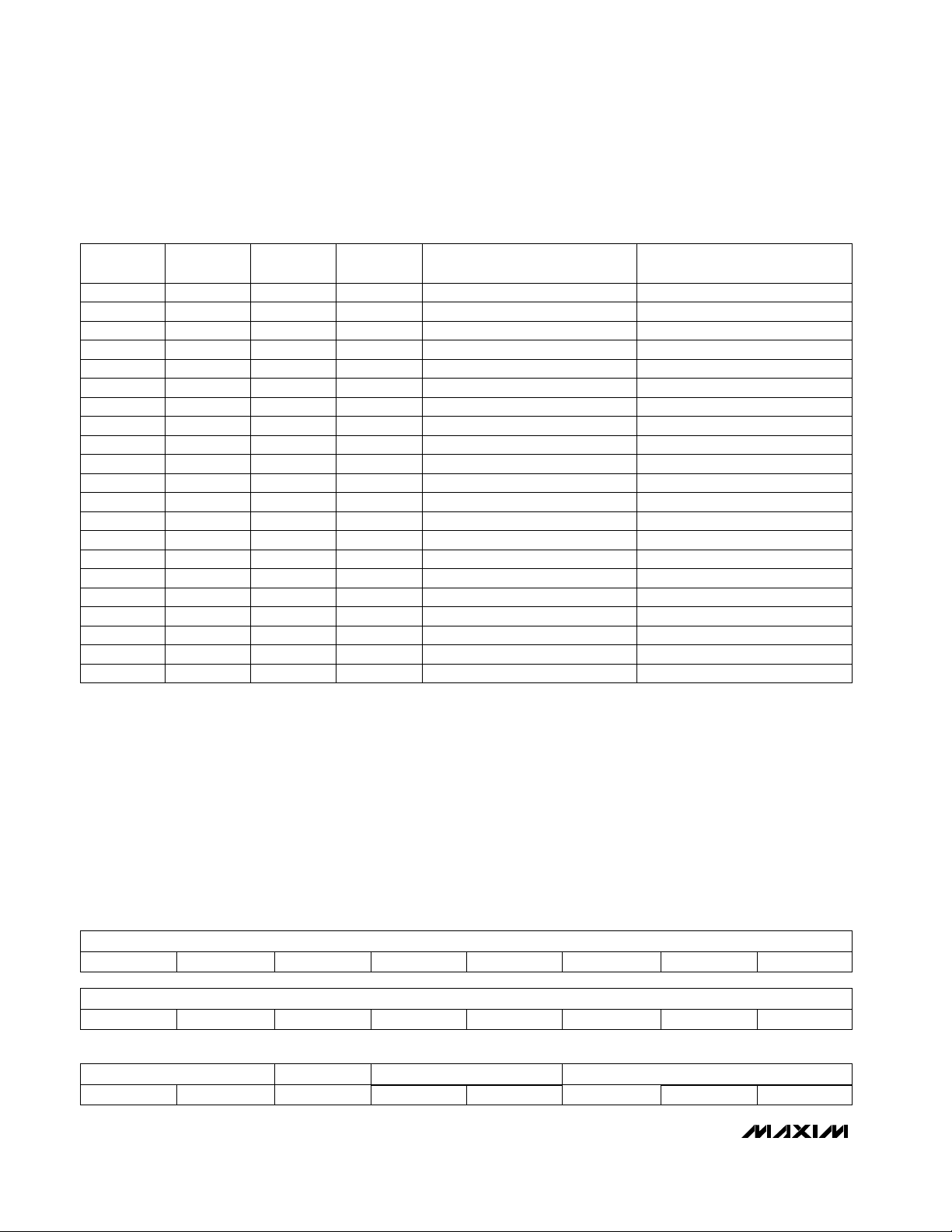
Circuit Description
The MAX1402 is a low-power, multichannel, serial-output,
sigma-delta ADC designed for applications with a wide
dynamic range, such as weigh scales and pressure
transducers. The functional block diagram in Figure 2
contains a switching network, a modulator, a PGA, two
buffers, an oscillator, an on-chip digital filter, and a
bidirectional serial communications port.
Three fully-differential input channels feed into the
switching network. Each channel may be independently programmed with a gain between +1V/V and
+128V/V. These three differential channels may also be
configured to operate as five pseudo-differential input
channels. Two additional, fully differential system-calibration channels allow system gain and offset error to
be measured. These system-calibration channels can
be used as additional differential signal channels when
dedicated gain and offset error correction channels are
not required.
Two chopper-stabilized buffers are available to isolate
the selected inputs from the capacitive loading of the
PGA and modulator. Three independent DACs provide
compensation for the DC component of the input signal
on each of the differential input channels.
The sigma-delta modulator converts the input signal into
a digital pulse train whose average duty cycle represents
the digitized signal information. The pulse train is then
processed by a digital decimation filter, resulting in a
conversion accuracy exceeding 16 bits. The digital filter’s
decimation factor is user-selectable, which allows the
conversion result’s resolution to be reduced to achieve a
higher output data rate. When used with 2.4576MHz or
1.024MHz master clocks, the decimation filter can be
programmed to produce zeros in its frequency response
at the line frequency and associated harmonics. This
ensures excellent line rejection without the need for further post-filtering. In addition, the modulator sampling
frequency can be optimized for either lowest power dissipation or highest output data rate.
AGND
V+
DGND
V
DD
CALOFF+
OUT2
OUT1
CALGAIN+
CALOFF-
CALGAIN-
AIN1
AIN2
AIN3
AIN4
AIN5
AIN6
SWITCHING
NETWORK
MODULATOR
DAC
PGA
V+
BUFFER
BUFFER
AGND
V+
DIGITAL
FILTER
SCLK
DIN
DOUT
INT
CS
DS0
DS1
RESET
CLKIN
CLKOUT
REFIN+
REFIN-
DIVIDER
MAX1402
INTERFACE
AND CONTROL
CLOCK
GEN
Figure 2. Functional Diagram
Page 14

MAX1402
+5V, 18-Bit, Low-Power, Multichannel,
Oversampling (Sigma-Delta) ADC
14 ______________________________________________________________________________________
The MAX1402 can be configured to sequentially scan
all signal inputs and to transmit the results through the
serial interface with minimum communications overhead. The output word contains a result identification
tag to indicate the source of each conversion result.
Serial Digital Interface
The serial digital interface provides access to eight onchip registers (Figure 3). All serial-interface commands
begin with a write to the communications register
(COMM). On power-up, system reset, or interface reset,
the part expects a write to its communications register.
The COMM register access begins with a 0 start bit.
The COMM register R/W bit selects a read or write
operation, and the register select bits (RS2, RS1, RS0)
select the register to be addressed. Hold DIN high
when not writing to COMM or another register (Table 1).
The serial interface consists of five signals: CS, SCLK,
DIN, DOUT, and INT. Clock pulses on SCLK shift bits
into DIN and out of DOUT. INT provides an indication
that data is available. CS is a device chip-select input
as well as a clock polarity select input (Figure 4). Using
CS allows the SCLK, DIN, and DOUT signals to be
shared among several SPI-compatible devices. When
short on I/O pins, connect CS low and operate the serial digital interface in CPOL = 1, CPHA = 1 mode using
SCLK, DIN, and DOUT. This 3-wire interface mode is
ideal for opto-isolated applications. Furthermore, a
microcontroller (such as a PIC16C54 or 80C51) can
use a single bidirectional I/O pin for both sending to
DIN and receiving from DOUT (see
Applications
Information
), because the MAX1402 drives DOUT only
during a read cycle.
Additionally, connecting the INT signal to a hardware
interrupt allows faster throughput and reliable, collisionfree data flow.
The MAX1402 features a mode where the raw modulator data output is accessible. In this mode the DOUT
and INT functions are reassigned (see the
Modulator
Data Output
section).
DATA REGISTER D1–D0/CID
RS0
GLOBAL SETUP REGISTER 1
GLOBAL SETUP REGISTER 2
SPECIAL FUNCTION REGISTER
XFER FUNCTION REGISTER 1
XFER FUNCTION REGISTER 2
XFER FUNCTION REGISTER 3
DATA REGISTER D17–D10
DATA REGISTER D9–D2
COMMUNICATIONS REGISTER
RS1RS2
DIN
DOUT
REGISTER
SELECT
DECODER
Figure 3. Register Summary
DIN
(DURING
WRITE)*
DOUT
(DURING
READ)*
DS1, DS0
MSB D6 D5 D4 D3 D2 D1 D0
MSB D6 D5 D4 D3 D2 D1 D0
CS
INT
t
10
t
6
t
20
t
19
t
8
t
7
t
17
t
16
t
3
t
1
t
13
t
5
t
4
t
12
t
18
t
9
t
11
t
15
t
14
SCLK
(CPOL = 1)
SCLK
(CPOL = 0)
*DOUT
IS HIGH IMPEDANCE DURING THE WRITE CYCLE; DIN IS IGNORED
DURING THE READ CYCLE.
Figure 4. Serial-Interface Timing
Table 1. Control Register Addressing
0
RS10RS0
0 1 Global Setup Register 10
1 0
1 1 Special Function Register0
Global Setup Register 2
Communications Register
0
0
0 0
0 1 Transfer Function Register 21
1 0
1 1 Data Register1
Transfer Function Register 3
Transfer Function Register 1
1
1
RS2 TARGET REGISTER
Page 15

MAX1402
+5V, 18-Bit, Low-Power, Multichannel,
Oversampling (Sigma-Delta) ADC
______________________________________________________________________________________ 15
Selecting Clock Polarity
The serial interface can be operated with the clock idling
either high or low. This is compatible with Motorola’s SPI
interface operated in CPOL = 1, CPHA = 1 or CPOL = 0,
CPHA = 1 mode. Select the clock polarity by sampling
the state of SCLK at the falling edge of CS. Ensure that
the setup times t4/t12and t5/t13are not violated. If CS is
connected to ground, resulting in no falling edge on CS,
SCLK must idle high (CPOL = 1, CPHA = 1).
Data-Ready Signal (DRDY bit true or
IINNTT
= low)
The data-ready signal indicates that new data may be
read from the 24-bit data register. After the end of a successful data register read, the data-ready signal
becomes false. If a new measurement completes before
the data is read, the data-ready signal becomes false.
The data-ready signal becomes true again when new
data is available in the data register.
The MAX1402 provides two methods of monitoring the
data-ready signal. INT provides a hardware solution
(active low when data is ready to be accessed), while
the DRDY bit in the COMM register provides a software
solution (active high).
Read data as soon as possible once data-ready
becomes true. This becomes increasingly important for
faster measurement rates. If the data-read is delayed
significantly, a collision may result. A collision occurs
when a new measurement completes during a dataregister read operation. After a collision, information in
the data register is invalid. The failed read operation
must be completed even though the data is invalid.
Resetting the Interface
Reset the serial interface by clocking in 32 1s.
Resetting the interface does not affect the internal registers.
If continuous data output mode is in use, clock in eight
0s followed by 32 1s. More than 32 1s may be clocked
in, since a leading 0 is used as the start bit for all operations.
Continuous Data Output Mode
When scanning the input channels (SCAN = 1), the serial interface allows the data register to be read repeatedly without requiring a write to the COMM register.
The initial COMM write (01111000) is followed by 24
clocks (DIN = high) to read the 24-bit data register.
Once the data register has been read, it can be read
again after the next conversion by writing another 24
clocks (DIN = high). Terminate the continuous data output mode by writing to the COMM register with any
valid access.
Modulator Data Output (MDOUT = 1)
Single-bit, raw modulator data is available at DOUT for
custom filtering when MDOUT = 1. INT provides a modulator clock for data synchronization. Data is valid on
the falling edge of INT. Write operations can still be
performed, however, read operations are disabled.
After MDOUT is returned to 0, valid data is accessed
by the normal serial-interface read operation.
On-Chip Registers
Communications Register
0/DRDY: (Default = 0) Data Ready Bit. On a write, this
bit must be reset to 0 to signal the start of the Communications Register data word. On a read, a 1 in this
location (0/DRDY) signifies that valid data is available in
the data register. This bit is reset after the data register
is read or, if data is not read, 0/DRDY will go low at the
end of the next measurement.
RS2, RS1, RS0: (Default = 0, 0, 0) Register Select
Bits. These bits select the register to be accessed
(Table 1).
R/W: (Default = 0) Read/Write Bit. When set high, the
selected register is read; when R/W = 0, the selected
register is written.
RESET: (Default = 0) Software Reset Bit. Setting this
bit high causes the part to be reset to its default powerup condition (RESET = 0).
STDBY: (Default = 0) Standby Power-Down Bit. Setting
the STDBY bit places the part in “standby” condition,
shutting down everything except the serial interface
and the CLK oscillator.
FSYNC: (Default = 0) Filter Sync Bit. When FSYNC = 0,
conversions are automatically performed at a data rate
determined by CLK, FS1, FS0, MF1, and MF0 bits.
When FSYNC = 1, the digital filter and analog modulator
First Bit (MSB) (LSB)
FUNCTION
0
STDBY
0
RESET
0
Name FSYNC
0
REGISTER SELECT BITS
RS0
0
RS1
0
DATA
RDY
Defaults
RS2
00
R/W
0/DRDY
Communications Register
Page 16

MAX1402
+5V, 18-Bit, Low-Power, Multichannel,
Oversampling (Sigma-Delta) ADC
16 ______________________________________________________________________________________
are held in reset, inhibiting normal self-timed operation.
This bit may be used to convert on command to minimize the settling time to valid output data, or to synchronize operation of a number of MAX1402s. FSYNC does
not reset the serial interface or the 0/DRDY flag. To clear
the 0/DRDY flag while FSYNC is active, simply read the
data register.
Global Setup Register 1
A1, A0: (Default = 0, 0) Channel-Selection Control Bits.
These bits (combined with the state of the DIFF, M1,
and M0 bits) determine the channel selected for conversion according to Tables 8, 9, and 10. These bits
are ignored if the SCAN bit is set.
MF1, MF0: (Default = 0, 0) Modulator Frequency Bits.
MF1 and MF0 determine the ratio of CLKIN oscillator frequency to modulator operating frequency. They affect
the output data rate, the position of the digital filter notch
frequencies, and the power dissipation of the device.
Achieve lowest power dissipation with MF1 = 0 and MF0
= 0. Highest power dissipation and fastest output data
rate occur with these bits set to 1, 1 (Table 2).
CLK: (Default = 1) CLK Bit. The CLK bit is used in conjunction with X2CLK to tell the MAX1402 the frequency
of the CLKIN input signal. If CLK = 0, a CLKIN input frequency of 1.024MHz (2.048MHz for X2CLK = 1) is
expected. If CLK = 1, a CLKIN input frequency of
2.4576MHz (4.1952MHz for X2CLK = 1) is expected.
This bit affects the decimation factor in the digital filter
and thus the output data rate (Table 2).
FS1, FS0: (Default = 0, 1) Filter Selection Bits. These
bits (in conjunction with the CLK bit) control the decimation ratio of the digital filter. They determine the output data rate, the position of the digital filter-frequency
response notches, and the noise present in the output
result. (Table 2).
FAST: (Default 0) FAST Bit. FAST = 0 causes the digital filter to perform a SINC
3
filter function on the modulator data stream. The output data rate will be determined by the values in the CLK, FS1, FS0, MF1, and
MF0 bits (Table 2). The settling time for SINC3 function
is 3 · [1 / (output data rate)]. In SINC3mode, the
MAX1402 automatically holds the DRDY signal false
(after any significant configuration change) until settled
data is available. FAST = 1 causes the digital filter to
perform a SINC1filter function on the modulator data
stream. The signal-to-noise ratio achieved with this filter
function is less than that of the SINC3filter; however
SINC1settles in a single output sample period, rather
than a minimum of three output sample periods for
SINC3. When switching from SINC1to SINC3mode, the
DRDY flag will be deasserted and reasserted after the
filter has fully settled. This mode change requires a
minimum of three samples.
Global Setup Register 2
SCAN: (Default = 0) Scan Bit. Setting this bit to a 1
causes sequential scanning of the input channels as
determined by DIFF, M1, and M0 (see
Scanning (Scan-
Mode)
). When SCAN = 0, the MAX1402 repeatedly
measures the unique channel selected by A1, A0,
DIFF, M1, and M0 (Table 4).
M1, M0: (Default 0, 0) Mode Control Bits. These bits
control access to the calibration channels CALOFF and
CALGAIN. When SCAN = 0, setting M1 = 0 and M0 = 1
selects the CALOFF input, and M1 = 1 and M0 = 0
selects the CALGAIN input (Table 3). When SCAN = 1
and M1 ≠ M0, the scanning sequence includes both
CALOFF and CALGAIN inputs (Table 4). When SCAN is
set to 1 and the device is scanning the available input
channels, selection of either calibration mode (01 or 10)
will cause the scanning sequence to be extended to
include a conversion on both the CALGAIN+
/CALGAIN- input pair and the CALOFF+/CALOFF- input
First Bit (MSB) (LSB)
First Bit (MSB) (LSB)
A1
CLK
0 1
A0
Defaults
CHANNEL SELECTION
0
MF1
0
MF0
MODULATOR
FREQUENCY
0
FASTName
0
FS1
0
FS0
FILTER SELECTION
1
FUNCTION
SCAN DIFF
0 0
M1
Defaults 0
M0
0
BUFF
MODE CONTROL
0
X2CLKName
0
BOUT
0
IOUT
0
FUNCTION
Global Setup Register 2
Global Setup Register 1
Page 17

CLK
MAX1402
+5V, 18-Bit, Low-Power, Multichannel,
Oversampling (Sigma-Delta) ADC
______________________________________________________________________________________ 17
pair. The exact sequence depends on the state of the
DIFF bit (Table 4). When scanning, the calibration
channels use the PGA gain, format, and DAC settings
defined by the contents of Transfer Function Register 3.
BUFF: (Default = 0) The BUFF bit controls operation of
the input buffer amplifiers. When this bit is 0, the internal buffers are bypassed and powered down. When
this bit is set high, the buffers drive the input sampling
capacitors and minimize the dynamic input load.
DIFF: (Default = 0) Differential/Pseudo-Differential Bit.
When DIFF = 0, the part is in pseudo-differential mode,
and AIN1–AIN5 are measured respective to AIN6, the
analog common. When DIFF = 1, the part is in differential mode with the analog inputs defined as AIN1/AIN2,
AIN3/AIN4, and AIN5/AIN6. The available input channels for each mode are tabulated in Table 5. Note that
DIFF also affects the scanning sequence when the part
is placed in SCAN mode (Table 4).
BOUT: (Default = 0) Burn-out Current Bit. Setting BOUT
= 1 connects 100nA current sources to the selected analog input channel. This mode is used to check that a
transducer has not burned out or opened circuit. The
burn-out current source must be turned off (BOUT = 0)
before measurement to ensure best linearity.
IOUT: (Default = 0) The IOUT bit controls the
Transducer Excitation Currents. A ‘0’ in this bit disables
OUT1 and OUT2 effectively making these pins highimpedance. A ‘1’ in this location activates both IOUT1
and IOUT2 causing each pin to source 200µA.
X2CLK: (Default = 0) Times-Two Clock Bit. Setting this
bit to 1 selects a divide-by-2 prescaler in the clock signal path. This allows use of a higher frequency crystal
or clock source and improves immunity to asymmetric
clock sources.
Table 2. Data Output Rate vs. CLK, Filter Select, and Modulator Frequency Bits
* Data rates offering noise-free 16-bit resolution.
Note: When FAST = 0, f
-3dB
= 0.262 ·Data Rate. When FAST = 1, f
-3dB
= 0.443 ·Data Rate.
Default condition is in bold print.
Table 3. Special Modes Controlled by M1, M0 (SCAN = 0)
DESCRIPTIONM1
0
1
Normal Mode: The device operates normally.
Calibrate Gain: In this mode the MAX1402 converts the voltage applied across CALGAIN+
and CALGAIN-. The PGA gain, DAC, and format settings of the selected channel (defined by
DIFF, A1, A0) are used.
1
Reserved: Do not use.
1
0
0
Calibrate Offset: In this mode the MAX1402 converts the voltage applied across CALOFF+
and CALOFF-. The PGA gain, DAC, and format settings of the selected channel (defined by
DIFF, A1, A0) are used.
1
M0
0
2400 4800400 480114.9152 12.4576
1200 2400200 240114.9152 02.4576
600 1200100 120014.9152 12.4576
300 60050
6001
4.9152
02.4576
800 1600160 200102.048 11.024
400 80080 100102.048 01.024
200 40040 50002.048 11.024
100
CLK MF1
X2CLK = 0
f
CLKIN
(MHz)
20020
MF0
2500
CLKIN
FREQ.
X2CLK = 1
f
CLKIN
(MHz)
2.048 0
CLKIN
FREQ.
1.024
FS1, FS0
(0, 0)
(sps)*
FS1, FS0
(0, 1)
(sps)*
FS1, FS0
(1, 0)
(sps)
FS1, FS0
(1, 1)
(sps)
AVAILABLE OUTPUT DATA RATES
Page 18

MAX1402
+5V, 18-Bit, Low-Power, Multichannel,
Oversampling (Sigma-Delta) ADC
18 ______________________________________________________________________________________
Special Function Register (Write-Only)
MDOUT: (Default = 0) Modulator Out Bit. MDOUT = 0
enables data readout on the DOUT pin, the normal condition for the serial interface. MDOUT = 1 changes the
function of the DOUT and INT pins, providing raw, single-bit modulator output instead of the normal serialdata interface output. This allows custom filtering
directly on the modulator output, without going through
the on-chip digital filter. The INT pin provides a clock to
indicate when the modulator data at DOUT should be
sampled (falling edge of INT). Note that in this mode,
the on-chip digital filter continues to operate normally.
When MDOUT is returned to 0, valid data may be
accessed through the normal serial-interface read
operation.
FULLPD: (Default = 0) Complete Power-Down Bit.
FULLPD = 1 forces the part into a complete power-down
condition, which includes the clock oscillator. The serial
interface continues to operate. The part requires a hardware reset to recover correctly from this condition.
Note: Changing the reserved bits in the special-function register from the default status of all 0s will select
one of the reserved modes and the part will not operate
as expected. This register is a write-only register.
However, in the event that this register is mistakenly
read, clock 24 bits of data out of the part to restore it to
the normal interface-idle state.
Transfer-Function Registers
The three transfer-function registers control the method
used to map the input voltage to the output codes. All
of the registers have the same format. The mapping of
control registers to associated channels depends on
the mode of operation and is affected by the state of
M1, M0, DIFF, and SCAN (Tables 8, 9, and 10).
Table 4. SCAN Mode Scanning
Sequences (SCAN = 1)
Table 5. Available Input Channels
(SCAN = 0)
Note: All other combinations reserved.
Special Function Register (Write-Only)
Transfer-Function Register
G2 D3
0 0Defaults
G1
PGA GAIN CONTROL
D0Name
OFFSET CORRECTION
0
D2
0 0
D1G0
00
U/B
0
FUNCTION
0
M10M0
0 1
AIN1–AIN6, AIN2–AIN6, AIN3–AIN6,
AIN4–AIN6, AIN5–AIN6, CALOFF,
CALGAIN
0
1 0
0 0 AIN1–AIN2, AIN3–AIN4, AIN5–AIN61
AIN1–AIN6, AIN2–AIN6, AIN3–AIN6,
AIN4–AIN6, AIN5–AIN6, CALOFF,
CALGAIN
AIN1–AIN6, AIN2–AIN6, AIN3–AIN6,
AIN4–AIN6, AIN5–AIN6
0
0
0 1
1 0
AIN1–AIN2, AIN3–AIN4, AIN5–AIN6,
CALOFF, CALGAIN
1
AIN1–AIN2, AIN3–AIN4, AIN5–AIN6,
CALOFF, CALGAIN
1
DIFF SEQUENCE
First Bit (MSB) (LSB)
0
0
0 0
0
Defaults
RESERVED BITS
0
MDOUT
0
0
0
FULLPDName
0
0
0
0
RESERVED BITS
0
FUNCTION
First Bit (MSB) (LSB)
0
M10M0
0 1 CALOFF0
1 0
0 0 AIN1–AIN2, AIN3–AIN4, AIN5–AIN61
CALGAIN
AIN1–AIN6, AIN2–AIN6,
AIN3–AIN6, AIN4–AIN6
0
0
0 1
1 0 CALGAIN1
CALOFF1
DIFF AVAILABLE CHANNELS
Page 19

MAX1402
+5V, 18-Bit, Low-Power, Multichannel,
Oversampling (Sigma-Delta) ADC
______________________________________________________________________________________ 19
Analog Inputs AIN1 to AIN6
Inputs AIN1 and AIN2 map to transfer-function register
1, regardless of scanning mode (SCAN = 1) or singleended vs. differential (DIFF) modes. Likewise, AIN3 and
AIN4 inputs always map to transfer-function register 2.
Finally, AIN5 always maps to transfer-function register 3
(input AIN6 is analog common).
CALGAIN and CALOFF
When not in scan mode (SCAN = 0), A1 and A0 select
which transfer function applies to CALGAIN and
CALOFF. In scan mode (SCAN = 1), CALGAIN and
CALOFF are always mapped to transfer-function register 3. Note that when scanning while M1 ≠ M0, the scan
sequence includes both CALGAIN and CALOFF channels (Table 4). CALOFF always precedes CALGAIN,
even though both channels share the same channel ID
tag (Table 11).
Note that changing the status of any active channel
control bits will cause INT to immediately transition high
and the modulator/filter to be reset. INT will reassert
after the appropriate digital-filter settling time. The control settings of the inactive channels may be changed
freely without affecting the status of INT or causing the
filter/modulator to be reset.
PGA Gain
Bits G2–G0 control the PGA gain according to Table 6.
Unipolar/Bipolar Mode
The U/B bit places the channel in either bipolar or
unipolar mode. A 0 selects bipolar mode, and a 1
selects unipolar mode. This bit does not affect the analog-signal conditioning. The modulator always accepts
bipolar inputs and produces a bitstream with 50%
ones-density when the selected inputs are at the same
potential. This bit controls the processing of the digitalfilter output, such that the available output bits are
mapped to the correct output range. Note U/B must be
set before a conversion is performed; it will not affect
any data already held in the output register.
Selecting bipolar mode does not imply that any input
may be taken below AGND. It simply changes the gain
and offset of the part. All inputs must remain within their
specified operating voltage range.
Offset-Correction DACs
Bits D3–D0 control the offset-correction DAC. The DAC
range depends on the PGA gain setting and is
expressed as a percentage of the available full-scale
input range (Table 7).
D3 is a sign bit, and D2–D0 represent the DAC magnitude. Note that when a DAC value of 0000 is programmed (the default), the DAC is disconnected from
the modulator inputs. This prevents the DAC from
degrading noise performance when offset correction is
not required.
Transfer-Function Register Mapping
Tables 8, 9, and 10 show the channel-control register
mapping in the various operating modes.
Table 6. PGA Gain Codes
Table 7. DAC Code vs. DAC Value
0
G1
0
G0
0 1 x20
1 0
1 1 x80
x4
x1
0
0
0 0
0 1 x321
1 0
1 1 x1281
x64
x16
1
1
G2 PGA GAIN
-66.7
-100
-116.7
-83.3
+66.7
+100
+116.7
UNIPOLAR
DAC VALUE
(% of FSR)
+83.3
DAC not connected
-33.3
-50
-16.7
DAC not connected
+33.3
+50
+16.7
1
0
1
0
1
0
1
0
1
0
1
0
1
0
1
D0
0
1
1
-33.3
-50
1 -58.311
11
1 -41.601
01
0
0
+33.3
+50
0 +58.311
11
0 +41.601
01
BIPOLAR
DAC VALUE
(% of FSR)
D3
1
1 -16.7
1 -2510
10
1 -8.300
00
0
0 +16.7
0 +2510
10
0 +8.300
D1
0
D2
0
Page 20

MAX1402
+5V, 18-Bit, Low-Power, Multichannel,
Oversampling (Sigma-Delta) ADC
20 ______________________________________________________________________________________
Table 8. Transfer-Function Register Mapping—Normal Mode (M1 = 0, M0 = 0)
3
2
3
1
1
3
TRANSFER
FUNCTION REG.
2
1
2
2
1
1
2
2
1
AIN5–AIN6
AIN3–AIN4
AIN5–AIN6
AIN1–AIN2
AIN1–AIN2
AIN5–AIN6
CHANNEL
AIN3–AIN4
AIN1–AIN6
AIN3–AIN6
AIN4–AIN6
AIN2–AIN6
AIN1–AIN6
AIN3–AIN6
AIN4–AIN6
AIN2–AIN6
X
X
X
X
0
1
0
X
X
X
X
1
0
1
A0
0
1
1
1 X1
X1
1 X1
X0
0
0 11
0
SCAN
01
01
1
1
1 X0
X0
1 X0
X0
0
0
0 10
10
0 00
A1
0
DIFF
0
Do Not Use11 11
Do Not Use10 11
X = Don’t care
Page 21

MAX1402
+5V, 18-Bit, Low-Power, Multichannel,
Oversampling (Sigma-Delta) ADC
______________________________________________________________________________________ 21
Table 9. Transfer-Function Register Mapping—Offset-Cal Mode (M1 = 0, M0 = 1)
X = Don’t care
AIN1–AIN6X1 1X0
AIN3–AIN4
CALOFF+ – CALOFF-
CALGAIN+ – CALGAIN-
AIN5–AIN6
X
X
X
X1
1
2
3
1 3X1
X1
1 3X1
X1
AIN5–AIN6
CALGAIN+ – CALGAIN-
AIN1–AIN2
CALOFF+ – CALOFF-
CALOFF+ – CALOFF-
CALOFF+ – CALOFF-
CHANNEL
CALOFF+ – CALOFF-
Do Not Use
AIN3–AIN6
AIN4–AIN6
AIN2–AIN6
CALOFF+ – CALOFF-
CALOFF+ – CALOFFCALOFF+ – CALOFF-
CALOFF+ – CALOFF-
X
X
X
X
0
1
0
X
X
X
1
1
0
1
A0
0
1
1
3
3
1 1X1
X0
1 3X0
X0
0
0
1
3
TRANSFER
FUNCTION REG.
11
0
SCAN
201
01
0
1 2
1 2X0
X0
1 1X0
11
0
0
1
2
0 210
10
0 100
A1
0
DIFF
0
Do Not Use11 11
Page 22
MAX1402
+5V, 18-Bit, Low-Power, Multichannel,
Oversampling (Sigma-Delta) ADC
22 ______________________________________________________________________________________
0
DIFF
0
A1
0 0 10
0 1
0 1 20
2
1
0
0
1 1
0 X 11
0 X
0 X 21
21
0
1 0
1 0 2
SCAN
0
1 1
TRANSFER
FUNCTION REG.
1 X
1 X
3
1
0
0
0 X
0 X 31
0 X
1 X 11
3
3
1
1
0
A0
1
0
1
1
X
X
X
0
1
0
3
X
X
X
X
CALGAIN+ – CALGAIN-
CALGAIN+ – CALGAIN-
CALGAIN+ – CALGAIN-
CALGAIN+ – CALGAIN-
AIN2–AIN6
AIN4–AIN6
AIN3–AIN6
Do Not Use
CALGAIN+ – CALGAIN-
CHANNEL
1
CALGAIN+ – CALGAIN-
CALGAIN+ – CALGAIN-
CALOFF+ – CALOFF-
AIN1–AIN2
CALGAIN+ – CALGAIN-
AIN5–AIN6
1 X
1 X 31
3
2
1
1 X
X
X
X
AIN5–AIN6
CALGAIN+ – CALGAIN-
CALOFF+ – CALOFF-
AIN3–AIN4
0 X 11 X AIN1–AIN6
1 11 1 Do Not Use
Table 10. Transfer-Function Register Mapping—Gain-Cal Mode (M1 = 1, M0 = 0)
Data Register (Read-Only)
The data register is a 24-bit, read-only register. Any
attempt to write data to this location will have no effect.
If a write operation is attempted, 8 bits of data must be
clocked into the part before it will return to its normal
idle mode, expecting a write to the communications
register.
Data is output MSB first, followed by one reserved 0 bit,
two auxiliary data bits, and a 3-bit channel ID tag indicating the channel from which the data originated.
D17–D0: The conversion result. D17 is the MSB. The
result is in offset binary format. 00 0000 0000 0000
0000 represents the minimum value and 11 1111 1111
1111 1111 represents the maximum value. Inputs
exceeding the available input range are limited to the
corresponding minimum or maximum output values.
0: This reserved bit will always be 0.
X = Don’t care
AUXILIARY DATA CHANNEL ID TAG
D1
DS0
D0 ‘0’
DS1 CID0
DATA BITS
CID2
CID1
RESERVED
(Data LSB) (LSB)
D9 D5D8 D7 D6 D2
DATA BITS
D4 D3
D17 D13D16 D15 D14 D10
DATA BITS
D12 D11
First Bit (Data MSB)
Data Register (Read-Only) Bits
Page 23

MAX1402
+5V, 18-Bit, Low-Power, Multichannel,
Oversampling (Sigma-Delta) ADC
______________________________________________________________________________________ 23
DS1, DS0: The status of the auxiliary data input pins.
These are latched on the first falling edge of the SCLK
signal for the current data register read access.
CID2–0: Channel ID tag (Table 11).
Switching Network
A switching network provides selection between three
fully differential input channels or five pseudo-differential channels, using AIN6 as a shared common. The
switching network provides two additional fully differential input channels intended for system calibration,
which may be used as extra fully differential signal
channels. Table 12 shows the channel configurations
available for both operating modes.
Scanning (SCAN-Mode)
To sample and convert the available input channels
sequentially, set the SCAN control bit in the global
setup register. The sequence is determined by DIFF
(fully differential or pseudo-differential) and by the
mode control bits M1 and M0 (Tables 8, 9, 10). With
SCAN set, the part automatically sequences through
each available channel, transmitting a single conversion result before proceeding to the next channel. The
MAX1402 automatically allows sufficient time for each
conversion to fully settle, to ensure optimum resolution
before asserting the data-ready signal and moving to
the next available channel. The scan rate is, therefore,
dependent on the clock bit (CLK), the filter control bits
(FS1, FS0), and the modulator frequency selection bits
(MF1, MF0).
Burn-Out Currents
The input circuitry also provides two “burn-out” currents. These small currents may be used to test the
integrity of the selected transducer. They can be selectively enabled or disabled by the BOUT bit in the global
setup register.
Transducer Excitation Currents
The MAX1402 provides two matched 200µA transducer
excitation currents at OUT1 and OUT2. These currents
have low absolute temperature coefficients and tight
Table 12. Input Channel Configuration in Fully and Pseudo-Differential Modes
(SCAN = 0)
X = Don’t care
*
This combination is available only in pseudo-differential mode when using the internal scanning logic
**
These combinations are only available in the calibration modes.
0
M0
0
DIFF
0 0 AIN20
0 0
0 0 AIN40
AIN3
AIN1
0
0
0 1
0 1 AIN30
0 1
1 X CALOFF+**0
AIN5
AIN1
0
0
0 X
1 X CALOFF+**
M1
0
0 X
HIGH INPUT
CALGAIN+**
AIN5*
1
0
0 X CALGAIN+**1
0
A1
0
1
1
0
0
1
X
X
X
X
X
MODE
Pseudo-
Differential
Fully
Differential
0
A0
1
0
1
0
1
0
X
X
X
X
X
AIN6
AIN6
AIN6
AIN6
AIN4
CALOFF-**
AIN6
AIN2
CALOFF-**
LOW INPUT
CALGAIN-**
AIN6*
CALGAIN-**
Table 11. Channel ID Tag Codes
Calibration
AIN5–AIN6
AIN3–AIN4
AIN1–AIN2
AIN4–AIN6
AIN3–AIN6
AIN2–AIN6
AIN1–AIN6
CHANNELCID0
0
1
0
1
0
1
0
11
1
0
0
1
1
0
0
CID1CID2
0
0
0
0
1
1
1
1
Page 24

MAX1402
+5V, 18-Bit, Low-Power, Multichannel,
Oversampling (Sigma-Delta) ADC
24 ______________________________________________________________________________________
TC matching. Optimized for transducer excitation, the
current sources possess tight temperature tracking
allowing accurate compensation of errors due to IR
drops in long transducer cable runs. They may be
enabled or disabled using a single register control bit
(IOUT).
Dynamic Input Impedance at the
Channel Selection Network
When used in unbuffered mode (BUFF = 0), the analog
inputs present a dynamic load to the driving circuitry.
The size of the sampling capacitor and the input sampling frequency (Figure 5) determine the dynamic load
seen by the driving circuitry. The MAX1402 samples at a
constant rate for all gain settings. This provides a maximum time for the input to settle at a given data rate. The
dynamic load presented by the inputs varies with the
gain setting. For gains of +2V/V, +4V/V, and +8V/V, the
input sampling capacitor increases with the chosen
gain. Gains of +16V/V, +32V/V, +64V/V, and +128V/V
present the same input load as the x8 gain setting.
When designing with the MAX1402, as with any other
switched-capacitor ADC input, consider the advantages
and disadvantages of series input resistance. A series
resistor reduces the transient-current impulse to the
external driving amplifier. This improves the amplifier
phase margin and reduces the possibility of ringing.
The resistor spreads the transient-load current from the
sampler over time due to the RC time constant of the
circuit. However, an improperly chosen series resistance can hinder performance in fast 16-bit converters.
The settling time of the RC network can limit the speed
at which the converter can operate properly, or reduce
the settling accuracy of the sampler. In practice, this
means ensuring that the RC time constant—resulting
from the product of the driving source impedance and
the capacitance presented by both the MAX1402’s
input and any external capacitances—is sufficiently
small to allow settling to the desired accuracy. Tables
13a–13d summarize the maximum allowable series
resistance vs. external capacitance for each MAX1402
gain setting in order to ensure 16-bit performance in
unbuffered mode.
R
EXT
C
EXT
R
MUX
C
PIN
R
SW
C
ST
C
SAMPLE
C
C
Figure 5. Analog Input, Unbuffered Mode (BUFF = 0)
Table 13a. R
EXT
, C
EXT
Values for Less than 16-Bit Gain Error in Unbuffered (BUFF = 0)
Mode—1x Modulator Sampling Frequency (MF1, MF0 = 00); X2CLK = 0; CLKIN = 2.4576MHz
Table 13b. R
EXT
, C
EXT
Values for Less than 16-Bit Gain Error in Unbuffered (BUFF = 0)
Mode—2x Modulator Sampling Frequency (MF1, MF0 = 01); X2CLK = 0; CLKIN =
2.4576MHz
45 20
45 20 132
34 17
22 13 9.7
8, 16, 32,
64, 128
12
13
4
1
C
EXT
= 0pF C
EXT
= 50pF C
EXT
= 100pF
3.9 2.2
3.9 2.2 0.58
3.6 2.0
3.3 1.9 0.49
0.53
PGA GAIN
0.58
C
EXT
= 50pF C
EXT
= 1000pF C
EXT
= 5000pF
EXTERNAL RESISTANCE R
EXT
(kΩ)
23 9.9
23 9.9 6.52
17 8.5
11.2 6.7 4.9
8, 16, 32,
64, 128
5.8
6.5
4
1
C
EXT
= 0pF C
EXT
= 50pF C
EXT
= 100pF
1.9 1.1
1.9 1.1 0.29
1.8 1.0
1.6 0.93 0.24
0.27
PGA GAIN
0.29
C
EXT
= 500pF C
EXT
= 1000pF C
EXT
= 5000pF
EXTERNAL RESISTANCE R
EXT
(kΩ)
Page 25

MAX1402
+5V, 18-Bit, Low-Power, Multichannel,
Oversampling (Sigma-Delta) ADC
______________________________________________________________________________________ 25
Input Buffers
The MAX1402 provides a pair of input buffers to isolate
the inputs from the capacitive load presented by the
PGA/modulator (Figure 6). The buffers are chopper stabilized to reduce the effect of their DC offsets and lowfrequency noise. Since the buffers can represent more
than 50% of the total analog power dissipation, they may
be shut down in applications where minimum power dissipation is required and the capacitive input load is not a
concern. Disable the buffers in applications where the
inputs must operate close to AGND or V+.
When used in buffered mode, the buffers isolate the
inputs from the sampling capacitors. The samplingrelated gain error is dramatically reduced in this mode.
A small dynamic load remains from the chopper stabilization. The multiplexer exhibits a small input leakage
current of up to 10nA. With high source resistances,
this leakage current may result in a DC offset.
Reference Input
The MAX1402 is optimized for ratiometric measurements and includes a fully differential reference input.
Apply the reference voltage across REFIN+ and REFIN-,
Table 13c. R
EXT
, C
EXT
Values for Less than 16-Bit Gain Error in Unbuffered (BUFF = 0)
Mode—4x Modulator Sampling Frequency (MF1, MF0 = 10 ); X2CLK = 0; CLKIN =
2.4576MHz
Table 13d. R
EXT
, C
EXT
Values for Less than 16-Bit Gain Error in Unbuffered (BUFF = 0)
Mode—8x Modulator Sampling Frequency (MF1, MF0 = 11); X2CLK = 0; CLKIN =
2.4576MHz
R
EXT
C
EXT
R
MUX
C
PIN
R
IN
C
ST
C
AMP
C
SAMPLE
C
C
Figure 6. Analog Input, Buffered Mode (BUFF = 1)
11.1 4.9
11.1 4.9 3.22
8.3 4.2
5.5 3.3 2.4
8, 16, 32,
64, 128
2.9
3.2
4
1
C
EXT
= 0pF C
EXT
= 50pF C
EXT
= 100pF
0.95 0.54
0.95 0.54 0.14
0.89 0.50
0.81 0.46 0.12
0.13
PGA GAIN
0.14
C
EXT
= 500pF C
EXT
= 1000pF C
EXT
= 5000pF
EXTERNAL RESISTANCE R
EXT
(kΩ)
5.4 2.4
5.4 2.4 1.62
4.0 2.1
2.7 1.6 1.2
8, 16, 32,
64, 128
1.4
1.6
4
1
C
EXT
= 0pF C
EXT
= 50pF C
EXT
= 100pF
0.47 0.26
0.47 0.26 0.069
0.43 0.25
0.39 0.23 0.059
0.064
PGA GAIN
0.069
C
EXT
= 500pF C
EXT
= 1000pF C
EXT
= 5000pF
EXTERNAL RESISTANCE R
EXT
(kΩ)
Page 26

MAX1402
+5V, 18-Bit, Low-Power, Multichannel,
Oversampling (Sigma-Delta) ADC
26 ______________________________________________________________________________________
ensuring that REFIN+ is more positive than REFIN-.
REFIN+ and REFIN- must be between AGND and V+.
The MAX1402 is specified with a +2.5V reference when
operating with a +5V analog supply (V+).
Modulator
The MAX1402 performs analog-to-digital conversion
using a single-bit, second-order, switched-capacitor
modulator. A single comparator within the modulator
quantizes the input signal at a much higher sample rate
than the bandwidth of the signal to be converted. The
quantizer then presents a stream of 1s and 0s to the
digital filter for processing, to remove the frequencyshaped quantization noise.
The MAX1402 modulator provides 2nd-order frequency
shaping of the quantization noise resulting from the single bit quantizer. The modulator is fully differential for
maximum signal-to-noise ratio and minimum susceptibility to power-supply noise.
The modulator operates at one of a total of eight different sampling rates (fM) determined by the master clock
frequency (f
CLKIN
), the X2CLK bit, the CLK bit, and the
modulator frequency control bits MF1 and MF0. Power
dissipation is optimized for each of these modes by
controlling the bias level of the modulator. Table 15
shows the input and reference sample rates.
PGA
A programmable gain amplifier (PGA) with a userselectable gain of x1, x2, x4, x8, x16, x32, x64, or x128
(Table 6) precedes the modulator. Figure 7 shows the
default bipolar transfer function with the following illustrated codes: 1) PGA = 0, DAC = 0; 2) PGA = 3, DAC =
0; or 3) PGA = 3, DAC = 3.
Output Noise
Tables 16a and 16b show the rms noise for typical output frequencies (notches) and -3dB frequencies for the
MAX1402 with f
CLKIN
= 2.4576MHz. The numbers
given are for the bipolar input ranges with V
REF
=
+2.50V, with no buffer (BUFF = 0) and with the buffer
inserted (BUFF = 1). These numbers are typical and
are generated at a differential analog input voltage of 0.
Figure 8 shows graphs of Effective Resolution vs. Gain
and Notch Frequency. The effective resolution values
were derived from the following equation:
Table 14. R
EXT
, C
EXT
Values for Less than 16-Bit Gain Error in Buffered (BUFF = 1)
Mode—All Modulator Sampling Frequencies (MF1, MF0 = XX); X2CLK = 0; CLKIN =
2.4576MHz
10 10
10 10 102
10 10 10
10
4
1
C
EXT
= 0pF C
EXT
= 50pF C
EXT
= 100pF
10 10
10 10 10
10 10 10
PGA GAIN
10
C
EXT
= 500pF C
EXT
= 1000pF C
EXT
= 5000pF
EXTERNAL RESISTANCE R
EXT
(kΩ)
10 10
10 10 1016
10 10 10
10
32
8 10 10
10 10 10
10 10 10
10
10 10 1064
10 10 10128
10 10 10
10 10 10
Figure 7. Effect of PGA and DAC Codes on the Bipolar
Transfer Function
FULL-SCALE 259522
CODE
MAX CODE 262144
MIDSCALE 131072
ZERO-SCALE 2621
PGA = 3
DAC = +3
/16
REF
AGND
-)-V
AIN
(V
INPUT VOLTAGE RANGE
REF
/8 - V
REF
-) - V
AIN
(V
/8
REF
-) - V
AIN
(V
PGA = 3
DAC = 0
PGA = 0
DAC = 0
NEGATIVE DAC STEP
SHIFTS THE TRANSFER
FUNCTION TOWARD
THE POSITIVE RAIL.
)
/8
/16
AIN-
REF
REF
(V
-) + V
/8 - V
AIN
REF
(V
-) - V
AIN
(V
REF
-) + V
AIN
(V
V+
Page 27

MAX1402
+5V, 18-Bit, Low-Power, Multichannel,
Oversampling (Sigma-Delta) ADC
______________________________________________________________________________________ 27
Table 15. Modulator Operating Frequency, Sampling Frequency, and 16-Bit Data
Output Rates
1
0
MF0
1
0
0
1
1
0
1
1
MF1
0
0
1
0
1
0
400, 480153.6307.2
200, 24076.8153.6
2.4576 14.9152
2.4576 14.9152
160, 200
100, 12038.4
AVAILABLE
OUTPUT
DATA RATES
AT 16-BIT
ACCURACY
(sps)
MOD.
FREQ.
f
M
(kHz)
AIN/REFIN
SAMPLING
FREQ.
f
S
(kHz)
76.8
50, 60
19.2
20, 25
80, 100
38.4
64128
32
1.024
64
2.4576
40, 501632
816
MCLK
FREQ.
X2CLK = 0
DEFAULT
f
CLKIN
(MHz)
CLK
MCLK
FREQ.
X2CLK = 1
f
CLKIN
(MHz)
14.9152
1.024
1.024
2.4576 1
4.9152
02.048
1.024 02.048
0
0
2.048
2.048
Table 16a. MAX1402 Noise vs. Gain and Output Data Rate—Unbuffered Mode,
V
REF
= 2.5V, f
CLKIN
= 2.4576MHz
PROGRAMMABLE GAIN
x1
x2 x4 x8 x16 x32 x64 x128
MF1:MF0 = 0
FS1:FS0 = 37.6813.9626.4751.42103.78203.74419.17820.7312584800
FS1:FS0 = 23.123.615.149.6718.9236.5469.17150.09628.82400
FS1:FS0 = 11.211.221.231.281.442.363.848.15125.7480
FS1:FS0 = 01.08
1.131.091.161.312.063.506.87104.8
400
MF1:MF0 = 3
FS1:FS0 = 37.38
13.8826.5751.17103.04200.51399.44816.66628.82400
FS1:FS0 = 22.793.385.209.4518.1135.9171.25141.69314.41200
FS1:FS0 = 11.091.091.141.151.342.044.167.0062.9240
FS1:FS0 = 01.01
0.981.021.071.261.964.006.2552.4
200
MF1:MF0 = 2
FS1:FS0 = 37.31
13.4024.5052.3899.75203.35405.49836.32314.41200
FS1:FS0 = 22.763.295.159.3419.1937.6973.86138.79157.2600
FS1:FS0 = 11.101.081.081.171.362.143.937.9131.4120
FS1:FS0 = 01.00
0.981.041.101.241.943.616.9826.2
100
MF1:MF0 = 1
FS1:FS0 = 37.43
13.2626.2550.91107.06216.88417.07844.82157.2600
FS1:FS0 = 22.753.545.059.5717.9135.1070.73147.6078.6300
FS1:FS0 = 11.101.101.121.201.362.213.947.2315.760
FS1:FS0 = 0
BIT
STATUS
0.99
TYPICAL OUTPUT NOISE IN µV
RMS
1.051.101.131.252.023.276.20
OUTPUT
DATA
RATE
(sps)
13.150
-3dB
FREQ.
(Hz)
Note: Default condition is in bold print.
Page 28

MAX1402
+5V, 18-Bit, Low-Power, Multichannel,
Oversampling (Sigma-Delta) ADC
28 ______________________________________________________________________________________
Table 16b. MAX1402 Noise vs. Gain and Output Data Rate—Buffered Mode,
V
REF
= 2.5V, f
CLKIN
= 2.4576MHz
PROGRAMMABLE GAIN
x1
x2 x4 x8 x16 x32 x64 x128
MF1:MF0 = 0
FS1:FS0 = 37.8913.5926.0752.48102.18205.60394.00803.8712584800
FS1:FS0 = 37.97
13.3325.7152.98105.18202.57408.09851.32628.8
2400
FS1:FS0 = 23.023.645.269.9218.0836.8073.71148.57314.41200
FS1:FS0 = 11.251.221.291.351.472.243.897.4062.9240
FS1:FS0 = 01.10
1.161.161.241.351.923.216.5552.4
200
MF1:MF0 = 2
FS1:FS0 = 37.87
13.5026.7752.39101.39201.87408.48830.30314.41200
FS1:FS0 = 23.413.925.489.3217.7736.0469.52143.45157.2600
FS1:FS0 = 11.461.451.491.451.642.534.128.3731.4120
FS1:FS0 = 23.213.795.459.5217.3635.9268.92144.96628.82400
FS1:FS0 = 11.311.301.341.401.582.284.147.58125.7480
FS1:FS0 = 01.21
1.171.211.281.382.213.836.60104.8
400
MF1:MF0 = 3
FS1:FS0 = 01.35
1.341.311.341.522.253.668.1026.2
100
MF1:MF0 = 1
FS1:FS0 = 37.78
13.7525.8550.28102.14195.95405.95823.33157.2600
FS1:FS0 = 23.524.105.609.3518.3235.6571.62142.0278.6300
FS1:FS0 = 11.481.491.531.491.642.544.247.1115.760
FS1:FS0 = 0
BIT
STATUS
1.39
TYPICAL OUTPUT NOISE IN µV
RMS
1.371.321.401.502.35
OUTPUT
DATA
RATE
(sps)
4.136.0513.150
-3dB
FREQ.
(Hz)
10
12
11
14
13
16
15
17
19
18
20
1482 163264128
GAIN (V/V)b) BUFF = 1a) BUFF = 0
EFFECTIVE RESOLUTION (BITS)
10
12
11
14
13
16
15
17
19
18
20
1482 163264128
GAIN (V/V)
EFFECTIVE RESOLUTION (BITS)
FS1: FS0 = 0 OR 1
FS1: FS0 = 2
FS1: FS0 = 3
CLK = 1
FS1: FS0 = 0 OR 1
FS1: FS0 = 2
FS1: FS0 = 3
CLK = 1
BUFF = 1
CLK = 1
BUFF = 0
Figure 8. Effective Resolution vs. Gain and Notch Frequency
Effective Resolution = (SNRdB- 1.76dB) / 6.02
The maximum possible signal divided by the noise of
the device, SNRdB, is defined as the ratio of the input
full-scale voltage (i.e., 2 · V
REFIN
/ GAIN) to the output
rms noise. Note that it is not calculated using peak-to-
peak output noise numbers. Peak-to-peak noise numbers can be up to 6.6 times the rms numbers, while
effective resolution numbers based on peak-to-peak
noise can be 2.5 bits below the effective resolution
based on rms noise, as quoted in the tables.
Page 29

MAX1402
+5V, 18-Bit, Low-Power, Multichannel,
Oversampling (Sigma-Delta) ADC
______________________________________________________________________________________ 29
The noise shown in Table 16 is composed of device
noise and quantization noise. The device noise is relatively low, but becomes the limiting noise source for
high gain settings. The quantization noise is dependent
on the notch frequency and becomes the dominant
noise source as the notch frequency is increased.
Offset-Correction DAC
The MAX1402 provides a coarse (3-bit plus sign) offsetcorrection DAC at the modulator input. Use this DAC to
remove the offset component in the input signal, allowing the ADC to operate on a more sensitive range. The
DAC offsets up to ±116.7% of the selected range in
±16.7% increments for unipolar mode and up to
±58.3% of the selected range in ±8.3% increments for
bipolar mode. When a DAC value of 0 is selected, the
DAC is completely disconnected from the modulator
inputs and does not contribute any noise. Figures 7
and 9 show the effect of the DAC codes on the input
range and transfer function.
Clock Oscillator
The clock oscillator may be used with an external crystal
(or resonator) connected between CLKIN and CLKOUT,
or may be driven directly by an external oscillator at
CLKIN with CLKOUT left unconnected. In normal operating mode, the MAX1402 is specified for operation with
CLKIN at either 1.024MHz (CLK = 0) or 2.4576MHz
(CLK = 1, default). When operated at these frequencies,
the part may be programmed to produce frequency
response nulls at the local line frequency (either 60Hz or
50Hz) and the associated line harmonics.
In standby mode (STBY = 1) all circuitry, with the
exception of the serial interface and the clock oscillator,
is powered down. The interface consumes minimal
power with a static SCLK. Enter power-down mode
(including the oscillator) by setting the FULLPD bit in
the special-function register. When exiting a full-power
shutdown, perform a hardware reset or a software reset
after the master clock signal is established (typically
10ms when using the on-board oscillator with an external crystal) to ensure that any potentially corrupted registers are cleared.
It is often helpful to use higher-frequency crystals or
resonators, especially for surface-mount applications
where the result may be reduced PC board area for the
oscillator component and a lower price or better component availability. Also, it may be necessary to operate the part with a clock source whose duty cycle is not
close to 50%. In either case, the MAX1402 can operate
with a master clock frequency of up to 5MHz, and
includes an internal divide-by-2 prescaler to restore the
internal clock frequency to a range of up to 2.5MHz
with a 50% duty cycle. To activate this prescaler, set
the X2CLK bit in the control registers. Note that using
CLKIN frequencies above 2.5MHz in combination with
the X2CLK mode will result in a small increase in digital
supply current.
Digital Filter
The on-chip digital filter processes the 1-bit data
stream from the modulator using a SINC3or SINC1filter. The SINC filters are conceptually simple, efficient,
and extremely flexible, especially where variable resolution and data rates are required. Also, the filter notch
positions are easily controlled, since they are directly
related to the output data rate (1 / data word period).
The SINC1function results in a faster settling response
while retaining the same frequency response notches
as the default SINC3filter. This allows the filter to settle
faster at the expense of resolution and quantization
noise. The SINC1filter settles in one data word period.
With 60Hz notches (60Hz data rate), the settling time
would be 1 / 60Hz or 16.7ms whereas the SINC3filter
would settle in 3 / 60Hz or 50ms. Toggle between these
filter responses using the FAST bit in the global setup
register. Use SINC1mode for faster settling and switch
to SINC3mode when full accuracy is required. Switch from
the SINC1to SINC3mode by resetting the FAST bit low.
The DRDY signal will go false and will be reasserted
DAC CODE
D3:
D2:
D1:
D0:
INPUT VOLTAGE RANGE
(V
REF = 2.5V
PGA = 000)
(V
REF = 1.25V
PGA = 000)
-7
1
1
1
1
-6
1
1
1
0
-5
1
1
0
1
-4
1
1
0
0
-3
1
0
1
1
-2
1
0
1
0
-1
1
0
1
0
0
0
0
0
0
+1
0
0
0
1
+2
0
0
1
0
+3
0
0
1
1
+4
0
1
0
0
+5
0
1
0
1
+6
0
1
1
0
+7
0
1
1
1
2.708V
2.50V
2.292V
2.083V
1.875V
1.667V
1.458V
1.25V
1.042V
0.833V
0.625V
0.416V
0.208V
0V
-0.208V
-0.416V
-0.625V
-0.833V
-1.042V
-1.25V
-1.458V
-1.667V
-1.875V
-2.083V
-2.292V
-2.50V
-2.708V
13/6 V
REF
/2
PGA
2 V
REF
/2
PGA
11/6 V
REF
/2
PGA
10/6 V
REF
/2
PGA
9/6 V
REF
/2
PGA
8/6 V
REF
/2
PGA
7/6 V
REF
/2
PGA
V
REF
/2
PGA
5/6 V
REF
/2
PGA
4/6 V
REF
/2
PGA
3/6 V
REF
/2
PGA
2/6 V
REF
/2
PGA
1/6 V
REF
/2
PGA
0
-1/6 V
REF
/2
PGA
-2/6 V
REF
/2
PGA
-3/6 V
REF
/2
PGA
-4/6 V
REF
/2
PGA
-5/6 V
REF
/2
PGA
-V
REF
/2
PGA
-7/6 V
REF
/2
PGA
-8/6 V
REF
/2
PGA
-9/6 V
REF
/2
PGA
-10/6 V
REF
/2
PGA
-11/6 V
REF
/2
PGA
-2 V
REF
/2
PGA
-13/6 V
REF
/2
PGA
5.00V
4.503V
4.167V
3.750V
3.333V
2.917V
2.50V
2.083V
1.667V
1.25V
0.833V
0.416V
0V
-0.416V
-0.833V
-1.25V
-1.667V
-2.083V
-2.50V
-2.917V
-3.333V
-3.750V
-4.167V
-4.503V
-5.00V
MAXIMUM INPUT
MINIMUM INPUT (U/B = 1)
MINIMUM INPUT (U/B = 0)
Figure 9. Input Voltage Range vs. DAC Code
Page 30

when valid data is available, a minimum of three dataword periods later.
The digital filter can be bypassed by setting the MDOUT
bit in the global setup register. When MDOUT = 1, the
raw output of the modulator is directly available at DOUT.
Filter Characteristics
The MAX1402 digital filter implements both a SINC
1
(sinx/x) and SINC3(sinx/x)3lowpass filter function. The
transfer function for the SINC3function is that of three
cascaded SINC1filters described in the z-domain by:
and in the frequency domain by:
where N, the decimation factor, is the ratio of the modulator frequency fMto the output frequency fN.
Figure 10 shows the filter frequency response. The
SINC3characteristic cutoff frequency is 0.262 times the
first notch frequency. This results in a cutoff frequency
of 15.72Hz for a first filter notch frequency of 60Hz. The
response shown in Figure 10 is repeated at either side
of the digital filter’s sample frequency (fM) and at either
side of the related harmonics (2fM, 3fM, . . .).
The response of the SINC3filter is similar to that of a
SINC1(averaging filter) filter but with a sharper rolloff.
The output data rate for the digital filter corresponds
with the positioning of the first notch of the filter’s frequency response. Therefore, for the plot of Figure 10
where the first notch of the filter is at 60Hz, the output
data rate is 60Hz. The notches of this (sinx/x)3filter are
repeated at multiples of the first notch frequency. The
SINC3filter provides an attenuation of better than
100dB at these notches.
Determine the cutoff frequency of the digital filter by the
value loaded into CLK, X2CLK, MF1, MF0, FS1, and FS0
in the global setup register. Programming a different
cutoff frequency with FS0 and FS1 does not alter the
profile of the filter response; it changes the frequency of
the notches. For example, Figure 11 shows a cutoff frequency of 13.1Hz and a first notch frequency of 50Hz.
For step changes at the input, a settling time must be
allowed before valid data can be read. The settling time
depends upon the output data rate chosen for the filter.
The settling time of the SINC
3
filter to a full-scale step
input can be up to four times the output data period.
For a synchronized step input (using the FSYNC function or the internal scanning logic), the settling time is
three-times the output data period.
H(f)
1
N
sin N
f
f
sin
f
f
M
M
3
=
π
π
H(z)
1N 1 z
1 – z
N
1
3
=
−
−
−
MAX1402
+5V, 18-Bit, Low-Power, Multichannel,
Oversampling (Sigma-Delta) ADC
30 ______________________________________________________________________________________
-160
-140
-100
-120
-80
-60
-20
-40
0
0 40608020 100 120 140 160 180 200
FREQUENCY (Hz)
GAIN (dB)
f
CLKIN
= 2.4576MHz
MF1, 0 = 0
FS1, 0 = 0
f
N
= 50Hz
Figure 11. Frequency Response of the SINC3Filter
(Notch at 50Hz)
-160
-120
-140
-100
-80
-60
-20
-40
0
0 40608020 100 120 140 160 180 200
FREQUENCY (Hz)
GAIN (dB)
f
CLKIN
= 2.4576MHz
MF1, 0 = 0
FS1, 0 = 1
f
N
= 60Hz
Figure 10. Frequency Response of the SINC3Filter (Notch at
60Hz)
Page 31

MAX1402
+5V, 18-Bit, Low-Power, Multichannel,
Oversampling (Sigma-Delta) ADC
______________________________________________________________________________________ 31
Analog Filtering
The digital filter does not provide any rejection close to
the harmonics of the modulator sample frequency.
However, due to the high oversampling ratio of the
MAX1402, these bands occupy only a small fraction of
the spectrum and most broadband noise is filtered.
Therefore, the analog filtering requirements in front of
the MAX1402 are considerably reduced compared to a
conventional converter with no on-chip filtering. In addition, because the part’s common-mode rejection of
90dB extends out to several kHz, common-mode noise
susceptibility in this frequency range is substantially
reduced.
Depending on the application, it may be necessary to
provide filtering prior to the MAX1402 to eliminate
unwanted frequencies the digital filter does not reject. It
may also be necessary in some applications to provide
additional filtering to ensure that differential noise signals outside the frequency band of interest do not saturate the analog modulator.
If passive components are placed in front of the
MAX1402, when the part is used in unbuffered mode,
ensure that the source impedance is low enough not to
introduce gain errors in the system (Table 13). This can
significantly limit the amount of passive anti-aliasing filtering that can be applied in front of the MAX1402 in
unbuffered mode. However, when the part is used in
buffered mode, large source impedances will simply
result in a small DC offset error (a 1kΩ source resistance will cause an offset error of less than 10µV).
Therefore, where any significant source impedances
are required, Maxim recommends operating the part in
buffered mode.
Calibration Channels
Two fully differential calibration channels allow measurement of the system gain and offset errors. Connect
the CALOFF channel to 0V and the CALGAIN channel
to the reference voltage. Average several measurements on both CALOFF and CALGAIN. Subtract the
average offset code and scale to correct for the gain
error. This linear calibration technique can be used to
remove errors due to source impedances on the analog
input (e.g., when using a simple RC anti-aliasing filter
on the front end).
Applications Information
SPI Interface (68HC11, PIC16C73)
Microprocessors with a hardware SPI (serial peripheral
interface) can use a 3-wire interface to the MAX1402
(Figure 12). The SPI hardware generates groups of
eight pulses on SCLK, shifting data in on one pin and
out on the other pin.
For best results, use a hardware interrupt to monitor the
INT pin and acquire new data as soon as it is available.
If hardware interrupts are not available, or if interrupt
latency is longer than the selected conversion rate, use
the FSYNC bit to prevent automatic measurement while
reading the data output register.
The example code in Figure 13 shows how to interface
with the MAX1402 using a 68HC11. System-dependent
initialization code is not shown.
Bit-Banging Interface (80C51, PIC16C54)
Any microcontroller can use general-purpose I/O pins
to interface to the MAX1402. If a bidirectional or opendrain I/O pin is available, reduce the interface pin count
by connecting DIN to DOUT (Figure 14). Figure 15
shows how to emulate the SPI in software. Use the
same initialization routine shown in Figure 13.
For best results, use a hardware interrupt to monitor the
INT pin and acquire new data as soon as it is available.
If hardware interrupts are not available, or if interrupt
latency is longer than the selected conversion rate, use
the FSYNC bit to prevent automatic measurement while
reading the data output register.
V
DD
SS
INTERRUPT
SCK
MISO
MOSI
RESET
INT
SCLK
DOUT
DIN
CS
V
DD
68HC11
MAX1402
Figure 12. MAX1402 to 68HC11 Interface
Page 32

MAX1402
+5V, 18-Bit, Low-Power, Multichannel,
Oversampling (Sigma-Delta) ADC
32 ______________________________________________________________________________________
/* Assumptions:
** The MAX140X's CS pin is tied to ground
** The MAX140X's INT pin drives a falling-edge-triggered interrupt
** MAX140X's DIN is driven by MOSI, DOUT drives MISO, and SCLK drives SCLK
*/
/* Low-level function to write 8 bits using 68HC11 SPI */
void WriteByte (BYTE x)
{
/* System-dependent: write to SPI hardware and wait until it is finished */
HC11_SPDR = x;
while (HC11_SPSR & HC11_SPSR_SPIF) { /* idle loop */ }
}
/* Low-level function to read 8 bits using 68HC11 SPI */
BYTE ReadByte (void)
{
/* System-dependent: use SPI hardware to clock in 8 bits */
HC11_SPDR = 0xFF;
while (HC11_SPSR & HC11_SPSR_SPIF) { /* idle loop */ }
return HC11_SPDR;
}
/* Low-level interrupt handler called whenever the MAX140X's INT pin goes low.
** This function reads new data from the MAX140X and feeds it into a
** user-defined function Process_Data().
*/
void HandleDRDY (void)
{
BYTE data_H_bits, data_M_bits, data_L_bits; /* storage for data register */
WriteByte(0x78); /* read the latest data regsiter value */
data_H_bits = ReadByte();
data_M_bits = ReadByte();
data_L_bits = ReadByte();
Process_Data(data_H_bits, data_M_bits, data_L_bits);
/* System-dependent: re-enable the interrupt service routine */
}
/* High-level function to configure the MAX140X's registers
** Refer to data sheet for custom setup values.
*/
void Initialize (void)
{
/* System-dependent: configure the SPI hardware (CPOL=1,CPHA=1) */
/* write to all of configuration registers */
MY_GS1 = 0x0A; MY_GS2 = 0x00; MY_GS3 = 0x00;
MY_TF1 = 0x00; MY_TF2 = 0x00; MY_TF3 = 0x00;
WriteByte(0x10); WriteByte(MY_GS1); /* write Global Setup 1 */
WriteByte(0x20); WriteByte(MY_GS2); /* write Global Setup 2 */
WriteByte(0x30); WriteByte(MY_GS3); /* write Global Setup 3 */
WriteByte(0x40); WriteByte(MY_TF1); /* write Transfer Function 1 */
WriteByte(0x50); WriteByte(MY_TF2); /* write Transfer Function 2 */
WriteByte(0x60); WriteByte(MY_TF3); /* write Transfer Function 3 */
/* System-dependent: enable the data-ready (DRDY) interrupt handler */
}
Figure 13. Example SPI Interface
Page 33

MAX1402
+5V, 18-Bit, Low-Power, Multichannel,
Oversampling (Sigma-Delta) ADC
______________________________________________________________________________________ 33
/* Low-level function to write 8 bits
** The example shown here is for a bit-banging system with (CPOL=1, CPHA=1)
*/
void WriteByte (BYTE x)
{
drive SCK pin high
count = 0;
while (cout <= 7)
{
if (bit 7 of x is 1)
drive DIN pin high
else
drive DIN pin low
drive SCK pin low
x = x * 2;
drive SCK pin high
count = count + 1;
}
}
/* Low-level function to read 8 bits
** The example shown here is for a bit-banging system with (CPOL=1, CPHA=1)
*/
BYTE ReadByte (void)
{
x = 0;
drive SCK pin high
count = 0;
while (cout <= 7)
{
x = x * 2;
drive SCK pin low
if (DOUT pin is high)
x = x + 1;
drive SCK pin high
count = count + 1;
}
}
return x;
Figure 15. Bit-Banging SPI Replacement
V
DD
P3.0
P3.1
RESET
DOUT
DIN
SCLK
CS
8051
MAX1402
Figure 14. MAX1402 to 8051 Interface
Page 34
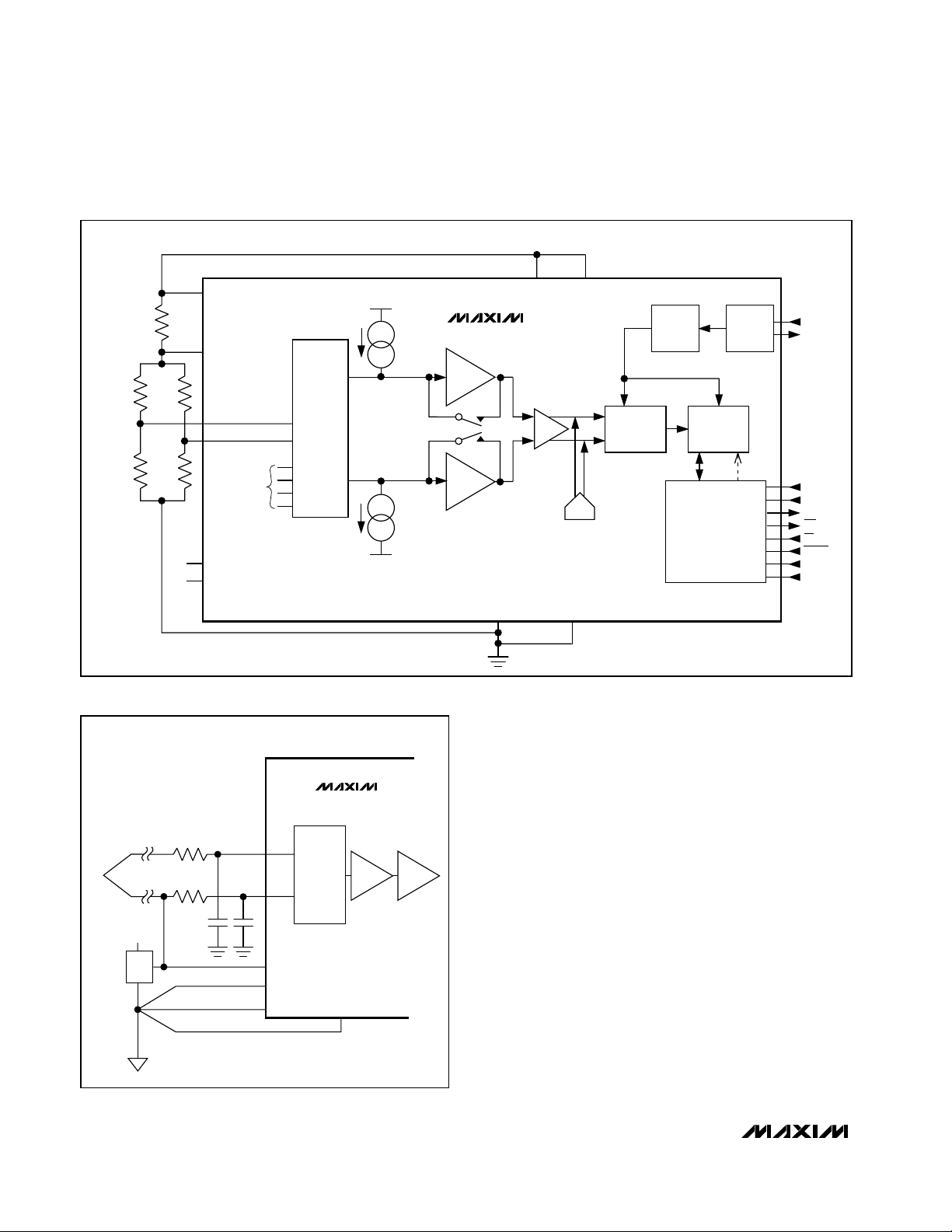
MAX1402
+5V, 18-Bit, Low-Power, Multichannel,
Oversampling (Sigma-Delta) ADC
Strain Gauge Operation
Connect the differential inputs of the MAX1402 to the
bridge network of the strain gauge. In Figure 16, the
analog positive supply voltage powers the bridge network and the MAX1402 along with its reference voltage.
The on-chip PGA allows the MAX1402 to handle an
analog input voltage range as low as 20mV full scale.
The differential inputs of the part allow this analog input
range to have an absolute value anywhere between
AGND and V+.
Temperature Measurement
Figure 17 shows a connection from a thermocouple to
the MAX1402. In this application, the MAX1402 is operated in its buffered mode to allow large decoupling
capacitors on the front end. These decoupling capacitors eliminate any noise pickup form the thermocouple
leads. When the MAX1402 is operated in buffered
mode, it has a reduced common-mode range. In order
to place the differential voltage from the thermocouple
on a suitable common-mode voltage, the AIN2 input of
the MAX1402 is biased at the reference voltage, +2.5V.
BUFFER
BUFFER
DIVIDER
CLOCK
GEN
MODULATOR
DIGITAL
FILTER
V+
V+ V
DD
AGNDOUT1
OUT2
REFIN+
REFIN-
AGND DGND
AIN1
AIN2
SWITCHING
NETWORK
ACTIVE
GAUGE
DUMMY
GAUGE
R
REF
ANALOG SUPPLY
R
R
ADDITIONAL
ANALOG
AND
CALIBRATION
CHANNELS
INTERFACE
AND
CONTROL
SCLK
DIN
DOUT
INT
CS
RESET
DS1
DS0
CLKIN
CLKOUT
PGA
DAC
MAX1402
BUFFER
BUFFER
Figure 16. Strain-Gauge Application with MAX1402
CC
+5V
+2.5V
REFIN+
REFIN-
AGND
DGND
R
R
THERMOCOUPLE
JUNCTION
SWITCHING
NETWORK
PGA
MAX1402
BUFFER
AIN1
AIN2
Figure 17. Thermocouple Application with MAX1402
34 ______________________________________________________________________________________
Page 35

MAX1402
+5V, 18-Bit, Low-Power, Multichannel,
Oversampling (Sigma-Delta) ADC
4–20mA Loop-Powered Transmitters
Low power, single-supply operation, and easy interfacing with optocouplers make the MAX1402 ideal for
loop-powered 4–20mA transmitters. Loop-powered
transmitters draw their power from the 4–20mA loop,
limiting the transmitter circuitry to a current budget of
4mA. Tolerances in the loop further limit this current
budget to 3.5mA. Since the MAX1402 consumes only
250µA, a total of 3.25mA remains to power the remaining transmitter circuitry. Figure 18 shows a block diagram for a loop-powered 4–20mA transmitter.
Power Supplies
No specific power sequence is required for the
MAX1402; either the V+ or the VDDsupply can come
up first. While the latchup performance of the MAX1402
is good, it is important that power be applied to the
MAX1402 before the analog input signals (AIN_) or the
CLKIN inputs, to avoid latchup. If this is not possible,
then the current flow into any of these pins should be
limited to 50mA. If separate supplies are used for the
MAX1402 and the system digital circuitry, then the
MAX1402 should be powered up first.
3-Wire and 4-Wire
RTD Configurations
Tightly matched 200µA current sources compensate for
errors in 3-wire and 4-wire RTD configurations. In the 3wire configuration (Figure 19), the lead resistances
result in errors if only one current source is used. The
200µA will flow through RL1developing a voltage error
between AIN1 and AIN2. An additional current source
compensates for this error by developing an equivalent
voltage across RL2ensuring the differential voltage at
AIN1 and AIN2 is not affected by lead resistance. This
assumes both leads are of the same material and of
equal length (RL1= RL2) and OUT1 and OUT2 have
matching tempcos (5ppm/°C). Both current sources will
flow through RL3developing a common-mode voltage
that will not affect the differential voltage at AIN1 and
AIN2. Using one of the current sources to supply the
reference voltage ensures a more accurate ratiometric
result.
Unlike the 3-wire configuration, the 4-wire configuration
(Figure 20) has no error associated with lead resistances as no current flows in the measurement leads
connected to AIN1 and AIN2. Current source OUT1
provides the excitation current for the RTD and current
source OUT2 provides current to generate the reference voltage. This reference voltage developed across
R
REF
ensures that the analog input voltage span
remains ratiometric to the reference voltage. RTD tempco errors in the analog input voltage are due to the tem-
DAC
R
GAIN
R
OFST
R
X
V
IN+
V
IN-
R
SENSE
4–20mA LOOP
INTERFACE
R
FDBK
R
Y
C
C
ISOLATION
BARRIER
V+
GND
V+
4
SPI
4
SPI
3
SPI
GND
SENSOR
VOLTAGE
REGULATOR
µP/µC
MAX1402
Figure 18. 4–20mA Transmitter
______________________________________________________________________________________ 35
Page 36

MAX1402
+5V, 18-Bit, Low-Power, Multichannel,
Oversampling (Sigma-Delta) ADC
36 ______________________________________________________________________________________
perature drift of the RTD current source and compensated for by the variation in the reference voltage. A
common resistance value for the RTD is 100Ω generat-
ing a 20mV signal directly handled at the analog input
of the MAX1402. The voltage at OUT1 and OUT2 can
go to within 1.0V of the V+ supply.
Grounding and Layout
For best performance, use printed circuit boards with
separate analog and digital ground planes. Wire-wrap
boards are not recommended.
Design the printed circuit board so that the analog and
digital sections are separated and confined to different
areas of the board. Join the digital and analog ground
planes at only one point. If the MAX1402 is the only
device requiring an AGND to DGND connection, then
the ground planes should be connected at the AGND
and DGND pins of the MAX1402. In systems where multiple devices require AGND to DGND connections, the
connection should still be made at only one point. Make
the star ground as close to the MAX1402 as possible.
Avoid running digital lines under the device, because
these may couple noise onto the die. Run the analog
ground plane under the MAX1402 to minimize coupling
of digital noise. Make the power-supply lines to the
MAX1402 as wide as possible to provide low-impedance paths and reduce the effects of glitches on the
power-supply line.
Shield fast switching signals, such as clocks, with digital ground to avoid radiating noise to other sections of
the board. Avoid running clock signals near the analog
inputs. Avoid crossover of digital and analog signals.
Traces on opposite sides of the board should run at
right angles to each other. This will reduce the effects
of feedthrough on the board. A microstrip technique is
best, but is not always possible with double-sided
boards. In this technique, the component side of the
DGND
A = 1 TO 128
PGA
MODULATOR
MAX1402
200µA
200µA
OUT1
AIN1
12.5k
AIN2
OUT2
AGND
R
L3
R
L2
R
L1
V+ V
DD
REFIN-
REFIN+
RTD
Figure 19. 3-Wire RTD Application
Page 37

MAX1402
+5V, 18-Bit, Low-Power, Multichannel,
Oversampling (Sigma-Delta) ADC
______________________________________________________________________________________ 37
Figure 20. 4-Wire RTD Application
V+
200µA
+5V
V
DD
OUT2
REFIN+
AIN1
AIN2
AGND
DGND
PGA
MODULATOR
A = 1 TO 128
200µA
RTD
R
REF
REFIN-
OUT1
MAX1402
board is dedicated to ground planes while signals are
placed on the solder side.
Good decoupling is important when using high-resolution ADCs. Decouple all analog supplies with 10µF tantalum capacitors in parallel with 0.1µF HF ceramic
capacitors to AGND. Place these components as close
to the device as possible to achieve the best decoupling.
See the MAX1402 evaluation kit manual for the recommended layout. The evaluation board package includes
a fully assembled and tested evaluation board.
Optical Isolation
For applications that require an optically isolated
interface, refer to Figure 21. With 6N136-type optocouplers, maximum clock speed is 4MHz. Maximum clock
speed is limited by the degree of mismatch between
the individual optocouplers. Faster optocouplers allow
faster signaling at a higher cost.
2k
2k
6N136
6N136
6N136
6N136
MOSI
470Ω
SCK
MISO
INT
+V
DD
V
CC
V
CC
470Ω
470Ω
470Ω
V
CC
V
CC
INT
ISO
+5V
DOUT
SCLK
DIN
2k
2k
MAX1402
Figure 21. Optically Isolated Interface
Page 38

MAX1402
+5V, 18-Bit, Low-Power, Multichannel,
Oversampling (Sigma-Delta) ADC
38 ______________________________________________________________________________________
SSOP.EPS
Package Information
Chip Information
TRANSISTOR COUNT: 34,648
SUBSTRATE CONNECTED TO AGND
Page 39

MAX1402
+5V, 18-Bit, Low-Power, Multichannel,
Oversampling (Sigma-Delta) ADC
______________________________________________________________________________________ 39
NOTES
Page 40

MAX1402
+5V, 18-Bit, Low-Power, Multichannel,
Oversampling (Sigma-Delta) ADC
Maxim cannot assume responsibility for use of any circuitry other than circuitry entirely embodied in a Maxim product. No circuit patent licenses are
implied. Maxim reserves the right to change the circuitry and specifications without notice at any time.
40
____________________Maxim Integrated Products, 120 San Gabriel Drive, Sunnyvale, CA 94086 408-737-7600
© 1999 Maxim Integrated Products Printed USA is a registered trademark of Maxim Integrated Products.
NOTES
 Loading...