

Page 1
For pricing, delivery, and ordering information, please contact Maxim Direct at 1-888-629-4642,
or visit Maxim’s website at www.maxim-ic.com.
General Description
The MAX1385/MAX1386 set and control bias conditions
for dual RF LDMOS power devices found in cellular
base stations. Each device includes a high-side current-sense amplifier with programmable gains of 2, 10,
and 25 to monitor LDMOS drain current over the 20mA
to 5A range. Two external diode-connected transistors
monitor LDMOS temperatures while an internal temperature sensor measures the local die temperature of the
MAX1385/MAX1386. A 12-bit ADC converts the programmable-gain amplifier (PGA) outputs, external/internal temperature readings, and two auxiliary inputs.
The two gate-drive channels, each consisting of 8-bit
coarse and 10-bit fine DACs and a gate-drive amplifier,
generate a positive gate voltage to bias the LDMOS
devices. The MAX1385 includes a gate-drive amplifier
with a gain of 2 and the MAX1386 gate-drive amplifier
provides a gain of 4. The 8-bit coarse and 10-bit fine
DACs allow up to 18 bits of resolution. The MAX1385/
MAX1386 include autocalibration features to minimize
error over time, temperature, and supply voltage.
The MAX1385/MAX1386 feature an I2C/SPI™-compatible
serial interface. Both devices operate from a 4.75V to
5.25V analog supply (3.2mA supply current), a 2.7V to
5.25V digital supply (3.1mA supply current), and a 4.75V
to 11.0V gate-drive supply (4.5mA supply current). The
MAX1385/MAX1386 are available in a 48-pin thin QFN
package.
Applications
RF LDMOS Bias Control in Cellular Base Stations
Industrial Process Control
Features
♦ Integrated High-Side Drain Current-Sense PGA
with Gain of 2, 10, or 25
♦ ±0.5% Accuracy for Sense Voltage Between 75mV
and 250mV
♦ Full-Scale Sense Voltage of 100mV with Gain of 25
♦ Full-Scale Sense Voltage of 250mV with Gain of 10
♦ Common-Mode Range of 5V to 30V Drain Voltage
for LDMOS
♦ Adjustable Low Noise 0 to 5V, 0 to 10V Output
Gate-Bias Voltage Ranges with ±10mA Gate Drive
♦ Fast Clamp to 0V for LDMOS Protection
♦ 8-Bit DAC Control of Gate-Bias Voltage
♦ 10-Bit DAC Control of Gate-Bias Offset with
Temperature
♦ Internal Die Temperature Measurement
♦ External Temperature Measurement by Diode-
Connected Transistor (2N3904)
♦ Internal 12-Bit ADC Measurement of Temperature,
Current, and Voltages
♦ Selectable I
2
C-/SPI-Compatible Serial Interface
400kHz/1.7MHz/3.4MHz I
2
C-Compatible Control
for Settings and Data Measurement
16MHz SPI-Compatible Control for Settings
and Data Measurement
♦ Internal 2.5V Reference
♦ Three Address Inputs to Control Eight Devices in
I
2
C Mode
MAX1385/MAX1386
Dual RF LDMOS Bias Controllers
with I2C/SPI Interface
________________________________________________________________
Maxim Integrated Products
1
19-4456; Rev 0; 2/09
EVALUATION KIT
AVAILABLE
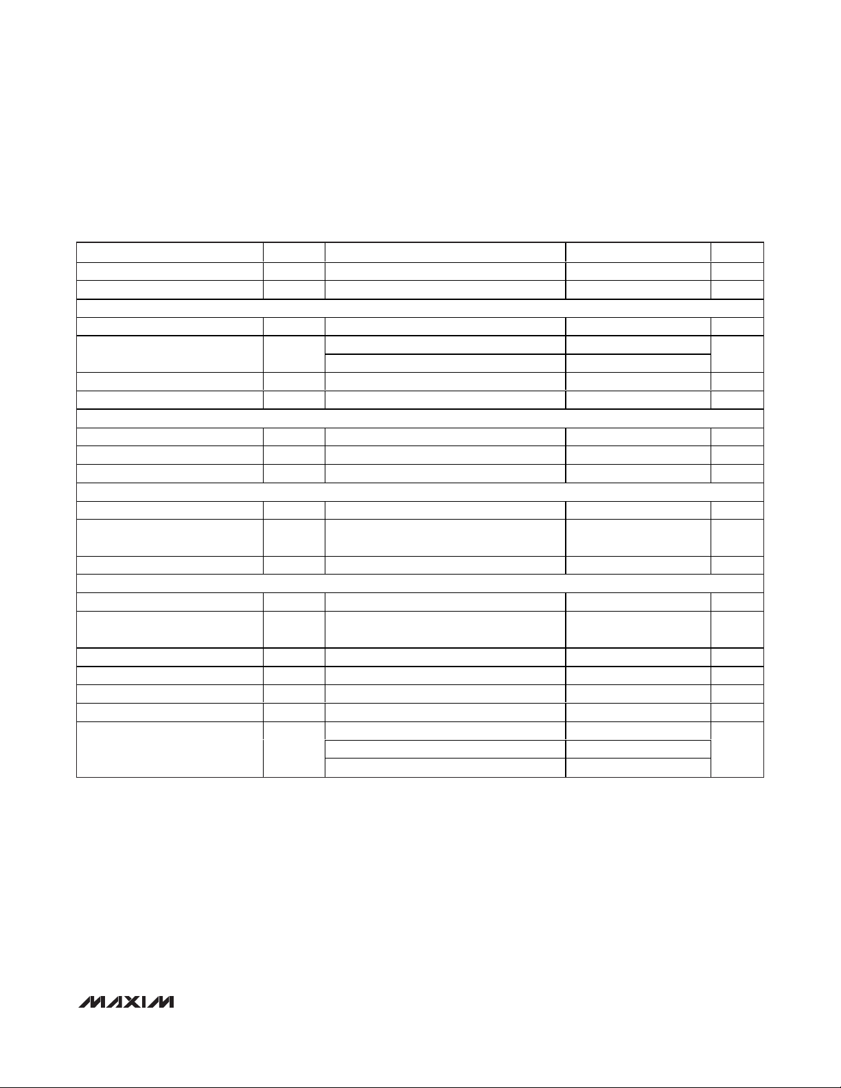
Ordering Information/Selector Guide
SPI is a trademark of Motorola, Inc.
*
EP = Exposed pad.
**
Future product—contact factory for availability.
+
Denotes a lead(Pb)-free/RoHS-compliant package.
Pin Configuration and Typical Operating Circuit (I
2
C Mode)
appear at end of data sheet.
PART TEMP RANGE PIN-PACKAGE TEMP ERROR (°C) V
MAX1385AETM+** -40°C to +85°C 48 Thin QFN-EP* ±1 5
MAX1385BETM+ -40°C to +85°C 48 Thin QFN-EP* ±2 5
MAX1386AETM+** -40°C to +85°C 48 Thin QFN-EP* ±1 10
MAX1386BETM+** -40°C to +85°C 48 Thin QFN-EP* ±2 10
GATE
(V)
Page 2
MAX1385/MAX1386
Dual RF LDMOS Bias Controllers
with I2C/SPI Interface
2 _______________________________________________________________________________________
ABSOLUTE MAXIMUM RATINGS
Stresses beyond those listed under “Absolute Maximum Ratings” may cause permanent damage to the device. These are stress ratings only, and functional
operation of the device at these or any other conditions beyond those indicated in the operational sections of the specifications is not implied. Exposure to
absolute maximum rating conditions for extended periods may affect device reliability.
AVDDto AGND .........................................................-0.3V to +6V
DV
DD
to DGND.........................................................-0.3V to +6V
AGND to DGND.....................................................-0.3V to +0.3V
CS1+, CS1-, CS2+, CS2- to GATEGND.................-0.3V to +32V
CS1- to CS1+, CS2- to CS2+ ...................................-6V to +0.3V
GATEV
DD
to GATEGND .........................................-0.3V to +12V
GATE1, GATE2 to GATEGND...........-0.3V to (GATEV
DD
+ 0.3V)
SAFE1, SAFE2 to GATEGND....................................-0.3V to +6V
GATEGND to AGND..............................................-0.3V to +0.3V
All Other Analog Inputs
to AGND ............-0.3V to the lower of +6V and (AV
DD
+ 0.3V)
Digital Inputs
to DGND ............-0.3V to the lower of +6V and (DV
DD
+ 0.3V)
SDA/DIN, SCL to DGND...........................................-0.3V to +6V
Digital Outputs to DGND .........................-0.3V to (DV
DD
+ 0.3V)
Maximum Continuous Current into Any Pin ........................50mA
Continuous Power Dissipation (T
A
= +70°C)
48-Pin, 7mm x 7mm, Thin QFN (derate 27.8 mW/°C
above +70°C).............................................................2222mW
Maximum Junction Temperature .....................................+150°C
Operating Temperature Range ...........................-40°C to +85°C
Storage Temperature Range .............................-65°C to +150°C
Lead Temperature (soldering, 10s) .................................+300°C
ELECTRICAL CHARACTERISTICS
(GATEVDD= +5.5V for the MAX1385, GATEVDD= +11V for the MAX1386, AVDD= DVDD= +5V, external V
REFADC
= +2.5V, external V
REF-
DAC
= +2.5V, C
REF
= 0.1µF, unless otherwise noted. TA= -40°C to +85°C, unless otherwise noted. Typical values are at TA= +25°C.)
HIGH-SIDE CURRENT SENSE WITH PGA
Common-Mode Input Voltage
Range
Common-Mode Rejection Ratio CMRR 11V < V
Input-Bias Current
Sense Voltage Range for
Accuracy of ±0.5% V
Sense Voltage Range for
Accuracy of ±2% V
Total PGAOUT Voltage Error V
PGAOUT Capacitive Load C
PGAOUT Settling Time t
Saturation Recovery Time
Sense-Amplifier Slew Rate
PARAMETER SYMBOL CONDITIONS MIN TYP MAX UNITS
, V
V
CS+
CS-
V
SENSE
range
PGA gain = 25 0 100
=
PGA gain = 10 0 250Full-Scale Sense Voltage Range
PGA gain = 2 0 1250
PGA gain = 25 75 100
PGA gain = 10 75 250
PGA gain = 2 75 1250
PGA gain = 25 20 100
PGA gain = 10 20 250
PGA gain = 2 20 1250
SENSE
Settles to within ±0.5% of final value, RS =
50Ω, C
Settles to within ±0.5% accuracy; from
V
SENSE
Av
Av
Av
SENSE
SENSE
I
CS+
I
CS-
V
SENSE
VCS_+ -
VCS_-
PGAOUT
HSCS
CS+
< 100mV over the common-mode
= 75mV ±0.1 ±0.5 %
GATE
= 3 x full scale
= 2 0.5
PGA
= 10 2
PGA
= 25 2
PGA
< 30V 90 dB
= 15pF
530V
120 195
0.002 ±2
< 25 µs
< 45 µs
100 pF
µA
mV
mV
mV
V/µs
Page 3
MAX1385/MAX1386
Dual RF LDMOS Bias Controllers
with I2C/SPI Interface
_______________________________________________________________________________________ 3
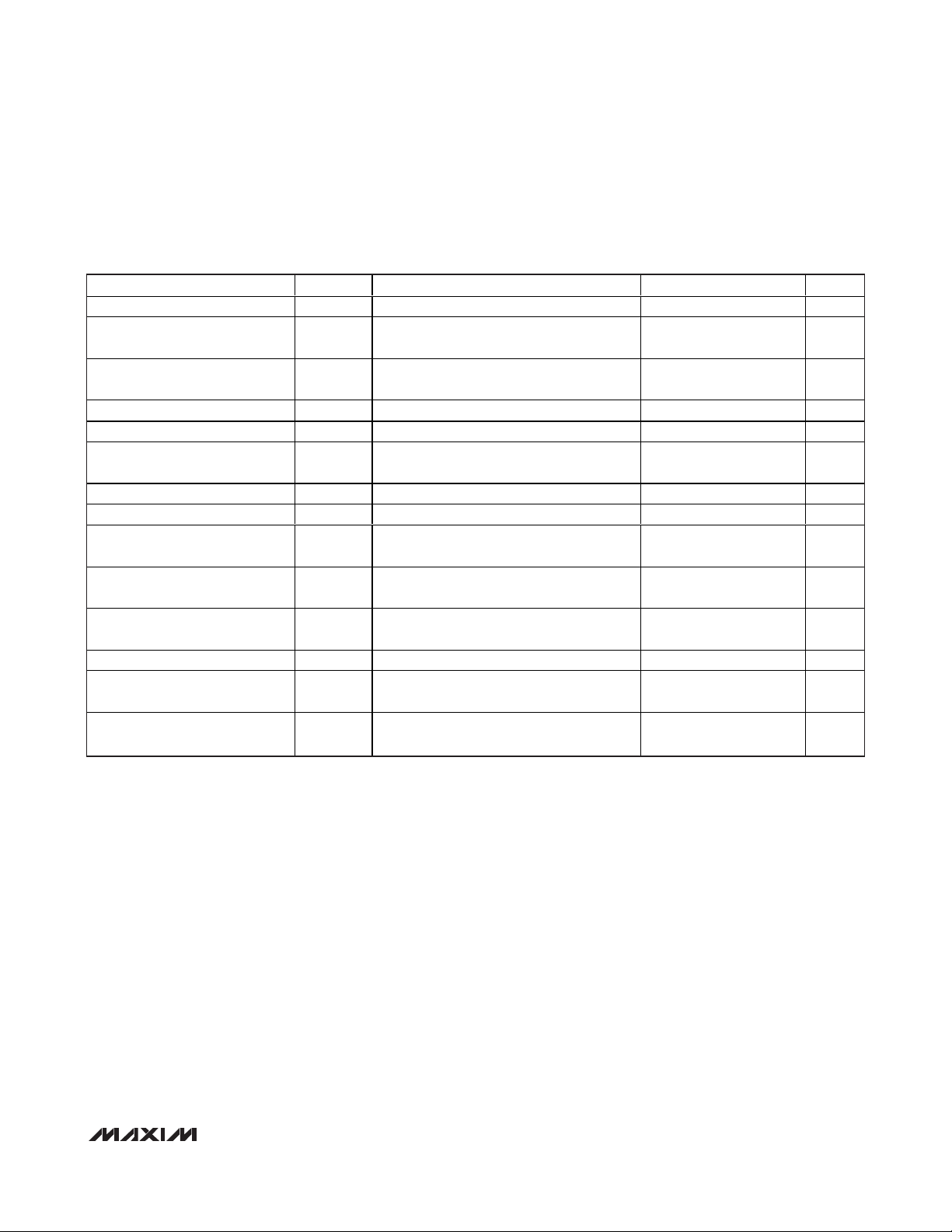
ELECTRICAL CHARACTERISTICS (continued)
(GATEVDD= +5.5V for the MAX1385, GATEVDD= +11V for the MAX1386, AVDD= DVDD= +5V, external V
REFADC
= +2.5V, external V
REF-
DAC
= +2.5V, C
REF
= 0.1µF, unless otherwise noted. TA= -40°C to +85°C, unless otherwise noted. Typical values are at TA= +25°C.)
Sense-Amplifier Bandwidth
LDMOS GATE DRIVER (GAIN = 2 and 4)
Output Gate-Drive Voltage Range V
Output Impedance R
V
Settling Time t
GATE
Output Capacitive Load (Note 1) C
Noise RMS noise; 1kHz - 1MHz 250 nV/√Hz
V
GATE
Maximum Power-On Transient ±100 mV
Output Short-Circuit Current Limit I
Total Unadjusted Error
No Autocalibration and Offset
Removal (Note 2)
Total Adjusted Error
With Autocalibration and Offset
Removal
Drift
Clamp to Zero Delay 1µs
Output Safe Switch OnResistance
Amplifier Bandwidth
Amplifier Slew Rate 0.375 V/µs
MONITOR ADC DC ACCURACY
Resolution N
Differential Nonlinearity DNL
Integral Nonlinearity INL
Offset Error ±2 ±4 LSB
Gain Error (Note 5) ±2 ±4 LSB
Gain Temperature Coefficient ±0.4 ppm/°C
Offset Temperature Coefficient ±0.4 ppm/°C
PARAMETER SYMBOL CONDITIONS MIN TYP MAX UNITS
Av
= 2 900
PGA
Av
= 10 720
PGA
= 25 290
Av
PGA
I
= ±1mA 0.75
GATE
GATE
I
= ±10mA 1
GATE
GATE
GATE
GATE
TUE
TUE
R
OPSW
SC
ADC
Measured at DC 0.1 Ω
Settles to within ±0.5% of final value;
R
= 50Ω, C
SERIES
No series resistance, R
R
= 50Ω 0 25,000
SERIES
1s, sinking or sourcing ±25 mA
MAX1385, LOCODE = 128, HICODE = 180 ±6 ±20
MAX1386, LOCODE = 128, HICODE = 180 ±12 ±40
MAX1385, LOCODE = 128, HICODE = 180 ±1 ±8
MAX1386, LOCODE = 128, HICODE = 180 ±2 ±16
MAX1385, V
MAX1386, V
GATE_ clamped to AGND (Note 3) 500 Ω
MAX1385 300
MAX1386 150
ADC
(Note 4) ±0.6 ±2 LSB
ADC
GATE
GATE
= 15µF
GATE
= 0Ω 010
SERIES
> 1V ±15
> 1V ±30
12 Bits
GATEV
- 0.75
GATEV
- 1
10 ms
±0.5 ±2 LSB
kHz
DD
V
DD
nF
mV
mV
µV/°C
kHz
Page 4
MAX1385/MAX1386
Dual RF LDMOS Bias Controllers
with I2C/SPI Interface
4 _______________________________________________________________________________________
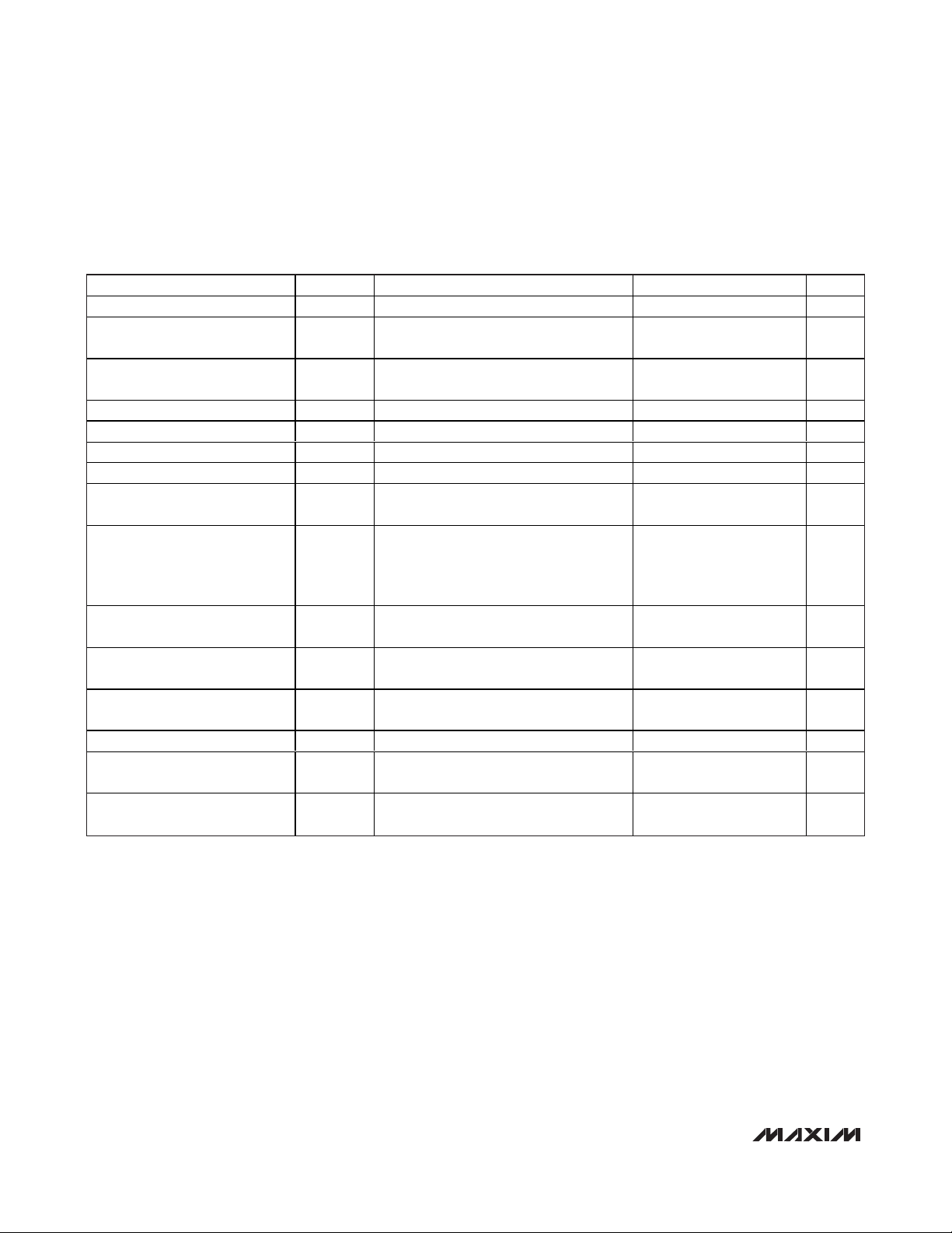
ELECTRICAL CHARACTERISTICS (continued)
(GATEVDD= +5.5V for the MAX1385, GATEVDD= +11V for the MAX1386, AVDD= DVDD= +5V, external V
REFADC
= +2.5V, external V
REF-
DAC
= +2.5V, C
REF
= 0.1µF, unless otherwise noted. TA= -40°C to +85°C, unless otherwise noted. Typical values are at TA= +25°C.)
Channel-to-Channel Offset
Matching
Channel-to-Channel Gain
Matching
MONITOR ADC DYNAMIC ACCURACY (1kHz sine-wave input, 2.5V
Signal-to-Noise Plus Distortion SINAD 70 dB
Total Harmonic Distortion THD Up to the 5th harmonic -82 dB
Spurious-Free Dynamic Range SFDR 86 dB
Intermodulation Distortion IMD f
Full-Power Bandwidth -3dB point 10 MHz
Full-Linear Bandwidth S/(N + D) > 68dB 100 kHz
MONITOR ADC CONVERSION RATE
Power-Up Time t
Conversion Time t
MONITOR ADC ANALOG INPUT (ADCIN1, ADCIN2)
Input Range V
Input Leakage Current VIN = 0V and VIN = AV
Input Capacitance C
TEMPERATURE MEASUREMENTS
Internal Sensor Measurement
Error (Note 1)
External Sensor Measurement
Error (Notes 1, 7)
Temperature Resolution 1/8 °C/LSB
External Diode Drive 2.8 85 µA
Drive Current Ratio (Note 8) 16.5
INTERNAL REFERENCE
REFADC/REFDAC Output Voltage
REFADC/REFDAC Output
Temperature Coefficient
REFADC/REFDAC Output
Impedance
PARAMETER SYMBOL CONDITIONS MIN TYP MAX UNITS
, up to 94.4ksps)
P-P
PU
CONV
ADCIN
ADCIN
V
REFADCTA
V
REFDACTA
TC
REFADC
TC
REFDAC
= 0.99kHz, f
IN1
External reference 0.8
Internal reference 70
Internally clocked 7.5 10 µs
Relative to AGND (Note 6) 0 V
MAX1385A/MAX1386A, TA = +25°C ±0.25
MAX1385A/MAX1386A, TA = T
MAX1385B/MAX1386B, TA = +25°C ±0.25
MAX1385B/MAX1386B, T
TA = +25°C ±0.4
T
= T
A
,
to T
MIN
= +25°C 2.494 2.500 2.506
= +25°C 2.494 2.500 2.506
= 1.02kHz 76 dB
IN2
DD
MAX
A
= T
MIN
MIN
to T
to T
MAX
MAX
-1.0 ±0.25 +1.0
-2.0 ±0.35 +2.0
-3 ±0.75 +3
±0.1 LSB
±0.1 LSB
REF
±0.01 ±1 µA
34 pF
±14 ppm/°C
6.5 kΩ
µs
V
°C
°C
V
Page 5
MAX1385/MAX1386
Dual RF LDMOS Bias Controllers
with I2C/SPI Interface
_______________________________________________________________________________________ 5
ELECTRICAL CHARACTERISTICS (continued)
(GATEVDD= +5.5V for the MAX1385, GATEVDD= +11V for the MAX1386, AVDD= DVDD= +5V, external V
REFADC
= +2.5V, external V
REF-
DAC
= +2.5V, C
REF
= 0.1µF, unless otherwise noted. TA= -40°C to +85°C, unless otherwise noted. Typical values are at TA= +25°C.)
Capacitive Bypass at REF 270 nF
Power-Supply Rejection Ratio PSRR AVDD = +5V ±5% 70 dB
EXTERNAL REFERENCE
REFADC Input Voltage Range V
REFADC Input Current I
REFDAC Input Voltage Range V
REFDAC Input Current Static current when no DAC calibration 0.1 µA
GATE-DRIVER COARSE-DAC DC ACCURACY
Resolution N
Integral Nonlinearity INL
Differential Nonlinearity DNL
GATE-DRIVER FINE-DAC DC ACCURACY
Resolution N
Integral Nonlinearity INL
Differential Nonlinearity DNL
POWER SUPPLIES (Note 10)
Analog Supply Voltage AV
Digital Supply Voltage DV
Gate-Drive Supply Voltage V
Analog Supply Current I
Digital Supply Current I
GATEVDD Supply Current I
PARAMETER SYMBOL CONDITIONS MIN TYP MAX UNITS
REFADC
REFADC
REFDAC
CDAC
CDAC
FDAC
GATEVDD
AVDD
DVDD
GATEVDD
Limited code test 1.0 AV
V
= 2.5V, f
REF
Acquisition/between conversions ±0.01 ±1
(Note 9) 0.5 2.5 V
Measured at GATE; fine DAC set at full scale ±0.15 ±1 LSB
Guaranteed monotonic ±0.05 ±0.5 LSB
CDAC
Measured at GATE; coarse DAC set at full
FDAC
scale
Guaranteed monotonic ±0.1 ±1 LSB
FDAC
DD
DD
AVDD = 5V 3.2 4 mA
DVDD = 2.7V to 5.25V 3.1 4.3 mA
I
AVDD
I
PD
DVDD
I
VDDGATE
= 174ksps 60 80
SAMPLE
8 Bits
10 Bits
4.75 5.25 V
2.7
4.75 11.00 V
3 4.5 7 mA
DD
±0.25 ±4 LSB
AV
DD
+ 0.3
0.1 2
0.1 2Shutdown Current (Note 11) I
0.1 2
V
µA
V
µA
Page 6
MAX1385/MAX1386
Dual RF LDMOS Bias Controllers
with I2C/SPI Interface
6 _______________________________________________________________________________________
ELECTRICAL CHARACTERISTICS (continued)
(GATEVDD= +5.5V for the MAX1385, GATEVDD= +11V for the MAX1386, AVDD= DVDD= +5V, external V
REFADC
= +2.5V, external V
REF-
DAC
= +2.5V, C
REF
= 0.1µF, unless otherwise noted. TA= -40°C to +85°C, unless otherwise noted. Typical values are at TA= +25°C.)
VIH AND VIL FOR SDA/DIN AND SCL IN I2C OPERATION ONLY
Input High Voltage V
Input Low Voltage V
Input Hysteresis V
VIH AND VIL FOR OPSAFE1 AND OPSAFE2
Input High Voltage V
Input Low Voltage V
VIH AND VIL FOR ALL OTHER DIGITAL INPUTS
Input High Voltage V
Input Low Voltage V
VOH AND VOL FOR A1/DOUT (SPI), SDA/DIN, ALARM
Output Low Voltage V
Output High Voltage V
VOH AND VOL FOR SAFE1, SAFE2, BUSY
Output Low Voltage V
Output High Voltage V
PARAMETER SYMBOL CONDITIONS MIN TYP MAX UNITS
IH
IL
HYS
IH
IL
IH
IL
I
OL
OH
OL
OH
= 3mA 0.4 V
SINK
I
SOURCE
I
SINK
I
SOURCE
= 2mA
= 0.5mA 0.4 V
= 0.5mA
0.7 x
DV
DD
0.3 x
DV
DD
0.1 x
DV
DD
2.4 V
0.4 V
2.2 V
0.7 V
DV
DD
- 0.5
DV
DD
- 0.5
V
V
V
V
V
Page 7
MAX1385/MAX1386
Dual RF LDMOS Bias Controllers
with I2C/SPI Interface
_______________________________________________________________________________________ 7
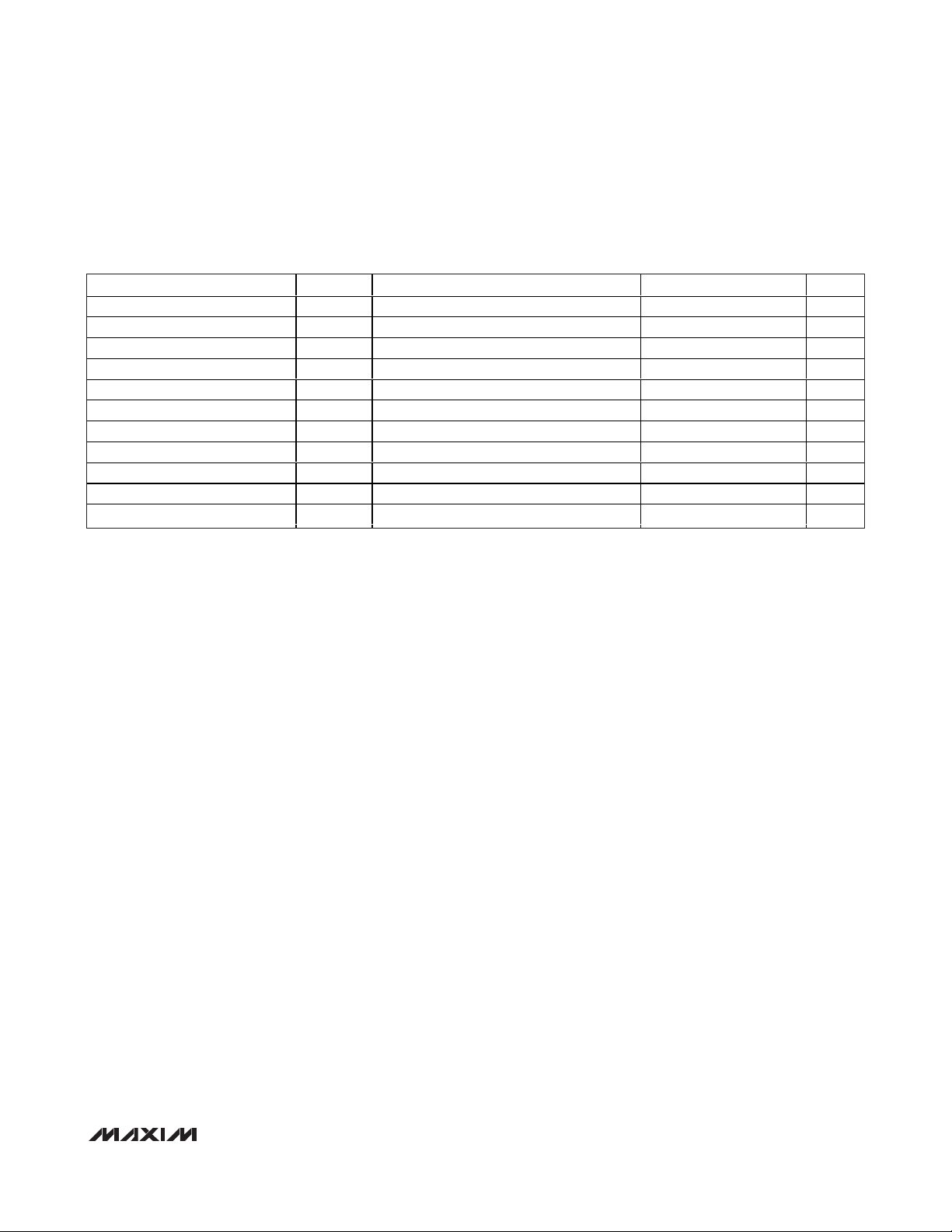
I2C SLOW-/FAST-MODE TIMING CHARACTERISTICS (Note 12, see Figure 1)
(GATEVDD= +5.5V for MAX1385, GATEVDD= +11V for MAX1386, AVDD= +5V, DVDD= 2.7V to 5.25V, external V
REFADC
= +2.5V,
external V
REFDAC
= +2.5V, C
REF
= 0.1µF, TA= -40°C to +85°C, unless otherwise noted).
Serial-Clock Frequency f
Bus Free Time Between STOP
and START Condition
Hold Time Repeated START
Condition
SCL Pulse-Width Low t
SCL Pulse-Width High t
Setup Time Repeated START
Condition
Data Hold Time t
Data Setup Time t
Rise Time of Both SDA and SCL
Signals, Receiving
Fall Time of Both SDA and SCL
Signals, Receiving
Fall Time of SDA Signal,
Transmitting
Setup Time for STOP Condition t
Capacitive Load for Each Bus
Line
Pulse Width of Spikes
Suppressed by the Input Filter
PARAMETER SYMBOL CONDITIONS MIN TYP MAX UNITS
SCL
t
BUF
t
HD;STA
LOW
HIGH
t
SU;STA
HD;DAT
SU;DAT
t
t
t
SU;STO
C
t
SP
After this period, the first clock pulse is
generated
(Note 13) 0 0.9 µs
(Note 14) 0 300 ns
R
(Note 14) 0 300 ns
F
(Notes 14, 15)
F
b
(Note 16) 0 50 ns
0 400 kHz
1.3 µs
0.6 µs
1.3 µs
0.6 µs
0.6 µs
100 ns
20 +
0.1C
b
0.6 µs
250 ns
400 pF
Page 8
MAX1385/MAX1386
Dual RF LDMOS Bias Controllers
with I2C/SPI Interface
8 _______________________________________________________________________________________
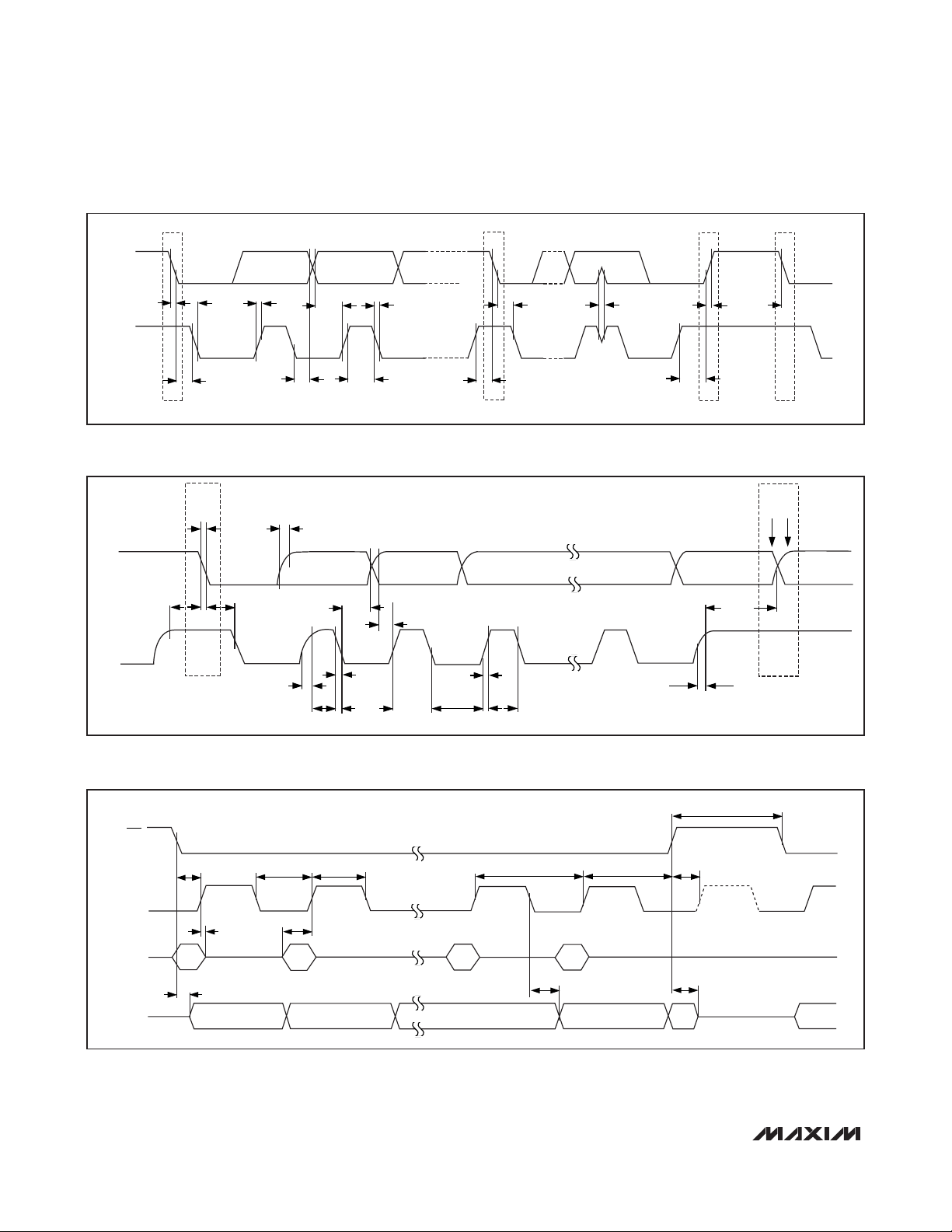
I2C HIGH-SPEED-MODE TIMING CHARACTERISTICS (Note 12, see Figure 2)
(GATEVDD= +5.5V for MAX1385, GATEVDD= +11V for MAX1386, AVDD= +5V, DVDD= 2.7V to 5.25V, external V
REFADC
= +2.5V,
external V
REFDAC
= +2.5V, C
REF
= 0.1µF, TA= -40°C to +85°C, unless otherwise noted).
Serial-Clock Frequency f
Setup Time Repeated START
Condition
Hold Time Repeated START
Condition
SCL Pulse-Width Low t
SCL Pulse-Width High t
Data Setup Time t
Data Hold Time t
Rise Time of SCL Signal,
Receiving
Rise Time of SCL Signal After a
Repeated START Condition and
After an Acknowledge Bit,
Receiving
PARAMETER SYMBOL CONDITIONS MIN TYP MAX UNITS
SCL
t
SU;STA
t
HD;STA
LOW
HIGH
SU;DAT
HD;DAT
t
RCL
t
RCL1
(Note 17) 0 70 ns
0 3.4 MHz
160 ns
160 ns
160 ns
60 ns
10 ns
10 40 ns
10 80 ns
Fall Time of SCL Signal,
Receiving
Rise Time of SDA Signal,
Receiving
Fall Time of SDA Signal,
Transmitting
Setup Time for STOP Condition t
Capacitive Load for Each Bus
Line
Pulse Width of Spikes That are
Suppressed by the Input Filter
t
FCL
t
RDA
t
FDA
SU;STO
C
b
t
SP
10 40 ns
10 80 ns
10 80 ns
160 ns
(Note 18) 100 pF
010ns
Page 9
MAX1385/MAX1386
Dual RF LDMOS Bias Controllers
with I2C/SPI Interface
_______________________________________________________________________________________ 9
Note 1: Guaranteed by design.
Note 2: Total unadjusted errors are for the entire gain drive channel including the 8- and 10-bit DACs and the gate driver. They are
all measured at the GATE1 and GATE2 outputs. Offset removal refers to presetting the drain current after a room temperature calibration by the user. This effectively removes the channel offset.
Note 3: During power-on reset, the output safe switch is closed. The output safe switch opens once both AV
DD
and DVDDsupply
voltages are established.
Note 4: Integral nonlinearity is the deviation of the analog value at any code from its theoretical value after the gain and offset errors
have been removed.
Note 5: Offset nulled.
Note 6: Absolute range for analog inputs is from 0 to AV
DD
.
Note 7: The MAX1385/MAX1386 and external sensor are at the same temperature. External sensor measurement error is tested with
a diode-connected 2N3904.
Note 8: The drive current ratio is defined as the large drive current divided by the small drive current in a temperature measure-
ment. See the
Temperature Measurements
section for further details.
Note 9: Guaranteed monotonicity. Accuracy might be degraded at lower V
REFDAC
.
Note 10: Supply current limits are valid only when digital inputs are at DV
DD
or DGND. Timing specifications are only guaranteed
when inputs are driven rail-to-rail.
Note 11: Shutdown supply currents are typically 0.1µA. Maximum specification is limited by automated test equipment.
Note 12: All timing specifications referred to V
IH
or VILlevels.
Note 13: A master device must provide a hold time of at least 300ns for the SDA signal (referred to V
IL
of SCL) to bridge the unde-
fined region of SCL’s falling edge.
Note 14: C
b
= total capacitance of one bus line in pF; tRand tFare measured between 0.3 x DVDDand 0.7 x DVDD.
Note 15: For a device operating in an I
2
C-compatible system.
Note 16: Input filters on the SDA and SCL inputs suppress noise spikes less than 50ns.
Note 17: A device must provide a data hold time to bridge the undefined part between V
IH
and VILof the falling edge of the SCL signal.
An input circuit with a threshold as low as possible for the falling edge of the SCL signal minimizes this hold time.
Note 18: Cb = total capacitance of one bus line in pF. For bus loads between 100pF and 400pF, the timing parameters should be
linearly interpolated.
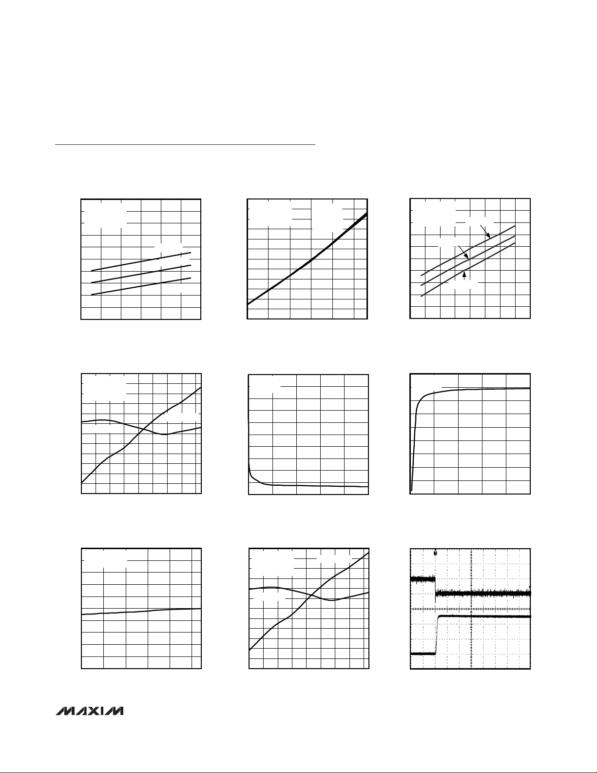
SPI TIMING CHARACTERISTICS (Note 12, See Figure 3)
(GATEVDD= +5.5V for the MAX1385, GATEVDD= +11V for the MAX1386, AVDD= +5V, DVDD= 2.7V to 5.25V, external V
REFADC
=
+2.5V, external V
REFDAC
= +2.5V, C
REF
= 0.1µF, TA= -40°C to +85°C, unless otherwise noted.)
SCL Clock Period t
SCL High Time t
SCL Low Time t
DIN Setup Time t
DIN Hold Time t
SCL Fall to DOUT Transition t
CSB Fall to DOUT Enable t
CSB Rise to DOUT Disable t
CSB Rise or Fall to SCL Rise t
CSB Pulse-Width High t
Last Clock Rise to CSB Rise t
PARAMETER SYMBOL CONDITIONS MIN TYP MAX UNITS
CP
CH
CL
DS
DH
DO
DV
TR
CSS
CSW
CSH
62.5 ns
25 ns
25 ns
10 ns
0ns
C
= 30pF 20 ns
LOAD
C
= 30pF 40 ns
LOAD
C
= 30pF (Note 12) 100 ns
LOAD
25 ns
100 ns
50 ns
Page 10
MAX1385/MAX1386
Dual RF LDMOS Bias Controllers
with I2C/SPI Interface
10 ______________________________________________________________________________________
Figure 1. I2C Slow-/Fast-Mode Timing Diagram
Figure 2. I2C High-Speed-Mode Timing Diagram
Figure 3. SPI Timing Diagram
SDA
t
t
R
t
HD;DAT
SU;DAT
t
HIGH
t
F
t
SU;STA
t
HD;STA
S
r
SCL
t
F
S
t
LOW
t
HD;STA
t
SP
t
SU;STO
t
r
t
BUF
P
S
Sr
t
t
FDA
RDA
SDA
t
SU;STA
t
HD;STA
t
HD;DAT
SCL
t
HIGH
t
FCL
t
LOW
t
RCL1
CSB
SCL
t
CSS
t
DH
t
CL
t
CH
t
DS
t
SU;DAT
t
LOW
t
RCL
t
HIGH
Sr
P
t
SU;STO
t
RCL1
t
CSW
t
t
CP
t
CSH
CSS
DIN
DOUT
D23
t
DV
D22
D1
D0
t
DO
D0D1
t
TR
Page 11
MAX1385/MAX1386
Dual RF LDMOS Bias Controllers
with I2C/SPI Interface
______________________________________________________________________________________ 11
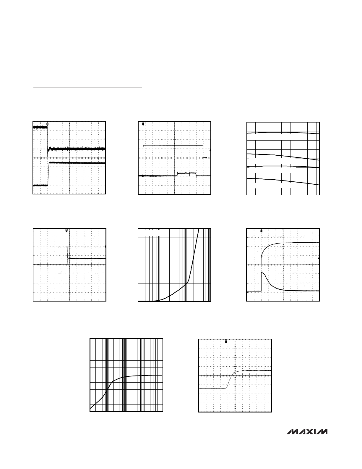
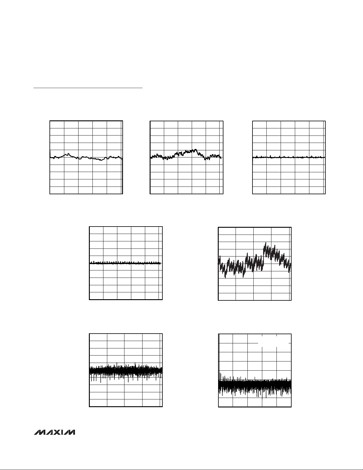
Typical Operating Characteristics
(GATEVDD= +5.5V for the MAX1385, GATEVDD= +11V for the MAX1386, AVDD= DVDD= +5V, external V
REFADC
= +2.5V, external
V
REFDAC
= +2.5V, C
REF
= 0.1µF, TA= +25°C, unless otherwise noted.)
3.0
3.3
3.2
3.1
3.4
3.5
3.6
3.7
3.8
3.9
4.0
4.7 4.94.8 5.0 5.1 5.2 5.3
AVDD SUPPLY CURRENT
vs. AV
DD
VOLTAGE
MAX1385/86 toc01
AVDD (V)
I
AVDD
(mA)
Av
PGA
= 2
CMV = 12V
V
SENSE
= 100mV
TA = +85°C
TA = +25°C
TA = -40°C
DVDD SUPPLY CURRENT vs. DVDD VOLTAGE
MAX1385/86 toc02
DVDD (V)
I
DVDD
(mA)
5.24.74.23.73.2
1.25
1.50
1.75
2.00
2.25
2.50
2.75
3.00
3.25
3.50
3.75
4.00
1.00
2.7
Av
PGA
= 2
CMV = 12V
V
SENSE
= 100mV
TA = +25°C
TA = +85°C
TA = -40°C
GATEVDD SUPPLY CURRENT
vs. GATEV
DD
VOLTAGE
MAX1385/86 toc03
GATEVDD (V)
I
GATEVDD
(mA)
11108 96 75
4.1
4.2
4.3
4.4
4.5
4.6
4.7
4.8
4.9
5.0
4.0
412
Av
PGA
= 2
CMV = 12V
V
SENSE
= 100mV
TA = +85°C
TA = +25°C
TA = -40°C
TOTAL PGAOUT_ ERROR
vs. TEMPERATURE
MAX1385/86 toc04
TEMPERATURE (°C)
PGAOUT_ ERROR (%)
806535 50-10 5 20-25
-0.125
-0.100
-0.075
-0.050
-0.025
0
0.025
0.050
0.075
0.100
0.125
0.150
-0.150
-40
Av
PGA
= 2
CMV = 12V
V
SENSE
= 100mV
ACQUISITION
TRACKING
TOTAL PGAOUT_ ERROR vs. V
SENSE
MAX1385/86 toc05
V
SENSE
(mV)
PGAOUT_ ERROR (%)
1000750500250
0.05
0.10
0.15
0.20
0.25
0.30
0.35
0.40
0.45
0.50
0
0 1250
Av
PGA
= 2
CMV = 12V
TOTAL PGAOUT_ ERROR vs. V
SENSE
MAX1385/86 toc06
V
SENSE
(mV)
PGAOUT_ ERROR (%)
80604020
-3.5
-3.0
-2.5
-2.0
-1.5
-1.0
-0.5
0
0.5
-4.0
0 100
Av
PGA
= 25
CMV = 12V
TOTAL PGAOUT_ ERROR
vs. COMMON-MODE VOLTAGE
MAX1385/86 toc07
COMMON-MODE VOLTAGE (V)
PGAOUT_ ERROR (%)
3025201510
0.01
0.02
0.03
0.04
0.05
0.06
0.07
0.08
0.09
0.10
0
5
Av
PGA
= 2
V
SENSE
= 100mV
PGAOUT_ OFFSET VOLTAGE
vs. TEMPERATURE
MAX1385/86 toc08
TEMPERATURE (°C)
OFFSET VOLTAGE (μV)
806535 50-10 5 20-25
-350
-300
-250
-200
-150
-100
-50
0
50
100
150
200
-400
-40
Av
PGA
= 2
CMV = 12V
V
SENSE
= 100mV
ACQUISITION
TRACKING
V
SENSE
TRANSIENT RESPONSE
MAX1385/86 toc09
100mV/div
1V/div
PGAOUT_
V
SENSE
10μs/div
Page 12
MAX1385/MAX1386
Dual RF LDMOS Bias Controllers
with I2C/SPI Interface
12 ______________________________________________________________________________________
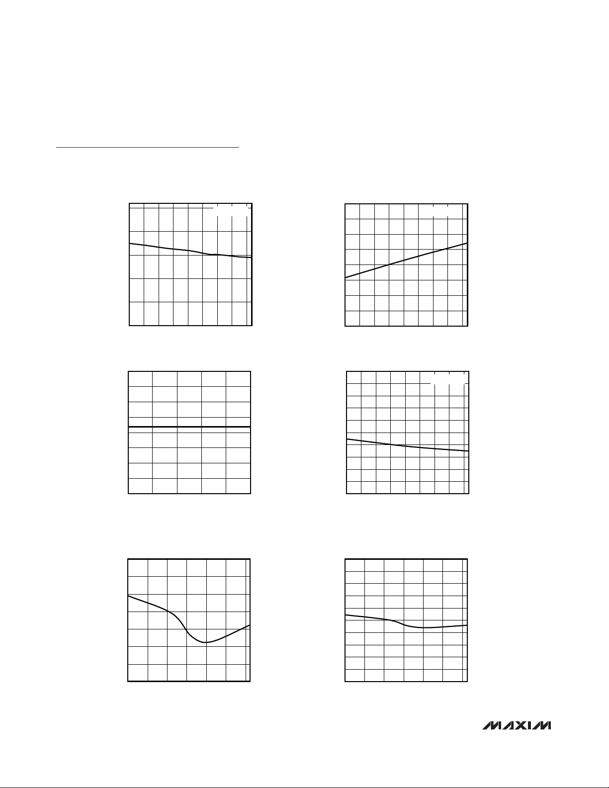
Typical Operating Characteristics (continued)
(GATEVDD= +5.5V for the MAX1385, GATEVDD= +11V for the MAX1386, AVDD= DVDD= +5V, external V
REFADC
= +2.5V, external
V
REFDAC
= +2.5V, C
REF
= 0.1µF, TA= +25°C, unless otherwise noted.)
PGAOUT_ 0mV TO 250mV
V
SENSE
TRANSIENT RESPONSE
MAX1385/86 toc10
V
SENSE
PGAOUT_
10µs/div
100mV/div
1V/div
PGAOUT_ PEDESTAL ERROR
DURING CALIBRATION
MAX1385/86 toc11
BUSY
PGAOUT_
20µs/div
2V/div
10mV/div
GATE_ OFFSET COMPENSATED
ERROR vs. TEMPERATURE
MAX1385/86 toc12
TEMPERATURE (°C)
ERROR VOLTAGE (mV)
8065-25 -10 5 3520 50
-7
-6
-5
-4
-3
-2
-1
0
-8
-40
L_ERROR, AUTOCALIBRATION
H_ERROR, AUTOCALIBRATION
L_ERROR, NO AUTOCALIBRATION
H_ERROR, NO AUTOCALIBRATION
V
GATE
vs. POWER-ON TIME
MAX1385/86 toc13
V
GATE_
400µs/div
50mV/div
CHARGE CURRENT vs. V
GATE
MAX1385/86 toc15
V
GATE_
1ms/div
I
GATE_
2V/div
20mA/div
GATE_ SETTLING TIME
vs. LOAD CAPACITANCE
MAX1385/86 toc14
LOAD CAPACITANCE (µF)
SETTLING TIME (ms)
101
2
4
6
8
10
12
14
16
0
0.1 100
R
SERIES
= 50
Ω
GATE_ VOLTAGE SWING
vs. LOAD RESISTANCE
MAX1385/86 toc16
LOAD RESISTANCE (Ω)
GATE_ VOLTAGE SWING (V)
10,0001000100
1
2
3
4
5
6
7
8
9
10
0
10 100,000
GLITCH ENERGY
MAX1385/86 toc17
1µs/div
10mV/div
Page 13
MAX1385/MAX1386
Dual RF LDMOS Bias Controllers
with I2C/SPI Interface
______________________________________________________________________________________ 13
Typical Operating Characteristics (continued)
(GATEVDD= +5.5V for the MAX1385, GATEVDD= +11V for the MAX1386, AVDD= DVDD= +5V, external V
REFADC
= +2.5V, external
V
REFDAC
= +2.5V, C
REF
= 0.1µF, TA= +25°C, unless otherwise noted.)
-1.0
-0.4
-0.6
-0.8
-0.2
0
0.2
0.4
0.6
0.8
1.0
0 10050 150 200 250
INTEGRAL NONLINEARITY vs. DIGITAL
INPUT CODE (8-BIT COARSE DAC)
MAX1385/86 toc18
DIGITAL INPUT CODE
INL (LSB)
INTEGRAL NONLINEARITY vs. DIGITAL
INPUT CODE (10-BIT FINE DAC)
1.0
0.8
0.6
0.4
0.2
0
INL (LSB)
-0.2
-0.4
-0.6
-0.8
-1.0
0400200 600 800 1000
DIFFERENTIAL NONLINEARITY
vs. DIGITAL INPUT CODE (10-BIT FINE DAC)
1.0
0.8
0.6
0.4
0.2
0
DNL (LSB)
-0.2
-0.4
-0.6
-0.8
-1.0
0 400200 600 800 1000
DIGITAL INPUT CODE
DIGITAL INPUT CODE
MAX1385/86 toc21
DIFFERENTIAL NONLINEARITY
vs. DIGITAL INPUT CODE (8-BIT DAC)
1.0
0.8
MAX1385/86 toc19
0.6
0.4
0.2
0
DNL (LSB)
-0.2
-0.4
-0.6
-0.8
-1.0
0 10050 150 200 250
INTEGRAL NONLINEARITY
vs. DIGITAL OUTPUT CODE (ADC)
1.0
0.8
0.6
0.4
0.2
0
INL (LSB)
-0.2
-0.4
-0.6
-0.8
-1.0
0 20001000 3000 4000
DIGITAL OUTPUT CODE
DIGITAL INPUT CODE
MAX1385/86 toc22
MAX1385/86 toc20
DIFFERENTIAL NONLINEARITY
vs. DIGITAL OUTPUT CODE (ADC)
1.0
0.8
0.6
0.4
0.2
0
DNL (LSB)
-0.2
-0.4
-0.6
-0.8
-1.0
0 20001000 3000 4000
DIGITAL OUTPUT CODE
MAX1385/86 toc23
0
-20
-40
-60
-80
-100
AMPLITUDE (dB)
-120
-140
-160
0 5 10 15 20 25
FFT PLOT
fIN = 303Hz
f
SAMPLE
FREQUENCY (kHz)
= 49.15kHz
MAX1385/86 toc24
Page 14
MAX1385/MAX1386
Dual RF LDMOS Bias Controllers
with I2C/SPI Interface
14 ______________________________________________________________________________________
Typical Operating Characteristics (continued)
(GATEVDD= +5.5V for the MAX1385, GATEVDD= +11V for the MAX1386, AVDD= DVDD= +5V, external V
REFADC
= +2.5V, external
V
REFDAC
= +2.5V, C
REF
= 0.1µF, TA= +25°C, unless otherwise noted.)
2.484
2.489
2.494
2.499
2.504
2.509
-40 -10-25 5 20 35 50 65 80
INTERNAL REFERENCE
vs. TEMPERATURE
MAX1385/86 toc25
TEMPERATURE (°C)
REFERENCE VOLTAGE (V)
AVDD = 5V
-0.100
-0.050
-0.075
0.025
0
-0.025
0.075
0.050
0.100
-40 5 20-25 -10 35 50 65 80
ADC OFFSET ERROR vs. TEMPERATURE
MAX1385/86 toc26
TEMPERATURE (°C)
OFFSET ERROR (%)
AVDD = 5V
ADC OFFSET ERROR vs. AVDD VOLTAGE
0.100
0.075
0.050
0.025
0
-0.025
OFFSET ERROR (%)
-0.050
-0.075
-0.100
4.75 4.85 4.95 5.05 5.15 5.25
AVDD (V)
INTERNAL TEMPERATURE SENSOR
ERROR vs. TEMPERATURE
0
-0.2
-0.4
-0.6
-0.8
ERROR (°C)
-1.0
-1.2
-1.4
-40 0 20-20 40 60 80
TEMPERATURE (°C)
MAX1385/86 toc27
MAX1385/86 toc29
ADC GAIN ERROR vs. TEMPERATURE
0.05
0.04
0.03
0.02
0.01
0
-0.01
GAIN ERROR (%)
-0.02
-0.03
-0.04
-0.05
-40 -10 5 20-25 35 50 65 80
TEMPERATURE (°C)
EXTERNAL TEMPERATURE SENSOR
ERROR vs. TEMPERATURE
1.0
0.8
0.6
0.4
0.2
0
ERROR (°C)
-0.2
-0.4
-0.6
-0.8
-1.0
-40 0 20-20 40 60 80
TEMPERATURE (°C)
AVDD = 5V
MAX1385/86 toc28
MAX1385/86 toc30
Page 15

MAX1385/MAX1386
Dual RF LDMOS Bias Controllers
with I2C/SPI Interface
______________________________________________________________________________________ 15
Pin Description
PIN NAME FUNCTION
1 DGND Digital Ground
2 SAFE1
3 A0/CSB
4 CNVST
5 SEL Mode Select. Connect SEL to DGND to select I2C mode. Connect SEL to DVDD to select SPI mode.
6 ALARM
7 SAFE2
8, 19, 25, 28,
35–39, 42, 46
9 REFDAC DAC Reference Input/Output
10 REFADC ADC Reference Input/Output
11 DXP1
12 DXN1 Diode Negative Input 1. Connect to cathode of temperature diode or the emitter of an npn transistor.
13 DXP2
14 DXN2 Diode Negative Input 2. Connect to cathode of temperature diode or the emitter of an npn transistor.
15 ADCIN1 ADC Input 1
16 ADCIN2 ADC Input 2
17 PGAOUT2 Programmable-Gain Amplifier Output 2
18 AV
20, 21, 22 AGND Analog Ground
N.C. No Connection. Not internally connected.
Safe Status Channel 1 Output. Programmable active-high or active-low. SAFE1 asserts when
programmed channel 1 temperature threshold or current threshold has been reached.
2
I
C-Compatible Address 0/ SPI-Compatible Chip Select. See the Digital Serial Interface section. In
SPI mode, drive A0/CSB low to select the device.
Active-Low Conversion-Start Input. Drive CNVST low to start a conversion (clock modes 01 and 11).
Connect CNVST to DV
Alarm Output. Program ALARM for comparator or interrupt output modes (see the Alarm Modes
section). Program ALARM to assert on any combination of channel temperature or current
thresholds.
Safe Status Channel 2 Output. Programmable active-high or active-low. SAFE2 asserts when
programmed channel 2 temperature threshold or current threshold has been reached.
Diode Positive Input 1. Connect to anode of temperature diode or the base and collector of an npn
transistor.
Diode Positive Input 2. Connect to anode of temperature diode or the base and collector of an npn
transistor.
Analog Power-Supply Input
DD
when initiating conversions through the serial interface (clock mode 00).
DD
Page 16

MAX1385/MAX1386
Dual RF LDMOS Bias Controllers
with I2C/SPI Interface
16 ______________________________________________________________________________________
Pin Description (continued)
PIN NAME FUNCTION
23 GATEGND Gate-Drive Amplifier Ground
24 GATEV
26 OPSAFE2 Operating Safe Channel 2 Input. Drive OPSAFE2 high to clamp GATE2 to AGND.
27 CS2+
29 CS2-
30 GATE2 Channel 2 Gate-Drive Amplifier Output
31 GATE1 Channel 1 Gate-Drive Amplifier Output
32 CS1-
33 CS1+
34 OPSAFE1 Operating Safe Channel 1 Input. Drive OPSAFE1 high to clamp GATE1 to AGND.
40 PGAOUT1 Programmable-Gain Amplifier Output 1
41 A2/N.C.
43 SCL Digital Serial Clock Input
44 SDA/DIN
45 A1/DOUT
47 BUSY Device Busy Output. See the BUSY Output section
48 DV
— EP Exposed Pad. Connect to AGND. Internally connected to analog ground.
DD
Gate-Drive Amplifier Supply Input
DD
Current-Sense Positive Input 2. CS2+ is the external sense resistor connection to the LDMOS 2
supply.
Current-Sense Negative Input 2. CS2- is the external sense resistor connection to the LDMOS 2
drain.
Current-Sense Negative Input 1. CS1- is the external sense resistor connection to the LDMOS 1
drain.
Current-Sense Positive Input 1. CS1+ is the external sense resistor connection to the LDMOS 1
supply.
I2C-Compatible Address 2. See the Digital Serial Interface section.
No Connection. Leave unconnected in SPI mode.
I2C-Compatible Serial Data Input/Output
SPI-Compatible Serial Data Input
I2C-Compatible Address 1. See the Digital Serial Interface section.
SPI-Compatible Serial Data Output
Digital Supply Input
Page 17

MAX1385/MAX1386
Dual RF LDMOS Bias Controllers
with I2C/SPI Interface
______________________________________________________________________________________ 17
Functional Diagram
DV
DGND
SCL
SDA/DIN
A0/CSB
A1/DOUT
A2/N.C.
SAFE2
V
REFDAC
V
REFDAC
ALARM
PGA1
PGA2
DRV
10-BIT DAC
DRV
10-BIT DAC
SAFE1
DIGITAL
CURRENT AND
DD
SERIAL
INTERFACE
TEMPERATURE
COMPARATORS
PGA REGISTERS
REGISTER
SECTION
CHANNEL 1 DAC
REGISTERS
8-BIT HIGH CODE
8-BIT LOW CODE
10-BIT FINE
ADJUST CODE
CHANNEL 1 DAC
REGISTERS
8-BIT HIGH CODE
8-BIT LOW CODE
10-BIT FINE
ADJUST CODE
AV
DD
PGAOUT1
CS1+
CS1-
CS2-
CS2+
PGAOUT2
OPSAFE1
GATE1
GATEV
DD
GATEGND
OPSAFE2
GATE2
AGND
V
REFDAC
MEMORY
REFDAC
FIFO
2.5V
REF
REFADC
V
REFADC
MAX1385
MAX1386
12-BIT ADC
WITH T/H
CONVERSION AND
SCAN OSCILLATOR
AND CONTROL
CNVST
MUX
TEMP
SENSOR
PGAOUT1
PGAOUT2
EXTERNAL
TEMP
PROCESSING
ADCIN0
ADCIN1
DXP1
DXN1
DXP2
DXN2
Page 18

MAX1385/MAX1386
Dual RF LDMOS Bias Controllers
with I2C/SPI Interface
18 ______________________________________________________________________________________
Detailed Description
The MAX1385/MAX1386 set and control bias conditions
for dual RF LDMOS power devices found in cellular
base stations. Each device includes a high-side current-sense amplifier with programmable gains of 2, 10,
and 25 to monitor the LDMOS drain current over the
20mA to 5A range. Two external diode-connected transistors monitor the LDMOS temperatures while an internal temperature sensor measures the local die
temperature of the MAX1385/MAX1386. A 12-bit ADC
converts the programmable-gain amplifier (PGA) outputs, external/internal temperature readings, and two
auxiliary inputs.
The two gate-drive channels, each consisting of 8-bit
coarse and 10-bit fine DACs and a gate-drive amplifier,
generate a positive gate voltage to bias the LDMOS
devices. The MAX1385 includes a gate-drive amplifier
with a gain of 2 and the MAX1386 gate-drive amplifier
provides a gain of 4. The 8-bit coarse and 10-bit fine
DACs allow up to 18 bits of resolution. The MAX1385/
MAX1386 include autocalibration modes to minimize
error over time, temperature, and supply voltage.
The MAX1385/MAX1386 feature an I2C-/SPI-compatible
serial interface. Both devices operate from a 4.75V to
5.25V analog supply (3.2mA supply current), a 2.7V to
5.25V digital supply (3.1mA supply current), and a 4.75V
to 11.0V gate-drive supply (4.5mA supply current).
Power-On Reset
On power-up, the MAX1385/MAX1386 are in full powerdown mode (see the
SSHUT (Write)
section). To change
to normal power mode, write two commands to the
Software Shutdown register. The first command sets
FULLPD to 0 (other bits in the Software Shutdown register
are ignored). A second command is needed to activate
any internal blocks. The recommended sequence of commands to ensure reliable startup following the application
of power, is given in the
Appendix: Recommended
Power-Up Code Sequence
section.
ADC Description
The MAX1385/MAX1386 ADC uses a fully differential
successive approximation register (SAR) conversion
technique and on-chip track-and-hold (T/H) circuitry to
convert temperature and voltage signals into 12-bit digital results. The analog inputs accept single-ended
input signals. Single-ended signals are converted using
a unipolar transfer function. See the ADC transfer function of Figure 25 for more information.
The internal ADC block converts the results of the die
temperature, remote diode temperature readings,
PGAOUT1, PGAOUT2, ADCIN1, or ADCIN2 voltages
according to which bits are set in the ADC Conversion
register (see the
ADCCON (Write)
section). The results
of the conversions are written to FIFO memory. The
FIFO holds up to 15 words (each word is 16 bits) with
channel tags to indicate which channel the 12-bit data
comes from. The FIFO indicates an overflow condition
and an underflow condition (read of an empty FIFO) by
the Flag register (see the
RDFLAG (Read)
section) and
channel tags. The FIFO always stores the most recent
conversion results and allows the oldest data to be
overwritten. Read the latest result stored in the FIFO by
sending the appropriate read command byte (see the
FIFO (Read)
section).
Read the data stored in the FIFO through the FIFO
Read register. The
FIFO (Read)
section details which
channel is being read and whether the FIFO has overflowed.
Analog-to-Digital Conversion Scheduling
The MAX1385/MAX1386 ADC multiplexer scans selected inputs in the order shown in Table 1. The ADC multiplexer skips over the items that are not selected in the
Analog-to-Digital Conversion register. When writing a
conversion command before a conversion is complete,
the pending conversion may be canceled. In addition,
using the serial interface while the ADC is converting
may degrade the performance of the ADC.
ADC Clock Modes
The MAX1385/MAX1386 offer three different conversion/acquisition modes (known as clock modes) selectable through the Device Configuration register (see the
DCFIG (Read/Write)
section). Clock Mode 10 is
reserved and cannot be used. For conversion/acquisition examples and timing diagrams, see the
Applications Information
section.
If the analog-to-digital conversion requires the internal
reference (temperature measurement or voltage measurement with internal reference selected) and the reference has not been previously forced on, the device
inserts a worst-case delay of 81µs, for the reference to
settle, before commencing the analog-to-digital conversion. The reference remains powered up while there are
pending conversions. If the reference is not forced on,
it automatically powers down at the end of a scan or
when CONCONV in the Analog-to-Digital Conversion
register is set back to 0.
Page 19

MAX1385/MAX1386
Dual RF LDMOS Bias Controllers
with I2C/SPI Interface
______________________________________________________________________________________ 19
Clock Mode 00
In clock mode 00, power-up, acquisition, conversion,
and power-down are all initiated by writing to the Analogto-Digital Conversion register and performed automatically using the internal oscillator. This is the default clock
mode. The ADC sets the BUSY output high, powers up,
scans all requested channels, stores the results in the
FIFO, and then powers down. After the scan is complete,
BUSY is pulled low and the results for all the commanded channels are available in the FIFO.
Clock Mode 01
In clock mode 01, power-up, acquisition, conversion,
and power-down are all initiated by setting CNVST low
for at least 40ns. Conversions are performed automatically using the internal oscillator. The ADC sets the
BUSY output high, powers up, scans all requested
channels, stores the results in the FIFO, and then powers down. After the scan is complete, BUSY is pulled
low and the results for all the commanded channels are
available in the FIFO.
Clock Mode 11
In clock mode 11, conversions are initiated one at a
time through CNVST in the order shown in Table 1 and
performed using the internal oscillator. In this mode, the
acquisition time is controlled by the time CNVST is
brought low. CNVST is resynchronized by the internal
oscillator, which means there is a one-clock-cycle
uncertainty (typically 320ns) in the exact sampling
instant. Different timing parameters apply depending
whether the conversion is temperature, voltage, using
the external reference, or using the internal reference.
For a temperature conversion, set CNVST low for at
least 40ns. The BUSY output goes high and the temperature conversion results are available after an additional 94µs (when BUSY goes low again). Thus, the
worst-case conversion time of the initial temperature
sensor scan (allowing the internal reference to settle) is
175µs. Subsequent temperature scans only take 85µs
worst case as the internal reference and temperature
sensor circuits are already powered.
For a voltage conversion while using an internal or
external reference, set CNVST low for at least 2µs but
less than 6.7µs. The BUSY output goes high and the
conversion results are available after an additional
7.5µs (typ) when BUSY goes low again.
Continuous conversion is not supported in this clock
mode (see the
ADCCON (Write)
section).
Changing Clock Modes During ADC Conversions
If a change is made to the clock mode in the Device
Configuration register while the ADC is already performing a conversion (or series of conversions), the following descriptions show how the MAX1385/MAX1386
respond:
• CKSEL = 00 and is then changed to another value
The ADC completes the already triggered series of
conversions and then goes idle. The BUSY output
remains high until the conversions are completed.
The MAX1385/MAX1386 then respond in accordance with the new CKSEL mode.
• CKSEL = 01 and is then changed to another value
If waiting for the initial external trigger, the
MAX1385/MAX1386 immediately exit clock mode
01, power down the ADC, and go idle. The BUSY
output stays low and waits for the external trigger. If
a conversion sequence has started, the ADC completes the requested conversions and then goes
idle. The BUSY output remains high until the conversions are completed. The MAX1385/MAX1386 then
respond in accordance with the new CKSEL mode.
• CKSEL = 11 and is then changed to another value
If waiting for an external trigger, the MAX1385/
MAX1386 immediately exit clock mode 11, power
down the ADC, and go idle. The BUSY output stays
low and waits for the external trigger.
Table 1. Order of ADC Conversion Scan
ORDER OF SCAN DESCRIPTION OF CONVERSION
1 Internal device temperature
2 External diode 1 temperature
3 PGAOUT1 for current sense
4 ADCIN1
5 External diode 2 temperature
6 PGAOUT2 for current sense
7 ADCIN2
Page 20

MAX1385/MAX1386
Dual RF LDMOS Bias Controllers
with I2C/SPI Interface
20 ______________________________________________________________________________________
Figure 4. Equivalent ADC Input Circuit
Analog Input Track and Hold
The equivalent circuit (Figure 4) shows the
MAX1385/MAX1386 ADC input architecture. In track
mode, a positive input capacitor is connected to
ADCIN_ and a negative input capacitor is connected to
AGND. After the T/H enters hold mode, the difference
between the sampled positive and negative input voltages is converted. The input capacitance charging rate
determines the time required for the T/H to acquire an
input signal. If the input signal’s source impedance is
high, the required acquisition time lengthens.
Any source impedance below 300Ω does not significantly affect the ADC’s AC performance. A high-imped-
ance source can be accommodated either by lengthening t
ACQ
or by placing a 1µF capacitor between the
positive input and AGND. The combination of the analog input source impedance and the capacitance at the
analog input creates an RC filter that limits the analoginput bandwidth.
Analog-Input Bandwidth
The ADC’s input-tracking circuitry has a 10MHz bandwidth to digitize high-speed transient events. Anti-alias
prefiltering of the input signals is necessary to avoid
high-frequency signals aliasing into the frequency band
of interest.
ADCIN_
CAPACITIVE DAC
CONTROL LOGIC
AGND
ADCIN_
AGND
TRACK MODE
HOLD/CONVERSION MODE
CAPACITIVE DAC
CONTROL LOGIC
Page 21

MAX1385/MAX1386
Dual RF LDMOS Bias Controllers
with I2C/SPI Interface
______________________________________________________________________________________ 21
Analog-Input Protection
Internal ESD protection diodes clamp all analog inputs
to AVDDand AGND, allowing the inputs to swing from
AGND - 0.3V to AVDD+ 0.3V without damage. If an
analog input voltage exceeds the supplies, limit the
input current to 2mA.
DAC Description
The MAX1385/MAX1386 include two 8-bit and 10-bit
DAC blocks to independently control the voltage on
each LDMOS gate. Both 10-bit and 8-bit DACs can be
automatically calibrated to minimize output error over
time, temperature, and supply voltage. The 8-bit and
10-bit DACs have unipolar transfer functions and have
a relationship to the output voltage by the following
equation:
where LOCODE, HICODE, and FINECODE are the low
wiper (8 bits), high wiper (8 bits), and fine DAC (10 bits)
values written to the DAC by the user. LOCODE,
HICODE, and FINECODE represent the values in the
DAC input registers and may or may not be the actual
values in the DAC output registers depending whether
autocalibration is used or not (see the 8-Bit
Coarse-
DAC Adjustment
section). To find the actual voltage at
GATE_, multiply the V
DACOUT
result by 2 (MAX1385) or
4 (MAX1386). Due to the buffer amplifiers, the voltage
at GATE_ cannot be set below 100mV above AGND. It
is recommended that the LOCODE for DAC1 and DAC2
are set so that the minimum possible output at GATE_
is 200mV (MAX1385) and 400mV (MAX1386).
The DACs can be operated to produce an 18-bit
monotonic DAC with 12-bit (typ) INL. Write to either
HICODE or LOCODE in a leapfrog fashion, without
commanding autocalibration, to configure the 18-bit
monotonic DAC. When LOCODE > HICODE, invert the
value of FINECODE.
8-Bit Coarse-DAC Adjustment
Each DAC control block contains a resistor string with
wipers that serve as an 8-bit coarse DAC. Wipers are
set by writing to the appropriate DAC input registers
and/or using the Load DAC Control register (LDAC)
commands. The output of a coarse DAC is not updated
until the appropriate DAC output register(s) have been
set. See Figure 5 for the relationship between DAC
input registers, DAC output registers, and wipers.
DAC output registers are not directly accessible to the
user. Choose which input register to write to based on
whether automatic low or high calibration is desired, or
if updates to the output of the DAC need to be initiated
immediately. In the case of automatic low or high calibration, a correction code is added to or subtracted
from the 10-bit fine-DAC input register. Transfers from
the DAC input registers to DAC output registers can
occur immediately after a write to the appropriate DAC
input register or on a software command through the
Software LDAC register. See the
Register Descriptions
section for bit-level descriptions of these registers.
10-Bit Fine-DAC Adjustment
Each DAC control block contains a 10-bit fine DAC that
operates between the high and low wiper positions
from the 8-bit coarse DAC. The 10-bit fine DAC also
has an optional automatic calibration mode and can be
updated immediately or on a software-issued command
in the Software LDAC register. Writing to the appropriate fine-DAC input register determines whether automatic calibration is used and/or when the DAC is
updated. See Figure 6 for the relationship between
DAC input registers, DAC output registers, and the
Software LDAC register.
The fine-DAC output registers are not directly accessible. Choose which DAC input register to write to based
on whether automatic fine calibration is desired, or
whether updates to the output of the DAC need to be initiated immediately. In the case of automatic fine calibration, a correction code is added to or subtracted from
the input register code and transferred to the appropriate
fine-DAC output register. Transfers from a fine-DAC input
register to a fine-DAC output register can occur immediately after a write to the appropriate DAC input register or
on a software command through the Software LDAC register. See the
Register Descriptions
section for bit-level
detail of these registers.
V
DACOUT
V
REF REF
LOCODE
=× +× − ×
88 10
22 2
V
HICODE LOCODE
[]
FINECODE
Page 22

MAX1385/MAX1386
Dual RF LDMOS Bias Controllers
with I2C/SPI Interface
22 ______________________________________________________________________________________
Figure 6. Fine-DAC Register Diagram
Figure 5. Coarse-DAC Register Diagram
HIGH-CAL
COARSE DAC_ HIGH WIPER OUTPUT REGISTER
HIWIPE_ REGISTER
THRUHI_ REGISTER
THRULO_ REGISTER
INPUT REGISTERS
HCAL
V
DACREF
TO 10-BIT FINE DAC
LOWIPE_ REGISTER
LCAL
LOW-CAL
FROM 8-BIT COARSE DAC
LOAD DAC CONTROL REGISTER (LDAC)
FINE_ REGISTER
FINECAL_ REGISTER
COARSE DAC_ LOW WIPER OUTPUT REGISTER
LOAD DAC CONTROL REGISTER (LDAC)
FINE DAC_ OUTPUT REGISTER
10-BIT FINE
DAC
TO GATE-DRIVE BLOCK
FINECALTHRU_ REGISTER
INPUT REGISTERS
FINETHRU_ REGISTER
FROM 8-BIT COARSE DAC
FINE-CAL
Page 23

MAX1385/MAX1386
Dual RF LDMOS Bias Controllers
with I2C/SPI Interface
______________________________________________________________________________________ 23
ADC/DAC References
The MAX1385/MAX1386 provide an internal low-noise
2.5V reference for the ADCs, DACs, and temperature
sensor. See the
Device Configuration Register
section
for information on configuring the device for external or
internal reference. Connect a voltage source to
REFADC in the 1V to AVDDrange when using an external ADC reference. Connect a voltage source to REFDAC in the 0.5V to 2.5V range when using an external
DAC reference. When using an external voltage reference, bypass the reference pin with a 0.1µF capacitor
to AGND.
The internal reference has a lowpass filter to reduce
noise. The device allows 60µs (typ) and 81µs (typ) worst
case for the reference to settle before permitting an analog-to-digital conversion. If reference mode 11 is selected, the required settling time is longer. In this case, the
user should set at least one of DAC1PD, DAC2PD, or
FBGON in the Software Shutdown register, any of which
forces the reference to be permanently powered up.
Temperature Measurements
The MAX1385/MAX1386 measure the internal die temperature and two external remote-diode temperature
sensors. Set up a temperature conversion by writing
to the Analog-to-Digital Conversion register (see the
ADCCON (Write)
section). Optionally program SAFE1
and SAFE2 outputs to depend on programmed temperature thresholds.
The MAX1385/MAX1386 can perform temperature measurements with an internal diode-connected transistor.
The diode bias current changes from 66µA to 4µA to
produce a temperature-dependent bias voltage difference. The second conversion result at 4µA is subtracted from the first at 66µA to calculate a digital value that
is proportional to the absolute temperature. The stored
data result is the aforementioned digital code minus an
offset to adjust from Kelvin to Celsius.
The reference voltage for the temperature measurements is always derived from the internal reference
source. Temperature results are in degrees Celsius
(two’s-complement form).
The temperature-sensing circuits power up for the first
temperature measurement in an analog-to-digital conversion scan. The temperature-sensing circuits remain
powered until the end of the scan to avoid a possible
67µs delay of internal reference power-up time for each
individual temperature channel. If the continuous convert bit CONCONV is set high and the current ADC
channel selection includes a temperature channel, the
temperature-sensor circuits remain powered up until
the CONCONV bit is set low.
The external temperature-sensor drive current ratio has
been optimized for a 2N3904 npn transistor with an ideality factor of 1.0065. The nonideality offset is removed
internally by a preset digital coefficient. Use of a transistor with a different ideality factor produces a proportionate difference in the absolute measured
temperature. More details on this topic and others related to using an external temperature sensor can be
found in Maxim Application Note 1057:
Compensating
for Ideality and Series Resistance Differences Between
Thermal Sense Diodes
and Application Note 1944:
Temperature Monitoring Using the MAX1253/MAX1254
and MAX1153/MAX1154
.
High-Side Current-Sense PGAs
The MAX1385/MAX1386 provide two high-side currentsense amplifiers with programmable gain. The currentsense amplifiers are unidirectional and provide a 5V to
30V input common-mode range. Both CS1+ and CS2+
must be within the specified common-mode range for
proper operation of each amplifier.
The sense amplifiers measure the load current, I
LOAD
,
through an external sense resistor, R
SENSE_
, between
the CS_+ and CS_- inputs. The full-scale sense voltage
range (V
SENSE_
= V
CS_
+ - V
CS_
-) depends on the pro-
grammed gain, Av
PGA_
(see the
DCFIG (Read/Write)
section). The sense amplifiers provide a voltage output
at PGAOUT_ according to the following equation:
These outputs are also routed to the internal 12-bit ADC
so that a digital representation of the amplified voltages
can be read through the FIFO.
The PGA scales the sensed voltages to fit the input
range of the ADC. Program the PGA with gains of 2, 10,
and 25 by setting the PGSET_ bits (see the
DCFIG
(Read/Write)
section). The input stages have nominal
input offset voltages of 0mV that can be adjusted by a
trim DAC (not shown in the
Functional Diagram
) over the
-3mV to +3mV range in 25µV steps. Autocalibration can
be used to control the trim DAC to minimize the effective
channel input offset voltage (see the
PGACAL (Write)
section). The PGA feedback network is referenced to
AGND.
ALARM Output
The state of ALARM is logically equivalent to the inclusive OR of SAFE1 and SAFE2. The exception to this
statement is when ALARM is configured for output interrupt mode (see the
Alarm Modes
section). When in output-interrupt mode, ALARM stays in its asserted state
until its associated flag is cleared by reading from the
VAvVV
PGAOUT PGA CS CS____
()=×+−−
Page 24

MAX1385/MAX1386
Dual RF LDMOS Bias Controllers
with I2C/SPI Interface
24 ______________________________________________________________________________________
Figure 7. Window-Threshold-Mode Diagram
Flag register. Configure ALARM for open-drain/pushpull and active-high/active-low by setting the respective
bits in the Hardware Alarm Configuration register.
SAFE1/SAFE2 Outputs
Set up the SAFE1 and SAFE2 outputs to allow WiredOR/AND-type logic functions or to create additional
interrupt-type signals to replace or supplement the
existing ALARM output. SAFE1 and SAFE2 do not have
any internal pullup/pulldown devices.
The SAFE1 and SAFE2 output buffers are CMOS-compatible, noninverting, output buffers capable of driving
to within 0.5V of either digital rail. The SAFE1 and
SAFE2 outputs power up as active-high CMOS outputs
with standard logic levels. Configure the SAFE1 and
SAFE2 outputs for open-drain or push-pull by setting
the appropriate bits in the Hardware Alarm
Configuration register. When configuring SAFE1 and
SAFE2 as open-drain outputs, an external pullup resistor is required.
BUSY Output
The BUSY output is forced high to show that the
MAX1385/MAX1386 are busy for a variety of reasons:
• The ADC is in the middle of a user-commanded con-
version cycle (but not in continuous convert mode)
• The ADC is in the middle of an internally triggered
conversion cycle (for a self-calibration measurement)
• The device is in the middle of DAC calibra-
tion calculations
• The device is in the middle of power-up initialization
• One of the PGA channels is undergoing self-calibration
The serial interface remains active regardless of the
state of the BUSY output. Wait until BUSY goes low to
read the current conversion data from the FIFO. When
BUSY is high as a result of an ADC conversion, do not
enter a second conversion command until BUSY has
gone low to indicate the previous conversion is complete. The rising edge of BUSY occurs on the next internal oscillator clock after the start of a new conversion
(either by CNVST or an interface command).
HIGHEST POSSIBLE THRESHOLD
VALUE (DEFAULT VALUE FOR HIGH
THRESHOLD REGISTER)
ALARM OUTPUT ASSERTED
WHEN MEASURED VALUE
RISES ABOVE THIS LEVEL
BUILT-IN 8 TO 64 LSBs
OF HYSTERESIS
RANGE OF VALUES THAT DO NOT CAUSE AN ALARM
BUILT-IN 8 TO 64 LSBs
OF HYSTERESIS
ALARM OUTPUT ASSERTED
WHEN MEASURED VALUE
FALLS BELOW THIS LEVEL
*ONLY WHEN ALARM IS CONFIGURED FOR OUTPUT-COMARATOR MODE.
WHEN IN OUTPUT-INTERRUPT MODE, FLAG REGISTER MUST BE READ
FOR ALARM TO BE DEASSERTED.
ALARM OUTPUT DEASSERTED
WHEN MEASURED VALUE FALLS
BELOW THIS LEVEL*
HIGH THRESHOLD
LOW THRESHOLD
ALARM OUTPUT DEASSERTED
WHEN MEASURED VALUE RISES
ABOVE THIS LEVEL*
LOWEST POSSIBLE THRESHOLD
VALUE (DEFAULT VALUE FOR HIGH
THRESHOLD REGISTER)
Page 25

MAX1385/MAX1386
Dual RF LDMOS Bias Controllers
with I2C/SPI Interface
______________________________________________________________________________________ 25
In single-conversion mode (CKSEL = 11), the BUSY
signal remains high until the ADC has completed the
current conversion (not the entire scan, just the current
conversion), the data has been moved into the FIFO,
and the alarm limits for the channel have been checked
(if enabled). In multiple-conversion mode (CKSEL = 01
or CKSEL = 00), the BUSY signal remains high until all
channels have been scanned and the data from the
final channel has been moved into the FIFO and
checked for alarm limits (if enabled). In continuous-conversion mode (CONCONV = 1), the BUSY signal does
not go high as a result of ADC conversions; however,
BUSY does go high when CONCONV is removed and
remains high until the current scan is complete and the
ADC sequence halts.
After commanding any of the DAC autocalibration components, wait for BUSY to go low before setting OSCPD to 1.
Alarm Modes
The MAX1385/MAX1386 contain several programmable
modes for configuring outputs ALARM, SAFE1, and
SAFE2 behavior. Window-threshold mode allows SAFE_
to assert when the temperature/current is too high or
too low (outside the window). Hysteresis-threshold
mode allows SAFE_ to assert when the temperature/
current is too high, and then to deassert when the temperature/current falls back to an appropriate level.
ALARM asserts when SAFE1 and/or SAFE2 asserts.
Program ALARM for output-comparator mode to stay
asserted after an alarm condition until temperature/current levels are back below programmed thresholds.
Program ALARM for output-interrupt mode to stay
asserted after an alarm condition until the Flag register
is read.
Window-Threshold Mode
In window-threshold mode, ADC readings of
current/temperature are compared to the configured
current/temperature low/high thresholds that are programmed to cause an alarm condition. If an ADC reading falls out of the configured window and ALARM is
configured for output-comparator mode, ALARM
asserts until the current/temperature reading falls back
into the window (past the built-in hysteresis). If an ADC
reading falls out of the configured window and ALARM
is configured for output-interrupt mode, ALARM asserts
until the Flag register is read. Set the amount of built-in
hysteresis from 8 LSBs to 64 LSBs (see the
ALMSCFG
(Read/Write)
section). See Figures 7 and 8.
Figure 8. Window-Threshold-Mode Timing Diagram
MEASUREMENT VALUE
(TEMPERATURE OR CURRENT)
HIGH THRESHOLD
BUILT-IN HYSTERESIS
BUILT-IN HYSTERESIS
LOW THRESHOLD
ALARM OUTPUT
COMPARATOR MODE
OUTPUT-
(ACTIVE LOW)
OUTPUT-
INTERRUPT MODE
(ACTIVE LOW)
FLAG REGISTER
READ
FLAG REGISTER
READ
FLAG REGISTER
READ
TIME
TIME
Page 26

MAX1385/MAX1386
Dual RF LDMOS Bias Controllers
with I2C/SPI Interface
26 ______________________________________________________________________________________
Hysteresis-Threshold Mode
In hysteresis-threshold mode, ADC readings of
current/temperature are compared to the configured
current/temperature low/high thresholds that are programmed to cause an alarm condition. If an ADC reading exceeds its respective configured threshold and
ALARM is configured for output-comparator mode,
ALARM asserts until the current/temperature reading
falls back below its respective threshold. If an ADC
reading exceeds its respective configured threshold
and ALARM is configured for output-interrupt mode,
ALARM asserts until the Flag register is read. See
Figures 9 and 10.
Register Descriptions
Communicate with the MAX1385/MAX1386 through the
I2C/SPI-compatible serial interface. Complete read and
write operations consist of slave address bytes, command bytes, and data bytes. The following register
descriptions cover the contents of command bytes and
data bytes. See the
Digital Serial Interface
section for a
detailed description of how to construct full read and
write operations. All registers are volatile and are reset
to default states upon removal of power. These default
states are referred to as power-on reset (POR) states.
All accessible MAX1385/MAX1386 registers are shown
in Table 2.
TH1 and TH2 (Read/Write)
Write to Channel 1 and Channel 2 High Temperature
Threshold registers by sending the appropriate write
command byte followed by data bits D15–D0 (see Table
3). Bits D15–D12 are don’t care. Read channel 1 and
channel 2 high-temperature thresholds by sending the
appropriate read command byte. Channel 1 and
Channel 2 Temperature Threshold registers are compared to temperature readings from the remote diode
connected transistors. Temperature data is in two’s-complement format and the LSB corresponds to 1/8°C (see
Figure 26 for the Temperature Transfer Function).
TL1 and TL2 (Read/Write)
Write to Channel 1 and Channel 2 Low-TemperatureThreshold registers by sending the appropriate write
command byte followed by data bits D15–D0 (see Table
4). Bits D15–D12 are don’t care. Read channel 1 and
channel 2 low-temperature thresholds by sending the
appropriate read command. Channel 1 and Channel 2
Temperature Threshold registers are compared to temperature readings from the remote diode connected transistors. Temperature data is in two’s-complement format
and the LSB corresponds to 1/8°C (see Figure 26 for the
Temperature Transfer Function).
Figure 9. Hysteresis-Threshold-Mode Diagram
ALARM OUTPUT ASSERTED
WHEN MEASURED VALUE
RISES ABOVE THIS LEVEL
ALARM OUTPUT ASSERTED
WHEN MEASURED VALUE
FALLS BELOW THIS LEVEL
RANGE OF VALUES THAT DO NOT CAUSE AN ALARM
*ONLY WHEN ALARM IS CONFIGURED FOR OUTPUT-COMARATOR MODE.
WHEN IN OUTPUT-INTERRUPT MODE, FLAG REGISTER MUST BE READ
FOR ALARM TO BE DEASSERTED.
HIGHEST POSSIBLE THRESHOLD
VALUE (DEFAULT VALUE FOR HIGH
THRESHOLD REGISTER)
HIGH THRESHOLD
LOW THRESHOLD
LOWEST POSSIBLE THRESHOLD
VALUE (DEFAULT VALUE FOR LOW
THRESHOLD REGISTER)
Page 27

MAX1385/MAX1386
Dual RF LDMOS Bias Controllers
with I2C/SPI Interface
______________________________________________________________________________________ 27
Table 2. Register Listing (See
Appendix: Recommended Power-Up Code Sequence
section)
REGISTER DESCRIPTION MNEMONIC
Analog-to-Digital Conversion ADCCON 62 —
Channel 1 High-Current Threshold IH1 24 A4
Channel 1 High-Temperature Threshold TH1 20 A0
Channel 1 Low-Current Threshold IL1 26 A6
Channel 1 Low-Temperature Threshold TL1 22 A2
Channel 2 High-Current Threshold IH2 2C AC
Channel 2 High-Temperature Threshold TH2 28 A8
Channel 2 Low-Current Threshold IL2 2E AE
Channel 2 Low-Temperature Threshold TL2 2A AA
Coarse DAC1 High Wiper Input HIWIPE1 34 B4
Coarse DAC1 Low Wiper Input LOWIPE1 36 B6
Coarse DAC1 Write-Through High Wiper Input THRUHI1 74 B4
Coarse DAC1 Write-Through Low Wiper Input THRULO1 76 B6
Coarse DAC2 High Wiper Input HIWIPE2 3A BA
Coarse DAC2 Low Wiper Input LOWIPE2 3C BC
Coarse DAC2 Write-Through High Wiper Input THRUHI2 7A BA
Coarse DAC2 Write-Through Low Wiper Input THRULO2 7C BC
Device Configuration DCFIG 30 B0
FIFO Memory FIFO — 80
Fine DAC1 Input Read RDFINE1 — B8
Fine DAC1 Input Register with Autocalibration FINECAL1 38 —
Fine DAC1 Input Without Autocalibration FINE1 50 —
Fine DAC1 Write-Through Input with Autocalibration FINECALTHRU1 78 —
Fine DAC1 Write-Through Input Without Autocalibration FINETHRU1 52 —
Fine DAC2 Input Read RDFINE2 — BE
Fine DAC2 Input Register with Autocalibration FINECAL2 3E —
Fine DAC2 Input Without Autocalibration FINE2 54 —
Fine DAC2 Write-Through Input with Autocalibration FINECALTHRU2 7E —
Fine DAC2 Write-Through Input Without Autocalibration FINETHRU2 56 —
Flag RDFLAG — EA
Hardware Alarm Configuration ALMHCFG 60 E0
PGA Calibration Control PGACAL 4E —
Software Clear SCLR 68 —
Software LDAC LDAC 66 —
Software Shutdown SSHUT 64 —
Software Alarm Configuration ALMSCFG 32 B2
HEX COMMAND
WRITE READ
Page 28

MAX1385/MAX1386
Dual RF LDMOS Bias Controllers
with I2C/SPI Interface
28 ______________________________________________________________________________________
IH1 and IH2 (Read/Write)
Write to Channel 1 and Channel 2 High-CurrentThreshold registers by sending the appropriate write
command byte followed by data bits D15–D0 (see
Table 5). Bits D15–D12 are don’t care. Read channel 1
and channel 2 high-current thresholds by sending the
appropriate read command byte. Channel 1 and
Channel 2 Current-Threshold registers are compared to
ADC readings at PGAOUT1 and PGAOUT2. Use the
following equation to find the required threshold code
for a specified threshold current:
where I
DRAIN
is the current threshold in amperes,
R
SENSE
is the sense resistor, Av
PGA
is the voltage gain
of the PGA, V
REFADC
is the ADC reference voltage, and
I
THRESH
is the resulting threshold register value
in decimal.
IL1 and IL2 (Read/Write)
Write to Channel 1 and Channel 2 Low-CurrentThreshold registers by sending the appropriate write
command byte followed by data bits D15–D0 (see
Table 6). Bits D15–D12 are don’t care. Read channel 1
and channel 2 low-current thresholds by sending the
appropriate read command byte. Channel 1 and
Channel 2 Low-Current Threshold registers are compared to ADC readings at PGAOUT1 and PGAOUT2.
Figure 10. Hysteresis-Threshold-Mode Timing Diagram
Table 3. TH1 and TH2 (Read/Write)
X = Don’t care.
MEASUREMENT VALUE
(TEMPERATURE OR CURRENT)
HIGH THRESHOLD
LOW THRESHOLD
ALARM OUTPUT
COMPARATOR MODE
OUTPUT-
(ACTIVE LOW)
OUTPUT-
INTERRUPT MODE
(ACTIVE LOW)
FLAG REGISTER
READ
FLAG REGISTER
READ
D15 D14 D13 D12
POR XXXX0 111111111 1 1
Bit Value
(°C)
X X X X -256 +128 +64 +32 +16 +8 +4 +2 +1 +0.5 +0.25 +0.125
D11
(MSB)
IIRAv
THRESH DRAIN SENSE PGA
=× × ×
D10 D9 D8 D7 D6 D5 D4 D3 D2 D1
4096
V
REFADC
TIME
TIME
D0
(LSB)
Page 29

MAX1385/MAX1386
Dual RF LDMOS Bias Controllers
with I2C/SPI Interface
______________________________________________________________________________________ 29
Use the following equation to find the required threshold code for a specified threshold current:
where I
DRAIN
is the current threshold in amperes,
R
SENSE
is the sense resistor, Av
PGA
is the voltage gain
of the PGA, V
REFADC
is the ADC reference voltage, and
I
THRESH
is the resulting threshold register value
in decimal.
DCFIG (Read/Write)
Select PGA gain settings, clock modes, and DAC and
ADC reference modes by sending the appropriate write
command byte followed by data bits D15–D0 (see
Table 7). Bits D15–D10 are don’t care. Read the Device
Configuration register by sending the appropriate read
command byte. Program PG2SET1 and PG2SET0 to set
channel 2’s current-sense amplifier gain (see Table 7a).
Program PG1SET1 and PG1SET0 to set channel 1’s
current-sense amplifier gain (see Table 7a). Set
CKSEL1 and CKSEL0 to determine the conversion and
acquisition timing clock modes (see Table 7b). See the
ADC Clock Modes
section for a functional description
of each clock mode. Set REFADC1 and REFADC0 to
select external/internal reference for the ADC (see
Table 7c). Set REFDAC1 and REFDAC0 to select external/internal reference for both DACs (see Table 7d).
When mode 11 is selected, the external capacitor that
is connected to the REFADC is charged by a resistor
with a typical value of 400kΩ. This time constant needs
to be allowed for powering up the reference. Avoid
leakage paths to REFADC.
ALMSCFG (Read/Write)
The Software Alarm Configuration register controls the
behavior of outputs SAFE1, SAFE2, and ALARM. Write
to the Software Alarm Configuration register by sending
the appropriate write command byte followed by data
bits D15–D0 (see Table 8). Bits D15–D12 are don’t
care. Read the Software Alarm Configuration register
by sending the appropriate command byte.
Set ALMSCLR to 1 to immediately set all temperature/
current threshold registers to their POR state. In addition, temperature-/current-related bits of the Flag register are also reset to their POR state. The ALMSCLR
resets to 0 immediately after a write. Set ALARMCMP to
1 to enable output-comparator mode for ALARM and to
0 to enable output-interrupt mode for ALARM (see the
Table 4. TL1 and TL2 (Read/Write)
X = Don’t care.
Table 5. IH1 and IH2 (Read/Write)
X = Don’t care.
Table 6. IL1 and IL2 (Read/Write)
X = Don’t care.
D15 D14 D13 D12
POR XXXX1 000000000 0 0
Bit Value
(°C)
X X X X -256 +128 +64 +32 +16 +8 +4 +2 +1 +0.5 +0.25 +0.125
D11
(MSB)
D10 D9 D8 D7 D6 D5 D4 D3 D2 D1
D0
(LSB)
D15 D14 D13 D12
POR XXXX 1 1111111111 1
Bit ValueXXXX — —————————— —
D11
(MSB)
D10 D9 D8 D7 D6 D5 D4 D3 D2 D1
D0
(LSB)
D15 D14 D13 D12
POR XXXX 0 0 0 0 0 0 0 0 0 0 0 0
Bit Value X X X X — — — — — — — — — — — —
D11
(MSB)
D10 D9 D8 D7 D6 D5 D4 D3 D2 D1
D0
(LSB)
IIRAv
THRESH DRAIN SENSE PGA
=× × ×
4096
V
REFADC
Page 30

MAX1385/MAX1386
Dual RF LDMOS Bias Controllers
with I2C/SPI Interface
30 ______________________________________________________________________________________
Alarm Modes
section). Setting ALARMCMP does not
affect SAFE1 and SAFE2 outputs. Program
ALARMHYST1 and ALARMHYST0 to set the amount of
built-in hysteresis used in window-threshold mode.
See the
ALARM Output
and
SAFE1/SAFE2 Outputs
sections for a description of the relationship between
ALARM and SAFE1 and SAFE2. Set TALARM2 to 1 to
allow channel 2 temperature measurements to control
the state of SAFE2 and ALARM based on channel 2
temperature thresholds. Set TWIN2 to 0 to enable hysteresis-threshold mode and to 1 to enable windowthreshold mode for channel 2 temperature
measurements (see the
Alarm Modes
section). Set
IALARM2 to 1 to allow channel 2 current measurements
to control the state of SAFE2 and ALARM based on
channel 2 current thresholds. Set IWIN2 to 0 to enable
hysteresis-threshold mode and to 1 to enable windowthreshold mode for channel 2 current measurements.
Set TALARM1 to 1 to allow channel 1 temperature measurements to control the state of SAFE1 and ALARM
based on channel 1 temperature thresholds. Set TWIN1
to 0 to enable hysteresis-threshold mode and to 1 to
enable window-threshold mode for channel 1 temperature measurements (see the
Alarm Modes
section). Set
IALARM1 to 1 to allow channel 1 current measurements
to control the state of SAFE1 and ALARM based on
channel 1 current thresholds. Set IWIN1 to 0 to enable
hysteresis-threshold mode and to 1 to enable windowthreshold mode for channel 1 current measurements.
HIWIPE1 and HIWIPE2 (Read/Write)
Write to the Coarse DAC1/DAC2 High Wiper Input register by sending the appropriate write command byte
followed by data bits D15–D0 (see Table 9). Bits
D14–D8 are don’t care. Read the Coarse DAC1/DAC2
High Wiper Input register by sending the appropriate
read command byte. The DAC output is not updated
until an LDAC command is issued, at which point the
Table 7. DCFIG (Read/Write)
Table 7a. Gain-Setting Modes
X = Don’t care.
Table 7b. Clock Modes
Table 7c. ADC Reference Selection
X = Don’t care.
BIT NAME DATA BIT POR FUNCTION
X D15–D10 X Don’t care
PG2SET1 D9 0 PGA 2 gain-setting
PG2SET0 D8 0 PGA 2 gain-setting
PG1SET1 D7 0 PGA 1 gain-setting
PG1SET0 D6 0 PGA 1 gain-setting
CKSEL1 D5 0
CKSEL0 D4 0
REFADC1 D3 0 ADC reference select
REFADC0 D2 0 ADC reference select
REFDAC1 D1 0 DAC reference select
REFDAC0 D0 0 DAC reference select
Clock mode and CNVST
configuration
Clock mode and CNVST
configuration
PG_SET1 PG_SET0 FUNCTION
0 0 PGA_ gain of 2
0 1 PGA_ gain of 10
1 X PGA_ gain of 25
CKSEL1 CKSEL0
0 0 Internal
0 1 Internal
1 0 — Reserved. Do not use.
1 1 Internal
CONVERSION
CLOCK
ACQUISITION/
SAMPLING
Internally timed
acquisitions and
conversions.
Conversions started by
a write to the Analogto-Digital Conversion
register or setting the
CONCONV bit.
Internally timed
acquisitions and
conversions.
Conversions begin with
a high-to-low transition
at CNVST.
Externally timed
acquisitions by
CNVST. Conversions
internally timed.
REFADC1 REFADC0 DESCRIPTION
0X
10
11
External. Bypass REFADC with a
0.1µF capacitor to AGND.
Internal. Leave REFADC
unconnected.
Internal. Connect a 0.1µF capacitor
to REFADC for better noise
performance.
Page 31

MAX1385/MAX1386
Dual RF LDMOS Bias Controllers
with I2C/SPI Interface
______________________________________________________________________________________ 31
DAC input register is transferred to the appropriate DAC
output register. Automatic calibration of the high wiper is
initiated if the HCAL bit in the DAC input register is set to
1 when the appropriate LDAC command is issued.
LOWIPE1 and LOWIPE2 (Read/Write)
Write to the Coarse DAC1/DAC2 Low Wiper Input register by sending the appropriate command byte followed
by data bits D15–D0 (see Table 10). Bits D14–D8 are
don’t care. Read the Coarse DAC1/DAC2 Low Wiper
Input register by sending the appropriate read command byte. The DAC output is not updated until an
LDAC command is issued, at which point the DAC
input register is transferred to the appropriate DAC output register. Automatic calibration of the low wiper is
initiated if the LCAL bit in the DAC input register is set
to 1 when the appropriate LDAC command is issued.
FINECAL1 and FINECAL2 (Write)
Write to the Fine DAC1/DAC2 Input register with autocalibration by sending the appropriate write command
byte followed by data bits D15–D0 (see Table 11). Bits
D15–D10 are don’t care. A write to these registers triggers the autocalibration but does not automatically
update the output of the DAC. Write to the Software
LDAC register (LDAC) to transfer the Fine DAC Input
register contents to the Fine DAC Output register,
thereby updating the output of the DAC. POR contents
for these registers are all zeros. Read the DAC input
register values written to Fine DAC1 and DAC2 Input
registers through the Fine DAC1/DAC2 Input Read register. These read registers contain the latest user-write
to any Fine DAC1 or Fine DAC2 Input Read register
and do not contain autocalibration-corrected values.
PGACAL (Write)
Write to the PGA Calibration Control register to calibrate
PGA1 and PGA2 internal amplifiers. Write to the PGA
Calibration Control register by sending the appropriate
write command byte followed by data bits D15–D0 (see
Table 12). Bits D15–D8 are reserved and must be set to
0. Bits D7–D3 are don’t care. Set FIRSTB to 1 to enable
tracking-calibration mode, and to 0 to enable acquisition-calibration mode.
During an offset calibration trial, for either mode, the
corresponding PGAOUT_ is put into hold, which produces a pedestal error for 67µs typically and BUSY is
set to 1. In acquisition mode, the calibration routine
operates continuously, first on channel 1 and then on
channel 2, until the channel-input offset voltage error
has been reduced to within 50µV. The time taken for
both channels to complete acquisition depends upon
the initial channel offset voltage error but should never
be longer than 112ms. In tracking mode, a pair of offset
calibration trials, first on channel 1 and then on channel
2, are made each time DOCAL is set to 1 or every 20ms
if the SELFTIME bit is set to 1. To reject noise, the offset
trim DAC code (not shown in the
Functional Diagram
)
only increments or decrements after the results of 16
calibration trials have been averaged.
Set FIRSTB to 0 and DOCAL to 1 to initiate an acquisition calibration. Acquisition must be done before tracking the first time a PGA calibration is commanded. Set
FIRSTB to 1, DOCAL to 1, and SELFTIME to 0 to trigger
an offset calibration trial on PGA1 and PGA2. At the
end of the routine, DOCAL returns to 0. Set FIRSTB to
1, DOCAL to 1 (optional to trigger calibration once
immediately before SELFTIME starts periodic calibrations), and SELFTIME to 1, just once, to trigger periodic
offset-calibration trials (approximately every 20ms). Set
SELFTIME to 0 to halt the periodic calibration.
FINE1 and FINE2 (Write)
Write to the Fine DAC1/DAC2 Input register without autocalibration by sending the appropriate write command
byte followed by data bits D15–D0 (see Table 13). Bits
D15–D10 are don’t care. A write to these registers does
not trigger the autocalibration and does not automatically
update the output of the DAC. Write to the Software
LDAC register (LDAC) to transfer the DAC input register
contents to the Fine DAC Output register, thereby updating the output of the fine DAC. POR contents for these
registers are all zeros. Read the DAC input register values written to Fine DAC1 and DAC2 Input registers
through the Fine DAC1/DAC2 Input Read register. These
read registers contain the latest user-write to any Fine
DAC1 or Fine DAC2 Input Read register and do not contain autocalibration corrected values.
FINETHRU1 and FINETHRU2 (Write)
Write to the Fine DAC1/DAC2 Write-Through Input register without autocalibration by sending the appropriate
write command byte followed by data bits D15–D0 (see
Table 7d. DAC Reference Selection
X = Don’t care.
REFDAC1 REFDAC0 DESCRIPTION
0X
10
11
External. Bypass REFDAC with a
0.1µF capacitor to AGND.
Internal. Leave REFDAC
unconnected.
Internal. Connect a 0.1µF capacitor
to REFDAC for extra decoupling
and better noise performance.
Page 32

MAX1385/MAX1386
Dual RF LDMOS Bias Controllers
with I2C/SPI Interface
32 ______________________________________________________________________________________
Table 14). Bits D15–D10 are don’t care. A write to these
registers does not trigger the autocalibration but immediately updates the output of the DAC by transferring
the DAC input register to the DAC output register (writing through the input register). POR contents for these
registers are all zeros. Read the DAC input register val-
ues written to Fine DAC1 and DAC2 Input registers
through the Fine DAC1/DAC2 Input Read register.
These read registers contain the latest user write to any
Fine DAC1 or Fine DAC2 Input Read register and do
not contain autocalibration corrected values.
Table 8. ALMSCFG (Read/Write)
X = Don’t care.
Table 9. HIWIPE1 and HIWIPE2 (Read/Write)
BIT NAME DATA BIT POR FUNCTION
X D15–D12 X Don’t care
ALMSCLR D11 0
ALARMCMP D10 0
ALARMHYST1 D9 0
ALARMHYST0 D8 0
TALARM2 D7 0
TWIN2 D6 0
IALARM2 D5 0
IWIN2 D4 0
TALARM1 D3 0
TWIN1 D2 0
IALARM1 D1 0
IWIN1 D0 0
1 = Temp/current thresholds set to POR state
0 = Temp/current thresholds unaffected
1 = ALARM in output-comparator mode
0 = ALARM in output-interrupt mode
Thresholds hysteresis (ALARMHYST1 is MSB)
00 = 8 LSBs of hysteresis
01 = 16 LSBs of hysteresis
10 = 32 LSBs of hysteresis
11 = 64 LSBs of hysteresis
1 = SAFE2 and ALARM dependent on channel 2 temperature
0 = SAFE2 and ALARM not dependent on channel 2 temperature
1 = Channel 2 temperature thresholds are in window-threshold mode
0 = Channel 2 temperature thresholds are in hysteresis-threshold mode
1 = SAFE2 and ALARM dependent on channel 2 current
0 = SAFE2 and ALARM not dependent on channel 2 current
1 = Channel 2 current thresholds are in window-threshold mode
0 = Channel 2 current thresholds are in hysteresis-threshold mode
1 = SAFE1 and ALARM dependent on channel 1 temperature
0 = SAFE1 and ALARM not dependent on channel 1 temperature
1 = Channel 1 temperature thresholds are in threshold-window mode
0 = Channel 1 temperature thresholds are in hysteresis-threshold mode
1 = SAFE1 and ALARM dependent on channel 1 current
0 = SAFE1 and ALARM not dependent on channel 1 current
1 = Channel 1 current thresholds are in window-threshold mode
0 = Channel 1 current thresholds are in hysteresis-threshold mode
BIT NAME DATA BIT POR FUNCTION
HCAL D15 1
— D14–D8 X Don’t care.
— D7–D0 0000 0000 8-bit coarse high wiper DAC input code. D7 is the MSB.
1 = High wiper autocalibration.
0 = No high wiper autocalibration.
Page 33

MAX1385/MAX1386
Dual RF LDMOS Bias Controllers
with I2C/SPI Interface
______________________________________________________________________________________ 33
ALMHCFG (Read/Write)
The Hardware Alarm Configuration register controls
SAFE1, SAFE2, and ALARM outputs. Write to the
Hardware Alarm Configuration register by sending the
appropriate write command byte followed by data bits
D15–D0 (see Table 15). Bits D15–D8 are don’t care.
Read the Hardware Alarm Configuration register by
sending the appropriate read command byte.
Set SETSAFE1 to 1 to immediately force SAFE1 active.
This is especially useful when SAFE1 is connected to
OPSAFE1, giving the user software control over shutting down the LDMOS transistor. Set SETSAFE1 to 0 for
normal operation. SETSAFE2 has the same functionality
as SETSAFE1 but for channel 2.
Set ALARMPOL to 1 to configure ALARM active-low. Set
it to 0 to configure ALARM active-high. Set ALARMOPN
to 1 to configure ALARM open-drain. Set it to 0 to configure ALARM push-pull. Set SAFE1POL to 1 to configure
SAFE1 for active-low, and to 0 for active-high. Set
SAFE2POL to 1 to configure SAFE2 for active-low, and to
0 for active-high. Set SAFE1OPN to 1 to configure SAFE1
for open-drain, and to 0 for push-pull. Set SAFE2OPN
to 1 to configure SAFE2 for open-drain, and to 0 for
push-pull.
When connecting SAFE1 and SAFE2 outputs to
OPSAFE1 and OPSAFE2 inputs, configure the device
as follows:
1) Set SAFE1POL and SAFE2POL to 0s.
2) Set SAFE1OPN and SAFE2OPN to 0s.
This ensures that when SAFE1 and SAFE2 are asserted, and connected to OPSAFE1 and OPSAFE2, the
LDMOS transistors are shut off.
ADCCON (Write)
The Analog-to-Digital Conversion register selects which
inputs to the ADC are converted. Write to the Analog-toDigital Conversion register by sending the appropriate
write command byte followed by data bits D15–D0 (see
Table 16). Bits D15–D12 are don’t care. Bits D11–D8
are reserved bits and need to be set to 0. Read the
results of the conversions in the FIFO by sending the
appropriate read command byte. See the
ADC
Description
section for a complete description of the
ADC.
Set CONCONV to 1 to convert selected inputs to the
ADC continuously and to 0 to convert selected inputs to
the ADC only once. Set ADCSEL2 to 1 to select voltages at ADCIN2 to be converted. Set IEXT2 to 1 to
select voltages at PGAOUT2 to be converted. Set
Table 10. LOWIPE1 and LOWIPE2 (Read/Write)
Table 12. PGACAL (Write)
Table 11. FINECAL1 and FINECAL2 (Write)
BIT NAME DATA BIT POR FUNCTION
LCAL D15 1
— D14–D8 X Don’t care.
— D7–D0 0000 0000 8-bit coarse low wiper DAC input code. D7 is the MSB.
1 = Low wiper autocalibration.
0 = No low wiper autocalibration.
DATA BIT POR FUNCTION
D15–D10 X Don’t care.
D9–D0 00 0000 0000
10-bit fine DAC input code.
D9 is the MSB.
BIT NAME DATA BIT RESET STATE FUNCTION
RESERVED D15–D8 0 Reserved. Set to 0.
X D7–D3 X Don’t care.
FIRSTB D2 0
DOCAL D1 0
SELFTIME D0 0
1 = Tracking calibration mode.
0 = Acquisition calibration mode.
1 = Initiate the calibration defined by FIRSTB (one time).
0 = Do not initiate a calibration.
1 = Initiate periodic calibrations defined by FIRSTB (every 15ms).
0 = Stop periodic calibrations.
Page 34

MAX1385/MAX1386
Dual RF LDMOS Bias Controllers
with I2C/SPI Interface
34 ______________________________________________________________________________________
TEXT2 to 1 to select the temperature at external diode 2
to be converted. Set ADCSEL1 to 1 to select voltages at
ADCIN1 to be converted. Set IEXT1 to 1 to select voltages at PGAOUT1 to be converted. Set TEXT1 to 1 to
select the temperature at external diode 1 to be converted. Set TINT to 1 to select the internal temperature
of the MAX1385/MAX1386 to be converted.
During continuous conversions (CONCONV = 1),
the ADC does not trigger the BUSY signal. When
CONCONV is set to 0, the current scan (not just the
current conversion) is completed and the ADC waits for
the next command. During continuous conversions, the
FIFO overflows if the user does not read it quickly
enough. When the FIFO overflows, it contains a mixture
of old and new conversion results (see the
RDFLAG
(Read)
section). Continuous conversion mode is only
available in clock modes 00 and 01.
SSHUT (Write)
The Software Shutdown register shuts down all internal
blocks at once or the DAC, ADC, and PGA blocks individually. Write to the Software Shutdown register by
sending the appropriate write command byte followed
by data bits D15–D0 (see Table 17). Bits D15–D8 and
D6, D5, and D4 are don’t care.
Set FULLPD to 1 to shut down all internal blocks and
reduce the AVDDsupply current to 0.2µA. FULLPD is
set to 1 at power-up. To change to normal power mode,
write two commands to the Software Shutdown register.
The first command sets FULLPD to 0 (other bits in the
Software Shutdown register are ignored). A second
command is needed to activate any internal blocks.
FULLPD overrides all other shutdown bits; however, all
shutdown bits retain their data when FULLPD is set to
1. This means that if DAC1 and PGA1 are shut down
before FULLPD is set to 1, they remain shut down after
FULLPD is set to 0 again.
Set FBGON to 1 to force the internal bandgap reference to be powered at all times. Set FBGON to 0 to
transfer power-down control of the internal reference to
the ADC. In the event of DAC1PD or DAC2PD being set
to 0, the internal bandgap is forced on. Set OSCPD to 1
to shut down the internal oscillator. When the oscillator
is shut down, the ADC ceases conversions and internal
PGA calibration halts. Any interface command restarts
the oscillator and allows the system to resume from
where it left off. Set DAC2PD to 1 to shut down DAC2
and PGA2. Set DAC1PD to 1 to shut down DAC1 and
PGA1. DAC1PD and DAC2PD power down the individual blocks regardless of additional commands; however, writes are still permitted to the DACs and PGAs. For
maximum accuracy, do not command a DAC calibration while a DAC is powered down or powering up.
LDAC (Write)
The Software LDAC register controls the loading of the
DAC output registers with values from DAC input registers, allowing the user to update several changes to the
DAC all at once (see Table 18). Write to the Software
LDAC register by sending the appropriate write command byte followed by data bits D15–D0. Bits D15–D6
are don’t care. Any bit set to 1 in the Software LDAC
register is immediately set to 0 thereafter.
Table 13. FINE1 and FINE2 (Write)
Table 14. FINETHRU1 and FINETHRU2
(Write)
Table 15. ALMHCFG (Read/Write)
DATA BIT POR FUNCTION
D15–D10 X Don’t care.
D9–D0 00 0000 0000
10-bit fine DAC input code. D9
is the MSB.
DATA BIT POR FUNCTION
D15–D10 X Don’t care.
D9–D0 00 0000 0000
10-bit fine DAC input code.
D9 is the MSB.
BIT NAME DATA BIT POR FUNCTION
X D15–D8 X Don’t care
1 = Force SAFE1 active
SETSAFE1 D7 0
SETSAFE2 D6 0
ALARMPOL D5 0
ALARMOPN D4 0
SAFE1POL D3 0
SAFE1OPN D2 0
SAFE2POL D1 0
SAFE2OPN D0 0
immediately
0 = Normal operation
1 = Force SAFE2 active
immediately
0 = Normal operation
1 = ALARM is active-low
0 = ALARM is active-high
1 = ALARM is open-drain
0 = ALARM is push-pull
1 = SAFE1 is active-low
0 = SAFE1 is active-high
1 = SAFE1 is open-drain
0 = SAFE1 is push-pull
1 = SAFE2 is active-low
0 = SAFE2 is active-high
1 = SAFE2 is open-drain
0 = SAFE2 is push-pull
Page 35

MAX1385/MAX1386
Dual RF LDMOS Bias Controllers
with I2C/SPI Interface
______________________________________________________________________________________ 35
Set FINECH2 to 1 to load the fine DAC2 output register
with the latest write to DAC2 input registers FINE2 or
FINECAL2. This means that if FINE2 is written to after
FINECAL2, FINE2 is sent to the fine DAC2 output register (no calibration code) when FINECH2 is set to 1. Set
HIGHCH2 to 1 to load DAC input register HIWIPE2 into
the Coarse DAC2 High Wiper register. Autocalibration
of the DAC2 high wiper occurs if the HCAL bit in
HIWIPE2 is set to 1. Set LOWCH2 to 1 to load DAC
input register LOWIPE2 into the Coarse DAC2 Low
Wiper register. Autocalibration of the DAC2 low wiper
occurs if the LCAL bit in LOWIPE2 is set to 1.
Set FINECH1 to 1 to load the fine DAC1 output register
with the latest write to DAC input registers FINE1 or
FINECAL1. If FINECAL1 is written to after FINE1,
FINECAL1 is sent to the fine DAC1 output register (with
calibration code) when FINECH1 is set to 1. Set HIGHCH1 to 1 to load DAC input register HIWIPE1 into the
Coarse DAC1 output register. Autocalibration of the
DAC1 high wiper occurs if the HCAL bit in HIWIPE1 is
set to 1. Set LOWCH1 to 1 to load DAC input register
LOWIPE1 into the coarse DAC1 output register.
Autocalibration of the DAC1 low wiper occurs if the
LCAL bit in LOWIPE1 is set to 1.
SCLR (Write)
Write to the Software Clear register to reset the DACs
and FIFO to their POR states (see Table 19). Write to the
Software Clear register by sending the appropriate write
command byte followed by data bits D15–D0. Bits
D15–D10 are don’t care. A write to bits D5–D0 in the
Software Clear register immediately changes the appropriate DAC output to its power-on state (regardless of
LDAC). To reset all registers at once, set FULLRESET to
0 and ARMRESET to 1. Next set FULLRESET to 1 and
ARMRESET to 0. This 2-byte reset operation protects the
registers from being fully reset by inadvertent user
writes. After a full reset, the device is in shutdown mode
and the SSHUT register needs to be written to for full
operation.
Set CLFIFO to 1 to clear the entire 15-word FIFO and
FIFO-associated flag bits in the Flag register. Set
HIGHCL2 to 1 to reset the Coarse DAC2 High Wiper
Output and Input registers to their POR states. Set
LOWCL2 to 1 to reset the coarse DAC2 High Wiper
Output and Input registers to their POR states. Set
FINECL1 to 1 to reset Fine DAC1 Output and Input registers to their POR states. Set HIGHCL1 to 1 to reset
the Coarse DAC1 High Wiper Output and Input registers to their POR states. Set LOWCL1 to 1 to reset the
BIT NAME
FUNCTION
X
X Don’t care
Reserved
0 Reserved; set these bits to 0
CONCONV
D7 0
1 = Continuous conversions (repeated scans)
0 = Noncontinuous conversions (one scan)
ADCSEL2
D6 0
1 = Select voltages at ADCIN2 to be converted
0 = Do not select voltages at ADCIN2 to be converted
IEXT2 D5 0
1 = Select voltages at PGAOUT2 to be converted
0 = Do not select voltages at PGAOUT2 to be converted
TEXT2 D4 0
1 = Select temperature at remote diode 2 to be converted
0 = Do not select temperature at remote diode 2 to be converted
ADCSEL1
D3 0
1 = Select voltages at ADCIN1 to be converted
0 = Do not select voltages at ADCIN1 to be converted
IEXT1 D2 0
1 = Select voltages at PGAOUT1 to be converted
0 = Do not select voltages at PGAOUT1 to be converted
TEXT1 D1 0
1 = Select temperature at remote diode 1 to be converted
0 = Do not select temperature at remote diode 1 to be converted
TINT D0 0
1 = Select internal temperature of device to be converted
0 = Do not select internal temperature of device to be converted
Table 16. ADCCON (Write)
DATA BIT POR
D15–D12
D11–D8
Page 36

MAX1385/MAX1386
Dual RF LDMOS Bias Controllers
with I2C/SPI Interface
36 ______________________________________________________________________________________
Coarse DAC1 Low Wiper Output and Input registers to
their POR states. Set FINECL2 to 1 to reset Fine DAC2
Output and Input registers to their POR states.
THRUHI1 and THRUHI2 (Read/Write)
Write to the Coarse DAC1/DAC2 Write-Through High
Wiper Input register by sending the appropriate write
command byte followed by data bits D15–D0 (see
Table 20). Bits D15–D8 are don’t care. Writing to one of
these registers automatically writes through to the
appropriate DAC output register, thereby updating the
DAC output immediately. Writing to one of these registers does not trigger automatic high wiper calibration.
Read the Coarse DAC1/DAC2 Write-Through High
Wiper Input register by sending the appropriate read
command byte.
THRULO1/THRULO2 (Read/Write)
Write to the Coarse DAC1/DAC2 Write-Through Low
Wiper Input register by sending the appropriate write
command byte followed by data bits D15–D0 (see
Table 21). Bits D15–D8 are don’t care. Writing to one of
these registers automatically writes through to the
appropriate DAC output register, thereby updating the
DAC output immediately. Writing to one of these registers does not trigger automatic low wiper calibration.
Read the Coarse DAC1/DAC2 Write-Through Low
Table 17. SSHUT (Write)
Table 18. LDAC (Write)
BIT NAME DATA BIT POR FUNCTION
X D15–D8 X Don’t care
FULLPD D7 1
X D6, D5, D4 X Don’t care
FBGON D3 0
OSCPD D2 0
DAC2PD D1 1
DAC1PD D0 1
1 = Shut down all internal blocks
0 = Do not shut down all internal blocks
1 = Force internal bandgap reference to be powered always
0 = Let the ADC control power-down of the internal reference
1 = Shut down the internal oscillator
0 = Do not shut down the internal oscillator
1 = Power down DAC2
0 = Do not power down DAC2
1 = Power down DAC1
0 = Do not power down DAC1
BIT NAME DATA BIT POR FUNCTION
X D15–D6 X Don’t care
FINECH2 D5 N/A
HIGHCH2 D4 N/A
LOWCH2 D3 N/A
FINECH1 D2 N/A
HIGHCH1 D1 N/A
LOWCH1 D0 N/A
1 = Update fine DAC2 with FINE2 or FINECAL2
0 = Do not update DAC2
1 = Update coarse DAC2 with HIWIPE2
0 = Do not update DAC2
1 = Update coarse DAC2 with LOWIPE2
0 = Do not update DAC2
1 = Update fine DAC1 with FINE1 or FINECAL1
0 = Do not update DAC1
1 = Update coarse DAC1 with HIWIPE1
0 = Do not update DAC1
1 = Update coarse DAC1 with LOWIPE1
0 = Do not update DAC1
Page 37

MAX1385/MAX1386
Dual RF LDMOS Bias Controllers
with I2C/SPI Interface
______________________________________________________________________________________ 37
Wiper Input register by sending the appropriate read
command byte.
FINETHRUCAL1 and FINETHRUCAL2 (Write)
Write to the Fine DAC1/DAC2 Write-Through Input register with autocalibration by sending the appropriate
write command byte followed by data bits D15–D0 (see
Table 22). Bits D15–D10 are don’t care. A write to these
registers not only triggers the autocalibration but immediately updates the output of the DAC by transferring
the DAC input register with correction code to the Fine
DAC output register. POR contents for these registers
are all zeros. Read the DAC Input register values written to Fine DAC1 and DAC2 Input registers through the
Fine DAC1/DAC2 Input Read register. These read registers contain the latest user-write to any Fine DAC1 or
Fine DAC2 Input register and do not contain autocalibration-corrected values.
FIFO (Read)
Read the oldest result in the FIFO by sending the
appropriate read command byte and reading out data
bits D15–D0 (see Table 23). Bits D15–D12 are channel
tag bits that indicate the source of the conversion. Bits
D11–D0 contain the conversion result. Reading from
the FIFO when the FIFO is empty results in the current
contents of the Flag read register to be sent.
RDFINE1 and RDFINE2 (Read)
Read the Fine DAC1/DAC2 Input Read register by
sending the appropriate read command byte and reading out data bits D15–D0 (see Table 24). Data contains
the last write to any Fine DAC1/DAC2 Input registers
and does not contain autocalibration-corrected values.
RDFLAG (Read)
The Flag register contains important system information
regarding ADC/FIFO status and alarm conditions. Read
the Flag register by sending the appropriate read command byte and reading out data bits D15–D0 (see
Table 25). Bits D15–D12 are don’t care. ADCBUSY is
set to 1 when the ADC is busy, an ALARM value is
being checked, or the ADC results are being loaded
into the FIFO. ADCBUSY is set to 0 when the ADC has
completed all the conversions in the current scan.
ALUBUSY is set to 1 when the ALU is busy and set to 0
when it is not. ALUBUSY is set to 1 for 134µs at powerup for initialization. FIFOEMP is set to 1 when the FIFO
is empty and set to 0 when the FIFO contains data.
Writing to the appropriate bit in the Software Clear register empties the FIFO and sets the FIFOEMP bit to 1.
Table 19. SCLR (Write)
BIT NAME DATA BIT POR FUNCTION
X D15–D10 X Don’t care
FULLRESET D9 N/A
ARMRESET D8 0
X D7 X Don’t care
CLFIFO D6 N/A
HIGHCL2 D5 N/A
LOWCL2 D4 N/A
FINECL1 D3 N/A
HIGHCL1 D2 N/A
LOWCL1 D1 N/A
FINECL2 D0 N/A
Full reset of all DAC registers is a two write operation:
1) FULLRESET = 0, ARMRESET = 1
2) FULLRESET = 1, ARMRESET = 0
1 = Clear FIFO and FIFO flag bits
0 = Do not clear FIFO or FIFO flag bits
1 = Reset coarse DAC2 high wiper to its POR state
0 = Do not reset coarse DAC2 high wiper to its POR state
1 = Reset coarse DAC2 low wiper to its POR state
0 = Do not reset coarse DAC2 low wiper to its POR state
1 = Reset fine DAC1 to its POR state
0 = Do not reset fine DAC1 to its POR state
1 = Reset coarse DAC1 high wiper to its POR state
0 = Do not reset coarse DAC1 high wiper to its POR state
1 = Reset coarse DAC1 high wiper to its POR state
0 = Do not reset coarse DAC1 high wiper to its POR state
1 = Reset fine DAC2 to its POR state
0 = Do not reset fine DAC2 to its POR state
Page 38

MAX1385/MAX1386
Dual RF LDMOS Bias Controllers
with I2C/SPI Interface
38 ______________________________________________________________________________________
FIFOOVER is set to 1 when the FIFO overflows.
FIFOOVER is set to 0 after reading the Flag register.
All threshold-related bits in the Flag register can be
cleared at once by writing to the ALMSCLR bit in the
Software Alarm Configuration register (see the
ALMSCFG
(Read/Write)
section). HIGHI2 is set to 1 when the channel 2 current exceeds its high threshold. HIGHI2 resets to
0 after reading the Flag register. LOWI2 is set to 1 when
the channel 2 current drops below its low threshold.
LOWI2 resets to 0 after reading the Flag register.
HIGHT2 is set to 1 when the channel 2 temperature
measurement exceeds its high threshold. HIGHT2
resets to 0 after reading the Flag register. The LOWT2
is set to 1 when the channel 2 temperature measurement drops below its low threshold. LOWT2 resets to 0
after reading the Flag register.
HIGHI1 is set to 1 when the channel 1 current exceeds
its high threshold. HIGHI1 resets to 0 after reading the
Flag register. LOWI1 is set to 1 when the channel 1 current drops below its low threshold. LOWI1 resets to 0
after reading the Flag register. HIGHT1 is set to 1 when
the channel 1 temperature measurement exceeds its
high threshold. HIGHT1 resets to 0 after reading the
Flag register. LOWT1 is set to 1 when the channel 1
temperature measurement drops below its low threshold. LOWT1 resets to 0 after reading the Flag register.
Digital Serial Interface
The MAX1385/MAX1386 contain an I2C-/SPI-compatible serial interface for configuration. Connect the modeselect input, SEL, to DGND to select I2C mode. In I2C
mode, the MAX1385/MAX1386 provide address inputs
A0 to A2 to allow eight devices to be connected on the
same bus (see the
Slave Address Byte
section).
Connect SEL to DVDDto select SPI mode. In SPI mode,
drive A0/CSB low to select the device. The MAX1385/
MAX1386 support fast (400kHz) and high-speed
(1.7MHz or 3.4MHz) data-transfer modes. Data transfers occur in 8-bit bytes with acknowledge (ACK) or
not-acknowledge (NACK) bits following each byte. The
MAX1385/ MAX1386 are permanent slaves and do not
generate their own clock signals. Figure 11 shows the
various read/write formats.
Write Format
Use the following sequence to write a single word (see
Figure 11):
1) After generating a START condition (S or Sr),
address the MAX1385/MAX1386 by sending the
appropriate slave address byte with its corresponding R/W bit set to zero (see the
Slave Address Byte
section). The MAX1385/MAX1386 answer with an
ACK bit (see the
Acknowledge Bits
section).
2) Send the appropriate write command byte (see the
Command Byte
section). The MAX1385/MAX1386
answer with an ACK bit.
3) Send the most significant 8-bit section of the 16-bit
data word, sending the MSBs first (see the
Data
Bytes
section). The MAX1385/MAX1386 answer with
an ACK bit.
4) Send the least significant 8-bit section of the 16-bit
data word, sending the MSBs first. The MAX1385/
MAX1386 answer with an ACK bit.
5) Generate a (repeated) START or STOP condition (Sr
or P).
To write to a block of registers, use the same steps as
above but repeat steps 2, 3, and 4 without any START,
STOP, or repeated START conditions (Sr). Finish the
block write by generating a STOP condition.
Read Format
All read operations can begin with a Sr as well as an S
condition. One type of read is a 5-byte operation, one is
a 3-byte operation, and the other is a continuous read
operation. The 5-byte operation reads from the register
address contained in one of the 5 bytes sent. The 3byte operation reads from the last register address
accessed. Use the following 5-byte sequence to read
Table 22. FINETHRUCAL1 and
FINETHRUCAL2 (Write)
Table 20. THRUHI1 and THRUHI2
(Read/Write)
Table 21. THRULO1 and THRULO2
(Read/Write)
DATA BIT POR FUNCTION
D15–D8 X Don’t care.
D7–D0 0000 0000
8-bit coarse high wiper DAC
input code. D7 is the MSB.
DATA BIT POR FUNCTION
D15–D8 X Don’t care.
D7–D0 0000 0000
8-bit coarse high wiper DAC input
code. D7 is the MSB.
DATA BIT POR FUNCTION
D15–D10 X Don’t care.
D9–D0 00 0000 0000
10-bit fine DAC input code. D9
is the MSB.
Page 39

MAX1385/MAX1386
Dual RF LDMOS Bias Controllers
with I2C/SPI Interface
______________________________________________________________________________________ 39
16 bits of data from a MAX1385/MAX1386 register (see
Figure 11):
1) After generating a START condition (S or Sr),
address the MAX1385/MAX1386 by sending the
appropriate slave address byte and its corresponding R/W bit set to a 0 (see the
Slave Address Byte
section). The MAX1385/MAX1386 then answer with
an ACK bit (see the
Acknowledge Bits
section).
2) Send the appropriate read command byte (see the
Command Byte
section). The MAX1385/MAX1386
answer with an ACK bit.
3) After generating a repeated START condition (Sr),
address the MAX1385/MAX1386 once more by
sending the appropriate slave address byte and its
R/W bit set to 1. The MAX1385/MAX1386 answer
with an ACK bit.
4) The MAX1385/MAX1386 transmit the most significant 8-bit data byte of the 16-bit data word with the
MSB first. Afterwards, the master needs to send an
ACK bit.
5) The MAX1385/MAX1386 transmit the least significant 8-bit byte of the 16-bit word with the MSB first.
6) The master issues a NACK bit and then generates a
repeated START or STOP condition (Sr or P).
Continue to poll the current register or read multiple
words (e.g., empty FIFO of several conversion results)
by omitting step 6 and keep issuing ACK bits after each
data byte. Use the following 3-byte sequence to read
16 bits of data from the last accessed MAX1385/
MAX1386 register:
1) After generating a START condition (S or Sr),
address the MAX1385/MAX1386 by sending the
appropriate 7-bit slave address byte and its corresponding R/W bit set to 1 (see the
Slave Address
Byte
section). The MAX1385/MAX1386 then answer
with an ACK bit (see the
Acknowledge Bits
section).
Table 23. FIFO (Read)
Table 24. RDFINE1 and RDFINE2 (Read)
DATA BITS
D15 D14 D13 D12 D11 D0
0 0 0 0 MSB LSB Internal temperature sensor
0 0 0 1 MSB LSB Channel 1 external temperature
0 0 1 0 MSB LSB Channel 1 drain current (PGAOUT1)
0 0 1 1 MSB LSB ADCIN1
0 1 0 0 MSB LSB Channel 2 external temperature
0 1 0 1 MSB LSB Channel 2 drain current (PGAOUT2)
0 1 1 0 MSB LSB ADCIN2
0 1 1 1 — — Reserved
1 0 0 0 — — Reserved
1 0 0 1 — — Reserved
1 0 1 0 — — Reserved
1 0 1 1 — — Reserved
1 1 0 0 — — Reserved
1 1 0 1 — — Reserved
Conversion may be corrupted. This occurs only when
1110MSB LSB
1111MSB
BITS D11–D0 CONTAIN THE CONVERSION RESULT
LSB
arriving data causes the FIFO to overflow at the same time
data is being read out.
Empty FIFO. The current value of the Flag register is
provided in place of the FIFO data.
CONVERSION ORIGIN
DATA BITS POR FUNCTION
D15–D10 X Don’t care.
D9–D0 00 0000 0000
10-bit fine DAC input code.
D9 is the MSB.
Page 40

MAX1385/MAX1386
Dual RF LDMOS Bias Controllers
with I2C/SPI Interface
40 ______________________________________________________________________________________
2) The MAX1385/MAX1386 then transmit the contents
of the last register accessed starting with the most
significant 8-bit byte of the 16-bit word. MSBs are
sent first. Afterwards, the master needs to send an
ACK bit.
3) The MAX1385/MAX1386 transmit the least significant 8-bit byte of the 16-bit word. MSBs are sent
first.
4) The master issues a NACK bit and then generates a
repeated START or STOP condition (Sr or P).
Poll the current register by omitting step 4 and continuing to issue ACK bits after each data byte.
Stringing Commands
The MAX1385/MAX1386 allow commands to be strung
together to minimize configuration time, which is especially useful in HS mode. Figure 12 shows an example
of stringing a write and read command together to form
a write/readback command.
Figure 13 shows another useful sequence for a readmodify-write application.
Slave Address Byte
The MAX1385/MAX1386 include a 7-bit-long slave
address. The first 4 bits (MSBs) of the slave address
are factory programmed and always 0x4h. The logic
state of the address inputs (A2, A1, and A0) determine
the 3 LSBs of the device address (see Figure 14).
Connect A2, A1, and A0 to DVDDor DGND. A maximum of eight MAX1385/MAX1386 devices can be connected on the same bus at one time using these
address inputs.
The 8th bit of the address byte is a R/W bit. The
address byte R/W bit is set to 0 to notify the device that
a command byte will be written to the device next. The
address byte R/W bit is set to 1 to notify the device that
a control byte will not be sent and to immediately send
data from the last accessed register.
Figure 11. Read/Write Formats
WRITE WORD FORMAT
S OR Sr
ADDRESS
R/W
ACK
WRITE
COMMAND
ACK DATA ACK Sr OR P
DATA
ACK
7 BITS 8 BITS 0
WRITE BLOCK FORMAT
S OR Sr ADDRESS ACK ACK DATA ACK
7 BITS 8 BITS
5-BYTE READ
S OR Sr
ADDRESS ACK
3-BYTE READ
7 BITS 8 BITS
S OR Sr ADDRESS ACK Sr OR P
7 BITS
R/W
R/W
COMMAND
0
READ
COMMAND
1
8 BITS (MSB)
8 BITS (MSB)
WRITE
8 BITS (MSB)
N 3-BYTE SEQUENCES (S, Sr, AND P NOT NEEDED)
ACK Sr ADDRESS ACK DATA ACK DATA NACK
7 BITS
DATA ACK DATA NACK
R/WR/W
10
8 BITS (LSB)
8 BITS (LSB)
8 BITS (LSB)
8 BITS (MSB)
DATA
Sr OR PACK
8 BITS (LSB)
Sr OR P
Page 41

MAX1385/MAX1386
Dual RF LDMOS Bias Controllers
with I2C/SPI Interface
______________________________________________________________________________________ 41
Command Byte
The MAX1385/MAX1386 use read and write command
bytes (see Figure 15). The command byte consists of 8
bits and contains the address of the register. The command byte also communicates to the device whether a
read or write operation occurs. See the
Register
Description
section for details on how to access specif-
ic registers through the command byte.
Data Bytes
Data bytes are clocked in/out of the device with the
MSB first and the LSB last (see Figure 16). See the
Register Description
section for a description of data
bytes for each register.
Bit Transfer
One data bit is transferred during each SCL clock
cycle. The data on SDA must remain stable during the
high period of the SCL clock pulse. Changes in SDA
while SCL is high and stable are considered control
signals (see the
START and STOP Conditions
section).
Both SDA and SCL remain high when the bus is not
active. The interface can support fast (400kHz) and
high-speed (1.7MHz or 3.4MHz) data-transfer modes.
START and STOP Conditions
The master initiates a transmission with a START condition (S), which is a high-to-low transition on SDA while
SCL is high. The master terminates a transmission with
a STOP condition (P), which is a low-to-high transition
on SDA while SCL is high (Figure 17). A repeated
START condition (Sr) can be used in place of a STOP
condition to leave the bus active and the interface
transfer speed unchanged (see the
Fast/High-Speed
Modes
section).
Table 25. RDFLAG (Read)
BIT NAME DATA BIT POR FUNCTION
X D15– D12 X Don’t care
ADCBUSY D11 0
ALUBUSY D10 1
FIFOEMP D9 0
FIFOOVER D8 0
HIGHI2 D7 0
LOWI2 D6 0
HIGHT2 D5 0
LOWT2 D4 0
HIGHI1 D3 0
LOWI1 D2 0
HIGHT1 D1 0
LOWT1 D0 0
1 = ADC is busy
0 = ADC is not busy
1 = ALU is busy
0 = ALU is not busy
1 = FIFO is empty
0 = FIFO is not empty
1 = FIFO overflowed
0 = FIFO not overflowed
1 = Channel 2 high current threshold exceeded
0 = Channel 2 high current threshold not exceeded
1 = Channel 2 low current threshold surpassed
0 = Channel 2 low current threshold not surpassed
1 = Channel 2 high temperature threshold exceeded
0 = Channel 2 high temperature threshold not exceeded
1 = Channel 2 low temperature threshold surpassed
0 = Channel 2 low temperature threshold not surpassed
1 = Channel 1 high current threshold exceeded
0 = Channel 1 high current threshold not exceeded
1 = Channel 1 low current threshold surpassed
0 = Channel 1 low current threshold not surpassed
1 = Channel 1 high temperature threshold exceeded
0 = Channel 1 high temperature threshold not exceeded
1 = Channel 1 low temperature threshold surpassed
0 = Channel 1 low temperature threshold not surpassed
Page 42

MAX1385/MAX1386
Dual RF LDMOS Bias Controllers
with I2C/SPI Interface
42 ______________________________________________________________________________________
Acknowledge Bits
Data transfers are acknowledged with an acknowledge
bit (ACK) or a not-acknowledge bit (NACK). Both the
master and the MAX1385/MAX1386 generate ACK bits.
To generate an ACK, SDA must be pulled low before
the rising edge of the ninth clock pulse and kept low
during the high period of the ninth clock pulse (see
Figure 20). To generate a NACK, SDA is pulled high
before the rising edge of the ninth clock pulse and is
left high for the duration of the ninth clock pulse.
Monitoring NACK bits allow for detection of unsuccessful data transfers. NACK bits can also be used by the
master to interrupt the current data transfer to start
another data transfer. The MAX1385/MAX1386 do not
issue an ACK after the last byte of a full reset write to
the Software Clear register.
Fast/High-Speed Modes
At power-up, the bus timing is set for slow-/fast-speed
mode (FS mode), which allows bus speeds up to
400kHz. The MAX1385/MAX1386 are configurable for
Figure 12. Write/Readback Sequence
Figure 13. Read-Modify-Write Sequence
Figure 14. Slave Address Byte
S OR Sr
Sr
ADDRESS
7 BITS
ADDRESS
7 BITS
R/W
0
R/W
1
ACK
READ
COMMAND
8 BITS
R/W
0
ACK
ADDRESS
S OR Sr
7 BITS
Sr
R/W
0
ADDRESS
7 BITS
ACK
ACK
WRITE
COMMAND
8 BITS
DATA
8 BITS (MSB) 8 BITS (LSB)
ADDRESS
Sr
ACK
7 BITS
WRITE
COMMAND
8 BITS
ACK DATA ACK
8 BITS (MSB)
ACK
ACK
DATA
ACK
R/W
1
DATA
8 BITS (MSB)
NACK
DATA
8 BITS (MSB)
ACK
DATA
8 BITS (LSB)
Sr OR P
ACK
DATA
8 BITS (LSB)
DATA
8 BITS (LSB)
ACK
ACK
NACK
Sr OR P
S
SDA
SCL
0
1
10 0A2A1A0
2
34
5
6
7
R/W
ACK
8
9
Page 43

MAX1385/MAX1386
Dual RF LDMOS Bias Controllers
with I2C/SPI Interface
______________________________________________________________________________________ 43
high-speed mode (HS mode), allowing bus speeds up
to 3.4MHz. Execute the following procedure to change
from FS mode to HS mode (see Figure 21).
1) Generate a START condition (S).
2) Send byte 00001XXX (X = don’t care). The MAX1385/
MAX1386 issue a NACK bit.
3) HS mode is entered on the 10th rising clock edge.
To remain in HS mode, use repeated START conditions
(Sr) in place of the normal STOP conditions (P) (see
Figure 22). All the same write and read formats supported in FS mode are supported in HS mode (with the
replacement of repeated START conditions for STOP
conditions). Generating a STOP condition (P) while in
HS mode changes the bus speed back to FS mode.
SPI Digital Serial Interface
The MAX1385/MAX1386 feature a 4-wire SPI-compatible serial interface capable of supporting data rates up
to 16MHz. Full data transfers occur in 24-bit sections.
The first 8-bit byte is a command byte (C7–C0). The
next 16 bits are data bits (D15–D0). Clock signal SCL
may idle low or high but data is always clocked in on
the rising edge of SCL (CPOL = CPHA).
Write Format
Use the following sequence to write 16 bits of data to a
MAX1385/MAX1386 register (see Figure 18):
1) Pull CSB low to select the device.
2) Send the appropriate write command byte (see the
Command Byte
section). The command byte is
clocked in on the rising edge of SCL.
Figure 15. Command Byte
Figure 16. Data Bytes
Figure 17. START and STOP Conditions
SDA
SCL
D15
SDA
SCL
D14
2
1
C7
D13
C6
1
3
23
D12
D11
5
4
SDA
SCL
C5
D9 D8
D10
6
789
S
C4
4
ACK
C3
5
D7
10
Sr
C2
678
D6
D5
11 12
C1
D4
D3
14
13
P
C0
D2
15
D1
16 17
ACK
9
NACK
D0
OR ACK
18
Page 44

MAX1385/MAX1386
Dual RF LDMOS Bias Controllers
with I2C/SPI Interface
44 ______________________________________________________________________________________
3) Send 16 bits of data (D15–D0) starting with the most
significant bit and ending with the least significant
bit. Data is clocked in on the rising edges of SCL.
4) Pull CSB high.
Read Format
Use the following sequence to read 16 bits of data from
a MAX1385/MAX1386 register (see Figure 19):
1) Pull CSB low to select the device.
2) Send the appropriate read command byte (see the
Command Byte
section). The command byte is
clocked in on the rising edges of SCL.
3) Receive 16 bits of data. Data is clocked out on the
falling edges of SCL.
4) Pull CSB high.
Command Byte
The MAX1385/MAX1386 use read and write command
bytes. The command byte consists of 8 bits and contains
the address of the register (C7–C0, see Figures 18 and
19). The command byte also communicates to the
device whether a read or write operation occurs. See the
Register Description
section for details on how to access
specific registers through the command byte.
Data Bytes
Data bytes are clocked in/out of the device with the
most significant bit first and the least significant bit last
(D15–D0, see Figures 18 and 19). See the
Register
Description
section for a description of data bytes for
each register.
Figure 20. Acknowledge Bits
Figure 18. SPI Write Format
Figure 19. SPI Read Format
CSB
SCL
DIN
CSB
SCL
DIN
DOUT
C6 C5 C4 C3 C2 C1 C0 D15 D14 D13 D12 D11 D10 D9 D8 D7 D6 D5 D4 D3 D2 D1 D0
CR/W
C6 C5 C4 C3 C2 C1 C0
CR/W
D15 D14 D13 D12 D11 D10 D9 D8
A RISING EDGE OF CSB
DURING THIS PERIOD
COMPLETES A VALID
WRITE COMMAND.
D7 D6 D5 D4 D3 D2 D1 D0
S
SDA
SCL
1
2
NOT ACKNOWLEDGE
ACKNOWLEDGE
8
9
Page 45

MAX1385/MAX1386
Dual RF LDMOS Bias Controllers
with I2C/SPI Interface
______________________________________________________________________________________ 45
Applications Information
ADC Clock Mode 11
See Figure 23 for an example of configuring a conversion scan for internal temperature, PGAOUT1, and
ADCIN1 in clock mode 11 using the internal reference.
Timing symbols are referenced in the
Miscellaneous
Timing Characteristics
section.
See Figure 24 for an example of configuring a conversion scan for ADCIN1, external temperature sensor 2,
and PGAOUT2 in clock mode 11 using the internal reference. Timing symbols are referenced in the
Miscellaneous Timing Characteristics
section.
Temperature-Threshold Examples
Table 26 shows some examples of temperature settings
in two’s-complement form.
Leap-Frogging the DACs for 18 Bits of
Resolution
Each DAC stage is configurable for leapfrog operation
by using the 8-bit coarse DACs in conjunction with the
10-bit fine DAC. Use the following procedure for setting
18 bits of resolution:
1) Write to the Coarse DAC1/DAC2 Write-Through Low
Wiper Input register (THRULO1/THRULO2)
2) Write to the Coarse DAC1/DAC2 Write-Through High
Wiper Input register (THRUHIGH1/THRUHIGH2) with
a value one higher or one lower than written to the
low wiper register.
Figure 22. Changing to FS Mode or Staying in HS Mode
Figure 21. Changing to HS Mode
00
S
SDA
SCL
MASTER TO SLAVE
SLAVE TO MASTER
FS MODE
S
MASTER CODE
HS-MODE MASTER CODE
0
Sr
A
01
SLAVE ADDRESS
FS MODE
R/W
FS MODE
A
X
XX
COMMAND/DATA
N BYTES PLUS ACK
A Sr
P
A
HS MODE
FS MODE
HS MODE CONTINUES
SLAVE ADD
Sr
HS MODE CAN ALSO BE CONTINUED
WITH A COMMAND BYTE
Page 46

MAX1385/MAX1386
Dual RF LDMOS Bias Controllers
with I2C/SPI Interface
46 ______________________________________________________________________________________
3) Write to the Fine DAC1/DAC2 Write-Through Input
register without autocalibration (FINETHRU1/
FINETHRU2). If the coarse DAC1/DAC2 low wiper is
higher than the coarse DAC1/DAC2 high wiper,
invert the fine DAC1/DAC input register code.
The resulting output when the high wiper is higher than
the low wiper is shown below:
where FINECODE is the value written to the Fine
DAC1/DAC2 Input register, and LOWCODE is the value
Figure 24. ADC Clock Mode 11, Example 2
Figure 23. ADC Clock Mode 11, Example 1
t
CNV11
CNVST
BUSY
INTERNAL
USER WRITES TO THE ANALOG-TO-DIGITAL CONVERSION REGISTER
TO SET UP CONVERSION SCAN OF INTERNAL
TEMPERATURE, PGAOUT1, AND ADCIN1
INT REFERENCE POWERS
UP IN ~60µs
t
APUINT
CNVST
BUSY
TEMP CONVERSION
IN ~40µs
TEMP SENSOR POWERS UP
AND ACQUIRES IN ~6.7µs
INTERNAL TEMPERATURE
CONVERSION RESULT IS
STORED IN FIFO
t
CNV11
IDLE, BUT REF
AND TEMP
SENSOR STAY
POWERED UP
t
ACQ11
IDLE, BUT REF
AND TEMP
SENSOR STAY
PGAOUT1
POWERED UP
FOR PGAOUT1
47µs ACQUISITION FOR
5.5µs CONVERSION TIME
PGAOUT1
CONVERSION RESULT
STORED IN FIFO
t
ACQ11
t
ACQ11
END OF SCAN, REF
AND TEMP SENSOR
POWER DOWN
ADCIN1
FOR ADCIN1
AUTOMATICALLY
2µs ACQUISITION FOR
5.5µs CONVERSION TIME
ADCIN1
CONVERSION RESULT
STORED IN FIFO
IDLE, BUT REF
AND TEMP
SENSOR STAY
POWERED UP
EXTERNAL TEMPERATURE
SENSOR 2
CONVERSION RESULT
STORED IN FIFO
2.0µs ACQUISITION FOR ADCIN1
5.5µs CONVERSION TIME FOR ADCIN1
PGAOUT2
CONVERSION RESULT
STORED IN FIFO
INTERNAL
USER WRITES TO THE ANALOG-TO-DIGITAL
CONVERSION REGISTER TO SET UP CONVERSION
SCAN OF ADCIN2, EXTERNAL TEMPERATURE
SENSOR2, AND PGAOUT2
INT REFERENCE POWERS
UP IN ~60µs
IDLE, BUT
REF STAYS
POWERED UP
2µs ACQUISITION OF ADCIN2
5.5µs CONVERSION TIME FOR ADCIN2
ADCIN2 CONVERSION
RESULT STORED IN FIFO
TEMP CONVERSION
IN ~40µs
AND ACQUIRES IN ~6.7µs
TEMP SENSOR POWERS UP
V
DACREF DACREF
18 8
22
FINECODE
×+×
V
END OF SCAN, REF
AND TEMP SENSOR
POWER DOWN
AUTOMATICALLY
LOWCODE
Page 47

MAX1385/MAX1386
Dual RF LDMOS Bias Controllers
with I2C/SPI Interface
______________________________________________________________________________________ 47
written to the Coarse DAC1/DAC2 Input Low Wiper register. The resulting output when the low wiper is higher
than the high wiper is:
Basic Software Initialization
The MAX1385/MAX1386 do not power on all internal
blocks when full power is first applied. Software must
write to register 0x64 twice with bit D7 set to 0 during
initialization to enable full operation. A basic initialization sequence is shown in Table 27.
Regulating VGS vs. Temperature
The MAX1385/MAX1386 can be used along with a
microcontroller to perform closed-loop regulation of the
LDMOS FET bias current. For example, software can
read the temperature and use a calibrated look-up
table to determine a new value for the gate drive.
As an example, in noncontinuous conversion mode,
read temperature from remote diode 1 by writing to the
ADCCON register (0x62) with bit D1 set to 1. Wait for
BUSY to go high and then low. Read the ADC result
from the FIFO (0x80). The result bits D15–D12 = 0001
indicate the measurement source is the external temperature sensor DXP1/DXN1, and bits D11–D3 indicate
two’s-complement temperature in degrees Celsius. Bits
D2, D1, and D0 are temperature subLSBs.
Gate voltage drive range must be previously determined during initialization by setting the coarse DAC1
high and low limits. Write a new value to FINETHRU1 to
immediately change the output GATE1 between the
high and low wiper limits based on the previous temperature measurement.
The regulation software may also use the alarm threshold limits to determine whether temperature and current
Table 27. Basic Software Initialization
Table 26. Temperature-Threshold
Settings Examples
COMMAND
BYTE
0x64 0x0008 Bring the device out of shutdown mode.
0x64 0x0008 Set internal reference and both DAC channels on.
0x20 0x02A8 Set the channel 1 high-temperature threshold to +85°C.
0x22 0x0EC0 Set the channel 1 low-temperature threshold to -40°C.
0x24 0x02C1 Set the channel 1 high-current threshold to 4.3A for 50mΩ R
0x26 0x0106 Set the channel 1 low-current threshold to 1.6A for 50mΩ R
0x28 0x02A8 Set the channel 2 high-temperature threshold to +85°C.
0x2A 0x0EC0 Set the channel 2 low-temperature threshold to -40°C.
0x2C 0x02C1 Set the channel 2 high-current threshold to 4.3A for 50mΩ R
0x2E 0x0106 Set the channel 2 low-current threshold to 1.6A for 50mΩ R
0x30 0x000F Set Av
0x32 0x0000 Set ALARM, SAFE1, and SAFE2 to depend on nothing (POR).
0x60 0x0000 Set ALARM, SAFE1, and SAFE2 for push-pull/active-high (POR).
0x74 0x00CC Set coarse DAC1 high wiper to 204.
0x76 0x0066 Set coarse DAC1 low wiper to 102 (V
0x7A 0x00CC Set coarse DAC2 high wiper to 204.
0x7C 0x0066 Set coarse DAC2 low wiper to 102 (V
0x52 0x01FF Set fine DAC1 to midscale.
0x56 0x01FF Set fine DAC2 to midscale.
DATA
WORD
PGA1
and Av
DESCRIPTION
to 2, clock mode to 00 and ADC/DAC references to internal.
PGA2
= 1.99V for MAX1385, V
GATE
= 1.99V for MAX1385, V
GATE
SENSE
SENSE
SENSE
SENSE
, Av
= 2, and V
PGA
, Av
= 2, and V
PGA
, Av
= 2, and V
PGA
, Av
= 2, and V
PGA
= 3.98V for MAX1386).
GATE
= 3.98V for MAX1386).
GATE
REFADC
REFADC
REFADC
REFADC
= 2.5V.
= 2.5V.
= 2.5V.
= 2.5V.
TEMPERATURE SETTING TWO’S COMPLEMENT
-40°C 1110 1100 0000
-1.625°C 1111 1111 0011
0°C 0000 0000 0000
+27.125°C 0000 1101 1001
+105°C 0011 0100 1000
V
DACREF DACREF
− ×+×
18 8
22
FINECODE
V
LOWCODE
Page 48

MAX1385/MAX1386
Dual RF LDMOS Bias Controllers
with I2C/SPI Interface
48 ______________________________________________________________________________________
limits are within the safe operating area. Configure the
ADC for continuous conversions to allow continuous
measurement and testing against configured alarm
thresholds. Connect SAFE_ to OPSAFE_ to immediately
force the gate drive to GATEGND in the event of an
alarm-related condition (current or temperature).
Triggering DAC Calibration
Performing the autocalibration routines requires use of
the internal ADC, the internal ALU, and can also
increase the power dissipation of the part. Tables 28
and 29 detail which commands trigger autocalibration
and which commands do not.
Table 28. DAC Write Commands Without Autocalibration
Figure 25. ADC Transfer Function Figure 26. Temperature Transfer Function
ACTION REQUIRED RECOMMENDED COMMAND SEQUENCE
Update fine DAC_ without triggering
autocalibration.
Update high wiper coarse DAC_ without
triggering autocalibration.
Update low wiper coarse DAC_ without
triggering autocalibration.
Immediately update fine DAC_ without
triggering autocalibration.
Immediately update high wiper coarse
DAC_ without triggering autocalibration.
Immediately update low wiper coarse
DAC_ without triggering autocalibration.
Update the high, low, and fine components
of DAC_ simultaneously without triggering
autocalibration.
Write to FINE_. Write to LDAC to update fine
DAC_.
Write to HIWIPE_ with HCAL set to 0. Write
to LDAC to update high wiper coarse DAC_.
Write to LOWIPE_ with LCAL set to 0. Write
to LDAC to update low wiper coarse DAC_.
Write to FINETHRU_. None.
Write to THRUHI_. None.
Write to THRULO_. None.
Write to HIWIPE_, LOWIPE, and FINE_.
Write to LDAC to update DAC_.
OTHER POSSIBLE COMMAND
SEQUENCES
Write to FINETHRU_ to immediately
update fine DAC_.
Write to THRUHI_ to immediately
update high wiper coarse DAC_.
Write to THRULO_ to immediately
update low wiper coarse DAC_.
None.
1111 1111 1111
1111 1111 1110
1111 1111 1101
1111 1111 1100
BINARY OUTPUT CODE
0000 0000 0011
0000 0000 0010
0000 0000 0001
0000 0000 0000
0
FULL-SCALE TRANSITION
V
REFADC
1 LSB =
4096
3
2
1
V
REFADC
INPUT VOLTAGE (LSB)
4093
4095
REFADC
V
0111 1111 1111
0111 1111 1110
0111 1111 1101
0000 0000 0001
0000 0000 0000
1111 1111 1111
OUTPUT CODE
1000 0000 0010
1000 0000 0001
1000 0000 0000
-256°C
1 LSB = +0.125°C
0°C
TEMPERATURE (°C)
+255.875°C
Page 49

MAX1385/MAX1386
Dual RF LDMOS Bias Controllers
with I2C/SPI Interface
______________________________________________________________________________________ 49
Table 29. DAC Write Commands with Autocalibration
ACTION REQUIRED
Update fine DAC_ and trigger
autocalibration.
Update high wiper coarse DAC_ and
trigger autocalibration.
Update low wiper coarse DAC_ and trigger
autocalibration.
Immediately update fine DAC_ and trigger
autocalibration.
Immediately update high wiper coarse
DAC_ and trigger autocalibration.
Immediately update low wiper coarse
DAC_ and trigger autocalibration.
Update the high, low, and fine components
of DAC_.
RECOMMENDED COMMAND
SEQUENCE
Write to FINECAL_. Autocalibration
begins after writing to FINECAL_. Write
to LDAC to update fine DAC_.
Write to HIWIPE_ with HCAL set to 1.
Autocalibration begins after writing to
LDAC and high wiper coarse DAC_ is
updated thereafter.
Write to LOWIPE_ with LCAL set to 1.
Autocalibration begins after writing to
LDAC and low wiper coarse DAC_ is
updated thereafter.
Write to FINECALTHRU_. None.
This action is not possible. See the
recommended sequence above
“Update high wiper coarse DAC_ and
trigger autocalibration.”
This action is not possible. See the
recommended sequence “Update low
wiper coarse DAC_ and trigger
autocalibration.”
Write to HIWIPE_ with HCAL set to 1.
Write LOWIPE_ with LCAL set to 1. Write
to LDAC to update high and low wipers
with autocalibrated values. Write to
FINECALTHRU_ to trigger fine DAC_
autocalibration and update DAC_.
OTHER POSSIBLE COMMAND
SEQUENCES
Write to FINECALTHRU_ to immediately
update fine DAC_.
None.
None.
None.
None.
HIWIPE_ and LOWIPE_ can be written to in
any order but must be followed by LDAC
and then a fine DAC_ write (to
FINECALTHRU_ or FINECAL_ with another
LDAC). This ensures that the fine DAC_
autocalibration is run after the coarse
DAC_ autocalibration.
Page 50

MAX1385/MAX1386
Dual RF LDMOS Bias Controllers
with I2C/SPI Interface
50 ______________________________________________________________________________________
Typical Operating Circuit (I2C Mode)
5V
SCL
SDA
MICROCONTROLLER
+5V
(AT LDMOSFET)
DV
SCL
SDA/DIN
ALARM
BUSY
SAFE2
SAFE1
A0/CSB
A1/DOUT
A2/N.C.
OPSAFE1
OPSAFE2
CNVST
DXP1
5V
EXTERNAL
REFERENCE
REFADC
AV
DD
MAX1385
MAX1386
REFDAC
CS1+
CS1-
GATE1
DGND
SEL
ADCIN1
ADCIN2
C
*
F
RF INPUT
*
R
F
GATEV
DD
DD
DRAIN
SUPPLY
DRAIN
SUPPLY
RF
OUTPUT
CS2+
*
C
F
RF INPUT
RF*
5V
*SELECT R
AND CF BASED ON DESIRED FILTER CUT-OFF FREQUENCY.
F
TO MINIMIZE OFFSET ERRORS.
LIMIT R
F
(AT LDMOSFET)
DXN1
DXP2
DXN2
CS2-
GATE2
PGAOUT2PGAOUT1
GATEGNDAGND
RF
OUTPUT
Page 51

MAX1385/MAX1386
Dual RF LDMOS Bias Controllers
with I2C/SPI Interface
______________________________________________________________________________________ 51
Pin Configuration Package Information
For the latest package outline information and land patterns, go
to www.maxim-ic.com/packages
.
PACKAGE TYPE PACKAGE CODE DOCUMENT NO.
48 TQFN-EP T4877-6
21-0044
TOP VIEW
N.C.
OPSAFE1
N.C.
CS1+
CS1-
363534 33 32 313029
37
N.C.
38
N.C.
N.C.
39
A2/N.C.
N.C.
SCL
SDA/DIN
N.C.
BUSY
DV
40
41
42
43
44
45
46
47
48
DD
+
1234 5 678
DGND
SAFE1
MAX1385
MAX1386
*EXPOSED PAD
CNVST
A0/CSB
SEL
PGAOUT1
A1/DOUT
TQFN
*EXPOSED PAD INTERNALLY CONNECTED TO AGND
GATE1
ALARM
GATE2
SAFE2
CS2-
N.C.
N.C.
28
9
REFDAC
OPSAFE2
CS2+
272625
101112
DXP1
REFADC
N.C.
DXN1
24
23
22
21
20
19
18
17
16
15
14
13
GATEV
DD
GATEGND
AGND
AGND
AGND
N.C.
AV
DD
PGAOUT2
ADCIN2
ADCIN1
DXN2
DXP2
Page 52

MAX1385/MAX1386
Dual RF LDMOS Bias Controllers
with I2C/SPI Interface
Maxim cannot assume responsibility for use of any circuitry other than circuitry entirely embodied in a Maxim product. No circuit patent licenses are
implied. Maxim reserves the right to change the circuitry and specifications without notice at any time.
52
____________________Maxim Integrated Products, 120 San Gabriel Drive, Sunnyvale, CA 94086 408-737-7600
© 2009 Maxim Integrated Products Maxim is a registered trademark of Maxim Integrated Products, Inc.
Appendix: Recommended
Power-Up Code Sequence
The following section shows the recommended startup
code for the MAX1385. This code ensures clean startup
of the part, irrespective of power-supply ramp speed
and starts the device regulating to 312.5mV on both
channels. Change the THRUDAC writes to change the
voltage across the sense resistor. Note it should be run
after the power supplies have stabilized.
*Double reset. This ensures that the internal ROM is reset correctly after power-up and that the ROM data is latched correctly irrespective of power-supply ramp speed.
REGISTER
MNEMONIC
SHUT 0x64 0x0080 Removes the global power.
SHUT 0x64 0x0080
SCLR 0x68 0x0100 Arms the full reset.
SCLR 0x68 0x0200 Completes the full reset.
SCLR 0x68 0x0100 Arms the full reset.*
SCLR 0x68 0x0200 Completes the full reset.*
SHUT 0x64 0x0080 Removes the global power.
SHUT 0x64 0x0080
DCFIG 0x30 0x000A Selects internal references for both DAC and ADC.
PGACAL 0x4E 0x0002
REGISTER
ADDRESS (hex)
CODE
WRITTEN
NOTES
Powers up all parts of the MAX1385 and forces the internal reference to
remain powered. The internal oscillator is required for the subsequent
reset command.
Powers up all parts of the MAX1385 and forces the internal reference to
remain powered. The internal oscillator is required for the subsequent
reset command.
Runs autocalibration on both PGA channels to set the input referred
offset to < 50µV. Busy goes low after approximately 30ms and then the
DACs can be set.
V
GATE
 Loading...