

Page 1
General Description
The MAX1377/MAX1379/MAX1383 feature two simultaneous-sampling, low-power, 12-bit ADCs with serial
interface and internal voltage reference. Fast sampling
rate, low power dissipation, and excellent dynamic performance make the MAX1377/MAX1379/MAX1383
ideal for industrial process control, motor control, and
RF applications.
Conversion results are available through a SPI™-/
QSPI™-/MICROWIRE™-/DSP-compatible interface with
independent serial digital outputs for each channel. The
serial outputs allow twice as much data to be transferred
at the given clock rate. The conversion results for both
ADCs can also be output on a single digital output for
microcontrollers (µCs) and DSPs with only a single serial
input available.
The MAX1377 operates from a 2.7V to 3.6V analog supply and the MAX1379/MAX1383 operate from a 4.75V
to 5.25V analog supply. A separate 1.8V to AVDD digital supply allows interfacing to low voltage logic without
the use of level translators.
Two power-down modes, partial and full, allow the
MAX1377/MAX1379 and MAX1383 (full power-down only)
to save power between conversions. Partial power-down
mode reduces the supply current to 2mA while leaving
the reference enabled for quick power-up. Full powerdown mode reduces the supply current to 1µA.
The MAX1377/MAX1379 inputs accept voltages
between zero and the reference voltage or ±V
REF
/2.
The MAX1383 offers an input voltage range of ±10V,
which is ideal for industrial and motor-control applications. The input to each of the ADCs supports either a
true-differential input or two single-ended inputs.
The MAX1377/MAX1379/MAX1383 are available in a
20-pin TQFN package, and are specified for the automotive (-40°C to +125°C) temperature range.
Applications
Motor Control
Communications
Data Acquisition
Bill Validation
Portable Instruments
Features
o Dual, Simultaneous-Sampling, 12-Bit Successive
Approximation Register (SAR) ADCs
o 2 x 2 Mux Inputs or Two Differential Inputs
o 1.25Msps Sampling Rate per ADC
o Internal or External Reference
o Excellent Dynamic Performance
70dB SINAD (MAX1377)
71dB SINAD (MAX1379/MAX1383)
84dBc/SFDR
1MHz Full-Linear Bandwidth
o 2.7V to 3.6V Low-Power Operation (MAX1377)
50mW (Normal Operation)
6mW (Partial Power-Down)
3µW (Full Power-Down)
o 4.75V to 5.25V Low-Power Operation (MAX1379)
90mW (Normal Operation)
10mW (Partial Power-Down)
5µW (Full Power-Down)
o 20MHz, SPI-Compatible, 3-Wire Serial Interface
User-Selectable Single (0.625Msps max) or Dual
Outputs (1.25Msps max)
o Input Range: ±10V (MAX1383), 0–V
REF
or
±V
REF
/2 (MAX1377/MAX1379)
o Small 20-Pin TQFN Package
MAX1377/MAX1379/MAX1383
Dual, 12-Bit, 1.25Msps Simultaneous-Sampling
ADCs with Serial Interface
________________________________________________________________
Maxim Integrated Products
1
19-4126; Rev 0; 7/08
For pricing delivery, and ordering information please contact Maxim Direct at 1-888-629-4642,
or visit Maxim’s website at www.maxim-ic.com.
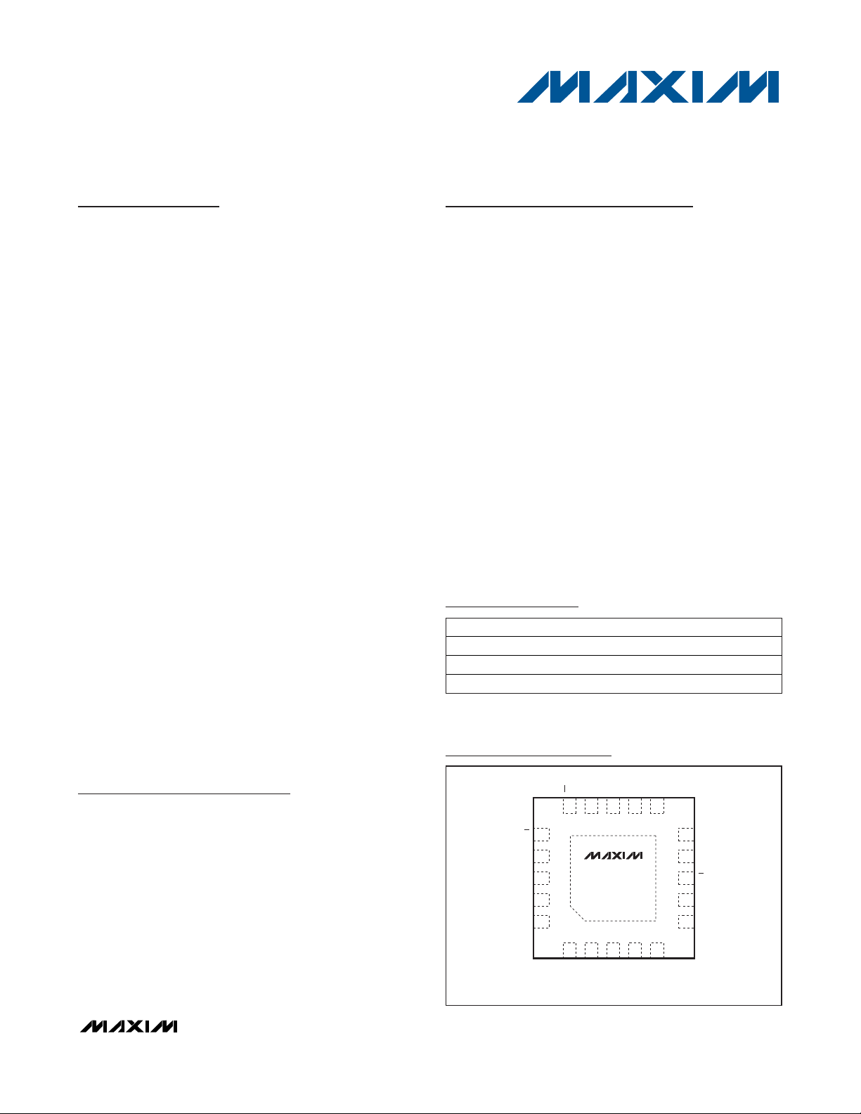
Pin Configuration
Ordering Information
+
Denotes a lead-free/RoHS-compliant package.
*
EP = Exposed pad.
**
Future product—contact factory for availability.
SPI/QSPI are trademarks of Motorola, Inc.
MICROWIRE is a trademark of National Semiconductor Corp.
PART TEMP RANGE PIN-PACKAGE
MAX1377ATP+ -40°C to +125°C 20 TQFN-EP*
MAX1379ATP+ -40°C to +125°C 20 TQFN-EP*
MAX1383ATP+** -40°C to +125°C 20 TQFN-EP*
TOP VIEW
S/D
SEL
AGND
AIN1B
AIN1A
16
17
18
19
20
CNVST
CS
15 14 12 11
MAX1377
MAX1379
MAX1383
(EXPOSED PAD)*
+
DOUT1
SCLK
13
DOUT2
V
10
L
DGND
9
8
U/B
AIN2B
7
AIN2A
6
12
REFSEL
*CONNECT PAD TO AGND
45
3
REF
RGND
TQFN
AGND
AVDD
Page 2
MAX1377/MAX1379/MAX1383
Dual, 12-Bit, 1.25Msps Simultaneous-Sampling
ADCs with Serial Interface
2 _______________________________________________________________________________________
ABSOLUTE MAXIMUM RATINGS
Stresses beyond those listed under “Absolute Maximum Ratings” may cause permanent damage to the device. These are stress ratings only, and functional
operation of the device at these or any other conditions beyond those indicated in the operational sections of the specifications is not implied. Exposure to
absolute maximum rating conditions for extended periods may affect device reliability.
AVDD to AGND ........................................................-0.3V to +6V
V
L
to DGND ..............................................................-0.3V to +6V
SCLK, CS, CNVST, U/B, S/D, SEL,
REFSEL to DGND.......................................-0.3V to (V
L
+ 0.3V)
DOUT_ to DGND...........................................-0.3V to (V
L
+ 0.3V)
AIN1A, AIN1B, AIN2A, AIN2B to AGND
MAX1377/MAX1379 .............................-0.3V to (AVDD + 0.3V)
MAX1383 ..............................................................-12V to +12V
RGND to AGND.....................................................-0.3V to +0.3V
RGND to DGND.....................................................-0.3V to +0.3V
DGND to AGND.....................................................-0.3V to +0.3V
Maximum Current into Any Pin (except power-supply pins).....50mA
Continuous Power Dissipation (T
A
= +70°C)
20-Pin Thin QFN (derate 34.5mW/°C above +70°C) ...2758.6mW
Operating Temperature Range .........................-40°C to +125°C
Junction Temperature......................................................+150°C
Storage Temperature Range .............................-60°C to +150°C
Lead Temperature (soldering, 10s) .................................+300°C
ELECTRICAL CHARACTERISTICS—MAX1377
(V
AVDD
= 2.7V to 3.6V, VL= 1.8V to AVDD, f
SCLK
= 20MHz (50% duty cycle), V
REF
= 2.048V, REFSEL = VL, S/D = DGND, C
REF
=
1µF; T
A
= T
MIN
to T
MAX
, unless otherwise noted. Typical values are at TA= +25°C.)
PARAMETER SYMBOL CONDITIONS MIN TYP MAX UNITS
DC ACCURACY
Resolution 12 Bits
Relative Accuracy INL (Note 1) -1.25 +1.25 LSB
Differential Nonlinearity DNL -1 +1.5 LSB
Offset Error ±8 LSB
Offset-Error Matching ±12 LSB
Gain Error (Note 2) ±6 LSB
Gain-Error Matching (Note 2) ±6 LSB
Gain Temperature Coefficient ±2 ppm/oC
DC Input Isolation
DYNAMIC SPECIFICATIONS (f
Signal-to-Noise Plus Distortion SINAD
Signal-to-Noise Ratio SNR
Total Harmonic Distortion THD Up to the 5th harmonic -84 -74 dB
Spurious-Free Dynamic Range SFDR -86 -76 dB
Intermodulation Distortion IMD f
Full-Power Bandwidth -3dB point 5 MHz
Full-Linear Bandwidth (S/N + D) > 68dB, 1V input 1 MHz
CONVERSION RATE (Figure 4)
Minimum Conversion Time t
Maximum Throughput Rate
Minimum Throughput Rate for
Full Bandwidth Signal
= 500kHz, 2V
IN
CONV
AIN1A to AIN1B, AIN2A to AIN2B 80
AIN1A to AIN2A, AIN1B to AIN2B 80
sine wave, 1.25Msps, 20MHz f
P-P
Unipolar 66 69.5
Bipolar 67 70
Unipolar 66 70
Bipolar 67 70
= 103.5kHz, f
IN1
16 clock cycles per conversion (Note 3) 0.800 µs
Dual output mode, S/D = 0 1.25
Single output mode, S/D = 1 0.625
(Note 4) 10 ksps
)
SCLK
= 113.5kHz -78 dB
IN2
dB
dB
dB
Msps
Page 3
MAX1377/MAX1379/MAX1383
Dual, 12-Bit, 1.25Msps Simultaneous-Sampling
ADCs with Serial Interface
_______________________________________________________________________________________ 3
ELECTRICAL CHARACTERISTICS—MAX1377 (continued)
(V
AVDD
= 2.7V to 3.6V, VL= 1.8V to AVDD, f
SCLK
= 20MHz (50% duty cycle), V
REF
= 2.048V, REFSEL = VL, S/D = DGND, C
REF
=
1µF; T
A
= T
MIN
to T
MAX
, unless otherwise noted. Typical values are at TA= +25°C.)
PARAMETER SYMBOL CONDITIONS MIN TYP MAX UNITS
Track-and-Hold Acquisition Time t
Aperture Delay 2ns
Aperture-Delay Matching 2ns
Aperture Jitter (Note 5) 30 ps
External Clock Frequency f
ANALOG INPUTS (AIN1A, AIN1B, AIN2A, AIN2B)
Input Range U/B = 0, V
Differential Input Range U/B = 1, V
Absolute Voltage Range 0 AVDD V
DC Leakage Current ±1 µA
Input Impedance 34 kΩ
Input Capacitance At each analog input 16 pF
EXTERNAL REFERENCE (REFSEL = 1)
Absolute Input Voltage Range V
Input Capacitance 50 pF
DC Leakage Current ±1 µA
Input Current Time averaged at maximum throughput rate 800 µA
INTERNAL REFERENCE (REFSEL = 0)
Reference Voltage Level 2.028 2.048 2.068 V
Load Regulation
Voltage Temperature Coefficient ±50.0 ppm/oC
DIGITAL INPUTS (SCLK, CNVST, U/B, S/D, SEL, REFSEL)
Input-Voltage Low V
Input-Voltage High V
Input Leakage Current I
DIGITAL OUTPUT (DOUT1, DOUT2)
Output Load Capacitance C
Output-Voltage Low V
Output-Voltage High V
Output Leakage Current I
POWER REQUIREMENTS
Analog Supply Voltage AVDD 2.7 3.0 3.6 V
Digital Supply Voltage V
ACQ
SCLK
REF
IL
IH
IL
DOUT
OL
OH
OL
L
- RGND 0 V
AIN_A
- V
AIN_A
I
I
For stated timing performance 30 pF
I
I
High-impedance mode (Figure 9) ±0.2 µA
= 0 to 1mA 1
SOURCE
= 0 to 50µA 1
SINK
= 5mA 0.4 V
SINK
= 1mA, VL ≥ 2.7V
SOURCE
AIN_B
125 ns
-V
/2 +V
REF
1.0
0.7 x
V
L
V
L
- 0.5V
1.8 AVDD V
AVDD
+ 0.05
0.3 x
20 MHz
REF
REF
V
±10 µA
/2 V
L
V
V
mV/mA
V
V
V
Page 4
MAX1377/MAX1379/MAX1383
Dual, 12-Bit, 1.25Msps Simultaneous-Sampling
ADCs with Serial Interface
4 _______________________________________________________________________________________
ELECTRICAL CHARACTERISTICS—MAX1377 (continued)
(V
AVDD
= 2.7V to 3.6V, VL= 1.8V to AVDD, f
SCLK
= 20MHz (50% duty cycle), V
REF
= 2.048V, REFSEL = VL, S/D = DGND, C
REF
=
1µF; T
A
= T
MIN
to T
MAX
, unless otherwise noted. Typical values are at TA= +25°C.)
ELECTRICAL CHARACTERISTICS—MAX1379
(V
AVDD
= 4.75V to 5.25V, VL= 3V, f
SCLK
= 20MHz (50% duty cycle), V
REF
= 4.096V, REFSEL = VL, S/D = DGND, C
REF
= 1µF; TA=
T
MIN
to T
MAX
, unless otherwise noted. Typical values are at TA= +25°C.)
PARAMETER SYMBOL CONDITIONS MIN TYP MAX UNITS
Analog Supply Current I
Average Static Supply Current 810mA
Digital Supply Current I
Power-Supply Rejection PSR V
DC ACCURACY
Resolution 12 Bits
Relative Accuracy INL (Note 1) -1.25 +1.25 LSB
Differential Nonlinearity DNL -1 +1 LSB
Offset Error ±8 LSB
Offset-Error Matching ±9 LSB
Gain Error (Note 2) ±6 LSB
Gain-Error Matching (Note 2) ±9 LSB
Gain Temperature Coefficient ±2 ppm/oC
DC Input Isolation
DYNAMIC SPECIFICATIONS (f
Signal-to-Noise Plus Distortion SINAD
Signal-to-Noise Ratio SNR
Total Harmonic Distortion THD Up to the 5th harmonic -84 -76 dB
Spurious-Free Dynamic Range SFDR -84 -76 dB
Intermodulation Distortion IMD f
Full-Power Bandwidth -3dB point 5 MHz
Full-Linear Bandwidth (S/N + D) > 68dB, 1V input 1 MHz
CONVERSION RATE (Figure 6)
Minimum Conversion Time t
Maximum Throughput Rate
Minimum Throughput Rate for
Full Bandwidth Signal
PARAMETER SYMBOL CONDITIONS MIN TYP MAX UNITS
AVDD
VL
= 500kHz , 4V
IN
CONV
Normal operation 13 15
Partial power-down mode (Note 5) 2
Full power-down mode (Note 5) 1 5 µA
f
= 20MHz, VL = 3V, CL = 30pF 1 1.5 mA
SCLK
= 3V ±10%, full-scale input ±0.2 ±3 mV
AVDD
AIN1A to AIN1B, AIN2A to AIN2B 80
AIN1A to AIN2A, AIN1B to AIN2B 80
sine wave, 1.25Msps, 20MHz f
P-P
Unipolar 69 70
Bipolar 70 71
Unipolar 70 71
Bipolar 70 72
= 103.5kHz, f
IN1
16 clock cycles per conversion (Note 3) 0.8 µs
Dual-output mode, S/D = 0 1.25
Single-output mode, S/D = 1 0.625
(Note 4) 10 ksps
= 113.5kHz -78 dB
IN2
)
SCLK
mA
dB
dB
dB
Msps
Page 5
MAX1377/MAX1379/MAX1383
Dual, 12-Bit, 1.25Msps Simultaneous-Sampling
ADCs with Serial Interface
_______________________________________________________________________________________ 5
ELECTRICAL CHARACTERISTICS—MAX1379 (continued)
(V
AVDD
= 4.75V to 5.25V, VL= 3V, f
SCLK
= 20MHz (50% duty cycle), V
REF
= 4.096V, REFSEL = VL, S/D = DGND, C
REF
= 1µF; TA=
T
MIN
to T
MAX
, unless otherwise noted. Typical values are at TA= +25°C.)
Track-and-Hold Acquisition Time t
Aperture Delay 2ns
Aperture-Delay Matching 2ns
Aperture Jitter (Note 5) 30 ps
External Clock Frequency f
ANALOG INPUTS (AIN1A, AIN1B, AIN2A, AIN2B)
Input Range U/B = 0, V
Differential Input Range U/B = 1, V
Absolute Voltage Range 0 AVDD V
DC Leakage Current ±1 µA
Input Impedance 34 kΩ
Input Capcitance At each analog input 16 pF
EXTERNAL REFERENCE (REFSEL = 1)
Absolute Input Voltage Range V
Input Capacitance 50 pF
DC Leakage Current ±1 µA
Input Current Time averaged at maximum throughput rate 800 µA
INTERNAL REFERENCE (REFSEL = 0)
Reference Voltage Level 4.086 4.096 4.106 V
Load Regulation
Voltage Temperature Coefficient ±50.0 ppm/oC
DIGITAL INPUTS (SCLK, CNVST, U/B, S/D, SEL, REFSEL)
Input-Voltage Low V
Input-Voltage High V
Input Leakage Current I
DIGITAL OUTPUT (DOUT1, DOUT2)
Output Load Capacitance C
Output-Voltage Low V
Output-Voltage High V
Output Leakage Current I
POWER REQUIREMENTS
Analog Supply Voltage AVDD 4.25 5.0 5.25 V
Digital Supply Voltage V
PARAMETER SYMBOL CONDITIONS MIN TYP MAX UNITS
ACQ
SCLK
REF
I
SOURCE
= 0 to 50µA 1
I
SINK
IL
IH
IL
DOUT
OH
OL
For stated timing performance 30 pF
I
OL
L
= 5mA 0.4 V
SINK
I
SOURCE
High-impedance mode (Figure 9) ±0.2 µA
125 ns
- RGND 0 V
AIN_A
- V
AIN_A
= 0 to 1mA 1
= 1mA, VL ≥ 2.7V
AIN_B
-V
/2 + V
REF
1.0
0.7 x
V
L
V
-
L
0.5V
1.8 AVDD V
20 MHz
REF
/2
R E F
AVDD
+ 0.05
mV/mA
0.3 x
V
L
±10 µA
V
V
V
V
V
Page 6
MAX1377/MAX1379/MAX1383
Dual, 12-Bit, 1.25Msps Simultaneous-Sampling
ADCs with Serial Interface
6 _______________________________________________________________________________________
ELECTRICAL CHARACTERISTICS—MAX1379 (continued)
(V
AVDD
= 4.75V to 5.25V, VL= 3V, f
SCLK
= 20MHz (50% duty cycle), V
REF
= 4.096V, REFSEL = VL, S/D = DGND, C
REF
= 1µF; TA=
T
MIN
to T
MAX
, unless otherwise noted. Typical values are at TA= +25°C.)
TIMING CHARACTERISTICS (Figures 6, 10)
V
AVDD
= 4.25V to 5.25V, VL= 1.8V to AVDD, V
REF
= 4.096V, f
SCLK
= 20MHz for MAX1379, 50% duty cycle, CL= 30pF, TA= T
MIN
to
T
MAX
, unless otherwise noted. Typical values are at TA= +25°C.)
Note 1: Relative accuracy is the deviation of the analog value at any code from its theoretical value after the gain error and the offset
error have been nulled.
Note 2: Offset nulled.
Note 3: Conversion time is defined as the number of clock cycles (16) multiplied by the clock period. Clock has 50% duty cycle.
Note 4: At sample rates below 10ksps, the input full linear bandwidth is reduced to 5kHz.
Note 5: SCLK and CNVST not switching during measurement.
Analog Supply Current I
Average Static Current 910mA
Digital Supply Current I
Power-Supply Rejection PSR V
SCLK Clock Period t
SCLK Duty Cycle tCH/t
SCLK Pulse-Width High t
SCLK Pulse-Width Low t
SCLK Rise to DOUT_ Transition t
DOUT_ Remains Valid After
SCLK
CNVST Fall to SCLK Fall t
CNVST Pulse Width t
Power-Up Time; Full Power-Down t
SEL to CNVST Fall t
SEL Hold to CNVST Fall 10 ns
CS Fall To CNVST Fall t
Restart Time; Partial Power-Down t
PARAMETER SYMBOL CONDITIONS MIN TYP MAX UNITS
PARAMETER SYMBOL CONDITION MIN TYP MAX UNITS
Normal operation 16 18
AVDD
VL
CP
CH
CL
DOUT
t
DHOLD
SETUP
CSW
PWR-UP
SEL_SETUP
CST
RCV
Partial power-down mode (Note 5) 2
Full power-down mode (Note 5) 5 µA
f
= 20MHz, VL = 5V, CL = 30pF 2 3
SCLK
f
= 20MHz, VL = 3V, CL = 30pF 1
SCLK
= 5V ±10%, full-scale input ±0.2 ±3 mV
AVDD
CL
CL = 30pF, VL = 5V 14
CL = 30pF, VL = 3V 17
CL = 30pF, VL = 1.8V 24
CL = 30pF 10 ns
External load on REF < 3µF 2 ms
External load on REF < 3µF 2 ms
No external load 16 Cycles
50 ns
45 55 %
22.5 ns
22.5 ns
4ns
20 ns
100 120 ns
mA
mA
ns
Page 7
MAX1377/MAX1379/MAX1383
Dual, 12-Bit, 1.25Msps Simultaneous-Sampling
ADCs with Serial Interface
_______________________________________________________________________________________ 7
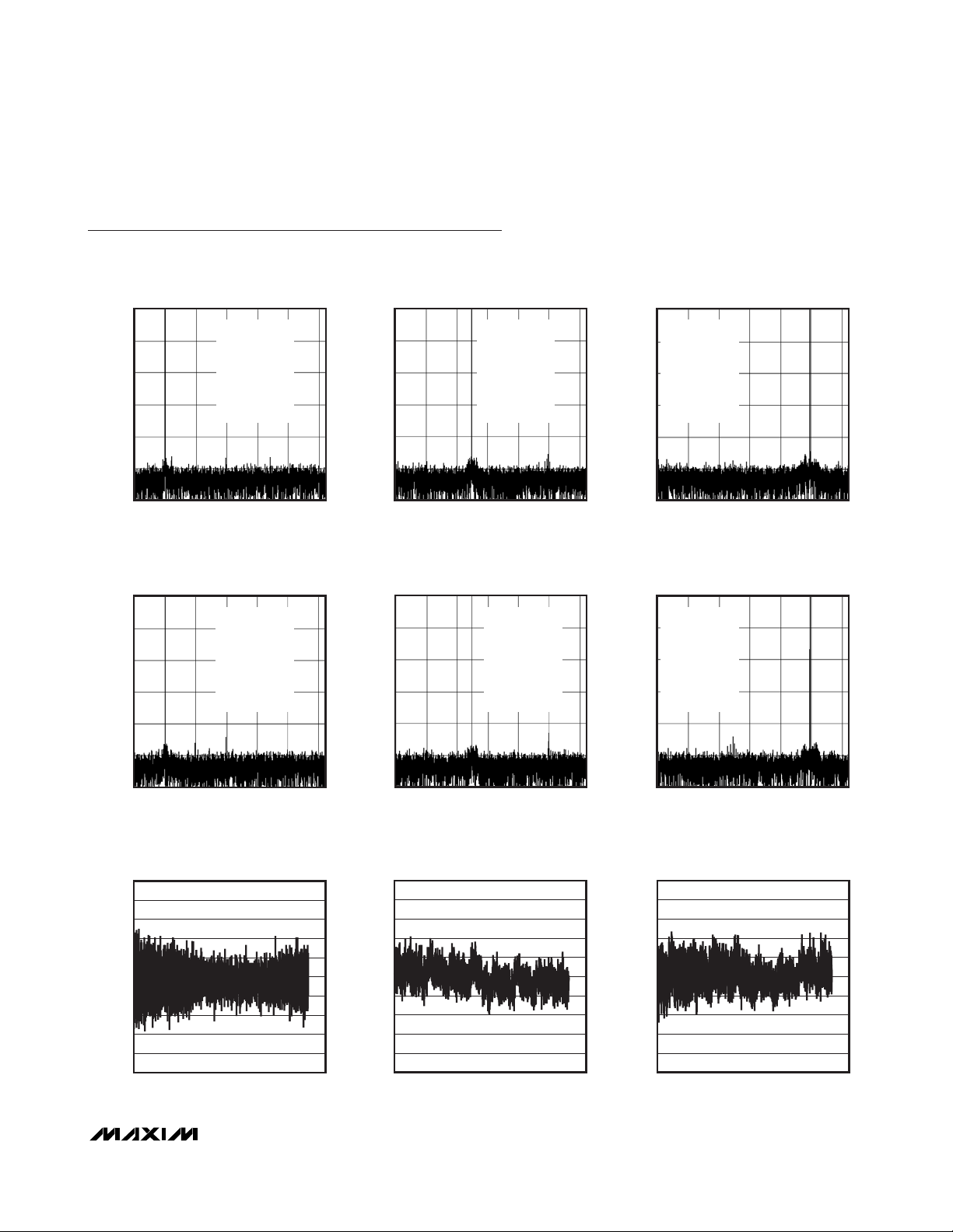
Typical Operating Characteristics
(V
AVDD
= 5V/3V, VL= 3V, f
SCLK
= 20MHz, TA= +25°C, unless otherwise noted.)
0
-20
-40
-60
AMPLITUDE (dB)
-80
-100
-120
0 100 200 300 400 500 600
0
-20
-40
-60
AMPLITUDE (dB)
-80
MAX1377 BIPOLAR FFT
f
= 1.25MHz
SAMPLE
f
= 20MHz
SCLK
f
= 100kHz
IN
SINAD = 60.052dB
SNR = 69.073dB
THD = -92.267dB
SFDR = 93.225dB
V
= 2.048V
REF
ANALOG INPUT FREQUENCY (kHz)
MAX1377 UNIPOLAR FFT
f
= 1.25MHz
SAMPLE
f
= 20MHz
SCLK
f
= 100kHz
IN
SINAD = 69.324dB
SNR = 69.400dB
THD = -86.952dB
SFDR = 89.213dB
V
= 2.048V
REF
MAX1377 toc01
MAX1377 toc04
MAX1377 BIPOLAR FFT
0
f
= 1.25MHz
-20
-40
-60
AMPLITUDE (dB)
-80
-100
-120
0 100 200 300 400 500 600
ANALOG INPUT FREQUENCY (kHz)
MAX1377 UNIPOLAR FFT
0
-20
-40
-60
AMPLITUDE (dB)
-80
SAMPLE
f
= 20MHz
SCLK
f
= 250kHz
IN
SINAD = 68.720dB
SNR = 68.769dB
THD = -88.244dB
SFDR = 91.237dB
V
= 2.048V
REF
f
SAMPLE
f
= 20MHz
SCLK
f
= 250kHz
IN
SINAD = 68.947dB
SNR = 69.054dB
THD = -85.101dB
SFDR = 86.718dB
= 2.048V
V
REF
= 1.25MHz
MAX1377 toc02
MAX1377 toc05
MAX1377 BIPOLAR FFT
0
f
= 1.25MHz
SAMPLE
-20
-40
-60
AMPLITUDE (dB)
-80
-100
-120
= 20MHz
f
SCLK
f
= 500kHz
IN
SINAD = 68.542dB
SNR = 68.554dB
THD = -90.391dB
SFDR = 94.350dB
V
= 2.048V
REF
0 100 200 300 400 500 600
ANALOG INPUT FREQUENCY (kHz)
MAX1377 UNIPOLAR FFT
0
f
= 1.25MHz
SAMPLE
-20
f
= 20MHz
SCLK
f
= 500kHz
IN
SINAD = 68.645dB
-40
SNR = 68.715dB
THD = -83.617dB
-60
SFDR = 88.709dB
V
= 2.048V
REF
AMPLITUDE (dB)
-80
MAX1377 toc03
MAX1377 toc06
-100
-120
0 100 200 300 400 500 600
ANALOG INPUT FREQUENCY (kHz)
MAX1377 UNIPOLAR DNL
vs. OUTPUT CODE
1.0
0.8
0.6
0.4
0.2
0
DNL (LSB)
-0.2
-0.4
-0.6
-0.8
-1.0
500 3500 4000
0 45002000 2500 30001000 1500
CODE
MAX1377 toc07
-100
-120
0 100 200 300 400 500 600
ANALOG INPUT FREQUENCY (kHz)
MAX1377 BIPOLAR INL
vs. OUTPUT CODE
1.0
0.8
0.6
0.4
0.2
0
INL (LSB)
-0.2
-0.4
-0.6
-0.8
-1.0
CODE
300025001000 200015005000
3500 45004000
MAX1377 toc08
-100
-120
0 100 200 300 400 500 600
ANALOG INPUT FREQUENCY (kHz)
MAX1377 UNIPOLAR INL
vs. OUTPUT CODE
1.0
0.8
0.6
0.4
0.2
0
INL (LSB)
-0.2
-0.4
-0.6
-0.8
-1.0
CODE
MAX1377 toc09
3500 45004000300025001000 200015005000
Page 8

MAX1377/MAX1379/MAX1383
Dual, 12-Bit, 1.25Msps Simultaneous-Sampling
ADCs with Serial Interface
8 _______________________________________________________________________________________
Typical Operating Characteristics (continued)
(V
AVDD
= 5V/3V, VL= 3V, f
SCLK
= 20MHz, TA= +25°C, unless otherwise noted.)
MAX1379 FFT PLOT
MAX1377 toc18
ANALOG INPUT FREQUENCY (kHz)
AMPLITUDE (dB)
0 300 600 900
0
-20
-40
-60
-80
-100
-120
f
SAMPLE
= 1.8Msps
f
SCLK
= 28.8MHz
f
IN
= 250kHz
SINAD = 70.05dB
SNR = 70.32dB
THD = -82.35dB
SFDR = 83.22dB
V
REF
= 4.096V
MAX1377 BIPOLAR DNL
vs. OUTPUT CODE
1.0
0.8
0.6
0.4
0.2
0
DNL (LSB)
-0.2
-0.4
-0.6
-0.8
-1.0
3500 45004000300025001000 200015005000
CODE
MAX1377 toc10
INL (LSB)
MAX1379 UNIPOLAR DIFFERENTIAL
NONLINEARITY vs. DIGITAL OUTPUT CODE
1.0
0.8
0.6
0.4
0.2
0
DNL (LSB)
-0.2
-0.4
-0.6
-0.8
-1.0
0 4096
DIGITAL OUTPUT CODE (LSB)
307220481024
MAX1377 toc13
DNL (LSB)
MAX1379 UNIPOLAR INTEGRAL
NONLINEARITY vs. DIGITAL OUTPUT CODE
1.0
0.8
0.6
0.4
0.2
0
-0.2
-0.4
-0.6
-0.8
-1.0
0 4096
DIGITAL OUTPUT CODE (LSB)
307220481024
MAX1379 BIPOLAR DIFFERENTIAL
NONLINEARITY vs. DIGITAL OUTPUT CODE
1.0
0.8
0.6
0.4
0.2
0
-0.2
-0.4
-0.6
-0.8
-1.0
0 4096
DIGITAL OUTPUT CODE (LSB)
307220481024
MAX1377 toc11
MAX1377 toc14
MAX1379 BIPOLAR INTEGRAL
NONLINEARITY vs. DIGITAL OUTPUT CODE
1.0
0.8
0.6
0.4
0.2
0
INL (LSB)
-0.2
-0.4
-0.6
-0.8
-1.0
0 4096
DIGITAL OUTPUT CODE (LSB)
307220481024
MAX1379 OFFSET ERROR
vs. TEMPERATURE
0
-0.3
-0.6
-0.9
OFFSET ERROR (LSB)
-1.2
CHANNEL 2
-1.5
-40 10-15 35 60 85
CHANNEL 1
TEMPERATURE (°C)
MAX1377 toc12
MAX1377 toc15
MAX1379 GAIN ERROR
2.0
1.6
1.2
0.8
GAIN ERROR (LSB)
0.4
0
-40 10-15 35 60 85
vs. TEMPERATURE
CHANNEL 2
CHANNEL 1
TEMPERATURE (°C)
MAX1377 toc16
MAX1379 FFT PLOT
0
f
= 1.8Msps
-20
-40
-60
AMPLITUDE (dB)
-80
-100
-120
SAMPLE
f
= 28.8MHz
SCLK
f
= 100kHz
IN
SINAD = 70.43dB
SNR = 70.72dB
THD = -82.33dB
SFDR = 82.78dB
V
= 4.096V
REF
0 300 600 900
ANALOG INPUT FREQUENCY (kHz)
MAX1377 toc17
Page 9

MAX1377/MAX1379/MAX1383
Dual, 12-Bit, 1.25Msps Simultaneous-Sampling
ADCs with Serial Interface
_______________________________________________________________________________________ 9
Typical Operating Characteristics (continued)
(V
AVDD
= 5V/3V, VL= 3V, f
SCLK
= 20MHz, TA= +25°C, unless otherwise noted.)
0
-20
-40
-60
AMPLITUDE (dB)
-80
-100
-120
0 400 600 800200
0
-20
-40
-60
AMPLITUDE (dB)
-80
-100
-120
0 300 600 900
MAX1379 FFT PLOT
f
= 1.8Msps
SAMPLE
= 28.8MHz
f
SCLK
fIN = 300kHz
SINAD = 70dB
SNR = 70.27dB
THD = -82.2dB
SFDR = 81.81dB
V
= 4.096V
REF
ANALOG INPUT FREQUENCY (kHz)
MAX1379 INTERMODULATION PLOT
f
= 1.8Msps
SAMPLE
f
= 28.8MHz
SCLK
= 250kHz
f
IN1
f
= 300kHz
IN1
IMD = -81.53dB
= 4.096V
V
REF
ANALOG INPUT FREQUENCY (kHz)
MAX1379 TOTAL HARMONIC DISTORTION
vs. SOURCE IMPEDENCE
-72
-74
-76
-78
-80
-82
TOTAL HARMONIC DISTORTION (dBc)
-84
-86
10 1000
SOURCE IMPEDANCE (Ω)
fIN = 500kHz
100
MAX1379 AVDD PARTIAL POWER-DOWN
CURRENT vs. TEMPERATURE
4.0
3.8
3.6
3.4
3.2
3.0
2.8
2.6
2.4
AVDD FULL POWER-DOWN CURRENT (mA)
2.2
2.0
-40 -10 5 20-25 35 50 65 80
TEMPERATURE (°C)
MAX1377 toc19
MAX1377 toc22
MAX1379 FFT PLOT
0
-20
f
SAMPLE
-40
-60
AMPLITUDE (dB)
-80
-100
-120
0 300 600 900
ANALOG INPUT FREQUENCY (kHz)
f
SCLK
= 500kHz
f
IN
SINAD = 69.58dB
SNR = 69.75dB
THD = -83.79dB
SFDR = 84.69dB
V
REF
MAX1379 AVDD FULL POWER-DOWN
CURRENT vs. TEMPERATURE
1.0
0.9
0.8
0.7
0.6
0.5
0.4
0.3
0.2
0.1
0
-40 -10 5 20-25 35 50 65 80
TEMPERATURE (°C)
= 1.8Msps
MAX1377 toc20
= 28.8MHz
= 4.096V
MAX1377 toc23
MAX1377 toc21
fIN = 100kHz
MAX1377 toc24
MAX1379 AVDD SUPPLY CURRENT
vs. TEMPERATURE
14.0
13.5
13.0
12.5
12.0
11.5
11.0
AVDD SUPPLY CURRENT (mA)
10.5
10.0
-40 5 20-25 -10 35 50 65 80
TEMPERATURE (°C)
MAX1377 toc25
MAX1379 AVDD SUPPLY CURRENT
vs. CONVERSION RATE
20
18
16
14
12
10
8
6
AVDD SUPPLY CURRENT (mA)
4
2
0
0 800400 1200 1600 2000
CONVERSION RATE (kHz)
MAX1377 toc26
Page 10
MAX1377/MAX1379/MAX1383
Dual, 12-Bit, 1.25Msps Simultaneous-Sampling
ADCs with Serial Interface
10 ______________________________________________________________________________________
Typical Operating Characteristics (continued)
(V
AVDD
= 5V/3V, VL= 3V, f
SCLK
= 20MHz, TA= +25°C, unless otherwise noted.)
MAX1379 FULL-SCALE AMPLITUDE
vs. FREQUENCY
(V)
V
REF
4.10
4.09
4.08
4.07
4.06
4.05
4.04
4.03
4.02
4.01
3850
3800
3750
3700
3650
OUTPUT SWING (LSB)
3600
3550
110
FREQUENCY (MHz)
MAX1377 toc27
MAX1379 INTERNAL REFERENCE VOLTAGE
vs. ANALOG SUPPLY VOLTAGE
MAX1377 toc28
TA = +25°C
TA = -40°C
TA = +85°C
4.20 4.70 5.204.45 4.95
AVDD (V)
Page 11
MAX1377/MAX1379/MAX1383
Dual, 12-Bit, 1.25Msps Simultaneous-Sampling
ADCs with Serial Interface
______________________________________________________________________________________ 11
Pin Description
PIN NAME FUNCTION
1 REFSEL
2 REF
3 RGND
4, 18 AGND Analog Ground
5 AVDD Analog-Supply Input. Bypass AVDD with a 10µF || 10nF capacitor to ground.
6 AIN2A
7 AIN2B
8 U/B
9 DGND Digital Supply Ground
10 V
11 DOUT2 Serial-Data Output 2. Data is clocked out on the rising edge of SCLK.
12 DOUT1 Serial-Data Output 1. Data is clocked out on the rising edge of SCLK.
13 SCLK Serial-Clock Input. Clocks data out of the serial interface. SCLK also sets the conversion time.
14 CNVST
15 CS
16 S/D
17 SEL
19 AIN1B
20 AIN1A
— EP Exposed Pad. EP is internally connected to AGND.
L
Reference-Select Input. Drive REFSEL high to select external reference mode and power down the
internal reference. Drive REFSEL low to select internal reference mode.
Internal Reference Output/External Reference Input. For internal reference mode, bypass REF to
RGND with a ≥ 1µF capacitor. For external reference mode, apply a reference voltage at REF.
Reference Ground/Common Negative Input. In bipolar mode, RGND is the reference ground. In
unipolar mode, RGND is the common negative input for all four analog inputs (see Figure 3).
Primary/Positive Analog Input Channel 2. AIN2A is the primary channel 2 input (AIN2A) if using
single-ended inputs (U/B is low) and the positive channel 2 input (AIN2+) if using differential inputs
(U/B is high) (see Figure 3).
Secondary/Negative Analog Input Channel 2. AIN2B is the secondary channel 2 input (AIN2B) if
using single-ended inputs (U/B is low) and the negative channel 2 input (AIN2-) if using differential
inputs (U/B is high) (see Figure 3).
Unipolar/Bipolar Input. Drive U/B low to select unipolar mode. Drive U/B high to select bipolar
mode. In bipolar mode, the analog inputs are differential.
Digital Supply Input. Bypass VL with a 10µF || 10nF capacitor to ground.
Conversion-Start Input. Forcing CNVST high prepares the device for a conversion. Conversion
begins on the falling edge of CNVST.
Active-Low, Chip-Select Input. Drive CS low to enable the serial interface. When CS is high, DOUT1
and DOUT2 are high impedance, the serial interface resets, and the device powers down.
Single-Output/Dual-Output Selection Input. Drive S/D high to route ADC2 data through DOUT1 after
ADC1 data. Drive S/D low for dual outputs with ADC1 data going to DOUT1 and ADC2 data going
D
to DOUT2. See the Single-/Dual-Output Modes (S/
Analog-Input Selection Input. If U/B is low (unipolar mode), drive SEL low to select the primary
inputs, AIN1A and AIN2A. Drive SEL high to select the secondary inputs, AIN1B and AIN2B. In
bipolar mode, SEL is ignored.
Secondary/Negative Analog Input Channel 1. AIN1B is the secondary channel 1 input (AIN1B) if
using single-ended inputs (U/B is low) and the negative channel 1 input (AIN1-) if using differential
inputs (U/B is high) (see Figure 3).
Primary/Positive Analog Input Channel 1. AIN1A is the primary channel 1 input (AIN1A) if using
single-ended inputs (U/B is low) and the positive channel 1 input (AIN1+) if using differential inputs
(U/B is high) (see Figure 3).
) section.
Page 12
MAX1377/MAX1379/MAX1383
Dual, 12-Bit, 1.25Msps Simultaneous-Sampling
ADCs with Serial Interface
12 ______________________________________________________________________________________
Detailed Description
The MAX1377/MAX1379/MAX1383 use an input track
and hold (T/H) and SAR circuitry to convert an analog
input signal to a digital 12-bit output. The dual serial
interface requires a minimum of three digital lines
(SCLK, CNVST, and DOUT) and provides easy interfacing to microprocessors (µPs) and DSPs. Four digital
lines are required for dual-output mode.
Input T/H Circuit
Upon power-up, the input T/H circuit enters its tracking
mode immediately. Following a conversion, the T/H
enters the tracking mode on the 14th SCLK rising edge
of the previous conversion (Figure 6). The T/H enters
the hold mode on the falling edge of CNVST. The time
required for the T/H to acquire an input signal is determined by how quickly the input capacitance is
charged. If the input signal’s source impedance is high,
the acquisition time lengthens. The acquisition time,
t
ACQ
, is the minimum time needed for the signal to be
acquired (see the
Definitions
section). t
ACQ
is calculat-
ed by the following equation:
t
ACQ
≥ 9 x (RS + RIN) x C
IN
where RIN= 450Ω, CIN= 16pF, and RSis the source
impedance of the input signal.
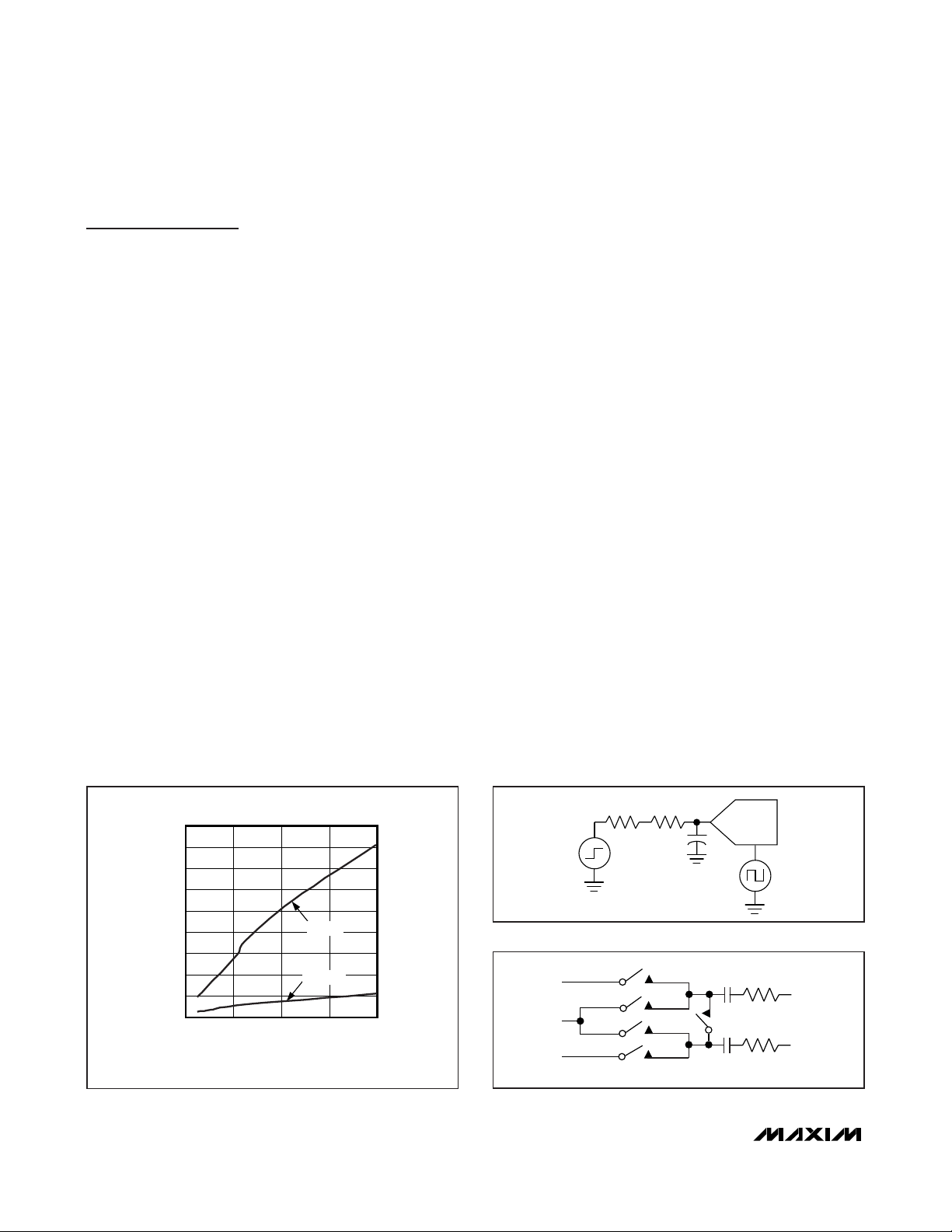
Figure 1 shows the acquisition time as tested using the
circuit of Figure 2. The acquisition time is the time
between the rising edge of a 1V to 3V step input and
the falling edge of CONVST which produced a stable
sample. Rs represents the source impedance of the
function generator (50Ω) and Rx represents the variable filter resistance.
Unipolar Mode
The MAX1377/MAX1379/MAX1383 support two simultaneously sampled, single-ended conversions in unipolar
mode. Drive U/B low for unipolar mode. In unipolar
mode, switches A–D in Figure 3 close according to the
position of SEL. Drive SEL low to close switches A and
D and designate AIN1A and AIN2A as the active, single-ended inputs referenced to RGND. Drive SEL high
to close switches B and D and select AIN1B and AIN2B
as the active, single-ended inputs referenced to RGND.
The output code in unipolar mode is straight binary.
See Figure 4 for the unipolar transfer function.
Bipolar Mode
Drive U/B high to configure the inputs for bipolar/differential mode. Switches A and C in Figure 3 are closed,
designating AIN1A (AIN2A) and AIN1B (AIN2B) as the
active, differential inputs. In bipolar mode, SEL is
ignored. The output code is in two’s complement.
Figure 5 shows the transfer function for bipolar mode.
Input Bandwidth
The ADC’s input-tracking circuitry has a 5MHz smallsignal bandwidth, allowing the ADC to digitize highspeed transient events and measure periodic signals
with bandwidths exceeding the ADC’s sampling rate by
using undersampling techniques. To avoid high-frequency signals being aliased into the frequency band
of interest, anti-alias filtering is recommended.
Analog Input Protection
Internal protection diodes that clamp the analog input
to AVDD and AGND allow the analog inputs to swing
from AGND - 0.3V to AVDD + 0.3V without damage to
Figure 3. Equivalent Input Circuit
Figure 2. Test Circuit
Figure 1. Acquisition Time vs. Source Impedance
RxRs
1800
1600
1400
1200
1000
800
600
ACQUISITION TIME (ns)
400
200
0
0 200
SOURCE IMPEDANCE, Rx (Ω)
C = 1nF
C = 120pF
15010050
MAX1377 fig01
AIN1A
(AIN2A)
AIN1B
(AIN2B)
RGND
1V TO 3V
STEP
C
A
B
C
D
C
C
ADC
CONVST
R
IN
IN
TO ADC+
R
IN
IN
TO ADC-
Page 13

MAX1377/MAX1379/MAX1383
Dual, 12-Bit, 1.25Msps Simultaneous-Sampling
ADCs with Serial Interface
______________________________________________________________________________________ 13
the MAX1377 and MAX1379. The MAX1383 can handle
±10V input swings. All inputs must not exceed the stated ranges for accurate conversions.
Internal Reference Mode
Drive REFSEL low to select internal reference mode. The
MAX1377 includes an on-chip 2.048V reference; the
MAX1379 has a 4.096V reference; and the MAX1383
includes a 2.5V internal reference. The reference output
at REF can be used as a reference voltage source for
other components. REF can source up to 2mA. Bypass
REF with a 10nF capacitor and a 4.7µF capacitor to
RGND. It is important to select a low ESR capacitor and
keep the trace resistance as low as possible.
The internal reference is continuously powered-up during both normal and partial power-down modes. In full
power-down mode, the internal reference is disabled.
Allow at least 2ms recovery time after a power-on reset
or exiting full power-down mode for the reference to
settle to its intended value.
Input Voltage Range (MAX1383)
The input range on the MAX1383 has an 8x relationship
with the reference voltage. For example, when the reference voltage (internal or external) is 2.5V, the input
range is ±10V (20V
P-P
).
External Reference Mode
Drive REFSEL high to select external reference mode.
Apply a reference voltage at REF. Bypass REF with
a 10nF capacitor and a 4.7µF capacitor to RGND. As
with the internal reference, it is important to select a low
ESR capacitor and keep the trace resistance as low
as possible.
Serial Interface
Initialization After Power-Up
Upon initial power-up, the MAX1377/MAX1379/ MAX1383
require a complete conversion cycle to initialize the internal calibration. Following this initialization, the ADC is
ready for normal operation. This initialization is only
required after a hardware power-on reset and is not
required after exiting partial or full power-down mode.
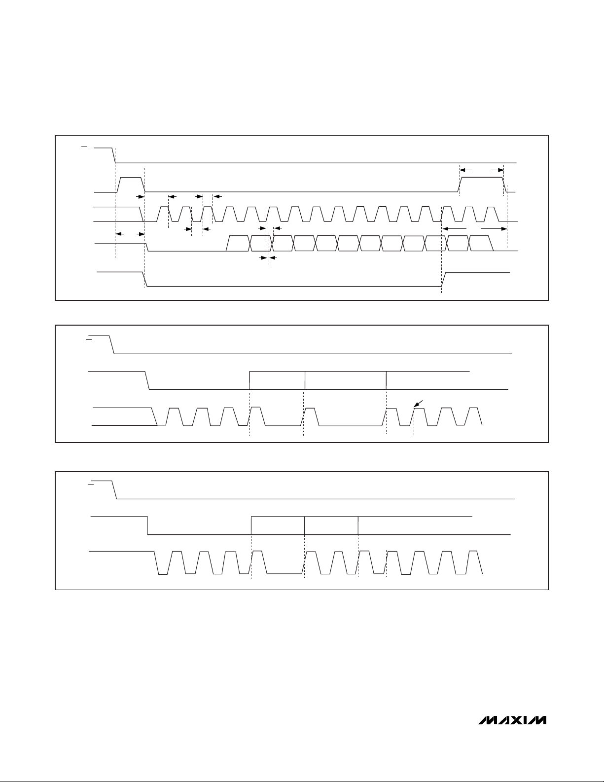
Starting a Conversion and Reading the Output
With SCLK idling high or low, a falling edge on CNVST
begins a conversion (see Figure 6). This causes the
analog input stage to transition from track to hold
mode. SCLK provides the timing for the conversion
process, and data is shifted out as each bit of the result
is determined. A rising edge in CNVST forces the
device into one of three modes. The mode is determined by the clock cycle in which the transition occurs
and whether the device is set for single or dual outputs.
Figures 7 and 8 show each mode that is activated with
a rising CNVST edge for single and dual outputs.
DOUT1 (and DOUT2, if S/D = low) transitions from high
impedance to being actively driven low once the ADC
enters hold mode. DOUT_ remains low for the first three
SCLK pulses and begins outputting the conversion result
after the 4th rising edge of SCLK, MSB first. DOUT_ transitions complete t
DOUT
after each SCLK rising edge and
the DOUT_ values remain valid for t
HOLD
after the next
rising edge of SCLK. A total of 16 SCLK pulses are
required to complete a normal conversion in dual-output
mode and 28 SCLK pulses in single-output mode.
DOUT_ goes low after the 16th rising edge of SCLK and
goes high-impedance when CNVST goes high.
Figure 4. Unipolar Transfer Function (U/B = Low)
Figure 5. Bipolar Transfer Function (U/B = High)
FULL-SCALE
TRANSITION
111...111
111...110
111...101
DIGITAL OUTPUT CODE
000...011
000...010
000...001
000...000
0
2
1
3
INPUT VOLTAGE (LSB)
V
FS =
ZS = 0
1 LSB =
FS
FS - 3/2 LSB
REF
V
REF
4096
011...111
011...100
000...010
000...001
000...000
111...111
111...110
DIGITAL OUTPUT CODE
111...101
100...001
100...000
V
- 1 LSB
-FS
REF
DIFFERENTIAL INPUT VOLTAGE (LSB)
FULL-SCALE
TRANSITION
MAX1377/
MAX1379
V
+FS =
ZS = 0
-V
-FS =
1 LSB =
MAX1383
+FS = 4V
ZS = 0
-FS = -4V
8 x V
1 LSB =
+FS
+FS - 3/2 LSB
REF
2
V
4096
4096
REF
2
REF
REF
REF
REF
Page 14
MAX1377/MAX1379/MAX1383
Dual, 12-Bit, 1.25Msps Simultaneous-Sampling
ADCs with Serial Interface
14 ______________________________________________________________________________________
For continuous operation in single-output mode, pull
CNVST high after the 14th rising and before the 28th
rising edge of SCLK. In dual-output mode, if CNVST
returns high after the 14th rising and before the 16th
falling edge of SCLK, DOUT_ remains active so continuous conversions can be sustained. If CNVST is low
during the 16th edge of SCLK (dual-conversion mode)
and the 28th falling edge of SCLK (single-output mode),
DOUT_ returns to its high-impedance state on the next
rising edge of CNVST or SCLK, enabling the serial interface to be shared by multiple devices. See Figures 9
and 10 for single and continuous conversion timing
diagrams.
Figure 6. Detailed Serial-Interface Timing Diagram
Figure 7. Single-Output CNVST Transition Modes
Figure 8. Dual-Output CNVST Transition Modes
CS
t
CSW
CNVST
t
SETUP
SCLK
DOUT_
INTERNAL T/H STATE
t
CST
1
CS
t
CH
13
14
D1
t
ACQ
D0
TRACKING
t
CL
D11 D10
t
DHOLD
t
DOUT
D9
HOLD MODE
D7
D8
D5
D6
D3
D4
D2
CNVST
SCLK
3
2
1
POWER-DOWN CONTINUOUS MODE
4
14
CS
CNVST
SCLK
1
3
2
POWER-DOWN CONTINUOUS MODE
4
15
14
DOUT_ HI-Z
16 17
28
DOUT_ HI-Z
DOUT1 HI-Z
DOUT1 GOES HI-Z
29
Page 15

MAX1377/MAX1379/MAX1383
Dual, 12-Bit, 1.25Msps Simultaneous-Sampling
ADCs with Serial Interface
______________________________________________________________________________________ 15
Single-/Dual-Output Modes (S/D)
In dual-output mode, conversion results from the two
channels appear on separate outputs. DOUT1 outputs
the result from channel 1 and DOUT2 outputs the result
from channel 2. Drive S/D low to operate in dual-output
mode. For DSPs with two-buffer and two-input-stream
capability, use the dual-output mode to allow for easier
DSP software for dual streams. Two buffer locations can
be used so the streams do not need to be separated.
In single-output mode, the results from both channels
appear on DOUT1. The channel 2 conversion result follows the channel 1 conversion result (see Figure 10).
The MSB (D11) of the channel 2 conversion result
appears on DOUT1 after the 16th rising edge of SCLK.
The LSB (D0) of the channel 2 conversion result
appears on DOUT1 after the 27th rising edge of SCLK
and is ready to be clocked in on the 28th rising edge of
SCLK. DOUT2 is high-impedance when S/D is high.
If CNVST goes high after the 28th rising edge of SCLK,
DOUT1 goes high impedance until the next conversion
is initiated (single-conversion mode). If CNVST goes
high after the 14th rising edge and before the 28th rising edge of SCLK, DOUT1 is actively driven low until
the next conversion results are ready (continuous- conversion mode).
Note: In single-output mode, the conversion speed is
limited to 0.625Msps by the maximum SCLK.
Power-Down Modes
Partial Power-Down (PPD)
Reduce power consumption by placing the MAX1377/
MAX1379/MAX1383 in partial or full power-down mode.
Partial power-down mode is ideal for infrequent data
sampling and applications requiring fast wake-up
times. Pull CNVST high after the 3rd and before the
14th rising edge of SCLK to place the device in partial
power-down mode. This reduces the analog supply
current to 2mA. While in partial power-down mode, the
internal reference remains enabled (if REFSEL = GND).
Figure 11 shows the timing sequence to enter partial
power-down mode.
Full Power-Down Mode (FPD)
Full power-down mode is ideal for infrequent data sampling and very low-supply current applications. To enter
full power-down mode, place the MAX1377/MAX1379/
MAX1383 first in partial power-down mode. Perform the
Figure 9. Dual-Output Mode, Single and Continuous Conversions
SINGLE CONVERSION
CNVST
SCLK
DOUT_
HIGH-Z
CONTINUOUS CONVERSION
CNVST
SCLK
DOUT_
*CNVST MUST GO HIGH BETWEEN THE 14TH RISING AND 16TH FALLING EDGES OF SCLK.
TO MAINTAIN CONTINUOUS CONVERSIONS, DOUT_ REMAINS LOW BETWEEN
CONVERSION RESULTS IN CONTINUOUS-CONVERSION DUAL-OUTPUT MODE.
1
0
1
0
00
00
D11 D10
D11 D10
D8
D9
D8
D9
8
8
9
D2
D4
D5
D7
D7
D6
9
D4
D5
D6
D3
D3
D1
CONTINUOUS-CONVERSION
SELECTION WINDOW*
D2
D1
16
D0
1614
D0
HIGH-Z
1
Page 16

MAX1377/MAX1379/MAX1383
Dual, 12-Bit, 1.25Msps Simultaneous-Sampling
ADCs with Serial Interface
16 ______________________________________________________________________________________
CNVST/SCLK sequence necessary to enter partial
power-down mode. Repeat the same sequence to enter
full power-down mode. In full power-down mode, the
internal reference is disabled to minimize power consumption. Figure 12 shows the timing sequence to
enter full power-down mode.
Another way to enter the full power-down mode is to
drive CS high. If CS is high, the MAX1377/MAX1379/
MAX1383 act as if the full power-down sequence were
issued. To exit the CS-initiated power-down mode,
drive CS low. Allow 2ms for the reference to wake up
and settle before performing a conversion.
Exiting Partial and Full Power-Down Modes
Drive CNVST low and allow at least 14 SCLK cycles to
elapse before driving CNVST high to exit partial or full
power-down mode. When exiting partial power-down
mode, conversions can begin immediately without having to wait for the reference to wake-up. When exiting
full power-down mode, allow at least 2ms recovery time
after exiting to ensure that the internal reference has
settled.
In partial or full power-down mode, maintain idle SCLK
low or high to minimize power.
Figure 10. Single-Output Mode, Single and Continuous Conversions
Figure 11. Partial Power-Down Timing Sequence
SINGLE CONVERSION
(SINGLE OUTPUT)
CNVST
8
SCLK
1
D10D9D8
000
DOUT1
CONTINUOUS CONVERSION
(SINGLE OUTPUT)
CNVST
SCLK
1
DOUT1
D11
D10D9D8
000
D11
CNVST
SCLK
1
1ST SCLK RISING EDGE
9
D7
D6D5D4
CHANNEL 1
CONVERSION RESULT
8
9
D7
D6
CHANNEL 1
CONVERSION RESULT
39
D3 D2
D5D4D3 D2D1D0
D1
16
17 24
D7
D10D9D8
D11
D0
CONVERSION RESULT
1614
17 24 25 2827
D10D9D8
D11
CONVERSION RESULT
PPD WINDOW
CNVST MUST GO HIGH AFTER THE 3RD
BUT BEFORE THE 14TH
SCLK RISING EDGE
DOUT_ GOES HIGH IMPEDANCE ONCE CNVST GOES HIGH
D6
CHANNEL 2
D7
D6
CHANNEL 2
D5
D5
D2D1D0
D3
D4
D2D1D0
D3
D4
14
28
HIGH-Z
0
DOUT_
MODE
REF
0
0 D11 D10 D9 D8 D7
NORMAL
PARTIAL POWER-DOWN
ENABLED
Page 17

MAX1377/MAX1379/MAX1383
Dual, 12-Bit, 1.25Msps Simultaneous-Sampling
ADCs with Serial Interface
______________________________________________________________________________________ 17
Applications Information
SPI and MICROWIRE
The MAX1377/MAX1379/MAX1383 are compatible with
all four modes programmed with the CPHA and CPOL
bits in the SPI or MICROWIRE control register.
Conversion begins with a CNVST falling edge. DOUT_
goes low, indicating a conversion is in progress. Two
consecutive 8-bit reads are required to get the full 12
bits from the ADC. DOUT_ transitions on the rising edge
of SCLK. DOUT_ is guaranteed to be valid t
DOUT
after
the rising edge of SCLK and remains valid until t
DHOLD
after the next SCLK rising edge (see Figure 13).
For CPOL = 0 and CPHA = 0 or CPOL = 1 and CPHA =
1, the data is clocked into the µC on the rising edge of
SCLK. For CPOL = 0 and CPHA = 1 or CPOL = 1 and
CPHA = 0, the data is clocked into the µC on the falling
edge of SCLK. The MAX1377/MAX1379/MAX1383 are
compatible with all CPOL/CPHA configurations since
the data is valid on the falling and rising edge of SCLK.
QSPI
Unlike SPI, which requires two 8-bit reads to acquire
the 12 bits of data from the ADC, QSPI allows the minimum number of clock cycles necessary to clock in the
data. The MAX1377/MAX1379/MAX1383 require 16
clock cycles from the µC to clock out the 12 bits of
data. The conversion result contains three zeros followed by the 12 data bits, and a trailing zero with the
data in the MSB-first format.
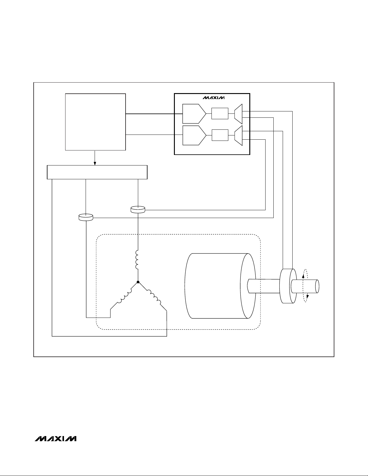
Three-Phase Motor Controller
The MAX1377/MAX1379/MAX1383 are ideally suited for
motor-control systems (Figure 16). The devices’ simultaneously sampled inputs eliminate the need for complicated DSP algorithms that realign sequentially sampled
data into a simultaneous sample set. The ±10V
(MAX1383) input allows for standard industrial inputs,
eliminating the need for voltage-scaling amplifiers.
Wireless Communication
Use the MAX1377/MAX1379/MAX1383 in a variety of
wireless communication systems. These devices allow
precise, simultaneous sampling of the I and Q signals
of quadrature RF receiver systems. Figure 17 shows the
MAX1377 in a simplified quadrature system. The device
has a differential input option that allows either full differential or psuedo-differential signals. The 2:1 input
mux allows measurement of RSSI and other systemmonitoring functions with this device.
Figure 12. Full Power-Down Mode Timing Sequence
Figure 13. Data Valid and Hold Times
CNVST
SCLK
1ST SCLK RISING EDGE
DOUT_
MODE
REF
0
0
0
NORMAL
D10 D8 D7
D11
1ST SCLK RISING EDGE
D9
EXECUTE PARTIAL POWER-DOWN SEQUENCE TWICE
DOUT_ ENTERS THREE-STATE ONCE CNVST GOES HIGH
0
ENABLED
SCLK
DOUT_
0
0
t
DOUT
PPD
000
t
DHOLD
0
0
DISABLED
FPD
Page 18

MAX1377/MAX1379/MAX1383
Dual, 12-Bit, 1.25Msps Simultaneous-Sampling
ADCs with Serial Interface
18 ______________________________________________________________________________________
Layout, Grounding, and Bypassing
For best performance, use PCBs with ground planes.
Ensure that digital and analog signal lines are separated from each other. Do not run analog and digital
(especially clock) lines parallel to one another or digital
lines underneath the ADC package.
Establish a single-point analog ground (star ground point)
at AGND, separate from the digital ground, DGND.
Connect all other analog grounds and DGND to this star
ground point for further noise reduction. The ground return
to the power supply for this ground should be low impedance and as short as possible for noise-free operation.
See Figure 14.
High-frequency noise in the AVDD power supply affects
the ADC’s high-speed comparator. Bypass the supply
to the single-point analog ground with 0.01µF and 10µF
bypass capacitors. Minimize capacitor lead lengths for
best supply-noise rejection.
Definitions
Integral Nonlinearity
Integral nonlinearity (INL) is the deviation of the values
on an actual transfer function from a straight line. This
straight line can be either a best-straight-line fit or a line
drawn between the end points of the transfer function,
once offset and gain errors have been nulled. The static
linearity parameters for the MAX1377/MAX1379/
MAX1383 are measured using the end-points method.
Differential Nonlinearity
Differential nonlinearity (DNL) is the difference between
an actual step width and the ideal value of 1 LSB. A
DNL error specification of 1 LSB or less guarantees no
missing codes and a monotonic transfer function.
Aperture Jitter
Aperture jitter (tAJ) is the sample-to-sample variation in
the time between the samples.
Aperture Delay
Aperture delay (tAD) is the time defined between the
falling edge of CNVST and the instant when an actual
sample is taken.
Figure 15. Common Serial-Interface Connections to the
MAX1377/MAX1379/MAX1383
Figure 14. Power-Supply Grounding and Bypassing
SUPPLIES
ANALOG
SUPPLY
RETURN RETURN
DIGITAL
SUPPLY
A) SPI
SCK
MISO1
MISO2
SCK
MISO1
MISO2
I/O
3V TO 5V
SS
CS
3V TO 5V
CNVST
SCLK
DOUT1
DOUT2
CNVST
SCLK
DOUT1
DOUT2
MAX1377
MAX1379
MAX1383
MAX1377
MAX1379
MAX1383
OPTIONAL
FERRITE
BEAD
AVDD
AGND DGND
MAX1377
MAX1379
MAX1383
V
L
V
DD
CIRCUITRY
DIGITAL
B) QSPI
GND
C) MICROWIRE
SS
I/O
SK
SI1
SI2
CNVST
SCLK
DOUT1
DOUT2
MAX1377
MAX1379
MAX1383
Page 19
MAX1377/MAX1379/MAX1383
Dual, 12-Bit, 1.25Msps Simultaneous-Sampling
ADCs with Serial Interface
______________________________________________________________________________________ 19
Figure 16. Three-Phase Motor Control
DSP-BASED DIGITAL
PROCESSING ENGINE
IGBT CURRENT DRIVERS
CURRENT
SENSORS
I
PHASE1
MISO1
MISO2
I
PHASE2
PHASE 2
MAX1383
12-BIT
ADC
12-BIT
ADC
THREE-PHASE ELECTRIC MOTOR
T/H
T/H
AIN1A
AIN1B
AIN2A
AIN2B
PHASE 1
= - I
I
PHASE3
PHASE1
- I
PHASE2
PHASE 3
SIN/COS
POSITION
RESOLVER
Page 20

Signal-to-Noise Ratio
For a waveform perfectly reconstructed from digital
samples, signal-to-noise ratio (SNR) is the ratio of fullscale analog input (RMS value) to the RMS quantization
error (residual error). The theoretical minimum analogto-digital noise is caused by quantization error, and
results directly from the ADC’s resolution (N bits):
SNR = (6.02 x N + 1.76)dB
In reality, there are other noise sources besides quantization noise, including thermal noise, reference noise,
clock jitter, etc. Therefore, SNR is computed by taking
the ratio of the RMS signal to the RMS noise, which
includes all spectral components minus the fundamental, the first five harmonics, and the DC offset.
Signal-to-Noise Plus Distortion
Signal-to-noise plus distortion (SINAD) is the ratio of the
fundamental input frequency’s RMS amplitude to the
RMS equivalent of all other ADC output signals:
SINAD(dB) = 20 x log(SignalRMS/NoiseRMS)
Effective Number of Bits
Effective number of bits (ENOB) indicates the global
accuracy of an ADC at a specific input frequency and
sampling rate. An ideal ADC’s error consists of quantization noise only. With an input range equal to the fullscale range of the ADC, calculate the ENOB as follows:
Total Harmonic Distortion
Total harmonic distortion (THD) is the ratio of the RMS
sum of the first five harmonics of the input signal to the
fundamental itself. This is expressed as:
where V1is the fundamental amplitude, and V2through
V
5
are the amplitudes of the 2nd- through 5th-order
harmonics.
Spurious-Free Dynamic Range
Spurious-free dynamic range (SFDR) is the ratio of the
RMS amplitude of the fundamental (maximum signal
component) to the RMS value of the next largest distortion component.
Full-Power Bandwidth
Full-power bandwidth is the frequency at which the input
signal amplitude attenuates by 3dB for a full-scale input.
Full-Linear Bandwidth
Full-linear bandwidth is the frequency at which the signal-to-noise plus distortion (SINAD) is equal to 56dB.
Intermodulation Distortion
Any device with nonlinearities creates distortion products when two sine waves at two different frequencies
(f1 and f2) are input into the device. Intermodulation
distortion (IMD) is the total power of the IM2 to IM5
intermodulation products to the Nyquist frequency relative to the total input power of the two input tones, f1
and f2. The individual input tone levels are at
-6dBFS.
Chip Information
PROCESS: BiCMOS
MAX1377/MAX1379/MAX1383
Dual, 12-Bit, 1.25Msps Simultaneous-Sampling
ADCs with Serial Interface
20 ______________________________________________________________________________________
Figure 17. Quadrature Wireless-Communication System
V
AVDD
L
T/R
QUADRATURE
DEMODULATOR
QUADRATURE
TRANSMITTER
V
MAX1377
I
Q
12-BIT
ADC
12-BIT
ADC
DAC
DAC
L
DSP
PROCESSING
THD
log
=×
20
⎛
2
2
VVVV
+++
2
⎜
⎜
⎝
3
2
4
V
1
⎞
2
5
⎟
⎟
⎠
SINAD=−
ENOB
⎛
⎜
⎝
176
⎞
⎟
602..
⎠
Page 21

MAX1377/MAX1379/MAX1383
Dual, 12-Bit, 1.25Msps Simultaneous-Sampling
ADCs with Serial Interface
______________________________________________________________________________________ 21
Functional Diagram
Selector Guide
AIN1A
AIN1B
REF
REFSEL
RGND
MUX
T/H
A = 1
AVDD
INTERNAL
REFERENCE
12-BIT
SAR
ADC1
V
L
OUTPUT
BUFFER
SERIAL
INTERFACE
AND TIMING
CONTROL
LOGIC
DOUT1
CS
CNVST
SCLK
U/B
S/D
V
OUTPUT
BUFFER
L
DOUT2
AIN2A
AIN2B
MUX
SEL
T/H
AGND
12-BIT
SAR
ADC2
MAX1377
MAX1379
MAX1383
DGND
INTERNAL
PART SUPPLY VOLTAGE (V)
REFERENCE
VOLTAGE (V)
MAX1377 2.7 to 3.6 2.048 0 to V
MAX1379 4.75 to 5.25 4.096 0 to V
MAX1383 4.75 to 5.25 2.5 ±10V 1.25
INPUT VOLTAGE
RANGE
REF, ±VREF
REF, ±VREF
SAMPLING RATE
(Msps)
/2 1.25
/2 1.25
Page 22

MAX1377/MAX1379/MAX1383
Dual, 12-Bit, 1.25Msps Simultaneous-Sampling
ADCs with Serial Interface
Maxim cannot assume responsibility for use of any circuitry other than circuitry entirely embodied in a Maxim product. No circuit patent licenses are
implied. Maxim reserves the right to change the circuitry and specifications without notice at any time.
22
____________________Maxim Integrated Products, 120 San Gabriel Drive, Sunnyvale, CA 94086 408-737-7600
© 2008 Maxim Integrated Products is a registered trademark of Maxim Integrated Products, Inc.
PACKAGE TYPE PACKAGE CODE DOCUMENT NO.
20 TQFN-EP T2055-4
21-0140
Package Information
For the latest package outline information and land patterns, go to www.maxim-ic.com/packages.
 Loading...