

Page 1
General Description
The MAX1365/MAX1367 low-power, 4.5- and 3.5-digit,
panel meters feature an integrated sigma-delta analogto-digital converter (ADC), LED display drivers, voltage
digital-to-analog converter (DAC), and a 4–20mA
(or 0 to 16mA) current driver.
The MAX1365/MAX1367’s analog input voltage range is
programmable to either ±2V or ±200mV. The MAX1367
drives a 3.5-digit (±1999 count) display and the
MAX1365 drives a 4.5-digit (±19,999 count) display.
The ADC output directly drives the LED display as well
as the voltage DAC, which in turn drives the 4–20mA
(or 0 to 16mA) current-loop output.
In normal operation, the 0 to 16mA/4–20mA currentloop output follows the ±2V or ±200mV analog input to
drive remote panel-meter displays, data loggers, and
other industrial controllers. For added flexibility, the
MAX1365/MAX1367 allow direct access to the DAC
output and the V/I converter input.
The sigma-delta ADC does not require external precision integrating capacitors, autozero capacitors, crystal
oscillators, charge pumps, or other circuitry commonly
required in dual-slope ADC panel-meter circuits. Onchip analog input and reference buffers allow direct
interface with high-impedance signal sources. Excellent
common-mode rejection and digital filtering provide
greater than 100dB rejection of simultaneous 50Hz and
60Hz line noise. Other features include data hold, peak
detection, and overrange/underrange detection.
The MAX1365/MAX1367 require a 2.7V to 5.25V supply,
a 4.75V to 5.25V V/I supply, and a 7V to 30V loop supply. They are available in a space-saving (7mm x
7mm), 48-pin TQFP package and operate over the
extended (-40°C to +85°C) temperature range.
Applications
Automated Test Equipment
Data-Acquisition Systems
Digital Multimeters
Digital Panel Meters
Digital Voltmeters
Industrial Process Control
Features
♦ Stand-Alone, Digital Panel Meter
20-Bit Sigma-Delta ADC
4.5-Digit Resolution (±19,999 Count, MAX1365)
3.5-Digit Resolution (±1999 Count, MAX1367)
No Integrating/Autozeroing Capacitors
100MΩ Input Impedance
±200mV or ±2.000V Input Range
♦ LED Display
Common-Cathode 7-Segment LED Driver
Programmable LED Current (0 to 20mA)
2.5Hz Update Rate
♦ Output DAC and Current Driver
±15-Bit DAC with 14-Bit Linear V/I Converter
Selectable 0 to 16mA or 4–20mA Current Output
Unipolar/Bipolar Modes
±50µA Zero Scale, ±40ppmFS/°C (typ)
±0.5% Gain Error, ±25ppmFS/°C (typ)
Separate 7V to 30V Supply for Current-Loop
Output
♦ 2.7V to 5.25V ADC/DAC Supply
♦ 4.75V to 5.25V V/I Converter Supply
♦ Internal 2.048V Reference or External Reference
♦ 48-Pin, 7mm x 7mm TQFP Package
MAX1365/MAX1367
Stand-Alone, 4.5-/3.5-Digit Panel Meters
with 4–20mA Output
________________________________________________________________ Maxim Integrated Products 1
Selector Guide
19-3889; Rev 1; 1/06
For pricing, delivery, and ordering information, please contact Maxim/Dallas Direct! at
1-888-629-4642, or visit Maxim’s website at www.maxim-ic.com.
PART TEMP RANGE
PIN-PACKAGE
MAX1365ECM -40°C to +85°C 48 TQFP
MAX1367ECM -40°C to +85°C 48 TQFP
Ordering Information
PART
RESOLUTION
(DIGITS)
PKG
CODE
MAX1365ECM 4.5 C48-6
MAX1367ECM 3.5 C48-6
Pin Configuration appears at end of datasheet.
Typical Operating Circuits appear at end of datasheet.
Page 2
MAX1365/MAX1367
Stand-Alone, 4.5-/3.5-Digit Panel Meters
with 4–20mA Output
2 _______________________________________________________________________________________
ABSOLUTE MAXIMUM RATINGS
ELECTRICAL CHARACTERISTICS
(AVDD= DVDD= DAC_VDD = +2.7V to +5.25V, GND = 0, V
LEDV
= +2.7V to +5.25V, LEDG = 0, V
REF+
- V
REF-
= 2.048V (external
reference), 4-20OUT = 7V, V
REG_AMP
= +5.0V, C
REF+
= 0.1µF, REF- = GND, C
NEGV
= 0.1µF. Internal clock mode, unless otherwise
noted. All specifications are at T
A
= T
MIN
to T
MAX
. Typical values are at TA = +25°C, unless otherwise noted.)
Stresses beyond those listed under “Absolute Maximum Ratings” may cause permanent damage to the device. These are stress ratings only, and functional
operation of the device at these or any other conditions beyond those indicated in the operational sections of the specifications is not implied. Exposure to
absolute maximum rating conditions for extended periods may affect device reliability.
AV
DD, DVDD ....................................................................
-0.3V to +6.0V
AIN+, AIN-, REF+, REF-.........................V
NEGV
to (AVDD+ 0.3V)
REG_FORCE, CMP, DAC_VDD, DACVOUT,
CONV_IN, 4-20OUT.............................-0.3V to (AV
DD
+ 0.3V)
EN_BPM, EN_I, REFSELE, DACDATA_SEL, INTREF, RANGE,
DPSET1, DPSET2, HOLD, PEAK, DPON,
CS_DAC...............................................-0.3V to (DV
DD
+ 0.3V)
NEGV .......................................................-2.6V to (AV
DD
+ 0.3V)
LED_EN....................................................-0.3V to (DV
DD
+ 0.3V)
SET...........................................................-0.3V to (AV
DD
+ 0.3V)
REG_AMP, REG_VDD ...........................................-0.3V to +6.0V
LEDV......................................................................-0.3V to +6.0V
LEDG .....................................................................-0.3V to +0.3V
GND_DAC .............................................................-0.3V to +0.3V
GND_V/I.................................................................-0.3V to +0.3V
SEG_ to LEDG.........................................-0.3V to (V
LEDV
+ 0.3V)
DIG_ to LEDG..........................................-0.3V to (V
LEDV
+ 0.3V)
REF_DAC .................................................-0.3V to (AV
DD
+ 0.3V)
DIG_ Sink Current .............................................................300mA
DIG_ Source Current...........................................................50mA
SEG_ Sink Current . ............................................................50mA
SEG_ Source Current..........................................................50mA
Maximum Current Input into Any Other Pin . ......................50mA
Continuous Power Dissipation (T
A
= +70°C)
48-Pin TQFP (derate 22.7mW/°C above +70°C).....1818.2mW
Operating Temperature Range ...........................-40°C to +85°C
Storage Temperature Range .............................-60°C to +150°C
Junction Temperature......................................................+150°C
Lead Temperature (soldering, 10s) .................................+300°C
PARAMETER
CONDITIONS
UNITS
ADC ACCURACY
MAX1365
Noise-Free Resolution
MAX1367
Counts
2.000V range ±1
Integral Nonlinearity (Note 1) INL
200mV range ±1
Counts
Range Change Ratio
(V
AIN+
- V
AIN-
= 0.100V) on 200mV range;
(V
AIN+
- V
AIN-
= 0.100V) on 2.0V range
Ratio
Rollover Error V
AIN+
- V
AIN-
= full scale ±1
Counts
Output Noise 10
µV
P-P
Offset Error (Zero Input Reading)
V
AIN+
- V
AIN-
= 0 (Note 2) -0 +0
Counts
Gain Error (Note 3) -0.5
%FSR
Offset Drift (Zero Reading Drift) V
AIN+
- V
AIN-
= 0 (Note 4) 0.1
µV/°C
Gain Drift ±1
ppm/°C
INPUT CONVERSION RATE
Update Rate 5Hz
ANALOG INPUTS (AIN+, AIN-) (bypass to GND with 0.1µF or greater capacitors)
RANGE = GND -2.0
AIN Input Voltage Range (Note 5)
RANGE = DV
DD
-0.2
V
AIN Absolute Input Voltage
Range to GND
-2.2
V
Normal-Mode 50Hz and 60Hz
Rejection (Simultaneously)
50Hz and 60Hz ±2% 100 dB
SYMBOL
MIN TYP MAX
-19,999 +19,999
-1999 +1999
10:1
+0.5
+2.0
+0.2
+2.2
Page 3
MAX1365/MAX1367
Stand-Alone, 4.5-/3.5-Digit Panel Meters
with 4–20mA Output
_______________________________________________________________________________________ 3
PARAMETER
SYMBOL
CONDITIONS
MIN
TYP
MAX
UNITS
Common-Mode 50Hz and 60Hz
Rejection (Simultaneously)
CMR
For 50Hz and 60Hz ±2%, R
SOURCE
<
10kΩ
150 dB
Common-Mode Rejection CMR At DC 100 dB
Input Leakage Current 10 nA
Input Capacitance 10 pF
Average Dynamic Input Current -20
nA
INTERNAL REFERENCE (REF- = GND, INTREF = DVDD)
REF Input Voltage V
REF
V
REF Output Short-Circuit Current
1mA
REF Output Temperature
Coefficient
40
ppm/°C
Load Regulation I
SOURCE
= 0 to 300µA, I
SINK
= 0 to 30µA 6
µV/µA
Line Regulation 50 µV/V
0.1Hz to 10Hz 25
Noise Voltage
10Hz to 10kHz 400
µV
P-P
EXTERNAL REFERENCE (INTREF = GND)
REF Input Voltage Differential (V
REF+
- V
REF-
)
V
Absolute REF+, REF- Input
Voltage to GND (V
REF+
Must Be
Greater Than V
REF-
)
-2.2
V
Normal-Mode 50Hz and 60Hz
Rejection (Simultaneously)
50Hz and 60Hz ±2% 100 dB
Common-Mode 50Hz and 60Hz
Rejection (Simultaneously)
CMR
For 50Hz and 60Hz ±2%, R
SOURCE
<
10kΩ
150 dB
Common-Mode Rejection CMR At DC 100 dB
Input Leakage Current 10 nA
Input Capacitance 10 pF
Average Dynamic Input Current (Note 6) -20
nA
CHARGE PUMP
Output Voltage NEGV C
NEGV
= 0.1µF to GND
V
DIGITAL INPUTS (INTREF, RANGE, PEAK, HOLD, DPSET1, DPSET2)
Input Current I
IN
VIN = 0 or DV
DD
-10
µA
Input Low Voltage V
INL
0.3 x
V
Input High Voltage V
INH
0.7 x
V
Input Hysteresis V
HYS
DV
DD
= 3V 200 mV
ELECTRICAL CHARACTERISTICS (continued)
(AVDD= DVDD= DAC_VDD = +2.7V to +5.25V, GND = 0, V
LEDV
= +2.7V to +5.25V, LEDG = 0, V
REF+
- V
REF-
= 2.048V (external
reference), 4-20OUT = 7V, V
REG_AMP
= +5.0V, C
REF+
= 0.1µF, REF- = GND, C
NEGV
= 0.1µF. Internal clock mode, unless otherwise
noted. All specifications are at T
A
= T
MIN
to T
MAX
. Typical values are at TA = +25°C, unless otherwise noted.)
TC
VREF
2.007 2.048 2.089
-2.60 -2.42 -2.30
DV
2.048
DD
+20
+2.2
+20
+10
DV
DD
Page 4
MAX1365/MAX1367
Stand-Alone, 4.5-/3.5-Digit Panel Meters
with 4–20mA Output
4 _______________________________________________________________________________________
ELECTRICAL CHARACTERISTICS (continued)
(AVDD= DVDD= DAC_VDD = +2.7V to +5.25V, GND = 0, V
LEDV
= +2.7V to +5.25V, LEDG = 0, V
REF+
- V
REF-
= 2.048V (external
reference), 4-20OUT = 7V, V
REG_AMP
= +5.0V, C
REF+
= 0.1µF, REF- = GND, C
NEGV
= 0.1µF. Internal clock mode, unless otherwise
noted. All specifications are at T
A
= T
MIN
to T
MAX
. Typical values are at TA = +25°C, unless otherwise noted.)
PARAMETER
CONDITIONS
ADC POWER SUPPLY (Note 7)
AVDD Voltage AV
DD
V
DVDD Voltage DV
DD
V
Power-Supply Rejection AV
DD
PSR
A
(Note 8) 80 dB
Power-Supply Rejection DV
DD
PSR
D
(Note 8) 100 dB
AV
DD
Current (Note 9) I
AVDD
Standby mode
µA
DVDD = +5.25V
DVDD = +3.3V
DV
DD
Current (Note 9) I
DVDD
Standby mode 20
µA
DAC POWER SUPPLY
DAC Supply Voltage
V
DAC Supply Current
mA
LINEAR REGULATOR AND V/I CONVERTER POWER REQUIREMENTS
REG_AMP Supply Voltage
V
REG_AMP Supply Current
mA
REG_VDD Supply Voltage
V
REG_VDD Supply Current Includes 20mA programmed current
mA
LED DRIVERS
LED Supply Voltage V
LEDV
V
LED Shutdown Supply Current I
SHDN
10 µA
LED Supply Current I
LEDV
176
mA
MAX1365 512
Display Scan Rate f
OSC
MAX1367 640
Hz
Segment Current Slew Rate I
SEG
/∆t25
DIG_ Voltage Low V
DIG
V
Segment-Drive Source-Current
Matching
∆I
SEG
3
%
Segment-Drive Source Current I
SEG
V
LEDV
- V
SEG
= 0.6V, R
SET
= 25kΩ
mA
LED Drivers Bias Current From AV
DD
120 µA
Interdigit Blanking Time 4µs
SYMBOL
MIN TYP MAX UNITS
2.70 5.25
2.70 5.25
640
305
320
180
V
V
V
DAC_VDD
REG_AMP
REG_VDD
2.70 5.25
0.10 0.21
4.75 5.25
0.19 0.30
5.20
25.2 27.4
2.70 5.25
180
0.178 0.300
±12
15.0 21.5 25.5
mA/µs
Page 5
MAX1365/MAX1367
Stand-Alone, 4.5-/3.5-Digit Panel Meters
with 4–20mA Output
_______________________________________________________________________________________ 5
ELECTRICAL CHARACTERISTICS (continued)
(AVDD= DVDD= DAC_VDD = +2.7V to +5.25V, GND = 0, V
LEDV
= +2.7V to +5.25V, LEDG = 0, V
REF+
- V
REF-
= 2.048V (external
reference), 4-20OUT = 7V, V
REG_AMP
= +5.0V, C
REF+
= 0.1µF, REF- = GND, C
NEGV
= 0.1µF. Internal clock mode, unless otherwise
noted. All specifications are at T
A
= T
MIN
to T
MAX
. Typical values are at TA = +25°C, unless otherwise noted.)
PARAMETER
SYMBOL
CONDITIONS
MIN
TYP
MAX
UNITS
DAC OUTPUT ACCURACY
Zero-Scale Error 4–20mA or 0 to 16mA mode, TA = +25°C
µA
Zero-Scale Error Tempco ±40
Gain Error 4–20mA or 0 to 16mA mode, TA = +25°C
%FS
Gain-Error Tempco ±25
Span Linearity ±2 ±4µA
Power-Supply Rejection PSR V
EXT
= 7V to 30V 4 µA/V
Signal Path Noise 10pF to GND on 4-20OUT 2.0
4–20mA Current Limit Limited to 12.5 x V
REF
/ 1.28kΩ 20 mA
Note 1: Integral nonlinearity is the deviation of the analog value at any code from its theoretical value after nulling the gain error and
offset error.
Note 2: Offset calibrated.
Note 3: Offset nulled.
Note 4: Drift error is eliminated by recalibration at the new temperature.
Note 5: The input voltage range for the analog inputs is given with respect to the voltage on the negative input of the differential pair.
Note 6: V
AIN+
or V
AIN-
= -2.2V to +2.2V. V
REF+
or V
REF-
= -2.2V to +2.2V. All input structures are identical. Production tested on
AIN+ and REF+ only. V
REF+
must always be greater than V
REF-
.
Note 7: Power-supply currents are measured with all digital inputs at either GND or DV
DD
.
Note 8: Measured at DC by changing the power-supply voltage from 2.7V to 5.25V and measuring the effect on the conversion error
with external reference. PSRR at 50Hz and 60Hz exceeds 120dB with filter notches at 50Hz and 60Hz (Figure 1).
Note 9: LED drivers are disabled.
±50
±0.5
p p mFS /° C
p p mFS /° C
µA
RMS
Page 6
MAX1365/MAX1367
Stand-Alone, 4.5-/3.5-Digit Panel Meters
with 4–20mA Output
6 _______________________________________________________________________________________
0
300
200
100
400
500
600
700
800
900
1000
2.7 3.73.2 4.2 4.7 5.2
SUPPLY CURRENT
vs. SUPPLY VOLTAGE
MAX1365/67 toc01
SUPPLY VOLTAGE (V)
SUPPLY CURRENT (µA)
DAC_VDD
AV
DD
DV
DD
0
200
100
400
300
600
500
700
-40 10-15 35 60 85
SUPPLY CURRENT vs. TEMPERATURE
MAX1365/67 toc02
TEMPERATURE (°C)
SUPPLY CURRENT (µA)
AV
DD
DV
DD
DAC_VDD
MAX1365
OFFSET ERROR vs. SUPPLY VOLTAGE
MAX1365/67 toc03
SUPPLY VOLTAGE (V)
OFFSET ERROR (LSB)
4.754.253.753.25
-0.11
-0.06
-0.01
0.04
0.09
0.14
0.19
-0.16
2.75 5.25
MAX1365
OFFSET ERROR vs. TEMPERATURE
MAX1365/67 toc04
TEMPERATURE (°C)
OFFSET ERROR (LSB)
605010 20 30 40
-0.1
0
0.1
0.2
0.3
0.4
0.5
0.6
-0.2
070
MAX1365
GAIN ERROR vs. SUPPLY VOLTAGE
MAX1365/67 toc05
SUPPLY VOLTAGE (V)
GAIN ERROR (% FULL SCALE)
4.754.253.25 3.75
-0.08
-0.04
-0.06
-0.02
0
0.02
0.04
0.06
0.08
-0.10
2.75 5.25
MAX1365
GAIN ERROR vs. TEMPERATURE
MAX1365/67 toc06
TEMPERATURE (°C)
GAIN ERROR (% FULL SCALE)
605030 402010
-0.09
-0.08
-0.07
-0.06
-0.05
-0.04
-0.03
-0.02
-0.01
0
-0.10
070
MAX1365
INL (±200mV INPUT RANGE) vs. OUTPUT CODE
MAX1365/67 toc07
OUTPUT CODE
INL (COUNTS)
10,0000-10,000
-0.5
0
0.5
1.0
-1.0
-20,000 20,000
MAX1365
INL (±2V INPUT RANGE) vs. OUTPUT CODE
MAX1365/67 toc08
OUTPUT CODE
INL (COUNTS)
10,0000-10,000
-0.5
0
0.5
1.0
-1.0
-20,000 20,000
NOISE DISTRIBUTION
MAX1365/67 toc09
NOISE (LSB)
PERCENTAGE OF UNITS (%)
0.80.70.60.50.40.30.20.10-0.1
5
10
15
20
25
0
-0.2
Typical Operating Characteristics
(A
VDD
= D
VDD
= +5V, V
DAC_VDD
= +5.0V, GND = 0, LEDG = 0, V
LEDV
= +2.7V to +5.25V, V
REF+
- V
REF-
= 2.048V (external refer-
ence), V
EXT
= 7V, C
REF+
= C
REF-
= 0.1µF, C
NEGV
= 0.1µF. Internal clock mode, unless otherwise noted. TA= +25°C, unless other-
wise noted.)
Page 7
MAX1365/MAX1367
Stand-Alone, 4.5-/3.5-Digit Panel Meters
with 4–20mA Output
_______________________________________________________________________________________ 7
INTERNAL REFERENCE VOLTAGE
vs. TEMPERATURE
MAX1365/67 toc10
TEMPERATURE (°C)
REFERENCE VOLTAGE (V)
605040302010
2.046
2.045
2.047
2.049
2.048
2.051
2.050
2.053
2.052
2.054
2.044
070
INTERNAL REFERENCE VOLTAGE
vs. ANALOG SUPPLY VOLTAGE
MAX1365/67 toc11
SUPPLY VOLTAGE (V)
REFERENCE VOLTAGE (V)
4.754.253.753.25
2.045
2.046
2.047
2.048
2.049
2.050
2.044
2.75 5.25
DATA OUTPUT RATE
vs. TEMPERATURE
MAX1365/67 toc12
TEMPERATURE (°C)
DATA OUTPUT RATE (Hz)
6035-15 10
4.92
4.98
4.96
4.94
5.00
5.02
5.04
5.06
5.08
5.10
4.90
-40 85
DATA OUTPUT RATE
vs. SUPPLY VOLTAGE
MAX1365/67 toc13
SUPPLY VOLTAGE (V)
DATA OUTPUT RATE (Hz)
4.744.233.21 3.72
4.995
4.990
4.985
5.000
5.005
5.010
5.015
5.020
4.980
2.70 5.25
OFFSET ERROR
vs. COMMON-MODE VOLTAGE
MAX1365/67 toc14
COMMON-MODE VOLTAGE (V)
OFFSET ERROR (LSB)
1.51.0-1.5 -1.0 -0.5 0 0.5
-0.15
-0.10
-0.05
0
0.05
0.10
0.15
0.20
-0.20
-2.0 2.0
V
NEG
STARTUP SCOPE SHOT
MAX1365/67 toc15
20ms/div
2V/div
1V/div
V
DD
V
NEG
CHARGE-PUMP OUTPUT VOLTAGE
vs. ANALOG SUPPLY VOLTAGE
MAX1365/67 toc16
SUPPLY VOLTAGE (V)
V
NEG
VOLTAGE (V)
4.754.253.753.25
-2.48
-2.46
-2.44
-2.42
-2.40
-2.50
2.75 5.25
SEGMENT CURRENT
vs. SUPPLY VOLTAGE
MAX1365/67 toc17
SUPPLY VOLTAGE (V)
SEGMENT CURRENT (µA)
4.744.233.723.21
5
10
15
20
25
30
0
2.70 5.25
R
ISET
= 25kΩ
-0.2
0
-0.1
0.2
0.1
0.3
0.4
-40 10-15 35 60 85
DAC ZERO-CODE OFFSET ERROR
vs. TEMPERATURE
MAX1365/67 toc18
TEMPERATURE (°C)
OFFSET ERROR (LSB)
Typical Operating Characteristics (continued)
(A
VDD
= D
VDD
= +5V, V
DAC_VDD
= +5.0V, GND = 0, LEDG = 0, V
LEDV
= +2.7V to +5.25V, V
REF+
- V
REF-
= 2.048V (external refer-
ence), V
EXT
= 7V, C
REF+
= C
REF-
= 0.1µF, C
NEGV
= 0.1µF. Internal clock mode, unless otherwise noted. TA= +25°C, unless other-
wise noted.)
Page 8
Stand-Alone, 4.5-/3.5-Digit Panel Meters
with 4–20mA Output
8 _______________________________________________________________________________________
Typical Operating Characteristics (continued)
(A
VDD
= D
VDD
= +5V, V
DAC_VDD
= +5.0V, GND = 0, LEDG = 0, V
LEDV
= +2.7V to +5.25V, V
REF+
- V
REF-
= 2.048V (external refer-
ence), V
EXT
= 7V, C
REF+
= C
REF-
= 0.1µF, C
NEGV
= 0.1µF. Internal clock mode, unless otherwise noted. TA= +25°C, unless other-
wise noted.)
-0.30
-0.20
-0.25
-0.10
-0.15
-0.05
0
-40 10-15 35 60 85
DAC GAIN ERROR
vs. TEMPERATURE
MAX1365/67 toc19
TEMPERATURE (°C)
GAIN ERROR (LSB)
4–20OUT
= 21.7mA
CONV_IN
= 1V
10mA/div
500mV/div
STEP RESPONSE
MAX1365/67 toc20
100µs/div
-50
-20
-30
-40
0
-10
40
30
20
10
50
-40 -20 0 20 40 60 80
4–20OUT ZERO-SCALE ERROR
vs. TEMPERATURE
MAX1365/67 toc21
TEMPERATURE (°C)
CURRENT OUTPUT (µA)
EXTERNAL REFERENCE = 2.048V
-50
-20
-30
-40
0
-10
40
30
20
10
50
-40 -20 0 20 40 60 80
4–20OUT GAIN ERROR
vs. TEMPERATURE
MAX1365/67 toc22
TEMPERATURE (°C)
GAIN ERROR (%)
EXTERNAL REFERENCE = 2.048V
4–20mA MODE
0 TO 16mA MODE
-0.5
0
0.5
1.0
1.5
2.0
2.5
-20,000 -10,000 0 10,000 20,000
4–20OUT vs. DAC CODE
(4–20OUT SPAN LINEARITY)
MAX1365/67 toc24
DAC CODE (COUNTS)
SPAN LINEARITY (µA)
OFFSET ENABLED
(EN_I = HIGH)
-150
-100
-50
0
50
100
150
486101214161820
POWER-SUPPLY REJECTION
vs. CURRENT OUTPUT (4-20OUT)
MAX1365/67 toc23
4-20OUT OUTPUT CURRENT (mA)
POWER-SUPPLY REJECTION (nA/V)
Page 9

MAX1365/MAX1367
Stand-Alone, 4.5-/3.5-Digit Panel Meters
with 4–20mA Output
_______________________________________________________________________________________ 9
PIN NAME FUNCTION
1 AIN+
Positive Analog Input. Positive side of fully differential analog input. Bypass AIN+ to GND with a
0.1µF or greater capacitor.
2 AIN-
Negative Analog Input. Negative side of fully differential analog input. Bypass AIN- to GND with a
0.1µF or greater capacitor.
3 GND Ground. Connect to star ground.
4AV
DD
Analog Positive Supply Voltage. Connect AVDD to a +2.7V to +5.25V power supply. Bypass AV
DD
to GND with a 0.1µF capacitor.
5DV
DD
Digital Positive Supply Voltage. Connect DVDD to a +2.7V to +5.25V power supply. Bypass DV
DD
to GND with a 0.1µF capacitor.
6 SET
Segment Current Set. Connect to ground through a resistor to set the segment current. See Table
7 for segment-current selection.
7 REG_VDD V/I Converter Regulated Supply Output (5.2V typ)
8
REG_VDD Control. Drives the gate of external depletion-mode FET.
9 REG_AMP Regulator/Reference Buffer Supply. Connect to a 4.75V to 5.25V power supply.
10 CMP Regulator Compensation Node. Connect a 0.1µF capacitor from CMP to REG_FORCE.
11 DAC_VDD DAC Analog Supply. Connect DAC_VDD to a +2.7V to +5.25V power supply.
12 DACVOUT DAC Voltage Output. DAC output impedance is typically 6.2kΩ.
13 CONV_IN V/I Converter Input
14 4-20OUT 4–20mA (0 to 16mA) Current-Loop Output. Referenced to GND.
15 GND_DAC DAC Analog Ground. Connect to star ground.
16 GND_V/I V/I Converter Analog Ground. Connect to star ground.
17 REF_DAC
V-to-I Converter/DAC Reference Input. Connect a voltage source for external reference operation
or leave floating for internal reference. Bypass REF_DAC with a 0.1µF capacitor to GND for either
internal or external reference operation.
18 EN_BPM Acti ve- H i g h V /I- C onver ter Bi p ol ar - M od e E nab l e. S et hi g h for b i p ol ar m od e. S et l ow for uni p ol ar m od e.
19 EN_I
Acti ve- H i g h V /I- C onver ter 4m A O ffset E nab l e. S et l ow for 0 to 16m A outp ut. S et hi g h for 4–20m A.
20 REFSELE
DAC External Reference Selection. Set low for internal reference. Set high for external reference.
Leave REF_DAC unconnected when REFSELE is low.
21
DAC Data-Source Select. Connect to logic high for the MAX1365/MAX1367.
22 CS_DAC DAC Chip Select. Connect to logic high for the MAX1365/MAX1367.
23 INTREF
ADC Reference Selection. Set INTREF high to select the internal ADC reference. Set INTREF low
to select external ADC reference.
24 RANGE
ADC Range Select. Set RANGE low for ±2V analog input voltage range. Set RANGE high for
±200mV analog input voltage range.
25 PEAK
Peak Logic Input. Connect PEAK to DV
DD
to display the highest ADC value on the LED. Connect
PEAK to GND to disable the PEAK function (see Table 1).
Pin Description
REG_FORCE
DACDATA_SEL
Page 10

MAX1365/MAX1367
Stand-Alone, 4.5-/3.5-Digit Panel Meters
with 4–20mA Output
10 ______________________________________________________________________________________
PIN NAME FUNCTION
26 HOLD
Hold Logic Input. Connect HOLD to DV
DD
to hold the current ADC value on the LED. Connect
HOLD to GND to update the LED at a rate of 2.5Hz and disable the hold function. Placing the
device into hold mode initiates an offset mismatch calibration. Assert HOLD high for a minimum of
2s to ensure the completion of offset mismatch calibration (see Table 1).
27 DPSET2
Display Decimal-Point Logic-Input 2. Controls the decimal point of the LED. See the Decimal-Point
Control section.
28 DPSET1
Display Decimal-Point Logic-Input 1. Controls the decimal point of the LED. See the Decimal-Point
Control section.
29 LEDG LED Segment-Drivers Ground
30 DIG0 Digit 0 Driver Out (Connected to GLED for the MAX1367)
31 DIG1 Digit 1 Driver Out
32 DIG2 Digit 2 Driver Out
33 DIG3 Digit 3 Driver Out
34 DIG4 Digit 4 Driver Out
35 SEGA Segment A Driver
36 SEGB Segment B Driver
37 LEDV
LED-Display Segment-Driver Supply. Connect to a +2.7V to +5.25V supply. Bypass with a 0.1µF
capacitor to LEDG.
38 SEGC Segment C Driver
39 SEGD Segment D Driver
40 SEGE Segment E Driver
41 SEGF Segment F Driver
42 SEGG Segment G Driver
43 SEGDP Segment DP Driver
44 LED_EN
Active-High LED Enable. The MAX1365/MAX1367 display driver turns off when LED_EN is low.
The MAX1365/MAX1367 LED-display driver turns on when LED_EN is high.
45 NEGV -2.5V Charge-Pump Voltage Output. Connect a 0.1µF capacitor to GND.
46 DPON
Decimal-Point Enable Input. Controls the decimal point of the LED. See the Decimal-Point Control
section. Connect DPON to DV
DD
to enable the decimal point.
47 REF-
ADC Negative Reference Voltage Input. For internal reference operation, connect REF- to GND.
For external reference operation, bypass REF- to GND with a 0.1µF capacitor and
set V
REF-
from -2.2V to +2.2V (V
REF+
> V
REF-
).
48 REF+
ADC Positive Reference Voltage Input. For internal reference operation, connect a 4.7µF capacitor
from REF+ to GND. For external reference operation, bypass REF+ to GND with a 0.1µF capacitor
and set V
REF+
from -2.2V to +2.2V (V
REF+
> V
REF-
).
Pin Description (continued)
Page 11

Detailed Description
The MAX1365/MAX1367 low-power, highly integrated
ADCs with LED drivers convert a ±2V differential input
voltage (one count is equal to 100µV for the MAX1365
and 1mV for the MAX1367) with a sigma-delta ADC and
output the result to an LED display. An additional
±200mV input range (one count is equal to 10µV for the
MAX1365 and 100µV for the MAX1367) is available to
measure small signals with finer resolution.
In addition to displaying the results on an LED display,
these devices feature a DAC and V-to-I converter for
4–20mA (or 0 to 16mA) current output that proportionally follows the ADC input. The MAX1365/MAX1367 use
an external depletion-mode NMOS transistor to regulate
7V to 30V for the V/I converter. Use the 4–20mA (or 0 to
16mA) output to drive a remote display, data logger,
PLC input, or other 4–20mA devices in a current loop.
The MAX1365/MAX1367 include a 2.048V reference,
internal charge pump, and a high-accuracy on-chip
oscillator. The devices feature on-chip buffers for the differential input signal and external-reference inputs,
allowing direct interface with high-impedance signal
sources. In addition, they use continuous internal offsetcalibration and offer > 100dB of 50Hz and 60Hz linenoise rejection. Other features include data hold and
peak detection and overrange/underrange detection.
Analog Input Protection
The MAX1365/MAX1367 provide internal protection
diodes that limit the analog input range on AIN+, AIN-,
REF+, and REF- from NEGV to (AVDD+ 0.3V). If the
analog input exceeds this range, limit the input current
to 10mA.
Internal Analog Input/Reference Buffers
The MAX1365/MAX1367 analog input/reference buffers
allow the use of high-impedance signal sources. The
input buffers’ common-mode input range allows the analog inputs and the reference to range from -2.2V to +2.2V.
Modulator
The MAX1365/MAX1367 perform analog-to-digital conversions using a single-bit, 3rd-order, sigma-delta modulator. The sigma-delta modulator converts the input
MAX1365/MAX1367
Stand-Alone, 4.5-/3.5-Digit Panel Meters
with 4–20mA Output
______________________________________________________________________________________ 11
LED
DRIVER
LEDG
SEGA
SEGG
DIG0(1)
DIG4(4)
LED_EN
MAX1365
MAX1367
ADC
INPUT
BUFFER
-2.5V
AIN+
AIN-
REF+
REF-
NEGV
+2.5V
2.048V
BANDGAP
REFERENCE
LOGIC
GND
CHARGE
PUMP
-2.5V
OUTPUT
DAC
DAC REF
BUFFER
AVDDDV
DD
RANGEINTREF
5V REGULATOR
V/I
CONVERTER
CURRENT
SUMMER
AND
AMPLIFIER
OFFSET
GENERATOR
EN_BPM
EN_I
DACVOUT
4-20OUT
REG_FORCE
DACDATA_SEL SETCS_DAC
REFSELE REG_AMPREF_DAC
CONV_IN
CMP REG_VDD
DAC_VDD
LEDVDPON DPSET1 DPSET 2PEAK HOLD
Functional Diagram
Page 12

MAX1365/MAX1367
Stand-Alone, 4.5-/3.5-Digit Panel Meters
with 4–20mA Output
12 ______________________________________________________________________________________
signal into a digital pulse train whose average duty
cycle represents the digitized signal information. The
modulator quantizes the input signal at a much higher
sample rate than the bandwidth of the input. The
MAX1365/MAX1367 modulator provides 3rd-order frequency shaping of the quantization noise resulting from
the single-bit quantizer. The modulator is fully differential for maximum signal-to-noise ratio and minimum susceptibility to power-supply noise. A single-bit data
stream is then presented to the digital filter to remove
the frequency-shaped quantization noise.
Digital Filtering
The MAX1365/MAX1367 contain an on-chip digital lowpass filter that processes the data stream from the
modulator using a SINC4response:
The SINC4filter has a settling time of four output data
periods (4 x 200ms). The MAX1365/MAX1367 have
25% overrange capability built into the modulator and
digital filter. The digital filter is optimized for the f
CLK
equal to 4.9152MHz. The frequency response of the
SINC4filter is calculated as follows:
where N is the oversampling ratio, and fm= N x output
data rate = 5Hz.
Filter Characteristics
Figure 1 shows the filter frequency response. The
SINC4characteristic -3dB cutoff frequency is 0.228
times the first notch frequency (5Hz). The oversampling
ratio (OSR) for the MAX1367 is 128 and the OSR for the
MAX1365 is 1024. The output data rate for the digital filter corresponds to the positioning of the first notch of
the filter’s frequency response. The notches of the
SINC4filter are repeated at multiples of the first notch
frequency. The SINC
4
filter provides an attenuation of
better than 100dB at these notches. For example, 50Hz
is equal to 10 times the first notch frequency and 60Hz
is equal to 12 times the first notch frequency. For large
step changes at the input, allow a settling time of
800ms before valid data is read.
Internal Clock
The MAX1365/MAX1367 contain an internal oscillator.
Using the internal oscillator saves board space by
removing the need for an external clock source. The
oscillator is optimized to give 50Hz and 60Hz powersupply and common-mode rejection.
Charge Pump
The MAX1365/MAX1367 contain an internal charge pump
to provide the negative supply voltage for the internal
analog input/reference buffers. The bipolar input range of
the analog input/reference buffers allows this device to
accept negative inputs with high source impedances.
Connect a 0.1µF capacitor from NEGV to GND.
LED Driver (Table 1)
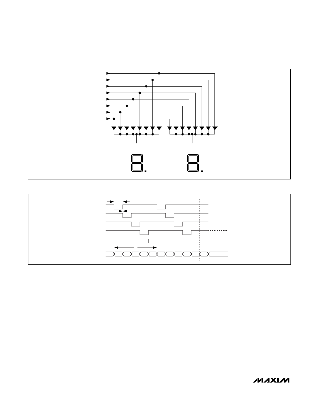
The MAX1365 has a 4.5-digit common-cathode display
driver, and the MAX1367 has a 3.5-digit common-cathode display driver. In addition, the LED drivers of the
MAX1365/MAX1367 feature peak-detection and datahold circuitry.
Figures 2 and 3 show the connection schemes for a
standard seven-segment LED display. The LED update
rate is 2.5Hz. Figure 4 shows a typical common-cathode configuration for two digits. In common-cathode
configuration, the cathodes of all LEDs in a digit are
connected together. Each segment driver of the
MAX1365/MAX1367 connects to its corresponding
LED’s anodes. For example, segment driver SEGA connects to all LED segments designated as A. Similar
configurations are used for other segment drivers.
Hz
Z
N
Hf
N
N
f
f
f
f
N
Z
m
m
()
()
()
sin
sin
()
=
−
=
−
−
−
11
1
1
4
4
1
π
π
sin( )x
x
4
FREQUENCY (Hz)
GAIN (dB)
5040302010
-160
-120
-80
-40
0
-200
060
Figure 1. Frequency Response of the SINC4Filter (Notch at 60Hz)
Page 13

The MAX1365/MAX1367 use a multiplexing scheme to
drive one digit at a time. The scan rate is fast enough to
make the digits appear to be lit. Figure 5 shows the
data-timing diagram for the MAX1365/MAX1367 where
T is the display scan period (typically around 1/512Hz
or 1.9531ms). TONin Figure 5 denotes the amount of
time each digit is on and is calculated as follows:
Decimal-Point Control
The MAX1365/MAX1367 allow for full decimal-point
control and feature leading-zero suppression.
Use the DPON, DPSET1, and DPSET2 bits in the control register to set the value of the decimal point (Tables
2 and 3). The MAX1365/MAX1367 overrange and
underrange display is shown in Table 4.
Leading-Zero Suppression
The MAX1365/MAX1367 include a leading-zero suppression circuitry to turn off unnecessary zeros. For
example, when DPSET1 and DPSET2 = [0,0], 0.0 is displayed instead of 000.0 (MAX1365). This feature saves
a substantial amount of power by not lighting unnecessary LEDs.
Interdigit Blanking
The MAX1365/MAX1367 also include an interdigitblanking circuitry. Without this feature, it is possible to
see a faint digit next to a digit that is completely on.
The interdigit-blanking circuitry prevents ghosting over
into the next digit for a short period of time. The typical
interdigit blanking time is 4µs.
T
Tms
s
ON
== =
5
1 95312
5
390 60.. µ
MAX1365/MAX1367
Stand-Alone, 4.5-/3.5-Digit Panel Meters
with 4–20mA Output
______________________________________________________________________________________ 13
A
B
C
A AAA
D
DIGIT 4 DIGIT 3 DIGIT 2 DIGIT 1 DIGIT 0
D DDD
E
G
F
EEE
GGGG
F FFF
BBBB
CC CC
DP DP DP DP DP
Figure 2. Segment Connection for the MAX1365 (4.5 Digits)
A
B
AA A
D
DIGIT 4 DIGIT 3 DIGIT 2 DIGIT 1
DDD
E
G
F
EE
GGG
FFF
BBB
CC C
DP DP DP DP
C
Figure 3. Segment Connection for the MAX1367 (3.5 Digits)
HOLD PEAK DISPLAY VALUES FORM
1XHold value
01Peak value
00Latest ADC result
Table 1. LED Priority Table
X = Don’t care.
DPON
DPSET1
DPSET2
DISPLAY
ZERO INPUT
READING
10 0 1888. 0.
10 1 188.8 0.0
11 0 18.88 0.00
11 1 1.888 0.000
Table 3. Decimal-Point Control Table—
MAX1367
CONDITION MAX1367 MAX1365
Overrange 1--- 1----
Underrange -1--- -1----
Table 4. LED During Overrange and
Underrange Conditions
DPON
DPSET1
DPSET2
DISPLAY
ZERO INPUT
READING
00 018888 0
00 118888 0
01 018888 0
01 118888 0
10 01888.8 0.0
10 1188.88 0.00
11 018.888 0.000
11 11.8888 0.0000
Table 2. Decimal-Point Control Table—
MAX1365
OUTPUT
OUTPUT
Page 14
Current Output
The MAX1365/MAX1367 feature a 4–20mA (0 to 16mA)
current output for driving remote panel meters, data loggers, and process controllers in industrial applications.
The DAC output is proportional to the input of the ADC
and LED display. In the simplest configuration, connect
DAC_VOUT directly to CONV_IN to have the current output (4–20mA or 0 to 16mA) follow the analog inputs.
Custom signal conditioning can be inserted between
DAC_VOUT and CONV_IN, or CONV_IN can be driven
independently by a voltage source if desired. See
Figures 11–14 for the transfer functions of the DAC and
V/I converter.
Note: The MAX1365/MAX1367 expect a 6kΩ (typ)
source impedance from the external voltage source
driving CONV_IN.
Current Offset
Set EN_I high for a current span of 4–20mA. Set EN_I low
for a current span of 0 to 16mA. See Table 5 for current
output.
Unipolar Mode
Set EN_BPM low to engage unipolar operation. In
unipolar mode, the current output at 4-20OUT (4–20mA
or 0 to 16mA) maps the analog input voltage (0 to 2V or
0 to 200mV). Negative voltages at the analog input
result in a 4mA or 0mA output, depending on the EN_I
setting. See Table 5 for current output. See Figures 12
and 13.
MAX1365/MAX1367
Stand-Alone, 4.5-/3.5-Digit Panel Meters
with 4–20mA Output
14 ______________________________________________________________________________________
A
A
A
DIGIT 1 DIGIT 2
SEGDP
SEGG
SEGF
SEGE
SEGD
SEGC
SEGB
SEGA
DD
EE
GG
FF
BB
CC
DP DP
B C D E F G DP A B C D E F G DP
Figure 4. 2-Digit Common-Cathode Configuration
143210432 04
T
T
ON
DIGIT 4 (MSD)
DIGIT 3
INTERDIGIT BLANKING TIME
DIGIT 2
DIGIT 1
DIGIT 0 (LSD)
DATA
MSD LSD
Figure 5. LED Voltage Waveform
Page 15

Bipolar Mode
Set EN_BPM high to engage bipolar operation. In bipolar mode, the current output at 4–20OUT (4–20mA or
0 to 16mA) maps the analog input voltage (±2V or
±200mV). In bipolar mode, a 0V analog input maps to
midscale (12mA). See Table 5 for current output (see
Figures 12 and 13).
5.2V Linear Regulator with Compensation
The MAX1365/MAX1367 feature a 5.2V linear regulator.
The 5.2V regulator consists of an op amp and connections to an external depletion-mode FET. The 5.2V regulator regulates the loop voltage that powers the
voltage-to-current converter and the rest of the transmitter circuitry. The regulator output voltage is available
at REG_VDD and is given by the equation:
V
REG_VDD
= 2.54 x V
REF+
The FET breakdown and saturation voltages determine
the usable range of loop voltages (V
EXT
). The external
FET parameters such as VGS(off), I
DSS
, and transconductance must be chosen so that the op amp output on
the REG_FORCE pin can control the FET operating
point while swinging in the range from VREG_AMP to
REG_VDD. See the Selecting Depletion-Mode FET section in the Applications Information section.
Connect a 0.1µF capacitor between CMP and
REG_FORCE to ensure stable operation of the regulator.
Applications Information
Power-On Reset
At power-on, the digital filter and modulator circuits
reset. The MAX1365 allows 6s for the reference to stabilize before performing enhanced offset calibration.
MAX1365/MAX1367
Stand-Alone, 4.5-/3.5-Digit Panel Meters
with 4–20mA Output
______________________________________________________________________________________ 15
CURRENT OUTPUT (mA)
ANALOG INPUT
UNIPOLAR MODE
(EN_I = LOW)
UNIPOLAR MODE
(EN_I = HIGH)
BIPOLAR MODE
(EN_I = LOW)
BIPOLAR MODE
(EN_I = HIGH)
Negative Full Scale 0 4 0 4
0V 0 4 8 12
Positive Full Scale 16 20 16 20
Table 5. Current Output Table
MAX1365
MAX1367
AV
DD
DV
DD
10µF
10µF
0.1µF
0.1µF
0.1µF
0.1µF
ANALOG SUPPLY
FERRITE
BEAD
R
REF
R
R
ACTIVE
GAUGE
DUMMY
GAUGE
REF+
REF-
NEGV
AIN+
AIN-
4-20OUT
4–20mA/0 TO 16mA
CURRENT-LOOP
OUTPUT
GND
0.1µF
0.1µF
Figure 6. Strain-Gauge Application with the MAX1365/MAX1367
Page 16

MAX1365/MAX1367
During these 6s, the MAX1365 displays 1.2V to 1.5V
when a stable reference is detected. If a valid reference is not found, the MAX1365 times out after 6s and
begins enhanced offset calibration. Enhanced offset
calibration typically lasts 2s. The MAX1365 begins converting after enhanced offset calibration.
Reference
ADC Reference
The MAX1365/MAX1367 reference sets the full-scale
range of the ADC transfer function. With a nominal
2.048V reference, the ADC full-scale range is ±2V with
RANGE = GND. With RANGE = DV
DD,
the full-scale
range is ±200mV. A decreased reference voltage
decreases full-scale range (see the Transfer Functions
section).
The ADC of the MAX1365/MAX1367 can accept either
an external reference or an internal reference (INTREF).
The INTREF logic selects the reference mode. For internal-reference operation, set INTREF to DV
DD,
connect
REF- to GND, and bypass REF+ to GND with a 4.7µF
capacitor. The internal reference provides a nominal
2.048V source between REF+ and GND. The internalreference temperature coefficient is typically
40ppm/°C.
For external-reference operation, set INTREF to GND.
REF+ and REF- are fully differential. For a valid external-reference input, VREF+ must be greater than VREF-.
Bypass REF+ and REF- with a 0.1µF or greater capacitor to GND in external-reference mode.
Figure 6 shows the MAX1365/MAX1367 operating with
an external differential reference. In this figure, REF- is
connected to the top of the strain gauge and REF+ is
connected to the midpoint of the resistor-divider of
the supply.
DAC Reference
The DAC of the MAX1365/MAX1367 accept either an
external reference or an internal reference. The REFSELE
enables or disables the internal reference. For externalreference operation, disable the DAC reference buffer by
setting REFSELE to DVDDand connect a voltage source
to REF_DAC.
For internal-reference operation, enable the DAC reference buffer by setting REFSELE to GND. In this mode,
leave REFDAC floating.
In either internal or external reference operation,
bypass REF_DAC with a 0.1µF capacitor to GND.
Choose a reference with output impedance (load regulation equivalent) of 100mΩ or less, such as the
MAX6126. For best performance, use an external
reference source for the ADC and DAC.
DAC Operation
For the MAX1365/MAX1367, a voltage proportional to
the ADC input is available at DACVOUT. Connect
DACVOUT to CONV_IN for normal operation. See
Figure 11 for the DAC transfer function.
Offset Calibration
The MAX1365/MAX1367 offer on-chip offset calibration.
The device offset calibrates during every conversion cycle.
Enhanced Offset Calibration
Enhanced offset calibration is a more accurate calibration method that is needed in the case of the ±200mV
range and 4.5-digit resolution. In addition to enhanced
offset calibration at power-up, the MAX1365/MAX1367
perform enhanced calibration on demand by connecting HOLD to AVDDfor > 2s.
Peak
The MAX1365/MAX1367 feature peak-detection circuitry.
When activated, the devices display only the highest
voltage measured to the LED. First, the current ADC
result is displayed. The new ADC conversion result is
compared to the current result. If the new value is larger than the previous peak value, the new value is displayed. If the new value is less than the previous peak
value, the display remains unchanged. Connect PEAK
to GND to clear the peak value and disable the peak
function. See Table 1 for LED Display priority.
Hold
The MAX1365/MAX1367 feature data-hold circuitry.
When activated, the device holds the current reading
on the LED.
Strain-Gauge Measurement
Connect the differential inputs of the MAX1365/
MAX1367 to the bridge network of the strain gauge. In
Figure 6, the analog supply voltage powers the bridge
network and the MAX1365/MAX1367, along with the
reference voltage. The MAX1365/MAX1367 handle an
analog input voltage range of ±200mV and ±2V full
scale. The analog/reference inputs of the parts allow
the analog input range to have an absolute value of
anywhere between -2.2V and +2.2V.
Stand-Alone, 4.5-/3.5-Digit Panel Meters
with 4–20mA Output
16 ______________________________________________________________________________________
Page 17

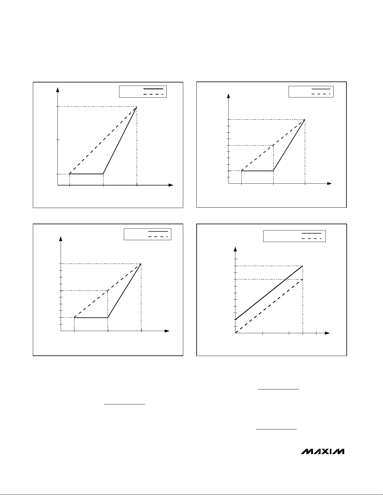
Transfer Functions
ADC Transfer Functions
Figures 7–10 show the transfer functions of the
MAX1365/MAX1367. The output data is stored in the
ADC data register in two’s complement.
The transfer function for the MAX1365 with AIN+ - AIN≥ 0 and RANGE = GND is:
The transfer function for the MAX1365 with AIN+ - AIN< 0 and RANGE = GND is:
The transfer function for the MAX1367 with AIN+ - AIN≥ 0 and RANGE = GND is:
() .31024 2000COUNT
VV
VV
x
AIN AIN
REF REF
=
+
−
−
+
−
−
() . ,21024 20 000 1COUNT
VV
VV
x
AIN AIN
REF REF
=
+
+
−
−
+
−
−
() . ,11024 20 000COUNT
VV
VV
x
AIN AIN
REF REF
=
+
−
−
+
−
−
MAX1365/MAX1367
Stand-Alone, 4.5-/3.5-Digit Panel Meters
with 4–20mA Output
______________________________________________________________________________________ 17
-2V
0
ANALOG INPUT VOLTAGE
+2V
LED
1 - - - -
19,999
2
1
0
- 0
- 1
- 2
-19,999
- 1 - - - -
-100µV
100µV
Figure 7. MAX1365 Transfer Function—±2V Range
-200mV
0
ANALOG INPUT VOLTAGE
+200mV
LED
1 - - - -
19,999
2
1
0
- 0
- 1
- 2
-19,999
- 1 - - - -
-10µV
10µV
Figure 8. MAX1365 Transfer Function—±200mV Range
-2V
0
ANALOG INPUT VOLTAGE
+2V
LED
1 - - -
1999
2
1
0
- 0
- 1
- 2
-1999
- 1 - - -
-1mV
1mV
Figure 10. MAX1367 Transfer Function—±2V Range
-200mV
0
ANALOG INPUT VOLTAGE
+200mV
LED
1 - - -
1999
2
1
0
- 0
- 1
- 2
-1999
- 1 - - -
-100µV
100µV
Figure 9. MAX1367 Transfer Function—±200mV Range
Page 18
MAX1365/MAX1367
The transfer function for the MAX1367 with AIN+ - AIN< 0 and RANGE = GND is:
The transfer function for the MAX1365 with AIN+ - AIN≥ 0 and RANGE = DV
DD
is:
The transfer function for the MAX1365 with AIN+ - AIN< 0 and RANGE = DV
DD
is:
() . ,61024 20 000 10 1COUNT
VV
VV
xx
AIN AIN
REF REF
=
+
+
−
−
+
−
−
() . ,51024 20 000 10COUNT
VV
VV
xx
AIN AIN
REF REF
=
+
−
−
+
−
−
() .41024 2000 1COUNT
VV
VV
x
AIN AIN
REF REF
=
+
+
−
−
+
−
−
Stand-Alone, 4.5-/3.5-Digit Panel Meters
with 4–20mA Output
18 ______________________________________________________________________________________
- FS + FS
ADC OUTPUT CODE
0
DAC OUTPUT VOLTAGE (V)
0
1. 25
UNIPOLAR :
BIPLOLAR :
FS = FULL SCALE
Figure 11. DAC Output Voltage vs. ADC Output Code
UNIPOLAR :
BIPLOLAR :
ADC OUTPUT CODE
4-20OUT (mA)
20
FS = FULL SCALE
0
16
4
- FS + FS
0
CURRENT
OFFSET
ENABLED
(EN_I = 1)
12
Figure 12. Output Current (4-20OUT) vs. ADC Output Code
(Current Offset Enabled)
OFFSET ENABLED :
OFFSET DISABLED :
V/I CONVERTER INPUT ( V )
0
4-20OUT (mA)
20
0
16
4
1. 25
Figure 14. 4-20OUT Output Current vs. V/I Converter Input
Voltage
UNIPOLAR :
BIPLOLAR :
ADC OUTPUT CODE
4-20OUT (mA)
16
FS = FULL SCALE
0
- FS + FS
0
CURRENT
OFFSET
DISABLED
(EN_I = 0)
8
Figure 13. Output Current (4-20OUT) vs. ADC Output Code
(Current Offset Disabled)
Page 19

The transfer function for the MAX1367 with AIN+ - AIN≥ 0 and RANGE = DV
DD
is:
The transfer function for the MAX1367 with AIN+ - AIN< 0 and RANGE = DV
DD
is:
DAC Transfer Functions
Figure 11 shows the DAC transfer function for the
MAX1365/MAX1367 in unipolar and bipolar modes.
The transfer function for the DAC in the MAX1365/
MAX1367 unipolar mode is:
where N = two’s complement ADC output code.
In unipolar mode, V
DACVOUT
is equal to 0V for all two’s
complement ADC codes less than zero (see Figure 12).
The transfer function for the DAC in the MAX1365/
MAX1367 in bipolar mode is:
where N = two’s complement ADC output.
Voltage-to-Current Transfer Function
Figures 12 and 13 show the MAX1365/MAX1367 transfer function of the output current (4-20OUT) versus the
ADC input code.
The transfer function for the MAX1365/MAX1367 with
the current offset enabled (EN_I is high) is:
The transfer function for the MAX1365/MAX1367 with
the current offset disabled (EN_I is low) is:
Supplies, Layout, and Bypassing
Power up AVDDand DVDDbefore applying an analog
input and external-reference voltage to the device. If
this is not possible, limit the current into these inputs to
50mA. When the analog and digital supplies come from
the same source, isolate the digital supply from the
analog supply with a low-value resistor (10Ω) or ferrite
bead. For best performance, ground the MAX1365/
MAX1367 to the analog ground plane of the circuit
board. Avoid running digital lines under the device as
this can couple noise onto the IC. Run the analog
ground plane under the MAX1365/MAX1367 to minimize coupling of digital noise. Make the power-supply
lines to the MAX1365/MAX1367 as wide as possible to
provide low-impedance paths and reduce the effects of
glitches on the power-supply line. Shield fast-switching
signals, such as clocks, with digital ground to avoid
radiating noise to other sections of the board. Avoid
running clock signals near the analog inputs. Avoid
crossover of digital and analog signals. Running traces
that are on opposite sides of the board at right angles to
each other reduces feedthrough effects. Good decoupling is important when using high-resolution ADCs.
Decouple the supplies with 0.1µF ceramic capacitors to
GND. Place these components as close to the device
as possible to achieve the best decoupling.
Selecting Segment Current
A resistor from ISET to ground sets the current for each
LED segment. See Table 6 for more detail. Use the following formula to set the segment current:
R
ISET
values below 25kΩ increase the I
SEG
. However,
the internal current-limit circuit limits the I
SEG
to less than
30mA. At higher I
SEG
values, proper operation of the
device is not guaranteed. In addition, the power dissipated may exceed the package power-dissipation limit.
Choosing Supply Voltage to Minimize
Power Dissipation
The MAX1365/MAX1367 drive a peak current of 25.5mA
into LEDs with a 2.2V forward voltage drop when operated from a supply voltage of at least 3.0V. Therefore, the
minimum voltage drop across the internal LED drivers is
0.8V (3.0V - 2.2V = 0.8V). The MAX1365/MAX1367 sink
when the outputs are operating and the LED segment
drivers are at full current (8 x 25.5mA = 204mA). For a
3.3V supply, the MAX1365/MAX1367 dissipate 224.4mW
((3.3V - 2.2V) x 204 = 224.4mW). If a higher supply voltage is used, the driver absorbs a higher voltage, and the
driver’s power dissipation increases accordingly.
I
V
R
x
SEG
ISET
=
120
450
.
IOUT
mA
xV
CONV IN
≅
16
125.
_
IOUT
mA
xV mA
CONV IN
≅+
16
1254.
_
V
N
xV
DACVOUT REF
=
+19 999
65 536,,
V
N
xV
DACVOUT REF
=
−32 768 1,
() .81024 2000 10 1COUNT
VV
VV
xx
AIN AIN
REF REF
=
+
+
−
−
+
−
−
() .71024 2000 10COUNT
VV
VV
xx
AIN AIN
REF REF
=
+
−
−
+
−
−
MAX1365/MAX1367
Stand-Alone, 4.5-/3.5-Digit Panel Meters
with 4–20mA Output
______________________________________________________________________________________ 19
Note: The input at V
CONV_IN
expects a source imped-
ance of typically 6kΩ when driving V
CONV_IN
externally.
Page 20

MAX1365/MAX1367
However, if the LEDs used have a higher forward voltage
drop than 2.2V, the supply voltage must be raised
accordingly to ensure that the driver always has at least
0.8V headroom. For a LEDV supply voltage of 2.7V, the
maximum LED forward voltage is 1.9V to ensure 0.8V driver headroom. The voltage drop across the drivers with
a nominal +5V supply (5.0V - 2.2V = 2.8V) is almost
three times the drop across the drivers with a nominal
3.3V supply (3.3V - 2.2V = 1.1V). Therefore, the driver’s
power dissipation increases three times. The power dissipation in the part causes the junction temperature to
rise accordingly. In the high ambient temperature case,
the total junction temperature may be very high
(> +125°C). At higher junction temperatures, the ADC
performance degrades. To ensure the dissipation limit
for the MAX1365/MAX1367 is not exceeded and the
ADC performance is not degraded; a diode can be
inserted between the power supply and LEDV.
Selecting Depletion-Mode FET
An external depletion-mode FET (DMOS) works in conjunction with the regulator circuit to supply the V/I converter with loop power. REG_FORCE regulates the gate
of the DMOS so that the drain voltage is 5.2V (typ) and
allows the 4–20mA (0 to 16mA) loop to be directly powered from a 7V to 30V supply. DMOS I
DS
consists of the
current output at 4-20OUT, a 4mA offset current, and
1mA (typ) consumed by the V/I converter.
For offset-enabled mode (EN_I = 1):
IDS= I
4-20OUT
+ 4mA + 1mA
where I
DS
is the current in the DMOS.
For offset-disabled mode (EN_I = 0):
IDS= I
4-20OUT
+ 1mA
where I
DS
is the current in the DMOS.
Table 7 provides the FET characteristics for selecting
an external DMOS transistor. The DN25D FET transistor
from Supertex meets all the requirements of Table 7.
Other suitable transistors include ND2020L and
ND2410L from Siliconix.
Connect a 0.1µF capacitor between CMP and
REG_FORCE to ensure stable regulator compensation.
Definitions
Integral Nonlinearity (INL)
INL is the deviation of the values on an actual transfer
function from a straight line. This straight line is either a
best-straight-line fit or a line drawn between the end
points of the transfer function, once offset and gain
errors have been nullified. INL for the MAX1365/
MAX1367 is measured using the end-point method.
Differential Nonlinearity (DNL)
DNL is the difference between an actual step width and
the ideal value of ±1 LSB. A DNL error specification of
less than ±1 LSB guarantees no missing codes and a
monotonic transfer function.
Rollover Error
Rollover error is defined as the absolute-value difference between a near positive full-scale reading and
near negative full-scale reading. Rollover error is tested
by applying a full-scale positive voltage, swapping
AIN+ and AIN-, and adding the results.
Zero-Input Reading
Ideally, with AIN+ connected to AIN-, the MAX1365/
MAX1367 LED displays zero. Zero-input reading is the
measured deviation from the ideal zero and the actual
measured point.
Gain Error
Gain error is the amount of deviation between the measured full-scale transition point and the ideal full-scale
transition point.
Common-Mode Rejection (CMR)
CMR is the ability of a device to reject a signal that is
common to both input terminals. The common-mode
signal can be either an AC or a DC signal or a combination of the two. CMR is often expressed in decibels.
Normal-Mode 50Hz and 60Hz Rejection
(Simultaneously)
Normal-mode rejection is a measure of how much output
changes when 50Hz and 60Hz signals are injected into
only one of the differential inputs. The MAX1365/
MAX1367 sigma-delta converter uses its internal digital
filter to provide normal-mode rejection to both 50Hz and
60Hz power-line frequencies simultaneously.
Stand-Alone, 4.5-/3.5-Digit Panel Meters
with 4–20mA Output
20 ______________________________________________________________________________________
Page 21
Power-Supply Rejection (PSR)—ADC
PSR is a measure of the data converter’s level of immunity to power-supply fluctuations. PSR assumes that the
converter’s linearity is unaffected by changes in the
power-supply voltage. Power-supply rejection ratio
(PSRR) is the ratio of the input signal change to the
change in the converter output. PSRR is typically measured in dB.
Power-Supply Rejection—V/I Converter
PSR is a measure of the data converter’s level of immunity to power-supply fluctuations. PSR assumes that the
converter’s linearity is unaffected by changes in the
power-supply voltage.
Note: The V/I converter current output (4–20mA)
power-supply rejection is with respect to the 7V to 30V
loop supply.
MAX1365/MAX1367
Stand-Alone, 4.5-/3.5-Digit Panel Meters
with 4–20mA Output
______________________________________________________________________________________ 21
R
SET
(kΩ)I
SEG
(mA)
25 21.6
50 10.8
100 5.4
500 1.1
> 2500 LED driver disabled
Table 6. Segment-Current Selection
FET TYPE
N-CHANNEL DEPLETION MODE
I
DS
30mA
BV
DS
(V
EXT
* - REG_VDD) min
V
PINCHOFF
REG_VDD max
Power dissipation 30mA x (V
EXT
- REG_VDD) min
Table 7. FET Characteristics
*V
EXT
is the 7V to 30V loop voltage.
Page 22

MAX1365/MAX1367
Stand-Alone, 4.5-/3.5-Digit Panel Meters
with 4–20mA Output
22 ______________________________________________________________________________________
MAX1365
MAX6126
0.1µF 10µF
10µF
0.1µF
0.1µF
10µF
10µF
L
ISO
R
L
2.7V TO
5.25V
4.75V TO
5.25V
DEPLETION-
MODE
FET
V
EXT
7V TO 30V
4-20mA
PLC INPUT
ADC
AIN+
IN
DAC_VDD
SUPPLY VOLTAGE
0.1µF
AIN-
LEDV
4-20mA/0 TO 16mA
CURRENT-LOOP OUTPUT
LED_EN
DV
DD
AV
DD
DAC_VDD
GND_DAC REF_DAC
SET
NEGV GND REF- REF+ GND_V/ILEDG
DACVOUT
OUTF
OUTS
CONV_IN
EN_BPM
EN_I
TO DV
DD
DACDATA_SEL
CS_DAC
REFSELE
INTREF
RANGE
PEAK
HOLD
DPON
DPSET2
DPSET1
DIG0–DIG4
DIGIT
CONNECTIONS
SEGA–SEGDP
SEGMENT
CONNECTIONS
V
IN
CMP
GNDS GND
REG_FORCE
REG_VDD
REG_AMP
4-20OUT
25kΩ
0.1µF
0.1µF
MAX1365 Typical Operating Circuit
Page 23

MAX1365/MAX1367
Stand-Alone, 4.5-/3.5-Digit Panel Meters
with 4–20mA Output
______________________________________________________________________________________ 23
MAX1367
MAX6126
0.1µF 10µF
10µF
0.1µF
0.1µF
10µF
10µF
L
ISO
R
L
2.7V TO
5.25V
4.75V TO
5.25V
DEPLETION-
MODE
FET
V
EXT
7V TO 30V
4-20mA
PLC INPUT
ADC
AIN+
IN
DAC_VDD
SUPPLY VOLTAGE
0.1µF
AIN-
LEDV
4-20mA/0 TO 16mA
CURRENT-LOOP OUTPUT
LED_EN
DV
DD
AV
DD
DAC_VDD
GND_DACDIGO REF_DAC
SET
NEGV GND REF- REF+ GND_V/ILEDG
DACVOUT
OUTF
OUTS
CONV_IN
EN_BPM
EN_I
TO DV
DD
DACDATA_SEL
CS_DAC
REFSELE
INTREF
RANGE
PEAK
HOLD
DPON
DPSET2
DPSET1
DIG1–DIG4
DIGIT
CONNECTIONS
SEGA–SEGDP
SEGMENT
CONNECTIONS
V
IN
CMP
GNDS GND
REG_FORCE
REG_VDD
REG_AMP
4-20OUT
25kΩ
0.1µF
0.1µF
MAX1367 Typical Operating Circuit
Page 24

MAX1365/MAX1367
Stand-Alone, 4.5-/3.5-Digit Panel Meters
with 4–20mA Output
24 ______________________________________________________________________________________
TOP VIEW
MAX1365
MAX1367
TQFP
13
14
15
16
17
18
19
20
21
22
23
24
CONV_IN
4-200UT
GDN_DAC
GND_V/I
REF_DAC
EN_BPM
EN_I
REFSELE
DACDATA_SEL
CS_DAC
INTREF
RANGE
48
47
46
45
44
43
42
41
40
39
38
37
1
2
3 45678910
11
12
REF+
REF-
DPON
NEGV
LED_EN
SEGDP
SEGG
SEGF
SEGE
SEGD
SEGC
LEDV
DACVOUT
DAC_VDD
CMP
REG_AMP
REG_FORCE
REG_VDD
SET
DV
DDAVDD
GND
AIN-
AIN+
36
35
34 33 32 31 30 29 28 27
26
25
PEAK
HOLD
DPSET2
DPSET1
LEDG
DIG0
DIG1
DIG2
DIG3
DIG4
SEGA
SEGB
Pin Configuration
Chip Information
TRANSISTOR COUNT: 83,463
PROCESS: CMOS
Page 25

MAX1365/MAX1367
Stand-Alone, 4.5-/3.5-Digit Panel Meters
with 4–20mA Output
Maxim cannot assume responsibility for use of any circuitry other than circuitry entirely embodied in a Maxim product. No circuit patent licenses are
implied. Maxim reserves the right to change the circuitry and specifications without notice at any time.
Maxim Integrated Products, 120 San Gabriel Drive, Sunnyvale, CA 94086 408-737-7600 ____________________ 25
© 2006 Maxim Integrated Products Printed USA is a registered trademark of Maxim Integrated Products, Inc.
Package Information
(The package drawing(s) in this data sheet may not reflect the most current specifications. For the latest package outline information,
go to www.maxim-ic.com/packages
.)
32L/48L,TQFP.EPS
E
1
2
21-0054
PACKAGE OUTLINE, 32/48L TQFP, 7x7x1.4mm
E
2
2
21-0054
PACKAGE OUTLINE, 32/48L TQFP, 7x7x1.4mm
 Loading...