

Page 1

General Description
The MAX1363/MAX1364 low-power, 12-bit, 4-channel
analog-to-digital converters (ADCs) feature a digitally
programmable window comparator with an interrupt output for automatic system-monitoring applications. Once
configured, monitor mode automatically asserts an interrupt when any analog input exceeds the programmed
upper or lower thresholds, without interaction to the
host. The MAX1363/MAX1364 respond to the SMBus™
alert, allowing quick identification of the alarming device
on a shared interrupt. A programmable delay between
monitoring intervals lowers power consumption for
reduced monitoring rates.
In addition, the MAX1363/MAX1364 integrate an internal voltage reference, a clock, and a 1.7MHz, highspeed, I2C™-compatible, 2-wire serial interface. The
optimized interface allows a maximum conversion rate
of 94.4ksps in normal mode while reading back the
conversion results. Each of the four analog inputs is
configurable for single-ended or fully differential operation and unipolar or bipolar operation. Two scan modes
utilize on-chip random access memory (RAM) to allow
eight conversions of a selected channel or scanning of
a group of channels to reduce interface overhead.
These devices operate from a single 2.7V to 3.6V
(MAX1363) or 4.5V to 5.5V (MAX1364) supply and
require only 436µA at the maximum sampling rate of
133ksps in monitor mode and 670µA at the maximum
sampling rate of 94.4ksps. AutoShutdown™ powers
down the devices between conversions, reducing supply current to less than 1µA when idle.
The full-scale analog-input range is determined by the
internal reference or by an externally applied reference
voltage ranging from 1V to VDD. The MAX1363 features
a 2.048V internal reference, and the MAX1364 features
a 4.096V internal reference.
The MAX1363/MAX1364 are available in a 10-pin
µMAX®package and are specified over the extended
(-40°C to +85°C) temperature range. For 10-bit applications, refer to the pin-compatible MAX1361/MAX1362
data sheet.
Applications
System Monitoring/Supervision
Servers/Workstations
High-Reliability Power Supplies
Medical Instrumentation
Features
♦ Monitor Mode
Programmable Lower/Upper Trip Threshold
Alarm-Status Register Records Fault Events
SMBus Alert Response
Programmable Sampling Intervals
♦ 12-Bit, I2C-Compatible ADC
±1 LSB INL, ±1 LSB DNL
♦ 4-Channel Single-Ended or 2-Channel Fully
Differential Inputs
♦ Software-Programmable Bipolar/Unipolar
Conversions
♦ Fast Sampling Rate
94.4ksps While Continuously Reading
Conversions
133ksps in Monitor Mode
♦ High-Speed, I
2
C-Compatible Serial Interface
100kHz/400kHz Standard/Fast Mode
Up to 1.7MHz High-Speed Mode
Six Available I2C Slave Addresses
♦ Single Supply
2.7V to 3.6V (MAX1363)
4.5V to 5.5V (MAX1364)
♦ Internal Reference
2.048V (MAX1363)
4.096V (MAX1364)
♦ External Reference: 1V to V
DD
♦ Low Power
436µA in Monitor Mode (133ksps)
670µA at 94.4ksps
6µA at 1ksps
0.5µA in Power-Down Mode
♦ Small Package
10-Pin µMAX
MAX1363/MAX1364
4-Channel, 12-Bit System Monitors with Programmable
Trip Window and SMBus Alert Response
________________________________________________________________ Maxim Integrated Products 1
Ordering Information/Selector Guide
19-3338; Rev 0; 7/04
For pricing, delivery, and ordering information, please contact Maxim/Dallas Direct! at
1-888-629-4642, or visit Maxim’s website at www.maxim-ic.com.
SMBus is a trademark of Intel Corporation.
I
2
C is a trademark of Philips Corporation. Purchase of I2C components from Maxim Integrated Products, Inc. or one of its sublicensed Associated Companies, conveys a license under the
Philips I2C Patent Rights to use these components in an I2C system, provided that the system conforms to the I2C Standard
Specification as defined by Philips.
AutoShutdown is a trademark of Maxim Integrated Products, Inc.
µMAX is a registered trademark of Maxim Integrated Products, Inc.
Typical Operating Circuit and Pin Configuration appear at
end of data sheet.
Ordering Information/Selector Guide continued at end of data sheet.
*Future product—contact factory for availability.
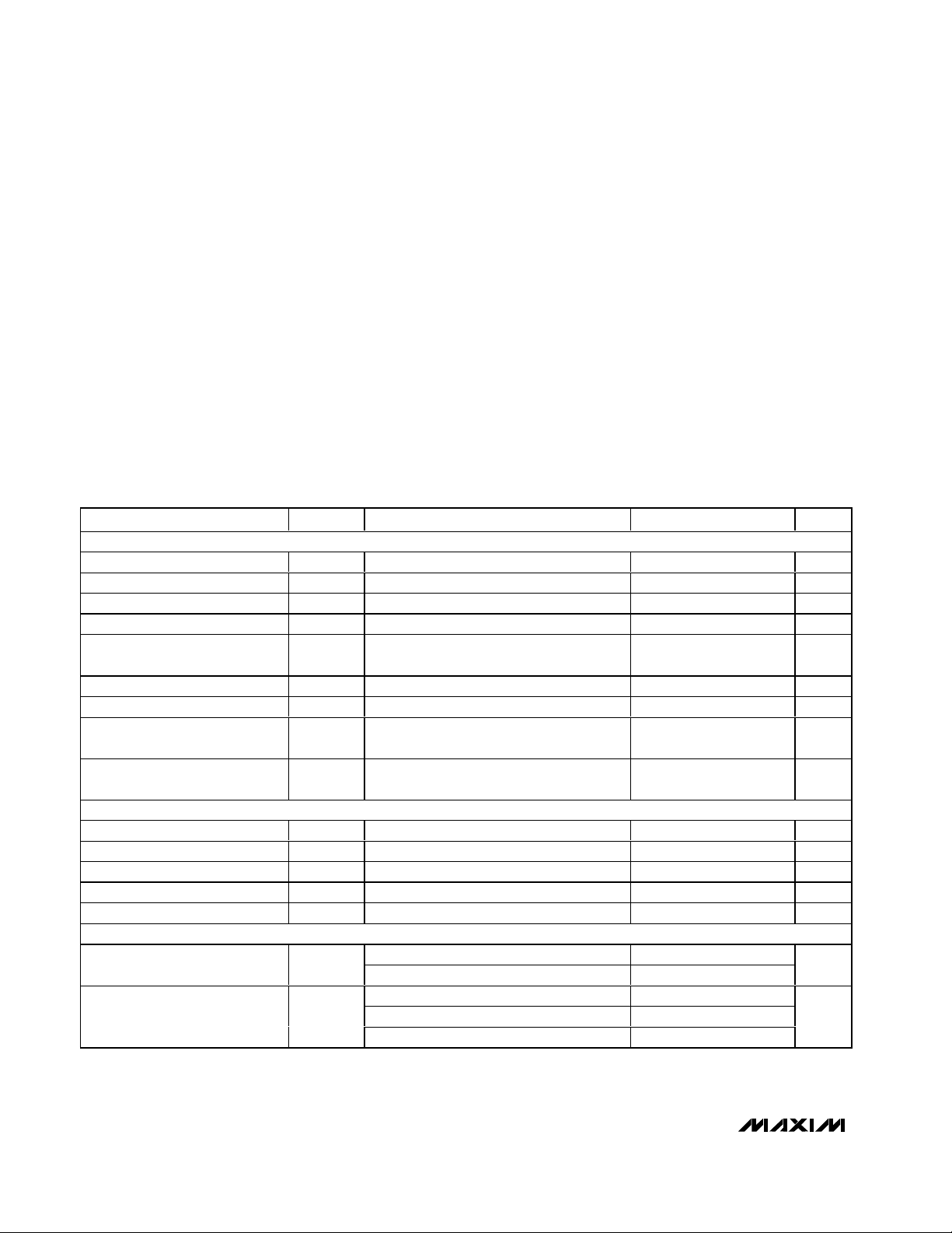
PART TEMP RANGE PIN-PACKAGE I2C SLAVE ADDRESS SUPPLY VOLTAGE (V)
MAX1363EUB -40°C to +85°C 10 µMAX 0110100/0110101 2.7 to 3.6
MAX1363LEUB* -40°C to +85°C 10 µMAX 0110010/0110011 2.7 to 3.6
MAX1363MEUB* -40°C to +85°C 10 µMAX 0110110/0110111 2.7 to 3.6
Page 2
MAX1363/MAX1364
4-Channel, 12-Bit System Monitors with Programmable
Trip Window and SMBus Alert Response
2 _______________________________________________________________________________________
ABSOLUTE MAXIMUM RATINGS
ELECTRICAL CHARACTERISTICS
(VDD= 2.7V to 3.6V (MAX1363), VDD= 4.5V to 5.5V (MAX1364), V
REF
= 2.048V (MAX1363), V
REF
= 4.096V (MAX1364), C
REF
=
0.1µF, f
SCL
= 1.7MHz, TA= T
MIN
to T
MAX
, unless otherwise noted. Typical values are at TA= +25°C.)
Stresses beyond those listed under “Absolute Maximum Ratings” may cause permanent damage to the device. These are stress ratings only, and functional
operation of the device at these or any other conditions beyond those indicated in the operational sections of the specifications is not implied. Exposure to
absolute maximum rating conditions for extended periods may affect device reliability.
VDDto GND..............................................................-0.3V to +6V
AIN0–AIN3, A0, REF to GND......................-0.3V to (V
DD
+ 0.3V)
SDA, SCL, INT to GND.............................................-0.3V to +6V
Maximum Current Into Any Pin.........................................±50mA
Continuous Power Dissipation (T
A
= +70°C)
10-Pin µMAX (derate 5.6mW/°C above +70°C) ........444.4mW
Operating Temperature Range ...........................-40°C to +85°C
Junction Temperature......................................................+150°C
Storage Temperature Range .............................-60°C to +150°C
Lead Temperature (soldering, 10s) .................................+300°C
DC ACCURACY (f
Resolution 12 Bits
Relative Accuracy INL (Note 2) ±1 LSB
Differential Nonlinearity DNL No missing codes ±1 LSB
Offset Error ±4 LSB
Offset-Error Temperature
Coefficient
Gain Error (Note 3) ±4 LSB
Gain Temperature Coefficient Relative to FSR 0.3 ppm/°C
Channel-to-Channel Offset
Matching
Channel-to-Channel Gain
Matching
DYNAMIC PERFORMANCE (f
Signal-to-Noise Plus Distortion SINAD 70 dB
Total Harmonic Distortion THD Up to the 5th harmonic -78 dB
Spurious-Free Dynamic Range SFDR 78 dB
Full-Power Bandwidth SINAD > 57dB 3.0 MHz
Full-Linear Bandwidth -3dB point 5.0 MHz
CONVERSION RATE
Conversion Time (Note 4) t
Throughput Rate (Note 5) f
PARAMETER SYMBOL CONDITIONS MIN TYP MAX UNITS
SAMPLE
= 94.4ksps) (Note 1)
IN(SINE-WAVE)
= 10kHz, V
CONV
SAMPLE
Relative to FSR 0.3 ppm/°C
IN(P-P)
Internal clock 7.5
External clock 10.6
Internal clock, SCAN[1:0] = 01 51
External clock 94.4
Monitor mode, SCAN[1:0] = 10 133
= V
REF
, f
SAMPLE
= 94.4ksps)
±0.1 LSB
±0.1 LSB
µs
ksps
Page 3
MAX1363/MAX1364
4-Channel, 12-Bit System Monitors with Programmable
Trip Window and SMBus Alert Response
_______________________________________________________________________________________ 3
ELECTRICAL CHARACTERISTICS (continued)
(VDD= 2.7V to 3.6V (MAX1363), VDD= 4.5V to 5.5V (MAX1364), V
REF
= 2.048V (MAX1363), V
REF
= 4.096V (MAX1364), C
REF
=
0.1µF, f
SCL
= 1.7MHz, TA= T
MIN
to T
MAX
, unless otherwise noted. Typical values are at TA= +25°C.)
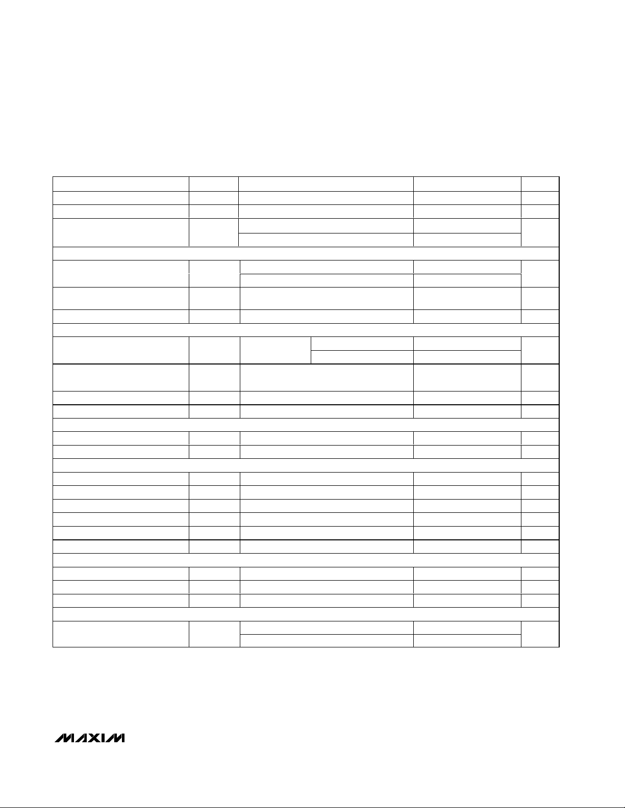
PARAMETER SYMBOL CONDITIONS MIN TYP MAX UNITS
Track/Hold Acquisition Time 800 ns
Internal Clock Frequency 2.8 MHz
Aperture Delay (Note 6) t
AD
External clock, fast mode 60
External clock, high-speed mode 30
ANALOG INPUT (AIN0–AIN3)
Input Voltage Range, Single
Ended and Differential (Note 7)
Input Multiplexer Leakage
Current
Input Capacitance C
Unipolar 0 V
Bipolar -V
ON/OFF-leakage current, V
IN
INTERNAL REFERENCE (Note 8)
Reference Voltage V
Reference-Voltage Temperature
Coefficient
TCV
REF
TA = +25°C
REF
REF Short-Circuit Current 2mA
REF Source Impedance 1.5 kΩ
EXTERNAL REFERENCE
REF Input Voltage Range V
REF Input Current I
REF
REF
(Note 9) 1 V
f
= 94.4ksps 40 µA
SAMPLE
DIGITAL INPUTS/OUTPUTS (SCL, SDA, A0)
Input High Voltage V
Input Low Voltage V
Input Hysteresis V
Input Current I
Input Capacitance C
Output Low Voltage V
IH
IL
HYST
IN
IN
OL
I
= 3mA 0.4 V
SINK
INT OUTPUT
Output Low Voltage I
= 3mA 0.4 V
SINK
INT Leakage Current No faults detected ±10 µA
Output Capacitance 15 pF
POWER REQUIREMENTS
Supply Voltage V
DD
MAX1363 2.7 3.6
MAX1364 4.5 5.5
= 0 or V
AIN_
DD
/ 2 +V
REF
REF
±0.01 ±1 µA
REF
22 pF
MAX1363 2.027 2.048 2.068
MAX1364 4.055 4.096 4.137
25 ppm/°C
DD
0.7 x V
DD
0.3 x V
0.1 x V
DD
±10 µA
15 pF
/ 2
DD
ns
V
V
V
V
V
V
V
Page 4
MAX1363/MAX1364
4-Channel, 12-Bit System Monitors with Programmable
Trip Window and SMBus Alert Response
4 _______________________________________________________________________________________
ELECTRICAL CHARACTERISTICS (continued)
(VDD= 2.7V to 3.6V (MAX1363), VDD= 4.5V to 5.5V (MAX1364), V
REF
= 2.048V (MAX1363), V
REF
= 4.096V (MAX1364), C
REF
=
0.1µF, f
SCL
= 1.7MHz, TA= T
MIN
to T
MAX
, unless otherwise noted. Typical values are at TA= +25°C.)
Supply Current I
Shutdown Current
Power-Supply Rejection Ratio PSRR Full-scale input (Note 11) ±0.01 ±0.5 LSB/V
TIMING CHARACTERISTICS FOR FAST MODE (Figures 1a, 2)
Serial Clock Frequency f
Bus Free Time Between a
STOP (P) and a
START (S) Condition
PARAMETER SYMBOL CONDITIONS MIN TYP MAX UNITS
f
SAMPLE
133ksps,
monitor mode
(Note 10)
f
SAMPLE
94.4ksps,
external clock
f
SAMPLE
40ksps,
internal clock
f
SAMPLE
10ksps,
internal clock
f
SAMPLE
1ksps,
internal clock
f
SAMPLE
133ksps,
monitor mode
(Note10)
f
SAMPLE
94.4ksps,
external clock
f
SAMPLE
40ksps,
internal clock
f
SAMPLE
10ksps,
internal clock
f
SAMPLE
1ksps, internal
clock
SCL
t
BUF
MAX1363
DD
MAX1364
Internal reference on 333
Internal reference off 0.5 10
=
Internal reference 660 1600
External reference 436 1350
=
Internal reference 900 1150
External reference 670 900
=
Internal reference 530
External reference 230
=
Internal reference 380
External reference 60
=
Internal reference 330
External reference 6
=
Internal reference 660 1600
External reference 436 1350
=
Internal reference 900 1150
External reference 670 900
=
Internal reference 530
External reference 230
=
Internal reference 380
External reference 60
=
Internal reference 330
External reference 6
1.3 µs
400 kHz
µA
µA
Page 5
MAX1363/MAX1364
4-Channel, 12-Bit System Monitors with Programmable
Trip Window and SMBus Alert Response
_______________________________________________________________________________________ 5
ELECTRICAL CHARACTERISTICS (continued)
(VDD= 2.7V to 3.6V (MAX1363), VDD= 4.5V to 5.5V (MAX1364), V
REF
= 2.048V (MAX1363), V
REF
= 4.096V (MAX1364), C
REF
=
0.1µF, f
SCL
= 1.7MHz, TA= T
MIN
to T
MAX
, unless otherwise noted. Typical values are at TA= +25°C.)
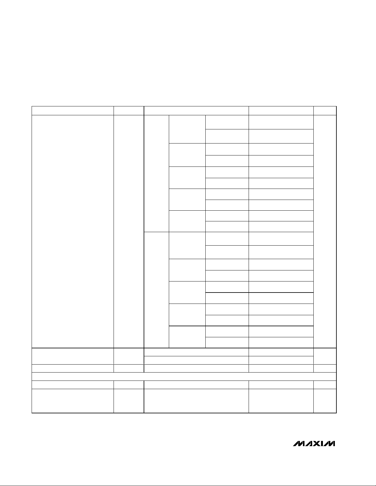
PARAMETER SYMBOL CONDITIONS MIN TYP MAX UNITS
Hold Time for START (S)
Condition
Low Period of the SCL Clock t
High Period of the SCL Clock t
Setup Time for a Repeated
START Condition (Sr)
Data Hold Time t
Data Setup Time t
Rise Time of Both SDA and SCL
Signals, Receiving
Fall Time of SDA Transmitting
Setup Time for STOP (P)
Condition
Capacitive Load for Each Bus
Line
t
HD, STA
LOW
HIGH
t
SU, STA
HD, DAT
SU, DAT
t
t
t
SU, STO
C
Measured from 0.3VDD to 0.7V
R
Measured from 0.3VDD to 0.7V
F
B
Pulse Width of Spike Suppressed 50 ns
TIMING CHARACTERISTICS FOR HIGH-SPEED MODE (CB = 400pF, Figures 1a, 2) (Note 12)
Serial Clock Frequency f
Hold Time, Repeated START
Condition (Sr)
t
Low Period of the SCL Clock t
High Period of the SCL Clock t
Setup Time for a Repeated
START Condition (Sr)
t
Data Hold Time t
Data Setup Time t
Rise Time of SCL Signal, Current
Source Enabled
Rise Time of SCL Signal After
Acknowledge Bit
Fall Time of SCL Signal t
Rise Time of SDA Signal t
Fall Time of SDA Signal t
Setup Time for STOP (P)
Condition
t
Capacitive Load for Each Bus
Line
SCLH
HD, STA
LOW
HIGH
SU, STA
HD, DAT
SU, DAT
t
RCL
t
RCL1
FCL
RDA
FDA
SU, STO
C
(Note 13) 1.7 MHz
(Note 13) 320 ns
(Note 14) 0 150 ns
Measured from 0.3VDD to 0.7V
Measured from 0.3VDD to 0.7V
Measured from 0.3VDD to 0.7V
Measured from 0.3VDD to 0.7V
Measured from 0.3VDD to 0.7V
(Notes 13, 14) 400 pF
B
Pulse Width of Spike Suppressed 0 10 ns
DD
DD 0
DD
DD
DD
DD
DD
0.6 µs
1.3 µs
0.6 µs
0.6 µs
0 900 ns
100 ns
0 300 ns
300 ns
0.6 µs
400 pF
160 ns
120 ns
160 ns
10 ns
20 80 ns
20 160 ns
20 80 ns
20 160 ns
20 160 ns
160 ns
Page 6
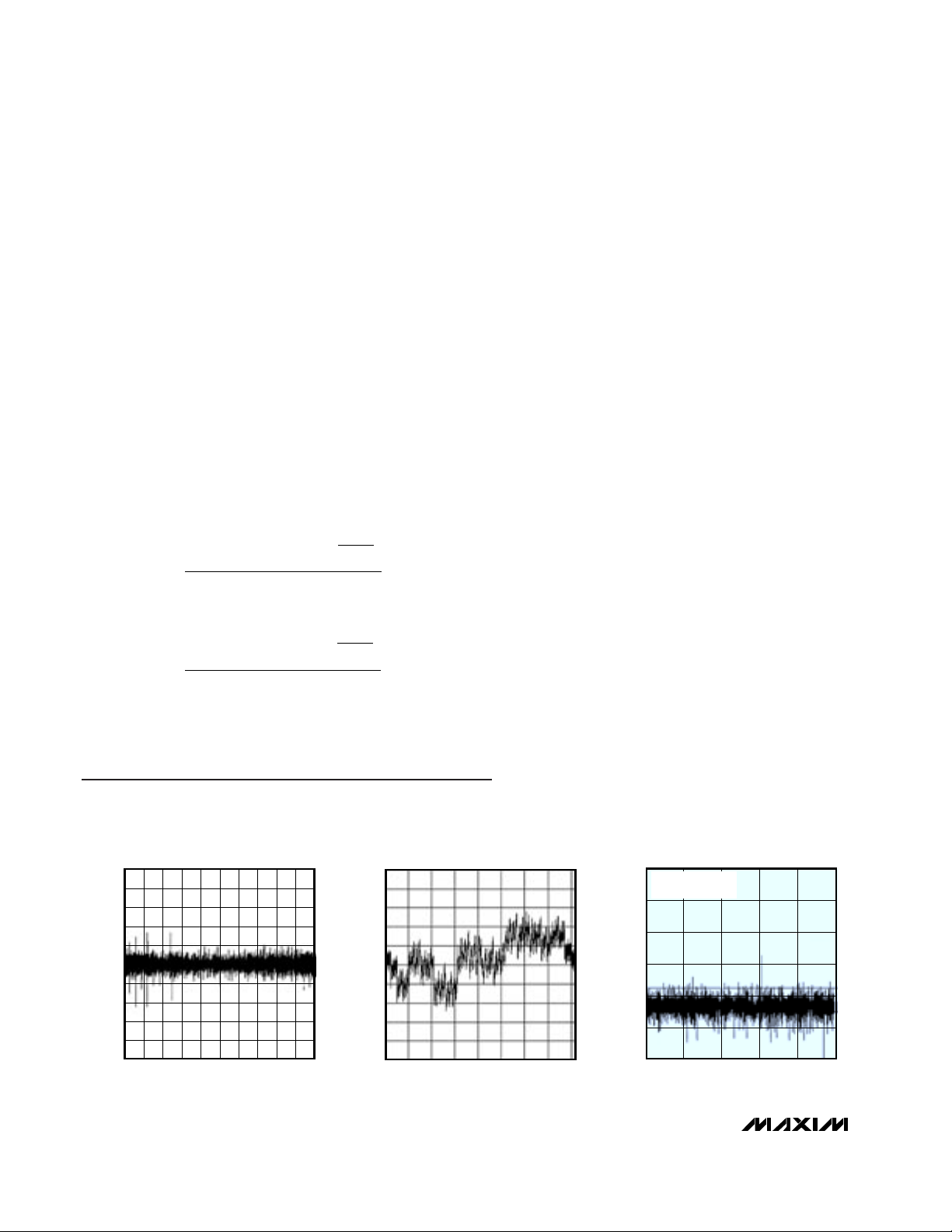
Typical Operating Characteristics
(VDD= 3.3V (MAX1363), VDD= 5V (MAX1364), f
SCL
= 1.7MHz, external clock, f
SAMPLE
= 94.4ksps, single-ended, unipolar,
T
A
= +25°C, unless otherwise noted.)
MAX1363/MAX1364
4-Channel, 12-Bit System Monitors with Programmable
Trip Window and SMBus Alert Response
6 _______________________________________________________________________________________
ELECTRICAL CHARACTERISTICS (continued)
(VDD= 2.7V to 3.6V (MAX1363), VDD= 4.5V to 5.5V (MAX1364), V
REF
= 2.048V (MAX1363), V
REF
= 4.096V (MAX1364), C
REF
=
0.1µF, f
SCL
= 1.7MHz, TA= T
MIN
to T
MAX
, unless otherwise noted. Typical values are at TA= +25°C.)
Note 1: Devices configured for unipolar single-ended inputs.
Note 2: Relative accuracy is the deviation of the analog value at any code from its theoretical value after the gain and offset have
been calibrated.
Note 3: Offset nulled.
Note 4: Conversion time is defined as the number of clock cycles needed for conversion multiplied by the clock period.
Conversion time does not include acquisition time. SCL is the conversion clock in the external clock mode.
Note 5: The throughput rate of the I
2
C bus is limited to 94.4ksps. The MAX1363/MAX1364 can perform conversions up to 133ksps
in monitor mode when not reading back results on the I
2
C bus.
Note 6: A filter on the SDA and SCL inputs suppresses noise spikes and delays the sampling instant.
Note 7: The absolute input-voltage range for the analog inputs (AIN0–AIN3) is from GND to V
DD
.
Note 8: When the internal reference is configured to be available at AIN3/REF (SEL[2:1] = 11), decouple AIN3/REF to GND with a
0.01µF capacitor.
Note 9: ADC performance is limited by the converter’s noise floor, typically 300µV
P-P
.
Note 10: Maximum conversion throughput in internal clock mode when the data is not clocked out.
Note 11: For the MAX1363, PSRR is measured as
and for the MAX1364, PSRR is measured as
Note 12: C
B
= total capacitance of one bus line in pF.
Note 13: f
SCLH
must meet the minimum clock low time plus the rise/fall times.
Note 14: A master device must provide a data hold time for SDA (referred to V
IL
of SCL) to bridge the undefined region of SCL’s
falling edge.
(
)
VVVV
(. ) (. )
36 27
FS FS
[]
−
VV
(. . )
36 27
−
N
21
−
×
V
REF
VVVV
(. ) (. )
55 45
FS FS
[]
−
VV
..
55 45
−
×
N
21
−
V
REF
DNL (LSB)
-0.1
-0.2
-0.3
-0.4
-0.5
DIFFERENTIAL NONLINEARITY
vs. DIGITAL CODE
0.5
0.4
0.3
0.2
0.1
0
1000 1500500
0 4000
2000 2500
DIGITAL OUTPUT CODE
3000 3500
MAX1363/64 toc01
1.0
0.8
0.6
0.4
0.2
INL (LSB)
-0.2
-0.4
-0.6
-0.8
-1.0
INTEGRAL NONLINEARITY
vs. DIGITAL CODE
0
1000 1500500
0 4000
2000 2500
DIGITAL OUTPUT CODE
3000 3500
MAX1363/64 toc02
FFT PLOT
-60
f
= 94.4ksps
SAMPLE
= 10kHz
f
IN
-80
-100
-120
AMPLITUDE (dBc)
-140
-160
-180
01020304050
FREQUENCY (kHz)
MAX1363/64 toc03
Page 7
MAX1363/MAX1364
4-Channel, 12-Bit System Monitors with Programmable
Trip Window and SMBus Alert Response
_______________________________________________________________________________________ 7
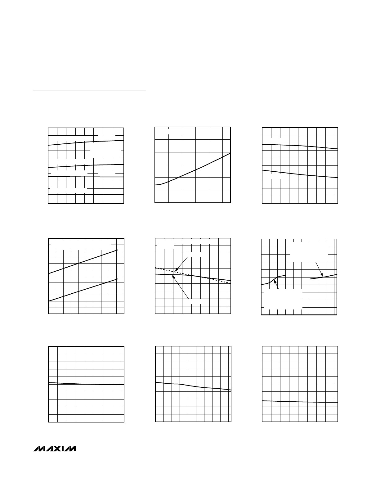
Typical Operating Characteristics (continued)
(VDD= 3.3V (MAX1363), VDD= 5V (MAX1364), f
SCL
= 1.7MHz, external clock, f
SAMPLE
= 94.4ksps, single-ended, unipolar,
T
A
= +25°C, unless otherwise noted.)
0
0.2
0.1
0.4
0.3
0.6
0.5
0.7
0.9
0.8
1.0
-40 -10 5-25 20 35 50 65 80
GAIN ERROR vs. TEMPERATURE
MAX1363/64 toc12
TEMPERATURE (°C)
GAIN ERROR (LSB)
SUPPLY CURRENT vs. TEMPERATURE
800
750
INTERNAL REFERENCE
700
650
600
INTERNAL REFERENCE
550
EXTERNAL REFERENCE
500
450
SUPPLY CURRENT (µA)
400
EXTERNAL REFERENCE
350
300
-40 -10 5-25 20 35 50 65 80
TEMPERATURE (°C)
MAX1364
SETUP BYTE
EXT REF: 10111010
INT REF: 11011010
MAX1363
MAX1364
MAX1363
AVERAGE SUPPLY CURRENT
vs. CONVERSION RATE (EXTERNAL CLOCK)
800
A) INTERNAL REFERENCE ALWAYS ON
750
B) EXTERNAL REFERENCE
700
650
600
(µA)
550
DD
500
450
AVERAGE I
400
350
300
250
200
010 50 70 90
02030406080100
CONVERSION RATE (ksps)
MAX1363/64 toc04
A
MAX1363/64 toc07
B
0.6
0.5
0.4
(µA)
0.3
DD
I
0.2
0.1
1.0010
1.0008
1.0006
1.0004
1.0002
1.0000
NORMALIZED
0.9998
REF
V
0.9996
0.9994
0.9992
0.9990
SHUTDOWN SUPPLY CURRENT
vs. SUPPLY VOLTAGE
SDA = SCL = V
0
2.7 5.2
DD
3.73.2 4.2 4.7
INPUT VOLTAGE (V)
INTERNAL REFERENCE VOLTAGE
vs. TEMPERATURE
NORMALIZED TO REFERENCE VALUE
AT +25°C
MAX1364
MAX1363
-40 -10 5-25 20 35 50 65 80
TEMPERATURE (°C)
MAX1363/64 toc05
1.00010
1.00008
1.00006
MAX1363/64 toc08
1.00004
1.00002
1.00000
NORMALIZED
0.99998
REF
V
0.99996
0.99994
0.99992
0.99990
SHUTDOWN SUPPLY CURRENT
vs. TEMPERATURE
0.50
0.45
MAX1364
0.40
0.35
0.30
0.25
0.20
MAX1363
0.15
SUPPLY CURRENT (µA)
0.10
0.05
0
-40 -10 5-25 20 35 50 65 80
TEMPERATURE (°C)
NORMALIZED REFERENCE VOLTAGE
vs. SUPPLY VOLTAGE
MAX1364
NORMALIZED TO
REFERENCE VALUE AT
= 5V
V
DD
MAX1363
NORMALIZED TO
REFERENCE VALUE AT
= 3.3V
V
DD
2.7 3.3 3.6 3.93.0 4.2 4.5 4.8 5.1 5.4
VDD (V)
MAX1363/64 toc06
MAX1363/64 toc09
OFFSET ERROR vs. TEMPERATURE
0
-0.1
-0.2
-0.3
-0.4
-0.5
-0.6
OFFSET ERROR (LSB)
-0.7
-0.8
-0.9
-1.0
-40 -10 5-25 20 35 50 65 80
TEMPERATURE (°C)
OFFSET ERROR vs. SUPPLY VOLTAGE
0
-0.1
MAX1363/64 toc10
-0.2
-0.3
-0.4
-0.5
-0.6
OFFSET ERROR (LSB)
-0.7
-0.8
-0.9
-1.0
2.7 3.3 3.6 3.93.0 4.2 4.5 4.8 5.1 5.4
VDD (V)
MAX1363/64 toc11
Page 8
MAX1363/MAX1364
4-Channel, 12-Bit System Monitors with Programmable
Trip Window and SMBus Alert Response
8 _______________________________________________________________________________________
Pin Description
Functional Diagram
Typical Operating Characteristics (continued)
(VDD= 3.3V (MAX1363), VDD= 5V (MAX1364), f
SCL
= 1.7MHz, external clock, f
SAMPLE
= 94.4ksps, single-ended, unipolar,
T
A
= +25°C, unless otherwise noted.)
GAIN ERROR vs. SUPPLY VOLTAGE
1.0
0.9
0.8
0.7
0.6
0.5
0.4
GAIN ERROR (LSB)
0.3
0.2
0.1
0
2.7 3.73.2 4.2 4.7 5.2
VDD (V)
MAX1363/64 toc13
MONITOR-MODE SUPPLY CURRENT
vs. SPEED
700
600
500
400
300
SUPPLY CURRENT (µA)
200
100
0
0 150
INTERNAL REF
EXTERNAL REF
SPEED (ksps)
MAX1363/64 toc14
125100755025
PIN NAME FUNCTION
1 AIN0 Analog Input
2 AIN1 Analog Input
3 AIN2 Analog Input
4 AIN3/V
REF
5A0I
Analog Input or Reference Input or Output. See Table 3.
2
C Address Select Input. Connect to VDD or GND. See Table 1.
6 INT Active-Low, Open-Drain Interrupt Output
7 SCL I2C Clock Input
8 SDA I2C Data Input/Output
9 GND Ground
10 V
DD
Positive Supply Voltage. Bypass V
to GND with a 0.1µF capacitor.
DD
V
DD
SDA
SCL
A0
INT
AIN0
AIN1
AIN2
AIN3/
REF
4:1
MUX
CLK
12-BIT
ADC
INT
REF
GND
I2C
INTERFACE
CONTROL
TRIP
THRESHOLDS
MAX1363/MAX1364
Page 9

Detailed Description
The MAX1363/MAX1364 4-channel ADCs use successive-approximation conversion techniques and fully differential input track/hold (T/H) circuitry to capture and
convert analog signals to a serial 12-bit digital output.
The MAX1363/MAX1364 feature a monitor mode with
programmable trip thresholds and window comparator.
The monitor function asserts an interrupt when any
channel violates the programmed upper or lower
thresholds. SMBus alert response allows the host
microcontroller (µC) to quickly identify which device
caused the interrupt. A programmable delay between
monitoring intervals lowers power consumption at lower
monitor rates.
The MAX1363/MAX1364 integrate an internal voltage
reference and clock. The software configures the analog inputs for unipolar/bipolar and single-ended/fully
differential operation. Integrated first-in/first-out (FIFO)
allows conversion of all channels, or eight conversions
on a selected channel to reduce interface overhead. An
I
2
C-compatible serial interface complies with standard,
fast, and high-speed (1.7MHz) modes.
MAX1363/MAX1364
4-Channel, 12-Bit System Monitors with Programmable
Trip Window and SMBus Alert Response
_______________________________________________________________________________________ 9
Figure 1a. F/S-Mode 2-Wire Serial-Interface Timing
Figure 2. Load Circuits
Figure 1b. HS-Mode 2-Wire Serial-Interface Timing
SDA
SCL
S
t
SU.STA
t
t
LOW
SU.DAT
t
HIGH
t
R
t
HD.DAT
t
F
SDA
t
t
LOW
SCL
t
HD.STA
Sr Sr
SU.DAT
1 9
t
HIGH
t
RCL
t
t
HD.DAT
FCL
t
SU.STA
t
SU.STA
t
R
t
HD.STA
t
HD.STA
ACK
Sr
ACK
t
SU.STO
9
PS
t
RDA
t
SU.STO
t
RCL1
t
F
t
BUF
t
FDA
P
S
HS-MODE
F/S-MODE
V
DD
I
OL
SDA
V
OUT
400pF
I
OH
Page 10

MAX1363/MAX1364
Power Supply
The MAX1363 (2.7V to 3.6V) and MAX1364 (4.5V to
5.5V) operate from a single supply and consume
670µA (typ) at sampling rates up to 94.4ksps and
436µA in monitor mode at 133ksps. The MAX1363
features a 2.048V internal reference, and the MAX1364
features a 4.096V internal reference. All devices can be
configured for use with an external reference from 1V to
VDD. Bypass VDDto GND using a 0.1µF or greater
ceramic capacitor for best performance.
Analog-Input and Track/Hold
The MAX1363/MAX1364 analog-input architecture contains an analog-input multiplexer (mux), fully differential
T/H, comparator, and a fully differential switched
capacitive digital-to-analog converter (DAC). Figure 3
shows the equivalent input circuit for the MAX1363/
MAX1364.
In single-ended mode, the analog-input mux connects
C
T/H
between the analog input selected by CS[3:0] and
GND (see the Configuration/Setup Bytes (Write Cycle)
section). In differential mode, the analog-input mux
connects C
T/H
to the plus and minus analog inputs
selected by CS[3:0].
During the acquisition interval, the T/H switches are in
the track position, and C
T/H
charges to the analog-input
signal. At the end of the acquisition interval, the T/H
switches move to the hold position, retaining the
charge on C
T/H
as a stable sample of the input signal.
During the conversion, a switched capacitive DAC
adjusts to restore the comparator input voltage to 0V
within the limits of 12-bit resolution. This action requires
12 conversion clock cycles and is equivalent to transferring a charge of 11pF x (VIN+ - VIN-) from C
T/H
to the
binary-weighted capacitive DAC, forming a digital representation of the analog-input signal.
Use a low source impedance to ensure an accurate
sample. A source impedance of up to 1.5kΩ does not
significantly degrade sampling accuracy. For larger
source impedances, connect a 100pF capacitor from
the analog input to GND or buffer the input.
In internal clock mode, the T/H circuitry enters track
mode on the eighth rising clock edge of the address
byte (see the Slave Address section). The T/H circuitry
enters hold mode on the falling clock edge of the
acknowledge bit of the address byte (the ninth clock
pulse). The conversions are then internally clocked, during which time the MAX1363/MAX1364 hold SCL low.
In external clock mode, the T/H circuitry enters track
mode after a valid address on the rising edge of the
clock during the read bit (R/W = 1). Hold mode is
entered on the rising edge of the second clock pulse
during the shifting out of the 1st byte of the result. The
next 12 clock cycles perform the conversions.
The time required for the T/H circuitry to acquire an
input signal is a function of the input sample capacitance. If the analog-input source impedance is high,
the acquisition time constant lengthens and more time
must be allowed between conversions. The acquisition
time (t
ACQ
) is the minimum time needed for the signal
to be acquired. It is calculated by:
t
ACQ
≥ 9 x (R
SOURCE
+ RIN) x C
IN
4-Channel, 12-Bit System Monitors with Programmable
Trip Window and SMBus Alert Response
10 ______________________________________________________________________________________
Figure 3. Equivalent Input Circuit
TRACK
TRACK
HOLD
TRACK
HOLD
C
HOLD
C
VDD/2
REF
REF
CAPACITIVE
DAC
CAPACITIVE
DAC
MAX1363
MAX1364
T/H
HOLD
TRACK
HOLD
TRACK
T/H
ANALOG-INPUT MUX
AIN0
AIN1
AIN2
AIN3/REF
GND
Page 11

where R
SOURCE
is the analog-input source impedance,
RIN= 2.5kΩ, and CIN= 22pF. For internal clock mode,
t
ACQ
= 1.5 / f
SCL
, and for external clock mode t
ACQ
=
2 / f
SCL
.
Analog-Input Bandwidth
The MAX1363/MAX1364 feature input-tracking circuitry
with a 5MHz small-signal bandwidth. The 5MHz input
bandwidth makes it possible to digitize high-speed
transient events and measure periodic signals with
bandwidths exceeding the ADC’s sampling rate by
using undersampling techniques. To avoid high-frequency signals from aliasing into the frequency band of
interest, use anti-aliasing filtering.
Analog-Input Range and Protection
Internal protection diodes clamp the analog inputs to V
DD
and GND. These diodes allow the analog inputs to swing
from (GND - 0.3V) to (VDD+ 0.3V) without causing damage to the device. For accurate conversions, the inputs
must remain within 50mV below GND or above V
DD
.
Single-Ended/Differential Input
The SE/DIF of the configuration byte configures the
MAX1363/MAX1364 analog-input circuitry for singleended or differential input. In single-ended mode (SE/DIF
= 1), the digital conversion results are the difference
between the analog input selected by CS[3:0] and GND.
In differential mode (SE/DIF = 0), the digital conversion
results are the difference between the plus and the minus
analog inputs selected by CS[3:0] (see Tables 5 and 6).
Unipolar/Bipolar
Unipolar mode sets the differential input range from 0
to V
REF
. A negative differential analog input in unipolar
mode causes the digital output code to be zero.
Selecting bipolar mode sets the differential input range
to ±V
REF
/ 2. The digital output code is binary in unipolar mode and two’s complement in bipolar mode. (See
the Transfer Functions section.)
In single-ended mode the MAX1363/MAX1364 always
operate in unipolar mode. The analog inputs are internally referenced to GND with a full-scale input range
from 0 to V
REF
(Table 7).
Reference
SEL[2:0] of the setup byte controls the reference and
the AIN3/REF configuration. When AIN3/REF is configured as a reference input or reference output (SEL1 =
1), differential conversions on AIN3/REF appear as if
AIN3/REF is connected to GND. A single-ended conversion in scan mode on AIN3/REF is ignored by an internal
limiter that sets the highest available channel at AIN2.
Internal Reference
The internal reference is 2.048V for the MAX1363 and
4.096V for the MAX1364. SEL1 of the setup byte controls whether AIN3/REF is used for an analog input or a
reference. Decouple AIN3/REF to GND with a 0.1µF
capacitor and a 2kΩ resistor in series with the capacitor. When AIN3/REF is configured as an internal reference output (SEL[1:0] = 11). See the Typical Operating
Circuit. Once powered up, the reference remains on
until reconfigured. Do not use the reference to supply
current for external circuitry.
External Reference
The external reference ranges from 1V to V
DD
. For maximum conversion accuracy, the reference must deliver
40µA and have an impedance of 500Ω or less. For
noisy or high-output-impedance references, insert a
0.1µF bypass capacitor to GND as close to AIN3/REF
as possible.
Clock Modes
The clock mode determines the conversion clock and
the data acquisition and conversion time. The clock
mode also affects the scan mode. The state of the
setup byte’s INT/EXT clock bit determines the clock
mode. At power-up, the MAX1363/MAX1364 default to
internal clock mode (INT/EXT clock = 0).
Internal Clock
See the Configuration/Setup Bytes (Write Cycle) section.
In internal clock mode (CLK = 0), the MAX1363/
MAX1364 use an internal oscillator for the conversion
clock. The MAX1363/MAX1364 begin tracking the analog
input after a valid address on the eighth rising edge of the
clock. On the falling edge of the ninth clock, the analog
signal is acquired and the conversion begins. While converting, the MAX1363/MAX1364 hold SCL low (clock
stretching). After completing the conversion, the results
are stored in internal memory. For scan-mode configurations with multiple conversions (see the Scan Modes section), all conversions happen in succession with each
additional result stored in memory. Once all conversions
are complete, the MAX1363/MAX1364 release SCL,
allowing it to go high. The master can now clock the
results out in the same order as the scan conversion.
The converted results are read back in a FIFO
sequence. If AIN3/REF is configured as a reference
input or output, AIN3/REF is excluded from multichannel scan. If reading continues past the final result
stored in memory, the pointer wraps around and points
to the first result. Only the current conversion results
are read from memory. The MAX1363/MAX1364 must
be addressed with a read command to obtain new conversion results.
MAX1363/MAX1364
4-Channel, 12-Bit System Monitors with Programmable
Trip Window and SMBus Alert Response
______________________________________________________________________________________ 11
Page 12

MAX1363/MAX1364
External Clock
See the Configuration/Setup Bytes (Write Cycle) section.
When configured for external clock mode (CLK = 1), the
MAX1363/MAX1364 use SCL as the conversion clock. In
external clock mode, the MAX1363/MAX1364 begin
tracking the analog input on the ninth rising clock edge of
a valid slave address byte. Two SCL clock cycles later,
the analog signal is acquired and the conversion begins.
Unlike internal clock mode, converted data is clocked out
immediately in the format described in the Reading a
Conversion (Read Cycle) section.
The device continuously converts input channels dictated by the scan mode until given a not acknowledge
(NACK). There is no need to readdress the device with
a read command to obtain new conversion results.
The conversion must complete in 1ms or droop on the
T/H capacitor degrades conversion results. Use internal clock mode if the SCL clock period exceeds 60µs.
Use external clock mode for conversion rates from
40ksps to 94.4ksps. Use internal clock mode for conversions under 40ksps. Internal clock mode consumes less
power. Monitor mode always uses internal clock mode.
Applications Section
Power-On Reset
The configuration and setup registers default to a single-ended, unipolar, single-channel conversion on
AIN0 using the internal clock with VDDas the reference
and AIN3/REF configured as an analog input. The
memory contents are unknown at power-up (see the
Software Description section).
I2C-Compatible 2-Wire Serial Interface
The MAX1363/MAX1364 use an I2C-compatible 2-wire
interface consisting of a serial data line (SDA) and serial
clock line (SCL). SDA and SCL facilitate bidirectional
communication between the MAX1363/MAX1364 and
the master at rates up to 1.7MHz. The master (typically
a µC) initiates data transfer on the bus and generates
the SCL signal to permit data transfer. The MAX1363/
MAX1364 behave as I2C slave devices that transfer and
receive data.
SDA and SCL must be pulled high for proper I2C operation. This is typically done with pullup resistors (750Ω
or greater). Series resistors (RS) are optional (see the
Typical Operating Circuit section). The resistors protect
the input architecture of the MAX1363/MAX1364 from
high voltage spikes on the bus lines and minimize
crosstalk and undershoot of the bus signals.
One bit transfers during each SCL clock cycle. A minimum of nine clock cycles is required to transfer a byte
in or out of the MAX1363/MAX1364 (8 bits and an
ACK/NACK). The data on SDA must remain stable during the high period of the SCL clock pulse. Changes in
SDA while SCL is stable and high are considered control signals (see the START and STOP Conditions section). Both SDA and SCL remain high when the bus is
not busy.
START and STOP Conditions
The master initiates a transmission with a START condition (S), which is a high-to-low transition on SDA while
SCL is high. The master terminates a transmission with
a STOP condition (P), which is a low-to-high transition
on SDA while SCL is high (Figure 4). A repeated START
condition (Sr) can be used in place of a STOP condition
to leave the bus active and the mode unchanged (see
the HS I
2
C Mode section).
Acknowledge and Not-Acknowledge Conditions
Data transfers are framed with an acknowledge bit
(ACK) or a not-acknowledge bit (NACK). Both the master and the MAX1363/MAX1364 (slave) generate
acknowledge bits. To generate an acknowledge, the
receiving device must pull SDA low before the rising
edge of the acknowledge-related clock pulse (ninth
pulse) and keep it low during the high period of the
clock pulse (Figure 5).
To generate a not-acknowledge condition, the receiver
allows SDA to be pulled high before the rising edge of
the acknowledge-related clock pulse, and leaves SDA
high during the high period of the clock pulse.
Monitoring the acknowledge bits allows for detection of
4-Channel, 12-Bit System Monitors with Programmable
Trip Window and SMBus Alert Response
12 ______________________________________________________________________________________
Figure 4. START and STOP Conditions
Figure 5. Acknowledge Bits
SP
SDA
SCL
S
SDA
SCL
12 89
Sr
NOT ACKNOWLEDGE
ACKNOWLEDGE
Page 13

unsuccessful data transfers. An unsuccessful data transfer happens if a receiving device is busy or if a system
fault has occurred. In the event of an unsuccessful data
transfer, the bus master reattempts communication at a
later time.
Slave Address
The MAX1363/MAX1364 have a 7-bit I2C slave
address. The slave address is selected using A0. The
MAX1363/MAX1364 (EUB, MEUB, and LEUB) have
three base address options, allowing up to six devices
concurrently per I2C bus (see Table 1).
The MAX1363/MAX1364 continuously wait for a START
condition followed by its slave address. When the device
recognizes its slave address, it is ready to accept or
send data depending on the R/W bit (Figure 6).
HS I2C Mode
At power-up, the MAX1363/MAX1364 bus timing is set
for fast mode (F/S mode, up to 400kHz I2C clock), which
limits the conversion rate to approximately 22ksps.
Switch to high-speed mode (HS mode, up to 1.7MHz
I2C clock) to achieve conversion rates up to 94.4ksps.
The MAX1363/MAX1364 convert up to 133ksps in monitor mode, regardless of I2C mode. If conversion results
are unread, I2C bandwidth limitations do not apply (see
the Monitor Mode section).
Select HS mode by addressing all devices on the bus
with the HS-mode master code 0000 1XXX (X = don’t
care). After successfully receiving the HS-mode master
code, the MAX1363/MAX1364 issue a NACK, allowing
SDA to be pulled high for one clock cycle (Figure 7).
After the NACK, the MAX1363/MAX1364 operate in HS
mode. Send a repeated START (Sr) followed by a slave
address to initiate HS-mode communication. If the master generates a STOP condition, the MAX1363/
MAX1364 return to F/S mode. Use a repeated START
condition (Sr) in place of a STOP condition to leave the
bus active and the mode unchanged.
MAX1363/MAX1364
4-Channel, 12-Bit System Monitors with Programmable
Trip Window and SMBus Alert Response
______________________________________________________________________________________ 13
Figure 6. MAX1363/MAX1364 Slave Address Byte
Table 1. I2C Slave Selection Table
Figure 7. F/S-Mode to HS-Mode Transfer
SLAVE ADDRESS
011 1000R/W ACK
S
SDA
SCL
A0 STATE SUFFIX ADDRESS
Low EUB 0110100
High EUB 0110101
Low LEUB 0110010
High LEUB 0110011
Low MEUB 0110110
High MEUB 0110111
123456789
000 10XXXNACK
S Sr
SDA
SCL
HS-MODE MASTER CODE
F/S MODE HS MODE
Page 14

MAX1363/MAX1364
4-Channel, 12-Bit System Monitors with Programmable
Trip Window and SMBus Alert Response
14 ______________________________________________________________________________________
Figure 8. Example of Writing Setup and Control Bytes
Figure 9. Example of Extended Setup Byte Writing
Table 2. Configuration Byte Format*
*Power-on defaults: 0x01
START
CONDITION
START
ADDRESS
FROM THE MASTER
R/W BIT FROM
THE MASTER
0A AASTOP
CONFIGURATION
BYTE FROM THE MASTER
START
CONDITION
START
CH 0 LT [11:4] BYTE
BIT NAME DESCRIPTION
ADDRESS
FROM THE MASTER
R/W BIT FROM
THE MASTER
0A 1A A
CH 0 LT [3:0];
UT [11:8] BYTE
SETUP BYTE
FROM THE MASTER
7(MSB) CONFIG The configuration byte always starts with 0.
6 SCAN1
5 SCAN0
4 CS3
3 CS2
2 CS1
SCAN1, SCAN0 = [0,0], scans from channel 0 to the upper channel chosen by CS1, CS0.
SCAN1, SCAN0 = [0,1], converts a single channel chosen by CS1, CS0 eight times.
SCAN1, SCAN0 = [1,0] monitor mode monitors from channel 0 to the upper channel chosen by CS1, CS0.
SCAN1, SCAN0 = [1,1], single channel conversion for the channel is chosen by CS0, CS1.
CS3, CS2 = [1,1] enables readback of monitor-mode setup data.
Selects the upper limit of the channel range used for the conversion sequence in scan modes SCAN = [0,0]
and monitor modes SCAN = [1,0].
1 CS0
Selects the conversion channel when SCAN = [0,1] or when SCAN = [1,1].
(Tables 5 and 6)
SETUP
BYTE FROM THE MASTER
ALARM RESET, SCAN
SPEED, BYTE FROM MASTER
CH 1 LT [11:4] BYTECH 0 UT [7:0] BYTEAAAASTOP
1 = single-ended inputs.
0 = differential inputs.
AIN0 and AIN1 form the first differential pair and AIN2 and AIN3 form the second differential pair. (See Tables
4 and 5.)
0 SE/DIF
Selects single-ended or differential conversions. In single-ended mode, input-signal voltages are referenced
to GND. In differential mode, the voltage difference between two channels is measured.
When single-ended mode is used, the MAX1363/MAX1364 perform unipolar conversions regardless of the
UNI/BIP bit in the setup byte.
(Table 7)
Page 15
Software Description
Configuration/Setup Bytes (Write Cycle)
A write cycle begins with the bus master issuing a
START condition followed by 7 address bits and a write
bit (R/W = 0). If the address byte is successfully
received, the MAX1363/MAX1364 (slave) issue an
ACK. The master then writes to the slave. If the most
significant bit (MSB) is 1, the slave recognizes the
received byte as the setup byte (Table 4). If the MSB is
0, the slave recognizes that byte as the configuration
byte (Table 2). Write to the configuration byte before
writing to the setup byte (Figure 8). If enabling RESET
in the setup byte, rewrite the configuration byte after
writing the setup byte, since RESET clears the contents
of the configuration byte back to the power-up state.
When the monitor-setup bit of the setup byte is set to 1,
writing extends up to 13 bytes to clock in monitor-setup
data. Terminate writing monitor-setup data at any time
by issuing a STOP or repeated START condition. If the
slave receives a byte successfully, it issues an ACK
(Figure 9).
Note: When operating in HS mode, a STOP condition
returns the bus into F/S mode (see the HS I
2
C Mode
section).
Automatic Shutdown
AutoShutdown occurs between conversions when the
MAX1363/MAX1364 are idle. When operating in external clock mode, issue a STOP, NACK, or repeated
START condition to place the devices in idle mode and
benefit from automatic shutdown. A STOP condition is
not necessary in internal clock mode for automatic
shutdown because power-down occurs once all contents are written memory. Shutdown reduces supply
current to less than 0.5µA (external reference mode,
typ) and 300µA (internal reference mode, typ).
When idle, the MAX1363/MAX1364 continuously wait
for a START condition followed by their slave address.
Upon reading a valid address byte, the MAX1363/
MAX1364 power up. The internal reference requires
10ms to wake up. Therefore, power up the internal reference 10ms prior to conversion or leave the reference
continuously powered. Wake-up is transparent when
using an external reference or V
DD
as the reference.
Automatic shutdown results in dramatic power savings,
particularly at slow conversion rates with internal clock.
For example, using an external reference at a conversion rate of 10ksps, the average supply current for the
MAX1363 is 60µA (typ) and drops to 6µA (typ) at
1ksps. At 0.1ksps, the average supply current is just
1µA. Table 3 shows AIN3/REF configuration and reference power-down state.
Scan Modes
SCAN1 and SCAN0 of the configuration byte set the
scan-mode configuration. When configuring AIN3/REF
for reference input or output (SEL0 = 1), AIN3/REF is
excluded from a multichannel scan. The scanned
results write to memory in the same order as the conversion. Start a conversion sequence by initiating a
read with the desired scan mode. Read the results from
memory in the order they were converted (see the
Reading a Conversion (Read Cycle) section).
Selecting channel scan mode [0,0] starts converting
from channel 0 up to the channel chosen by CS1, CS0.
Selecting channel scan mode [0,1] converts the channel selected by CS1, CS0 eight times and returns eight
consecutive results.
Selecting monitor mode [1,0] initiates a continuous conversion scan sequence from channel 0 to the channel
selected by CS1, CS0. See the Monitor Mode section
for more details.
Selecting channel scan mode [1,1] performs a single
conversion on the channel selected by CS1, CS0 and
returns the result.
Reading a Conversion (Read Cycle)
Initiate a read cycle to start a conversion sequence and
to obtain conversion results. See the Scan Modes
section for details on the channel-scan sequence. Read
MAX1363/MAX1364
4-Channel, 12-Bit System Monitors with Programmable
Trip Window and SMBus Alert Response
______________________________________________________________________________________ 15
Table 3. Reference Voltage and AIN3/REF Format
SEL1 SEL0
00 X V
01 X External reference Reference input Always off
10 0 Internal reference Analog input Always off
10 1 Internal reference Analog input Always on
11 0 Internal reference Reference output Always off
11 1 Internal reference Reference output Always on
INT REF
POWER-DOWN
REFERENCE VOLTAGE AIN3/REF
DD
Analog input Always off
REFERENCE STATE
INTERNAL
Page 16
MAX1363/MAX1364
cycles begin with the bus master issuing a START
condition followed by 7 address bits and a read bit
(R/W = 1). After successfully receiving the address byte,
the MAX1363/MAX1364 (slave) issue an ACK. The master
then reads from the slave. (See Figures 10–13.)
The result is transmitted in 2 bytes. The 1st byte consists of a leading 1 followed by a 2-bit binary channel
address tag, a 12/10 bit flag (1 for the MAX1363/
MAX1364), the first 4 bits of the data result, and the
expected ACK from the master. The 2nd byte contains
D7–D0. To read the next conversion result, issue an
ACK. To stop reading, issue a NACK.
4-Channel, 12-Bit System Monitors with Programmable
Trip Window and SMBus Alert Response
16 ______________________________________________________________________________________
Table 4. Setup-Byte Format*
*Power-on defaults: 0x82
Table 5. Channel Selection in SingleEnded Mode (SE/DIF = 1)
Table 6. Channel Selection in Differential
Mode (SE/DIF = 0)
Table 7. SE/DIF and UNI/BIP Table
BIT NAME DESCRIPTION
7 (MSB) Setup Setup byte always starts with 1.
6 REF/AIN SEL1
5 REF/AIN SEL0
4
3 INT/EXT Clock
2 UNI/BIP
INT REF Power
Down
1 Reset
0 Monitor Setup
When [0,0], REF/AIN3 = AIN3, REF = V
When [0,1], REF/AIN3 = REF, apply external reference to REF.
When [1,0], REF/AIN3 = AIN3, REF = internal reference.
When [1,1], REF/AIN3 = REF, REF = internal reference.
(Table 3)
1 = internal reference always powered up.
0 = internal reference always powered down.
(Table 3)
0 = internal clock.
1 = external clock (MAX1363/MAX1364 use the SCL clock for conversions).
0 = unipolar.
1 = bipolar.
Selects unipolar or bipolar conversion mode. In unipolar mode, analog signal in 0 to V
be converted. In differential bipolar mode, input signal can range from -V
single-ended mode is chosen, the SE/DIF bit of configuration byte overrides UNI/BIP, and
conversions are performed in unipolar mode.
1 = no action.
0 = resets INT and configuration register. Setup register and channel trip thresholds are unaffected.
0 = no action.
1 = extends writing up to 13 bytes (104 bits) of alarm reset mask. Scans speed selection and alarm
thresholds. See the Configuring Monitor Mode section.
DD.
REF
/ 2 to +V
REF
REF
range can
/ 2. When
CS1 CS0 CH0 CH1 CH2 CH3
00+
01 +
10 +
11 +
CS1 CS0 CH0 CH1 CH2 CH3
00+01-+
10 +11 -+
SE/DIF UNI/BIP MODE
00Differential inputs, unipolar
01Differential inputs, bipolar
10Single-ended inputs, unipolar
11Single-ended inputs, unipolar
Page 17

MAX1363/MAX1364
4-Channel, 12-Bit System Monitors with Programmable
______________________________________________________________________________________ 17
Table 8. Data Format
Figure 10. Example of Reading the Conversion Result—External Clock Mode
Figure 11. Example of a Single Conversion Using the Internal Clock, SCAN = 1,1
Figure 12. Example of Scan-Mode Conversions Using the Internal Clock, SCAN = 0,0 and 0,1
HIGH CH1 CH0 12/11110000HIGH HIGH
1 0/1 0/1
0 = 10b
1 = 12b
START
CONDITION
START
110/1 0/1 ACK 0/1 0/1 0/1 0/1 0/1 0/1 0/1 0/1
ADDRESS
FROM THE MASTER
DATA
(MSB)
R/W
1 ACK ACK ACK STOP
D8 D7 D6 D5 D4 D3 D2 D1 D0
1, CH ADD, 10b/12b FLAG,
RESULT (4 MSBs)
t
ACQ
t
CONV
R/W
START
ADDRESS
FROM THE MASTER
1 ACK
t
ACQ
MAX1363/MAX1364
KEEPS SCL LOW
6.8µs MAX
t
CONV
1, CH ADD, 10b/12b,
RESULT (4 MSBs)
R/W
START
ADDRESS
FROM THE MASTER
1 ACK
t
ACQ
CONVERSION 1
t
CONV
6.8µs MAX
MAX1363/MAX1364
KEEPS SCL LOW
RESULT (8 LSBs)
ACK
t
ACQ
RESULT (8 LSBs)
CONVERSION 2
t
CONV
ACK/
NACK
ACK STOP
MAX1363/MAX1364
KEEPS SCL LOW
t
ACQ
CONVERSION N
t
CONV
1, CH ADD, 10b/12b,
RESULT (4 MSBs)
1, CH ADD, 10b/12b,
RESULT (4 MSBs)
RESULT N
(8 LSBs)
RESULT 1
(8 LSBs)
ACK
ACKACK
STOPACK
Page 18

MAX1363/MAX1364
When the MAX1363/MAX1364 receive a NACK, they
release SDA allowing the master to generate a STOP or
a repeated START condition.
Monitor Mode
Monitor-Mode Overview
The MAX1363/MAX1364 automatically monitor up to four
input channels. For systems with limited I2C bandwidth,
monitor mode allows the µC to set a window by
programming lower and upper thresholds during initialization, and only intervening if the MAX1363/MAX1364
detect an alarm condition. This allows an interrupt-driven
approach as an alternative to continuously polling the
ADC with the µC. Monitor mode reduces processor overhead and conserves I2C bandwidth.
The following shows an example of events in
monitor mode:
1) Fault condition(s) detected, INT asserted.
2) Host µC services interrupt and sends SMBus alert to
identify the alarming device. The MAX1363/
MAX1364 respond with the I
2
C slave address, pend-
ing arbitration rules. (See the SMBus Alert section.)
3) The MAX1363/MAX1364 release the INT.
4) Host µC reads the alarm-status register, latchedfault register, and current-conversion results to
determine the alarming channel(s) and course
of action.
5) Host µC services alarm(s); adjusts system parameters as needed and/or adjusts lower and upper
thresholds.
6) Host µC resets the alarming channel. See the
Configuring Monitor Mode section.
7) Monitor mode resumes.
8) If there is still an active fault, the device asserts INT
again. See step 1.
Writing SCAN1 and SCAN0 bits = [1,0] in the configuration byte activates monitor mode. The MAX1363/
MAX1364 scan from channels 0 up to the channel
selected by [CS1:CS0] at a rate determined by the
scan delay bits. The MAX1363/MAX1364 compare the
conversion results with the lower and upper thresholds
for each channel. When any conversion exceeds the
threshold, the MAX1363/MAX1364 assert an interrupt
by pulling INT low (if enabled). The MAX1363/
MAX1364 set the corresponding flag bit in the alarmstatus register and write conversion results to the
latched-fault register to record the event causing the
alarm condition.
INT active state is randomly delayed with respect to the
conversion. Depending on the number of channels
scanned and the position in the channel scan sequence,
the maximum possible delay for asserting INT is five
conversion periods (37.5µs typ, Delay = 0,0,0).
Configuring Monitor Mode
To write monitoring setup data, set the monitor-setup bit
(bit 0 in setup byte) to 1 to extend writing up to 104 bits
(13 bytes) of monitoring setup data. The number of bits
written to the MAX1363/MAX1364 depends on whether
the part is in single-ended or differential mode and
whether the upper channel limit is set by [CS1:CS0]
(Table 9).
Terminate writing at any time by using a STOP or
repeated START condition. Previous monitoring setup
data not overwritten remains valid.
A 1 written to the reset alarm CH_ clears the alarm, otherwise no action occurs (Table 10). Deassert INT by
4-Channel, 12-Bit System Monitors with Programmable
Trip Window and SMBus Alert Response
18 ______________________________________________________________________________________
Figure 13. Example of Scan-Mode Conversions Using the External Clock, SCAN = 0,0 and 0,1
START
ADDRESS
FROM THE MASTER
1, CH ADD, 10b/12b,
RESULT (4 MSBs)
t
ACQ
1 ACK ACK ACK
ACK ACK
1, CH ADD, 10b/12b
t
ACQ
RESULT N (8 LSBs)
CONVERSION N
RESULT (4 MSBs)
CONVERSION 1
t
ACQ
RESULT (8 LSBs)
t
ACQ
Page 19

clearing all alarms or by initiating an SMBus alert during an alarm condition (see the SMBus Alert section).
The Delay 2, Delay 1, Delay 0 bits set the speed of
monitoring by changing the delay between conversions. Delay 2, 1, 0 = 000 sets the maximum possible
speed; 001 divides the maximum speed by ~2.
Increasing delay values further divides the previous
speed by two.
INT_EN controls the open-drain INT output. Set INT_EN
to 1 to enable the hardware interrupt. Set INT_EN to 0
to disable the hardware interrupt output. The INT output
tri-states when disabled or when there are no alarms.
The master can also poll the alarm status register at
any time to check the alarm status.
Repeat clocking channel threshold data up to the channel programmed by CS1 and CS0 (Table 12). For differential input mode, omit odd channels; the lower and
upper threshold data applies to channel pairs. There is
no need to clock in dummy data for odd (or even)
channels (Table 6).
To disable alarming on a specific channel, set the lower
threshold to 0x800 and the upper threshold to 0x7FF for
MAX1363/MAX1364
4-Channel, 12-Bit System Monitors with Programmable
Trip Window and SMBus Alert Response
______________________________________________________________________________________ 19
Table 9. Monitor-Mode Setup Data Format
Table 10. Alarm Reset, Scan Speed Register, and INT_EN Data Format
Table 11. Delay Settings
*When using delay = [0,0,0] in internal reference mode and
AIN3/REF configured as a REF output, the MAX1363/MAX1364
may exhibit a code-dependent gain error due to insufficient
internal reference drive. Gain error caused by this phenomenon
is typically less than 1%FSR (0.1µF C
REF
) and increases with a
larger C
REF
. Avoid this gain error by using an external reference,
V
DD
, as a reference or use an internal reference with AIN3/REF
as an analog input (see Table 4). Alternatively, choose delay bits
other than [0,0,0] to lower the conversion rate.
Table 12. Lower and Upper Threshold Data Format
X = Don’t care.
ACK = Acknowledge.
Alarm reset, scan
speed, INT_EN ,
(8 bits)
RESET
ALARM CH 0
0/1 0/1 0/1 0/1 0/1 0/1 0/1 0/1
AIN0 thresholds
(24 bits)
RESET
ALARM CH 1
RESET
ALARM CH 2
DELAY 2 DELAY 1 DELAY 0
000 133.0*
001 66.5
010 33.3
011 16.6
100 8.3
101 4.2
110 2.0
111 1.0
CONVERSION RATE
AIN1 thresholds
(skip if differential mode, or
CS1, CS0 < 1) (24 bits)
RESET
ALARM CH 3
MONITOR-MODE
(ksps)
AIN2 thresholds (skip if
CS1, CS0 < 2)
(24 bits)
DELAY 2 DELAY 1 DELAY 0 INT_EN
AIN3 thresholds (skip if differential
mode, or CS1, CS0 < 3)
(24 bits)
BYTE B7 B6 B5 B4 B3 B2 B1 B0 ACKNOWLEDGE
1
2 LT3 LT2 LT1 LT0 (LSB)
3 UT7 UT6 UT5 UT4 UT3 UT2 UT1 UT0 (LSB) ACK
LT11
(MSB)
LT10 LT9 LT8 LT7 LT6 LT5 LT4 ACK
UT11
(MSB)
UT10 UT9 UT8 ACK
Page 20
MAX1363/MAX1364
bipolar mode, or set the lower threshold to 0x000 and
the upper threshold to 0xFFF for unipolar mode.
Readback Mode
Select readback mode by setting CS3, CS2 to [1,1] in
the configuration byte. Begin a read operation to start
reading back monitor-setup data. Clock out delay bit
settings, INT_EN bit, and the lower and upper thresholds programmed for each channel. Readback mode
follows exactly the same format as writing to the monitor-setup data, with the exception of the first 4 alarmreset bits, which are always 1 (Table 13).
Reading in Monitor Mode
Reading in monitor mode reads back the alarm-status
register, latched-fault register, and current-conversion
results as shown in Table 14.
The MAX1363/MAX1364 register pointer loops back to
the beginning of the current-conversion result after
reading the last conversion result. Stop reading at any
time by asserting a STOP condition or NACK.
Note: The MAX1363/MAX1364 do not update the current-conversion results register while reading in monitor
mode. Monitor mode resumes after a STOP condition or
NACK.
Alarm-Status Register and Latched-Fault Register
The latched-fault register records a snapshot of the
alarming channel at the instance that a fault condition is
asserted. An alarm-status bit of 1 (Table 15) indicates a
fault, and the data in the latched-fault register of the
corresponding channel contains the conversion result
that caused the alarm to trip. Resetting alarms does not
clear the latched-fault register, thus the latched-fault
register contains valid data only if an alarm status bit is
high for the given channel.
The current-conversion register contains the most
recent conversion results. If the user attempts to read
past the last result of the current-conversion register,
the MAX1363/MAX1364 wraps back to the beginning of
the current-conversion result.
The latched-fault register and current-conversion register follow the data format in the Reading a Conversion
(Read Cycle) section. Register length depends on the
number of conversions in one monitoring sequence. For
example, when channel pairs 0/1 and channels 2/3 are
monitored differentially, there are only two conversion
results to report. The latched-fault register is 2 x 16 bits
long, after which two current-conversion results follow.
Likewise, if CS0 and CS1 limit the upper bound of the
channel scan range from CH0 to CH2 in single-ended
mode, the latched-fault register clocks out 3 x 16 bits of
data followed by the current-conversion results, also 3 x
16 bits.
4-Channel, 12-Bit System Monitors with Programmable
Trip Window and SMBus Alert Response
20 ______________________________________________________________________________________
Table 13. Readback-Mode Format
Table 14. Reading in Monitor-Mode Data Format
Table 15. Alarm-Status Register
0 = Not-alarm condition.
1 = Alarm condition.
Table 16. Latched-Fault and CurrentConversion Register
ALARM RESET/SCAN SPEED
1111D2 D1 D0 INT 24 bits 24 bits 24 bits 24 bits
ALARM-STATUS REGISTER LATCHED-FAULT REGISTER CURRENT-CONVERSION RESULTS
8 bits 16, 32, 48, or 64 bits 16, 32, 48, or 64 bits
CH0 UP CH0 LOW CH1 UP CH1 LOW CH2 UP CH2 LOW CH3 UP CH3 LOW
0/1 0/1 0/1 0/1 0/1 0/1 0/1 0/1
AIN0
THRESHOLDS
AIN0 AIN1 AIN2 AIN3
16-bit read 16-bit read 16-bit read 16-bit read
AIN1 THRESHOLDS
(SKIP IF DIFFERENTIAL
MODE OR CS1, CS0 < 1)
AIN2 THRESHOLDS
(SKIP IF CS1, CS0 < 2)
AIN3 THRESHOLDS
(SKIP IF DIFFERENTIAL
MODE OR CS1, CS0 < 3)
Page 21
Resetting Alarm
Reset alarms by writing to monitor-setup data. See the
Configuring Monitor Mode section and Table 10.
SMBus Alert
The SMBus-alert feature provides a quick method to
identify alarming devices on a shared interrupt. Upon
receiving an interrupt signal, the host µC can broadcast
a receive byte request to the alert-response slave
address (0001100). Any slave device that generated an
interrupt attempts to identify itself by putting its own
address on the bus. The alert response can activate
several different slave devices simultaneously. If more
than one slave attempts to respond, bus arbitration
rules apply, and the device with the lower address wins
as a consequence of the open-collector bus. The losing
device does not generate an acknowledgement and
continues to hold the alert line low until serviced.
Successful reading of the alert response address deasserts INT.
When the MAX1363/MAX1364 successfully send the
I
2
C address, it can resume and reassert INT right away
(if the fault is still present). To prevent this from happening, monitor mode does not resume until after the host
controller resets the alarm in the alarm status register.
Any alarms not cleared when the device resumes monitor mode reassert INT.
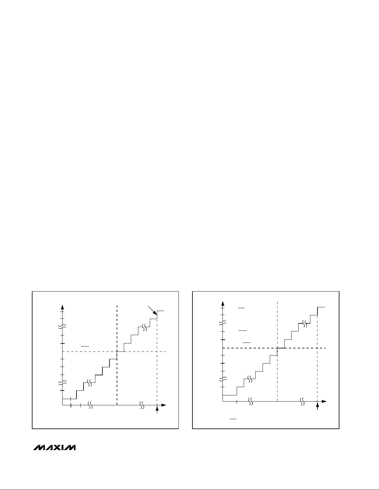
Transfer Functions
Output data coding for the MAX1363/MAX1364 is binary in unipolar mode and two’s complement in bipolar
mode with 1 LSB = V
REF
/ 2N, where N is the number of
bits. Code transitions occur halfway between successive-integer LSB values. Figures 14 and 15 show the
transfer functions for unipolar and bipolar operations,
respectively.
Layout, Grounding, and Bypassing
Only use PC boards. Wire-wrap configurations are not
recommended since the layout should ensure proper
separation of analog and digital traces. Do not run analog and digital lines parallel to each other, and do not
layout digital signal paths underneath the ADC package. Use separate analog and digital PC board ground
sections with only one star point (Figure 16).
High-frequency noise in the power supply (VDD) could
influence the proper operation of the ADC’s fast comparator. Bypass VDDto the star ground with a network
of two parallel capacitors, 0.1µF and 4.7µF, located as
close as possible to the MAX1363/MAX1364 power supply. Minimize capacitor lead length for best supply noise
rejection. For extremely noisy supplies, add an attenuation resistor (5Ω) in series with the power supply.
MAX1363/MAX1364
4-Channel, 12-Bit System Monitors with Programmable
Trip Window and SMBus Alert Response
______________________________________________________________________________________ 21
Figure 14. Unipolar Transfer Function
Figure 15. Bipolar Transfer Function
OUTPUT CODE
111...111
111...110
100...010
100...001
100...000
011...111
011...110
011...101
000...001
000...000
FS = REF + GND
ZS = GND
V
REF
1 LSB =
1024
0
1
INPUT VOLTAGE (LSB)(GND)
512
FULL-SCALE
TRANSITION
FS - 0.5 LSB
OUTPUT CODE
V
REF
FS =
011...111
011...110
000...010
000...001
000...000
111...111
111...110
111...101
100...001
100...000
-FS + 0.5 LSB
AIN- ≥
2
2
ZS = AIN-
-V
REF
-FS =
2
1 LSB =
1024
V
REF
+ AIN-
+ AIN-
V
REF
INPUT VOLTAGE (LSB)
AIN-
+FS - 1 LSB
Page 22

MAX1363/MAX1364
Definitions
Integral Nonlinearity
Integral nonlinearity (INL) is the deviation of the values
on an actual transfer function from a straight line. This
straight line can be either a best straight-line fit or a line
drawn between the endpoints of the transfer function,
once offset and gain errors have been nullified. The
MAX1363/MAX1364’s INL is measured using the endpoint method.
Differential Nonlinearity
Differential nonlinearity (DNL) is the difference between
an actual step width and the ideal value of 1 LSB. A
DNL error specification of less than 1 LSB guarantees
no missing codes and a monotonic transfer function.
Aperture Jitter
Aperture jitter (tAJ) is the sample-to-sample variation in
the time between the samples.
Aperture Delay
Aperture delay (tAD) is the time between the falling
edge of the sampling clock and the instant when an
actual sample is taken.
Signal-to-Noise Ratio
For a waveform perfectly reconstructed from digital
samples, the theoretical maximum SNR is the ratio of
the full-scale analog input (RMS value) to the RMS
quantization error (residual error). The ideal, theoretical
minimum analog-to-digital noise is caused by quantization error only and results directly from the ADC’s resolution (N bits):
SNR (MAX)[dB] = 6.02dB x N + 1.76dB
In reality, there are other noise sources besides quantization noise: thermal noise, reference noise, clock jitter,
etc. SNR is computed by taking the ratio of the RMS
signal to the RMS noise, which includes all spectral
components minus the fundamental, the first five harmonics, and the DC offset.
Signal-to-Noise Plus Distortion
Signal-to-noise plus distortion (SINAD) is the ratio of the
fundamental input frequency’s RMS amplitude to RMS
equivalent of all other ADC output signals.
SINAD(dB) = 20 x log (SignalRMS / NoiseRMS)
Effective Number of Bits
Effective number of bits (ENOB) indicates the global
accuracy of an ADC at a specific input frequency and
sampling rate. An ideal ADC’s error consists of quantization noise only. With an input range equal to the
ADC’s full-scale range, calculate the ENOB as follows:
ENOB = (SINAD - 1.76) / 6.02
Total Harmonic Distortion
Total harmonic distortion (THD) is the ratio of the RMS
sum of the input signal’s first five harmonics to the fundamental itself. This is expressed as:
where V
1
is the fundamental amplitude, and V2through
V5are the amplitudes of the 2nd- through 5th-order
harmonics.
Spurious-Free Dynamic Range
Spurious-free dynamic range (SFDR) is the ratio of RMS
amplitude of the fundamental (maximum signal component) to the RMS value of the next largest distortion
component.
4-Channel, 12-Bit System Monitors with Programmable
Trip Window and SMBus Alert Response
22 ______________________________________________________________________________________
Figure 16. Power-Supply Grounding Connection
SUPPLIES
GND
DGND3V/5VGND
DIGITAL
CIRCUITRY
R* = 5Ω
*OPTIONAL
= 3V/5V3V OR 5V
V
LOGIC
4.7µF
0.1µF
V
DD
MAX1363
MAX1364
SINAD dB
() log=×
20
Signal
Noise THD
RMS
+
RMS RMS
20
THD
=×
2
VVVV
log
2
2
+++
3
2
4
5
V
1
2
Page 23

MAX1363/MAX1364
4-Channel, 12-Bit System Monitors with Programmable
Trip Window and SMBus Alert Response
______________________________________________________________________________________ 23
Ordering Information/Selector Guide (continued)
Pin Configuration
*OPTIONAL
*R
S
*R
S
ANALOG
INPUTS
µC
SDA
SCL
GND
V
DD
SDA
SCL
AIN0
AIN1
AIN2
AIN3/REF
0.1µF
C
REF
0.1µF
2kΩ
R
P
R
P
R
P
3V/5V
3V/5V
3V/5V
MAX1363
MAX1364
4.7µF
INT
INT
Typical Operating Circuit
*Future product—contact factory for availability.
TOP VIEW
1
AIN0
2
AIN1
AIN2
REF
A0 INT
MAX1363
3
MAX1364
4
5
µMAX
10
9
8
7
6
V
DD
GND
SDA
SCLAIN3/V
PART TEMP RANGE PIN-PACKAGE I2C SLAVE ADDRESS SUPPLY VOLTAGE (V)
MAX1364EUB -40°C to +85°C 10 µMAX 0110100/0110101 4.5 to 5.5
MAX1364LEUB* -40°C to +85°C 10 µMAX 0110010/0110011 4.5 to 5.5
MAX1364MEUB* -40°C to +85°C 10 µMAX 0110110/0110111 4.5 to 5.5
Page 24

MAX1363/MAX1364
4-Channel, 12-Bit System Monitors with Programmable
Trip Window and SMBus Alert Response
Maxim cannot assume responsibility for use of any circuitry other than circuitry entirely embodied in a Maxim product. No circuit patent licenses are
implied. Maxim reserves the right to change the circuitry and specifications without notice at any time.
24 ____________________Maxim Integrated Products, 120 San Gabriel Drive, Sunnyvale, CA 94086 408-737-7600
© 2004 Maxim Integrated Products Printed USA is a registered trademark of Maxim Integrated Products.
Package Information
(The package drawing(s) in this data sheet may not reflect the most current specifications. For the latest package outline information,
go to www.maxim-ic.com/packages
.)
Maxim cannot assume responsibility for use of any circuitry other than circuitry entirely embodied in a Maxim product. No circuit patent licenses are
implied. Maxim reserves the right to change the circuitry and specifications without notice at any time.
24 ____________________Maxim Integrated Products, 120 San Gabriel Drive, Sunnyvale, CA 94086 408-737-7600
© 2004 Maxim Integrated Products Printed USA is a registered trademark of Maxim Integrated Products.
e
10
0 0.50±0.1
0.6±0.1
1
0.6±0.1
A2
TOPVIEW
D2
b
D1
4XS
H
A
A1
FRONTVIEW
GAGEPLANE
α
BOTTOMVIEW
SIDEVIEW
10
1
E2
E1
L
L1
INCHES
DIM
MIN
-A
0.002
A1
A2 0.030 0.037 0.75 0.95
0.116
D1
0.114
D2
0.116
E1
0.114
E2
0.187
H
0.0157
L
L1
0.037REF
0.007
b
e
0.0197BSC
0.0035
c
0.0196REF
S
α
0° 0° 6°
c
PROPRIETARYINFORMATION
TITLE:
MAX
0.043
0.006
0.120
0.118
0.120
0.118
0.199
0.0275
0.0106
0.0078
6°
MILLIMETERS
MAX
MIN
-
1.10
0.05
0.15
2.95
3.05
2.89
3.00
2.95
3.05
2.89
3.00
4.75
5.05
0.40
0.70
0.940REF
0.177
0.270
0.500BSC
0.090
0.200
0.498REF
PACKAGEOUTLINE,10LuMAX/uSOP
21-0061
10LUMAX.EPS
REV.DOCUMENTCONTROLNO.APPROVAL
1
I
1
 Loading...