

Page 1
General Description
The MAX13481E/MAX13482E/MAX13483E ±15kV ESDprotected USB-compliant transceivers interface lowvoltage ASICs with USB devices. The transceivers fully
comply to USB 2.0 when operating at full-speed
(12Mbps). The transceivers also operate with VLas low
as 1.6V, ensuring compatibility with low-voltage ASICs.
The MAX13481E/MAX13482E/MAX13483E feature a
logic-selectable suspend mode that reduces current
consumption. Integrated ±15kV ESD circuitry protects
D+ and D- bus connections.
The MAX13481E/MAX13482E/MAX13483E operate over
the extended -40°C to +85°C temperature range and are
available in a 16-pin (3mm x 3mm) thin QFN package.
Applications
Cell Phones
PDAs
Digital Still Cameras
Features
♦ Active-Low Enumeration Input Controls D+ Pullup
Resistor (MAX13482E)
♦ Active-Low Enumeration Input Controls Internal
Pullup Switch (MAX13481E)
♦ ±15kV ESD Protection on D+ and D-
♦ USB 2.0 Full-Speed Compliant Transceiver
♦ V
BUS
Detection (MAX13482E/MAX13483E)
♦ +1.60V to +3.6V VLAllows Connection with Low-
Voltage ASICs
♦ No Power-Supply Sequencing Required
♦ Pin Compatible with MIC2551A (MAX13481E)
♦ Pin Compatible with DP1680 (MAX13483E)
♦ Pin Compatible with DP1681 (MAX13481E)
♦ Pin Compatible with DP1682 (MAX13482E)
MAX13481E/MAX13482E/MAX13483E
±15kV ESD-Protected USB Transceivers with
External/Internal Pullup Resistors
________________________________________________________________ Maxim Integrated Products 1
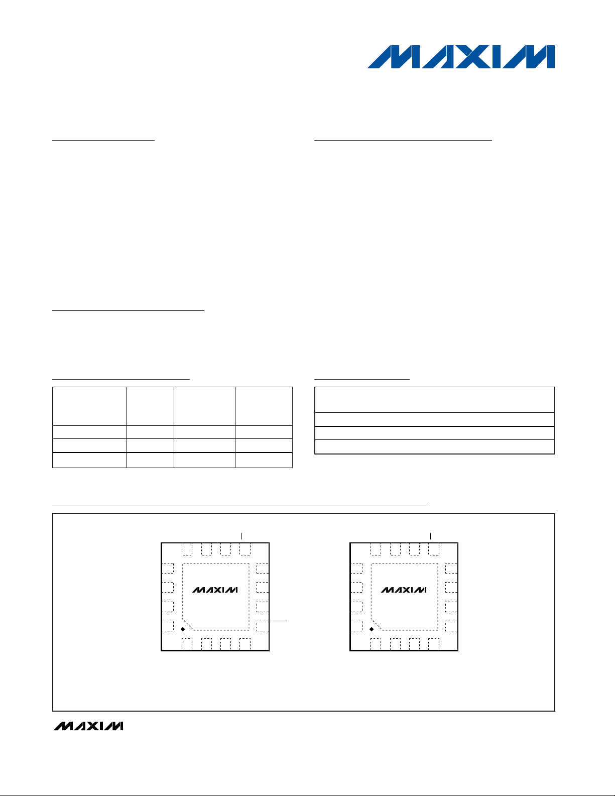
TOP VIEW
15
16
14
13
5
6
7
VP
VM
8
N.C.
D-
OE
V
TRM
13
V
BUS
4
12 10 9
V
L
BD
N.C.
SUS
GND
N.C.
*EP
MAX13483E
RCV D+
2
11
I.C.
TQFN
3mm x 3mm
15
16
14
13
5
6
7
VP
VM
8
SP (N.C.)
D-
OE
V
TRM
13
V
BUS
4
12 10 9
V
L
N.C. (BD)
N.C.
SUS
GND
ENUM
*EP
MAX13481E
MAX13482E
RCV D+
2
11
VPU (VPUR)
TQFN
3mm x 3mm
*EXPOSED PADDLE
*EXPOSED PADDLE
( ) MAX13482E ONLY
Pin Configurations
Ordering Information
Selector Guide
PART PIN-PACKAGE
TOP
PKG
CODE
MAX13481EETE
T1633-4
MAX13482EETE
T1633-4
MAX13483EETE
T1633-4
19-3801; Rev 2; 1/06
For pricing, delivery, and ordering information, please contact Maxim/Dallas Direct! at
1-888-629-4642, or visit Maxim’s website at www.maxim-ic.com.
Typical Operating Circuits appear at end of data sheet.
*EP = Exposed Paddle.
PART
ENUM
INPUT
MAX13481EETE ✓ ——
MAX13482EETE ✓✓ ✓
MAX13483EETE — — ✓
INTERNAL
1.5kΩ
RESISTOR
V
BUS
DETECTION
MARK
3mm X 3mm TQFN-EP* ADF
3mm X 3mm TQFN-EP* ADI
3mm X 3mm TQFN-EP* ADJ
Page 2
MAX13481E/MAX13482E/MAX13483E
±15kV ESD-Protected USB Transceivers with
External/Internal Pullup Resistors
2 _______________________________________________________________________________________
ABSOLUTE MAXIMUM RATINGS
ELECTRICAL CHARACTERISTICS
(V
CC
= +4V to +5.5V, VL= +1.6V to +3.6V, TA= T
MIN
to T
MAX
, unless otherwise noted. Typical values are at VCC= +5V, VL= +2.5V,
T
A
= +25°C.) (Note 1)
Stresses beyond those listed under “Absolute Maximum Ratings” may cause permanent damage to the device. These are stress ratings only, and functional
operation of the device at these or any other conditions beyond those indicated in the operational sections of the specifications is not implied. Exposure to
absolute maximum rating conditions for extended periods may affect device reliability.
(All voltages referenced to GND, unless otherwise noted.)
V
BUS
, V
L,
..................................................................-0.3V to +7V
V
TRM
, VPUR, VPU.....................................-0.3V to (V
BUS
+ 0.3V)
Input Voltage (D+, D-) ..............................................-0.3V to +7V
VM, VP, SUS, RCV,
ENUM, BD, OE, ............-0.3V to (VL+ 0.3V)
Short-Circuit Current to V
CC
or GND (D+, D-)… ........... ±150mA
Maximum Continuous Current (all other pins) ..................±15mA
Continuous Power Dissipation (T
A
= +70°C)
16-Pin, 3mm x 3mm TQFN (derate 15.6mW/°C above
+70°C).......................................................................1250mW
Operating Temperature Range ...........................-40°C to +85°C
Junction Temperature......................................................+150°C
Storage Temperature Range .............................-65°C to +150°C
Lead Temperature (soldering, 10s) .................................+300°C
PARAMETER
CONDITIONS
UNITS
SUPPLY INPUTS (V
BUS
, V
TRM
, VL)
V
BUS
Input Range V
BUS
4.0 5.5 V
VL Input Range V
L
1.6 3.6 V
Regulated Supply-Voltage Output
V
VTRM
3.0 3.3 3.6 V
Operating VCC Supply Current I
VCC
Full-speed transmitting/receiving at
10 mA
Operating VL Supply Current I
VL
Full-speed transmitting/receiving at
12Mbps, C
L
= 15pF receiver outputs,
V
L
= 2.5V (Note 2)
2.5 mA
Full-speed idle, VD+ > 2.7V, VD- < 0.3V
Full-Speed Idle and SE0 Supply
Current
)
SE0: VD+ < 0.3V, VD- < 0.3V
µA
Static VL Supply Current
)
Full-speed idle, SE0 or suspend mode 5 µA
Suspend Supply Current
)
35 µA
Disabled-Mode Supply Current
)
VL = GND or open 20 µA
Sharing-Mode VL Supply Current
)
V
BUS
= GND or open, OE = low,
VP = low or high, VM = low or high, SUS =
high, ENUM = high
5µA
Disable-Mode Load Current on
D+ and D-
)
VL = GND or open, VD_ = 0 or 5.5V 5 µA
Sharing-Mode Load Current on
D+ and D-
V
BUS
= GND or open, VD_ = 0 or 5.5V 20 µA
V
TH_H
Supply present 3.6
VL ≥ 1.7V 0.8
USB Power-Supply Detection
Threshold
V
TH_L
Supply lost
V
L
< 1.7V 0.7
V
USB Power-Supply Detection
Hysteresis
V
HYST
75 mV
VL Supply-Voltage Detection
Threshold
)
V
SYMBOL
MIN TYP MAX
12Mbps, CL = 50pF on D+ and D- (Note 2)
I
VCC(IDLE
I
VL(STATIC
I
VCC(SUSP
I
VCC(DIS
I
V L(S H ARIN G
I
D X (D IS ABLE
I
DX (SH ARING)
VM = VP = open, ENUM = SUS = OE = high
V
TH(VL
250 350
250 350
0.85
Page 3
MAX13481E/MAX13482E/MAX13483E
±15kV ESD-Protected USB Transceivers with
External/Internal Pullup Resistors
_______________________________________________________________________________________ 3
ELECTRICAL CHARACTERISTICS (continued)
(V
CC
= +4V to +5.5V, VL= +1.6V to +3.6V, TA= T
MIN
to T
MAX
, unless otherwise noted. Typical values are at VCC= +5V, VL= +2.5V,
T
A
= +25°C.) (Note 1)
PARAMETER
SYMBOL
CONDITIONS
MIN
TYP
MAX
UNITS
ANALOG VOLTAGE OUTPUTS (VPU, VPUR)
Off-State Leakage I
LZ
ENUM = V
L
-1 +1 µA
VPU Switch Resistance MAX13481E 10 Ω
VPUR Pullup Resistance MAX13482 (Note 3)
kΩ
DIGITAL INPUTS/OUTPUTS (VP,VM, RCV, OE, ENUM, SUS, BD)
Input-High Voltage V
IH
VP, VM, OE, ENUM, SUS
V
Input-Low Voltage V
IL
VP, VM, OE, ENUM, SUS
V
Output Voltage High V
OH
VP, VM, RCV, BD, I
SOURCE
= 2mA
V
Output Voltage Low V
OL
VP, VM, RCV, BD, I
SINK
= 2mA 0.4 V
Input Leakage Current I
LKG
-1 +1 µA
Input Capacitance Measured from input to GND 10 pF
ANALOG INPUT/OUTPUTS (D+, D-)
Differential Input Sensitivity V
DI
|(V
D+
- VD-)| 200 mV
Differential Common-Mode
Voltage Range
V
CM
Include V
DI
0.8 2.5 V
Single-Ended Input-Low Voltage
V
IL
0.8 V
Single-Ended Input-High Voltage
V
IH
2.0 V
Hysteresis V
HYS
250 mV
Output Voltage Low V
OL
RL = 1.5kΩ from D+ or D- to 3.6V 0.3 V
Output Voltage High V
OH
RL = 15kΩ to GND 2.8 3.6 V
Off-State Leakage Current Three-state driver -1 +1 µA
Transceiver Capacitance C
IND
D_ to GND 20 pF
Driver Output Impedance R
OUT
215Ω
ESD PROTECTION (D+, D-)
Human Body Model ±15 kV
IEC 61000-4-2 Contact Discharge
±8kV
TIMING CHARACTERISTICS
(V
CC
= +4V to +5.5V, VL= +1.6V to +3.6V, TA= T
MIN
to T
MAX
, unless otherwise noted. Typical values are at VCC= +5V, VL= +2.5V,
T
A
= +25°C.) (Note 1)
PARAMETER
SYMBOL
CONDITIONS
MIN
TYP
MAX
UNITS
DRIVER CHARACTERISTICS (CL = 50pF)
Rise Time D+/D- t
FR
10% to 90% of |VOH-VOL| (Figures 1, 9) 4 20 ns
Fall Time D+/D- t
FF
90% to 10% of |VOH-VOL| (Figures 1, 9) 4 20 ns
Rise- and Fall-Time Matching tFR/t
FF
Excluding the first transition from idle state,
(Figure 1) (Note 2)
90
%
1.425 1.575
0.7 x V
L
0.3 x V
VL - 0.4
L
110
Page 4
MAX13481E/MAX13482E/MAX13483E
±15kV ESD-Protected USB Transceivers with
External/Internal Pullup Resistors
4 _______________________________________________________________________________________
PARAMETER
SYMBOL
CONDITIONS
MIN
TYP
MAX
UNITS
Output Signal Crossover Voltage
V
CRS
(Figure 2) (Note 2) 1.3 2 V
Low-to-high transition (Figure 2) 18 ns
Driver Propagation Delay
High-to-low transition (Figure 2) 18 ns
Off-to-high transition (Figures 3, 10) 20 ns
Driver-Enabled Delay Time
Off-to-low transition (Figures 3, 10) 20 ns
High-to-off transition (Figures 3, 10) 20 ns
Driver Disabled Delay
Low-to-off transition (Figures 3, 10) 20 ns
RECEIVER (CL = 15pF)
Low-to-high transition (Figures 4, 9) 20
Differential Receiver
Propagation Delay
High-to-low transition (Figures 4, 9) 20
ns
Low-to-high transition (Figures 4, 9) 12
Single-Ended Receiver
Propagation Delay
High-to-low transition (Figures 4, 9) 12
ns
High-to-off transition (Figure 5) 15
Single-Ended Receiver Disable
Delay
Off-to-low transition (Figure 5) 15
ns
Off-to-high transition (Figure 5) 15
Single-Ended Receiver Enable
Delay
Off-to-low transition (Figure 5) 15
ns
TIMING CHARACTERISTICS (continued)
(V
CC
= +4V to +5.5V, VL= +1.6V to +3.6V, TA= T
MIN
to T
MAX
, unless otherwise noted. Typical values are at VCC= +5V, VL= +2.5V,
T
A
= +25°C.) (Note 1)
Note 1: Parameters are 100% production tested at +25°C, unless otherwise noted. Limits over temperature are guaranteed by
design.
Note 2: Guaranteed by design, not production tested.
Note 3: Including external 27Ω series resistor.
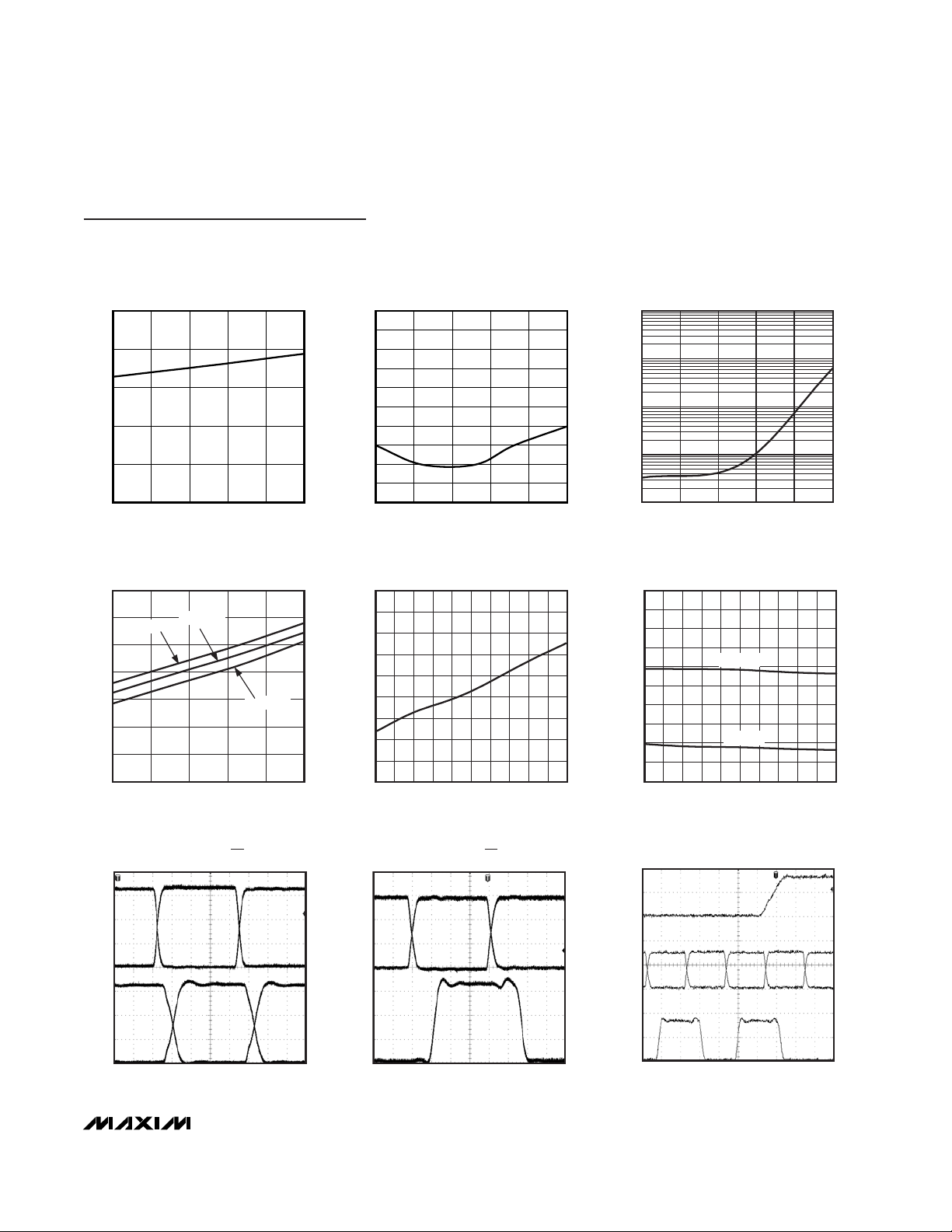
DIFFERENTIAL RECEIVER PROPAGATION
DELAY vs. TEMPERATURE
TEMPERATURE (°C)
PROPAGATION DELAY (ns)
MAX13481E toc02
-40 -15 10 35 60 85
6
7
8
9
10
11
12
13
14
15
16
SINGLE-ENDED RECEIVER PROPAGATION
DELAY vs. V
L
V
L
(V)
PROPAGATION DELAY (ns)
MAX13481 toc03
1.6 2.0 2.4 2.8 3.2 3.6
0
1
2
3
4
5
6
7
TA = +85°C
TA = +25°C
TA = -40°C
Typical Operating Characteristics
(V
BUS
= 5V, VL= +3.3V, TA= +25°C, unless otherwise noted.)
t
PLH_DRV
t
PHL_DRV
t
PZH_DRV
t
PZL_DRV
t
PHZ_DRV
t
PLZ_DRV
t
PLH_RCV
t
PHL_RCV
t
PLH_SE
t
PHL_SE
t
PHZ_SE
t
PLZ_SE
t
PZH_SE
t
PZL_SE
DIFFERENTIAL RECEIVER
14.0
PROPAGATION DELAY vs. V
13.5
13.0
12.5
12.0
11.5
11.0
PROPAGATION DELAY (ns)
10.5
10.0
1.6 2.0 2.4 2.8 3.2 3.6
TA = +85°C
TA = +25°C
TA = -40°C
V
(V)
L
L
MAX13481E toc01
Page 5
MAX13481E/MAX13482E/MAX13483E
±15kV ESD-Protected USB Transceivers with
External/Internal Pullup Resistors
_______________________________________________________________________________________ 5
SINGLE-ENDED RECEIVER PROPAGATION
DELAY vs. TEMPERATURE
TEMPERATURE (°C)
PROPAGATION DELAY (ns)
MAX13481E toc04
-40 -15 10 35 60 85
0
1
2
3
4
5
TRANSMITTER SKEW
vs. TEMPERATURE
TEMPERATURE (°C)
TRANSMITTER SKEW (ns)
MAX13481E toc05
-40 -15 10 35 60 85
0
0.2
0.4
0.6
0.8
1.0
1.2
1.4
1.6
1.8
2.0
0
4
2
8
6
10
12
16
14
18
0102030405060708090100
V
BUS
SUPPLY CURRENT
vs. D+/D- CAPACITANCE
MAX13481E toc08
CAPACITANCE (pF)
V
BUS
SUPPLY CURRENT (mA)
1.00
1.10
1.05
1.20
1.15
1.25
1.30
1.40
1.45
1.35
1.50
0102030405060708090100
VL SUPPLY CURRENT
vs. D+/D- CAPACITANCE
MAX13481E toc09
CAPACITANCE (pF)
V
BUS
SUPPLY CURRENT (mA)
VL = 2.5V
VL = 1.8V
Typical Operating Characteristics (continued)
(V
BUS
= 5V, VL= +3.3V, TA= +25°C, unless otherwise noted.)
v
v
V
SUSPEND CURRENT
BUS
vs. V
20
19
TA = +85°C
18
BUS
TA = +25°C
MAX13481E toc07
VL SUSPEND CURRENT
100
10
1
SUSPEND CURRENT (μA)
L
V
0.1
0.01
-40 -15 35 8560
vs. TEMPERATURE
10
TEMPERATURE (°C)
MAX13481E toc06
17
16
SUPPLY CURRENT (μA)
15
BUS
V
14
13
4.0 4.3 4.6 4.9 5.2 5.5
TRANSMIT MODE (OE = LOW)
TA = -40°C
V
(V)
BUS
SUSPEND MODE
20ns/div
MAX13481E toc12
10ns/div
MAX13481E toc10
VP
1V/div
VM
D+
1V/div
D-
RECEIVE MODE (OE = HIGH)
10ns/div
MAX13481E toc11
D+
1V/di
D-
RCV
1V/di
SUS
2V/div
D+
2V/div
D-
RCV
2V/div
Page 6
MAX13481E/MAX13482E/MAX13483E
±15kV ESD-Protected USB Transceivers with
External/Internal Pullup Resistors
6 _______________________________________________________________________________________
EYE DIAGRAM
MAX13481E toc16
4
-1
2
1
0
3
0 1020304050607080
TIME (ns)
D+ AND D- (V)
Pin Description
Typical Operating Characteristics (continued)
(V
BUS
= 5V, VL= +3.3V, TA= +25°C, unless otherwise noted.)
PIN
MAX13481E
MAX13482E
MAX13483E
NAME
FUNCTION
8, 16
1, 8
8
No Connection. Not internally connected.
1——SP
Connect to V
L
for Pin Compatibility to the MIC2551A or Leave Floating. Not internally
connected.
222
Differential Receiver Output. RCV responds to the differential input on D+ and D-. RCV
asserts low when SUS = V
L.
333VP
Receiver Output/Driver Input. VP functions as a receiver output when OE = V
L
. VP
duplicates D+ when receiving. VP functions as a driver input when OE = GND.
TRANSMISSION IN
SUSPEND MODE
MAX13481E toc13
D+
1V/div
D-
VP
BUS DETECT RESPONSE
MAX13481E toc14
V
BUS
2V/div
1V/div
20ns/div
OE, VP, VM TIMING
20ns/div
MAX13481E toc15
VM
OE
2V/div
VP
2V/div
VM
2V/div
1μs/div
BD
1V/div
1, 5,
N.C.
RCV
Page 7
MAX13481E/MAX13482E/MAX13483E
±15kV ESD-Protected USB Transceivers with
External/Internal Pullup Resistors
_______________________________________________________________________________________ 7
Pin Description (continued)
PIN
NAME
FUNCTION
444VM
Receiver Output/Driver Input. VM functions as a receiver output when OE = V
L
. VM
duplicates D- when receiving. VM functions as a driver input when OE = GND.
55—
Active-Low Enumerator-Function-Selection Input. ENUM controls the pullup resistor or
switch connection. See the
ENUM
section.
666
Ground
777
Suspend Input. Drive SUS low for normal operation. Drive SUS high for low-power state.
RCV asserts low and D+/ D- are high impedance in suspend mode. VP and VM remain
active in suspend mode.
999OE
Output Enable. Drive OE to GND to enable the D+/D- transmitter outputs. Drive OE to V
L
to
disable the transmitter outputs. OE also controls the I/O directions of VP and VM (see
Tables 3 and 4).
10 10 10 D-
USB Input/Output. For OE = GND, D- functions as a USB output with VM providing the input
signal. For OE = VL, D- functions as a USB input with VM functioning as a single-ended
receiver output.
11 11 11 D+
USB Input/Output. For OE = GND, D+ functions as a USB output with VP providing the
input signal. For OE = V
L
, D+ functions as a USB input with VP functioning as a single-
ended receiver output.
12 12 12
Regulated Output Voltage. V
TRM
provides a 3.3V output derived from V
BUS
. Bypass V
TRM
to GND with a 1µF (min) low-ESR capacitor such as ceramic or plastic film types. V
TRM
provides power to internal circuitry, the internal D+ pullup resistor, VPU and VPUR. Do not
use V
TRM
to power external circuitry.
13 — —
Pullup Voltage. For ENUM = GND, VPU is pulled to an internal 3.3V voltage. Connect a
1.5kΩ resistor between D+ and VPU for full-speed operation. For ENUM = V
L
, VPU is high
impedance.
— — 13 I.C. Internally Connected. Leave open. Do not connect to external circuitry.
—13—
Internal Pullup Resistor. VPUR is pulled to an internal 3.3V voltage through a 1.5kΩ resistor
(ENUM = GND). Connect VPUR to D+ for full-speed operation. For ENUM = V
L
, VPU is
high impedance.
14 14 14
USB-Side Power-Supply Input. Connect a +4V to +5.5V power supply to V
BUS
. V
BUS
supplies power to the internal regulator. Bypass V
BUS
to GND with a 1µF ceramic
capacitor. Connect V
BUS
and V
TRM
together when powering the MAX13481E/MAX13482E/
MAX13483E with an external power supply.
15 15 15 V
L
Digital Input/Output Connection Logic Supply. Connect a +1.6V to +3.6V supply to VL.
Bypass V
L
to GND with a 0.1µF (min) low-ESR ceramic capacitor.
— 16 16 BD USB Detector Output (Push/Pull). A high at BD signals to the ASIC that V
BUS
is present.
EP EP EP EP Exposed Paddle. Connect EP to GND.
ENUM
GND
SUS
V
TRM
VPU
VPUR
V
BUS
Page 8

MAX13481E/MAX13482E/MAX13483E
±15kV ESD-Protected USB Transceivers with
External/Internal Pullup Resistors
8 _______________________________________________________________________________________
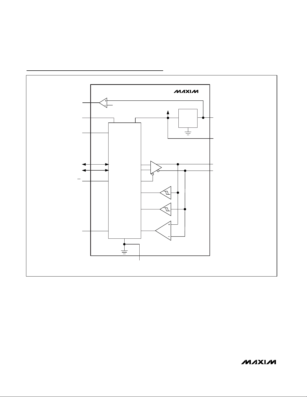
Detailed Description
The MAX13481E/MAX13482E/MAX13483E ±15kV ESDprotected USB-compliant transceivers convert singleended or differential logic-level signals to USB signals,
and USB signals to single-ended or differential logic
signals. These devices fully comply to USB 2.0 when
operating at full-speed (12Mbps), and operate with V
L
as low as 1.6V, ensuring compatibility with low-voltage
ASICs. Integrated ±15kV ESD-circuitry protection protects D+ and D- bus connections.
The MAX13481E/MAX13483E require an external 1.5kΩ
pullup resistor to V
TRM
for full-speed operation. The
MAX13481E requires an external 1.5kΩ pullup resistor
and feature an active-low enumeration function that
connects a +3.3V voltage at VPU. The MAX13482E features an active-low enumeration function that connects
a 1.5kΩ pullup resistor at VPUR for full-speed operation. The MAX13482E/MAX13483E also provide a bus
detect (BD) output that asserts high when V
BUS
> 3.6V.
Applications Information
Power-Supply Configurations
Normal Operating Mode
Connect VLand V
BUS
to system power supplies (Table 1).
Connect V
L
to a +1.6V to +3.6V supply. Connect V
BUS
to a +4.0V to +5.5V supply or to the V
BUS
connector.
Alternatively, these parts can derive power from a single Li+ cell. Connect the battery to V
BUS
. V
TRM
remains
above +3.0V for V
BUS
as low as +3.1V. Additionally, the
devices can be powered by an external +3.3V ±10%
voltage regulator. Connect V
BUS
and V
TRM
to an exter-
nal +3.3V voltage regulator. V
BUS
no longer consumes
current to power the internal linear regulator in this configuration. The bus detect function (BD) on the
MAX13482E and MAX13483E does not function when
the device is powered this way.
Disable Mode
Connect V
BUS
to a system power supply and leave V
L
unconnected or connect to GND. D+ and D- enter a tristate mode and V
BUS
(or V
BUS
and V
TRM
) consumes
less than 20µA of supply current. D+ and D- withstand
external signals up to +5.5V in disable mode (Table 2).
V
BUS
(V) V
TRM
(V) VL (V) CONFIGURATION NOTES
+4.0 to +5.5 +3.0 to +3.6 output +1.6 to +3.6 Normal mode —
+4.0 to +5.5 +3.0 to +3.6 output GND or floating Disable mode Table 2
GND or floating High Z +1.6 to +3.6 Sharing mode Table 2
+3.1 to +4.5 +3.0 to +3.6 output +1.6 to +3.6 Battery supply
+3.0 to +3.6 +3.0 to +3.6 input +1.6 to +3.6
—
Table 1. Power-Supply Configuration
INPUTS/OUTPUTS DISABLE MODE SHARING MODE
V
BUS
/ V
TRM
4V to 5.5V Floating or connected to GND
V
L
Floating or connected to GND 1.6V to 3.6V input
D+ and D- High impedance High impedance
For OE = low, high impedance
VP and VM Invalid*
For OE = high, output logic high
RCV Invalid* Undefined
BD
(MAX13482E/MAX13483E)
Invalid* Low
Table 2. Disable-Mode and Sharing-Mode Connection
*High impedance or logic low
Voltage regulator supply
Page 9

Sharing Mode
Connect VLto a system power supply and leave V
BUS
(or V
BUS
and V
TRM
) unconnected or connect to GND.
D+ and D- enter a tri-state mode, allowing other circuitry
to share the USB D+ and D- lines. VLconsumes less
than 20µA of supply current. D+ and D- withstand external signals up to +5.5V in sharing mode (Table 2).
Device Control
OE
OE controls the direction of communication. Drive OE
low to transfer data from the logic side to the USB side.
For OE = low, VP and VM serve as differential driver
inputs to the USB transmitter. Drive OE high to transfer
data from the USB side to the logic side. For OE = high,
VP and VM serve as single-ended receiver outputs
from the USB inputs (D+ and D-). RCV serves as a differential receiver output, regardless of the state of OE.
ENUM
(MAX13481E/MAX13482E)
The MAX13481E/MAX13482E feature an active-low enumerate function that allows software control of the 1.5kΩ
pullup resistor and switch to D+ for full-speed operation.
For the MAX13481E, connect a 1.5kΩ pullup resistor
between D+ and VPU. The MAX13481E provides an
internal switch that pulls VPU to a +3.3V voltage. Drive
ENUM high to disconnect VPU from voltage. Drive
ENUM low to connect VPU and the external pullup resis-
tor to the +3.3V voltage.
The MAX13482E has an internal 1.5kΩ resistor that
connects at VPUR. Connect VPUR directly to D+. Drive
ENUM high to disconnect the internal pullup resistor at
VPUR. Drive ENUM low to connect the internal pullup
resistor to VPUR.
SUS
The SUS state determines whether the MAX13481E/
MAX13482E/MAX13483E operate in normal mode or in
suspend mode. Connect SUS to GND to enable normal
operation. Drive SUS high to enable suspend mode.
RCV asserts low and VP and VM remain active in suspend mode (Tables 3 and 4). In suspend mode, supply
current is reduced.
MAX13481E/MAX13482E/MAX13483E
±15kV ESD-Protected USB Transceivers with
External/Internal Pullup Resistors
_______________________________________________________________________________________ 9
INPUTS OUTPUTS
VP VM D+ D-
0000
0101
1010
1111
Table 3. Transmit Truth Table
(OE = 0)
INPUTS OUTPUTS
D+ D- VP VM RCV
0 0 0 0 RCV*
01010
10101
1111X
Table 4a. Receive Truth Table
(OE = 1)
INPUTS OUTPUTS
D+ D- VP VM RCV
00000
01010
10100
11110
Table 4b. Receive Truth Table
(OE = 1, SUS = 1)
* = Last state
X = Undefined
Page 10

MAX13481E/MAX13482E/MAX13483E
±15kV ESD-Protected USB Transceivers with
External/Internal Pullup Resistors
10 ______________________________________________________________________________________
V
TRM
An internal linear regulator generates the V
TRM
voltage
(+3.3V, typ). V
TRM
derives power from V
BUS
(see the
Power-Supply Configurations section). V
TRM
powers
the internal portions of the USB circuitry and provides
the pullup voltage for the MAX13481E/MAX13482E.
Bypass V
TRM
to GND with a 1µF ceramic capacitor as
close to the device as possible. Do not use V
TRM
to pro-
vide power to any other external circuitry.
D+ and D-
D+ and D- serve as bidirectional bus connections and
are ESD-protected to ±15kV (Human Body Model). For
OE = low, D+ and D- serve as transmitter outputs. For
OE = high, D+ and D- serve as receiver inputs.
BD (MAX13482E/MAX13483E)
The push-pull bus detect (BD) output monitors V
BUS
and asserts high if V
BUS
is greater than V
TH_H
. BD
asserts low if V
BUS
is less than V
TH_L
, and the
MAX13482E/MAX13483E enter sharing mode (Table 2).
V
BUS
For most applications, V
BUS
connects to the V
BUS
terminal on the USB connector (see the Power-Supply
Configurations section). V
BUS
can also connect to an
external supply. Drive V
BUS
low to enable sharing
mode. Bypass V
BUS
to GND with a 1µF ceramic capac-
itor as close to the device as possible.
External Components
External Capacitors
The MAX13481E/MAX13482E/MAX13483E require
three external capacitors for proper operation. Bypass
V
L
to GND with a 0.1µF ceramic capacitor. Bypass
V
BUS
to GND with a 1µF ceramic capacitor. Bypass
V
TRM
to GND with a 1µF (min) ceramic capacitor.
Install all capacitors as close to the device as possible.
External Resistor
Proper USB operation requires two external resistors,
each 27Ω ±1%. Install one resistor in series between D+
of the MAX13481E/MAX13482E/MAX13483E and D+ on
the USB connector. Install the other resistor in series
between D- of the MAX13481E/MAX13482E/MAX13483E
and D- on the USB connector (see the Typical Operating
Circuits). The MAX13483E requires an external 1.5kΩ
pullup resistor between V
TRM
and D+ for full-speed
operation. The MAX13481E requires an external 1.5kΩ
pullup resistor between VPU and D+ for full-speed operation. The MAX13482E does not require an external
pullup resistor but VPUR must be connected to D+ for
full-speed operation.
Data Transfer
Transmitting Data to the USB
To transmit data to the USB, drive OE low. The
MAX13481E/MAX13482E/MAX13483E transmit data to
the USB differentially on D+ and D-. VP and VM serve
as input signals to the differential driver and are also
used to assert a single-ended zero (SE0) driver (see
Table 3).
Receiving Data from the USB
To receive data from the USB, drive OE high and SUS
low. Differential data received by D+ and D- appears at
RCV. Single-ended receivers on D+ and D- drive VP
and VM, respectively.
RCV
RCV monitors D+ and D- when receiving data. RCV is a
logic 1 for D+ high and D- low. RCV is a logic 0 for D+
low and D- high. RCV retains its last valid state when
D+ and D- are both low (single-ended zero, or SE0).
ESD Protection
D+ and D- possess extra protection against static electricity to protect the devices up to ±15kV. The ESD
structures withstand high ESD in all operating modes:
normal operation, suspend mode, and powered down.
D+ and D- provide protection to the following limits:
•±15kV using the Human Body Model
•±8kV using the Contact Discharge method specified
in IEC 61000-4-2
• To protect V
BUS
from ±15kV ESD, a 1µF or greater
capacitor must be connected from V
BUS
to GND.
ESD Test Conditions
ESD performance depends on a variety of conditions.
Contact Maxim for a reliability report that documents
test setup, test methodology, and test results.
Human Body Model
Figure 6 shows the Human Body Model and Figure 7
shows the current waveform generated when discharged into a low impedance. This model consists of
a 100pF capacitor charged to the ESD voltage of interest, which then discharges into the test device through
a 1.5kΩ resistor.
IEC 61000-4-2
The IEC 61000-4-2 standard covers ESD testing and
performance of finished equipment. It does not specifically refer to integrated circuits. The major difference
between tests done using the Human Body Model and
IEC 61000-4-2 is a higher peak current in IEC 61000-42, due to lower series resistance. Hence, the ESD with-
Page 11

stand voltage measured to IEC 61000-4-2 generally is
lower than that measured using the Human Body
Model. Figure 8 shows the IEC 61000-4-2 model. The
Contact Discharge method connects the probe to the
device before the probe is charged.
Machine Model
The Machine Model for ESD tests all connections using
a 200pF storage capacitor and zero discharge resis-
tance. Its objective is to emulate the stress caused by
contact that occurs with handling and assembly during
manufacturing. All pins require this protection during
manufacturing, not just inputs and outputs. After PC
board assembly, the Machine Model is less relevant to
I/O ports.
MAX13481E/MAX13482E/MAX13483E
±15kV ESD-Protected USB Transceivers with
External/Internal Pullup Resistors
______________________________________________________________________________________ 11
V
OHD
V
OLD
90%
10%
90%
10%
t
FR
, t
LR
tFF, t
LF
Figure 1. Rise and Fall Times
VM
VP
D-
D+
t
PLH_DRV
t
PHL_DRV
V
CRS_F
, V
CRS_L
VP AND VM RISE/FALL TIMES < 4ns
Figure 2. Timing of VP and VM to D+ and D-
OE
D+/D-
t
PLZ_DRV
t
PZL_DRV
t
PHZ_DRV
t
PZH_DRV
VP/VM CONNECTED TO GND,
D+/D- CONNECTED
TO PULLUP
VP/VM
CONNECTED TO VL,
D+/D- CONNECTED
TO PULLDOWN
OE
D+/D-
Figure 3. Driver’s Enable and Disable Timing
Timing Diagrams
Page 12

MAX13481E/MAX13482E/MAX13483E
±15kV ESD-Protected USB Transceivers with
External/Internal Pullup Resistors
12 ______________________________________________________________________________________
Timing Diagrams (continued)
+3V
0V
RCV, VM, AND VP
V
L
D+/D-
t
PLH_RCV
,
t
PLH_SE
t
PHL_RCV
,
t
PHL_SE
INPUT RISE/FALL TIME < 4ns
Figure 4. D+/D- Timing to VP, VM, and RCV
CHARGE-CURRENT-
LIMIT RESISTOR
DISCHARGE
RESISTANCE
STORAGE
CAPACITOR
C
s
100pF
R
C
1MΩ
R
D
1.5kΩ
HIGH-
VOLTAGE
DC
SOURCE
DEVICE
UNDER
TEST
Figure 6. Human Body ESD Test Model
IP 100%
90%
36.8%
t
RL
TIME
t
DL
CURRENT WAVEFORM
PEAK-TO-PEAK RINGING
(NOT DRAWN TO SCALE)
I
r
10%
0
0
AMPERES
Figure 7. Human Body Model Current Waveform
OE
VP/VM
VP/VM
t
PLZ_SE
t
PZL_SE
t
PHZ_SE
t
PZH_SE
D+/D- CONNECTED TO GND,
VP/VM CONNECTED
TO PULLUP
D+/D-
CONNECTED TO +3V,
VP/VM CONNECTED
TO PULLDOWN
OE
Figure 5. Receiver’s Enable and Disable Timing
CHARGE-CURRENT-
LIMIT RESISTOR
DISCHARGE
RESISTANCE
STORAGE
CAPACITOR
C
s
150pF
R
C
50Ω to 100Ω
R
D
330Ω
HIGH-
VOLTAGE
DC
SOURCE
DEVICE
UNDER
TEST
Figure 8. IEC 61000-4-2 ESD Test Model
Page 13

MAX13481E/MAX13482E/MAX13483E
±15kV ESD-Protected USB Transceivers with
External/Internal Pullup Resistors
______________________________________________________________________________________ 13
MAX13481E
MAX13482E
MAX13483E
RCV, VM,
AND VP
TEST
POINT
(a) LOAD FOR RCV, VM, AND VP
MAX13481E
MAX13482E
MAX13483E
D+ AND D-
27Ω
15kΩ
C
L
C
L
TEST
POINT
(b) LOAD FOR D+/D-
Figure 9. Transmitter and Receiver Propagation Delay
Test Circuits
Figure 10. Driver’s Enable and Disable Timing
TEST
POINT
27Ω
DUT
D+/D-
C
L
220Ω
+
-
Page 14

MAX13481E/MAX13482E/MAX13483E
±15kV ESD-Protected USB Transceivers with
External/Internal Pullup Resistors
14 ______________________________________________________________________________________
LEVEL
TRANSLATOR
AND LOGIC
D+
D-
OE
V
L
LDO
REGULATOR
TO INTERNAL
CIRCUITRY
V
TRM
VPU
V
BUS
MAX13481E
ENUM
RCV
SUS
VM
VP
GND
Functional Diagrams
Page 15

MAX13481E/MAX13482E/MAX13483E
±15kV ESD-Protected USB Transceivers with
External/Internal Pullup Resistors
______________________________________________________________________________________ 15
Functional Diagrams (continued)
LEVEL
TRANSLATOR
AND LOGIC
D+
D-
BD
V
TH_VBUS
OE
V
L
LDO
REGULATOR
TO INTERNAL
CIRCUITRY
V
TRM
VPUR
V
BUS
MAX13482E
ENUM
RCV
SUS
VM
VP
GND
Page 16
MAX13481E/MAX13482E/MAX13483E
±15kV ESD-Protected USB Transceivers with
External/Internal Pullup Resistors
16 ______________________________________________________________________________________
Functional Diagrams (continued)
LEVEL
TRANSLATOR
AND LOGIC
D+
D-
BD
V
TH
OE
V
L
LDO
REGULATOR
TO INTERNAL
CIRCUITRY
V
TRM
V
BUS
MAX13483E
RCV
GND
SUS
VM
VP
Page 17
MAX13481E/MAX13482E/MAX13483E
±15kV ESD-Protected USB Transceivers with
External/Internal Pullup Resistors
______________________________________________________________________________________ 17
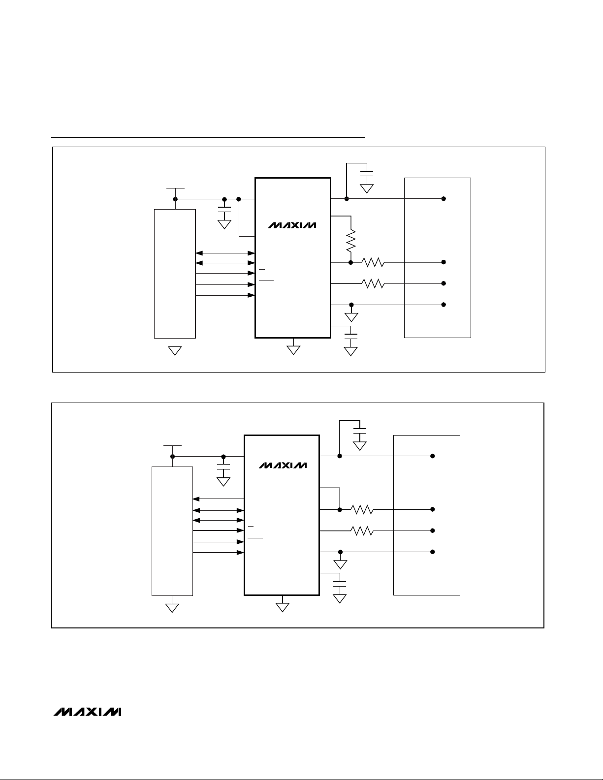
Typical Operating Circuits
MAX13482E
SYSTEM
SUPPLY
VOLTAGE
V
BUS
V
L
SYSTEM
INTERFACE
VM
VP
GND
D-
D+
GND
D-
D+
V
PUR
V
TRM
SUS
BD
ENUM
OE
PC
27Ω ±1%
27Ω ±1%
USB
POWER
0.1μF
1μF
1μF
SYSTEM
SUPPLY
VOLTAGE
SYSTEM
INTERFACE
0.1μF
V
L
SP
VM
VP
OE
ENUM
SUS
MAX13481E
V
VPU
GND
V
BUS
TRM
1μF
PC
USB
POWER
1.5kΩ
D+
D-
27Ω ±1%
D+
27Ω ±1%
D-
GND
1μF
Page 18

MAX13481E/MAX13482E/MAX13483E
±15kV ESD-Protected USB Transceivers with
External/Internal Pullup Resistors
18 ______________________________________________________________________________________
Chip Information
PROCESS: BiCMOS
Typical Operating Circuits (continued)
MAX13483E
SYSTEM
SUPPLY
VOLTAGE
V
BUS
V
TRM
V
L
SYSTEM
INTERFACE
VM
VP
GND
D-
D+
GND
D-
D+
SUS
BD
ENUM
OE
PC
27Ω ±1%
27Ω ±1%
USB
POWER
0.1μF
1μF
1.5kΩ
1μF
Page 19

MAX13481E/MAX13482E/MAX13483E
±15kV ESD-Protected USB Transceivers with
External/Internal Pullup Resistors
Maxim cannot assume responsibility for use of any circuitry other than circuitry entirely embodied in a Maxim product. No circuit patent licenses are
implied. Maxim reserves the right to change the circuitry and specifications without notice at any time.
Maxim Integrated Products, 120 San Gabriel Drive, Sunnyvale, CA 94086 408-737-7600 ____________________ 19
© 2006 Maxim Integrated Products Printed USA is a registered trademark of Maxim Integrated Products, Inc.
Package Information
(The package drawing(s) in this data sheet may not reflect the most current specifications. For the latest package outline information
go to www.maxim-ic.com/packages
.)
12x16L QFN THIN.EPS
0.10 C 0.08 C
0.10 M C A B
D
D/2
E/2
E
A1
A2
A
E2
E2/2
L
k
e
(ND - 1) X e
(NE - 1) X e
D2
D2/2
b
L
e
L
C
L
e
C
L
L
C
L
C
PACKAGE OUTLINE
21-0136
2
1
F
12, 16L THIN QFN, 3x3x0.8mm
MARKING
AAAA
1. DIMENSIONING & TOLERANCING CONFORM TO ASME Y14.5M-1994.
EXPOSED PAD VARIATIONS
1.10T1633-1 0.95
CODES
PKG.
T1233-1
MIN.
0.95
NOM.
1.10
D2
1.251.100.951.25
NOM.
1.10
MAX.
1.25
MIN.
0.95
MAX.
1.25
E2
12
N
k
A2
0.25
NE
A1ND0
0.20 REF
-
-
3
0.0230.05
L
e
E
0.45
2.90
b
D
A
0.20
2.90
0.70
0.50 BSC.
0.55
3.00
0.65
3.10
0.25
3.00
0.75
0.30
3.10
0.80
16
0.20 REF
0.25
-
040.02
4
-
0.05
0.50 BSC.
0.30
2.90
0.40
3.00
0.20
2.90
0.70
0.25
3.00
0.75
3.10
0.50
0.80
3.10
0.30
PKG
REF. MIN.
12L 3x3
NOM. MAX. NOM.
16L 3x3
MIN. MAX.
0.35 x 45°
PIN ID
JEDEC
WEED-1
0.35 x 45° WEED-2
2. ALL DIMENSIONS ARE IN MILLIMETERS. ANGLES ARE IN DEGREES.
3. N IS THE TOTAL NUMBER OF TERMINALS.
4. THE TERMINAL #1 IDENTIFIER AND TERMINAL NUMBERING CONVENTION SHALL CONFORM TO
JESD 95-1 SPP-012. DETAILS OF TERMINAL #1 IDENTIFIER ARE OPTIONAL, BUT MUST BE LOCATED
WITHIN THE ZONE INDICATED. THE TERMINAL #1 IDENTIFIER MAY BE EITHER A MOLD OR
MARKED FEATURE.
5. DIMENSION b APPLIES TO METALLIZED TERMINAL AND IS MEASURED BETWEEN 0.20 mm AND 0.25 mm
FROM TERMINAL TIP.
6. ND AND NE REFER TO THE NUMBER OF TERMINALS ON EACH D AND E SIDE RESPECTIVELY.
7. DEPOPULATION IS POSSIBLE IN A SYMMETRICAL FASHION.
8. COPLANARITY APPLIES TO THE EXPOSED HEAT SINK SLUG AS WELL AS THE TERMINALS.
9. DRAWING CONFORMS TO JEDEC MO220 REVISION C.
NOTES:
T1233-3 1.10 1.25 0.95 1.10
0.35 x 45°1.25 WEED-10.95
T1633F-3 0.65
T1633-4
0.95
0.80
0.95
0.65
0.80
1.10
1.25
0.95
1.10
0.225 x 45°
0.95
WEED-2
0.35 x 45°
1.25
WEED-2
T1633-2 0.95
1.10
1.25
0.95
1.10
0.35 x 45°
1.25
WEED-2
NO
DOWN
BONDS
ALLOWED
YES
NO
YES
N/A
NO
PACKAGE OUTLINE
21-0136
2
2
F
12, 16L THIN QFN, 3x3x0.8
YESWEED-11.251.100.95 0.35 x 45°1.251.100.95T1233-4
T1633FH-3 0.65
0.80
0.95
0.225 x 45°0.65
0.80 0.95
WEED-2
N/A
10. MARKING IS FOR PACKAGE ORIENTATION REFERENCE ONLY
11. NUMBER OF LEADS SHOWN ARE FOR REFERENCE ONLY
 Loading...