

Page 1
General Description
The MAX1338 14-bit, analog-to-digital converter (ADC)
offers four simultaneously sampled, fully differential input
channels, with independent track-and-hold (T/H) circuitry
for each channel. The input channels are individually
software programmable for input ranges of ±10V, ±5V,
±2.5V, and ±1.25V. The input channels feature fault tolerance to ±17V. The internal T/H circuits have a 16ns
aperture delay and 100ps aperture-delay matching.
A 14-bit parallel bus provides the conversion result with
a maximum per-channel output rate of 150ksps
(600ksps for all four channels). The MAX1338 has an
on-board oscillator and 2.5V internal reference. An
external clock and/or reference can also be used.
The MAX1338 operates from a +5V supply for analog
inputs and digital core. The device operates from a +2.7V
to +5.25V supply for the digital I/O lines. The MAX1338
features two power-saving modes: standby mode and
shutdown mode. Standby mode allows rapid wake-up
and reduces quiescent current to 4mA (typ), and shutdown mode reduces sleep current to less than 10µA (typ).
The MAX1338 is available in an 8mm x 8mm x 0.8mm,
56-pin, thin QFN package. The device operates over
the extended -40°C to +85°C temperature range.
Applications
Multiple-Channel Data Recorders
Vibration Analysis
Motor Control: 3-Phase Voltage, Current, and
Power Measurement
Optical Communication Equipment
Features
♦ 150ksps Sample Rate per Channel
♦ All Four Input Channels Simultaneously Sampled
16ns Aperture Delay
100ps Aperture-Delay Matching
♦ Channel-Independent Software-Selectable Input
Range: ±10V, ±5V, ±2.5V, ±1.25V
♦ ±17V Fault-Tolerant Inputs
♦ Dynamic Performance at 10kHz Input
SNR: 77dB
SINAD: 76dB
SFDR: 98dBc
THD: -83dBc
♦ DC Performance
INL: ±2 LSB
DNL: ±1 LSB
Offset Error: ±4 LSB
Gain Error: ±0.1% FSR
♦ 14-Bit Parallel Interface
♦ Internal Clock and Reference Voltage
♦ +5V Analog and Digital Supplies
♦ +2.7V to +5.25V Digital I/O Supply
♦ 56-Pin Thin QFN Package (8mm x 8mm x 0.8mm)
MAX1338
14-Bit, 4-Channel, Software-Programmable,
Multiranging, Simultaneous-Sampling ADC
________________________________________________________________ Maxim Integrated Products 1
Ordering Information
19-3151; Rev 0; 4/04
For pricing, delivery, and ordering information, please contact Maxim/Dallas Direct! at
1-888-629-4642, or visit Maxim’s website at www.maxim-ic.com.
PART TEMP RANGE PIN-PACKAGE
MAX1338ETN -40°C to +85°C 56 Thin QFN-EP*
*EP = Exposed pad.
Pin Configuration appears at end of data sheet.
Page 2
MAX1338
14-Bit, 4-Channel, Software-Programmable,
Multiranging, Simultaneous-Sampling ADC
2 _______________________________________________________________________________________
ABSOLUTE MAXIMUM RATINGS
Stresses beyond those listed under “Absolute Maximum Ratings” may cause permanent damage to the device. These are stress ratings only, and functional
operation of the device at these or any other conditions beyond those indicated in the operational sections of the specifications is not implied. Exposure to
absolute maximum rating conditions for extended periods may affect device reliability.
AVDDto AGND .........................................................-0.3V to +6V
DV
DD
to DGND.........................................................-0.3V to +6V
DRV
DD
to DRGND....................................................-0.3V to +6V
AV
DD
to DVDD.......................................................-0.3V to +0.3V
DGND to DRGND..................................................-0.3V to +0.3V
AGND to DGND.....................................................-0.3V to +0.3V
AGND to DRGND ..................................................-0.3V to +0.3V
AIN0+, AIN0-, AIN1+, AIN1-, AIN2+, AIN2-, AIN3+,
AIN3- to AGND.....................................................-17V to +17V
D0–D13 to DRGND................................-0.3V to (DRV
DD
+ 0.3V)
REFADC, REFP1, REFP2, REFN1, REFN2, COM1, COM2 to
AGND....................................................-0.3V to (AV
DD
+ 0.3V)
INTCLK/
EXTCLK to AGND.......................-0.3V to (AVDD+ 0.3V)
CS, RD, WR, CONVST, to DRGND........-0.3V to (DRV
DD
+ 0.3V)
SHDN, STANDBY, CLK, EOC,
EOLC to DRGND................................-0.3V to (DRV
DD
+ 0.3V)
Maximum Current into Any Pin .........................................±50mA
Continuous Power Dissipation (T
A
= +70°C)
56-Pin Thin QFN (derate 31.3mW /°C above +70°C)....2500mW
Operating Temperature Range ...........................-40°C to +85°C
Storage Temperature Range .............................-65°C to +150°C
Maximum Junction Temperature .....................................+150°C
Lead Temperature (soldering, 10s) .................................+300°C
Junction to Ambient Thermal Resistance θ
JA
..................32°C/W
Junction to Case Thermal Resistance θ
JC
.........................2°C/W
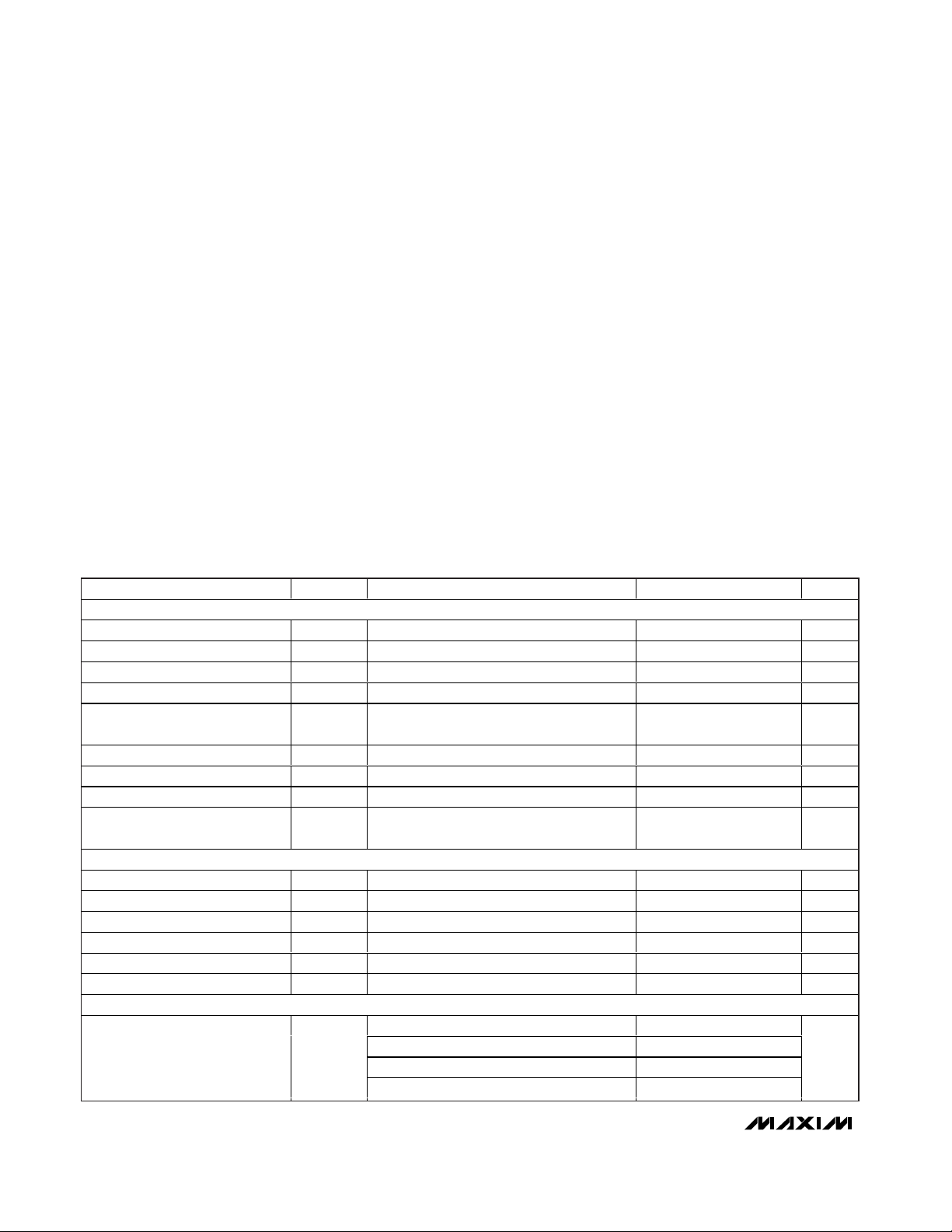
ELECTRICAL CHARACTERISTICS
(AVDD= DVDD= +5.0V, DRVDD= +3.0V, AGND = DGND = DRGND = 0, INTCLK/EXTCLK = AGND, f
CLK
= 5MHz, input range =
±10V, REFP2 = REFP1, REFN2 = REFN1, COM1 = COM2, 1.0nF from REFADC to AGND, 1.0µF and 0.1µF from COM1 to AGND,
0.1µF from REFP1 to AGND, 0.1µF from REFN1 to AGND, 1.0µF from REFP1 to REFN1. Typical values are at T
A
= +25°C. TA= T
MIN
to T
MAX
, unless otherwise noted.)
PARAMETER
SYMBOL
CONDITIONS
MIN
TYP
MAX
UNITS
STATIC PERFORMANCE
Resolution N 14 Bits
Integral Nonlinearity INL (Note 1) ±1 ±3 LSB
Differential Nonlinearity DNL No missing codes (Note 1)
±1 LSB
Offset Error (Note 1) ±4 ±16 LSB
Offset-Error Temperature
Coefficient
5
ppm/°C
Offset-Error Matching
LSB
Gain Error Offset nulled (Notes 1, 2)
%FSR
Channel Gain-Error Matching Offset nulled
LSB
Gain-Error Temperature
Coefficient
Offset nulled 10
ppm/°C
DYNAMIC PERFORMANCE (at fIN = 10kHz, AIN = -0.2dBFS)
Sampling Rate Per Channel Simultaneous on all channels 150
ksps
Signal-to-Noise Ratio SNR (Note 1) 75 77 dB
Signal-to-Noise Plus Distortion SINAD (Note 1) 74 76 dB
Total Harmonic Distortion THD (Note 1) -83 -80 dBc
Spurious-Free Dynamic Range SFDR Range 0 (Note 1) 85 dBc
Channel-to-Channel Isolation (Note 1) 80 dB
ANALOG INPUTS (AIN_)
Range set bits = (0,0) -10
Range set bits = (0,1) -5 +5
Range set bits = (1,0)
Input Differential Voltage Range
Range set bits = (1,1)
V
±0.25
±10
±0.1 ±0.35
±20
-2.5 +2.5
-1.25 +1.25
+10
Page 3
MAX1338
14-Bit, 4-Channel, Software-Programmable,
Multiranging, Simultaneous-Sampling ADC
_______________________________________________________________________________________ 3
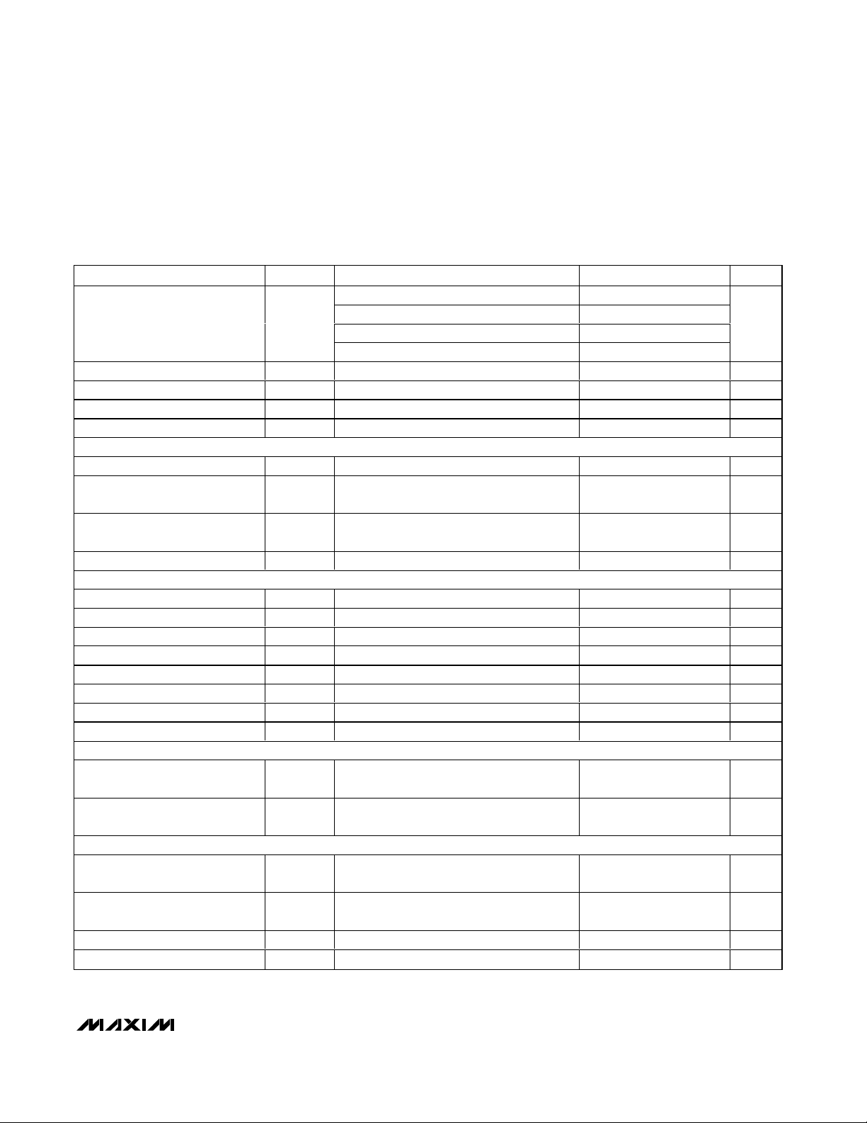
ELECTRICAL CHARACTERISTICS (continued)
(AVDD= DVDD= +5.0V, DRVDD= +3.0V, AGND = DGND = DRGND = 0, INTCLK/EXTCLK = AGND, f
CLK
= 5MHz, input range =
±10V, REFP2 = REFP1, REFN2 = REFN1, COM1 = COM2, 1.0nF from REFADC to AGND, 1.0µF and 0.1µF from COM1 to AGND,
0.1µF from REFP1 to AGND, 0.1µF from REFN1 to AGND, 1.0µF from REFP1 to REFN1. Typical values are at T
A
= +25°C. TA= T
MIN
to T
MAX
, unless otherwise noted.)
PARAMETER
CONDITIONS
UNITS
Range set bits = (0,0) -5 +5
Range set bits = (0,1)
Range set bits = (1,0)
Input Common-Mode Range
Range set bits = (1,1)
V
Input Resistance All settings
kΩ
Input Capacitance 15 pF
Small-Signal Bandwidth SSBW (Note 1) 1
MHz
Full-Power Bandwidth FPBW (Note 1) 75 kHz
INTERNAL REFERENCE (REFADC)
Output Voltage
2.5
V
Differential Reference Voltage
REFP–
REFN
2.5 V
Output-Voltage Temperature
Coefficient
50
ppm/°C
Load Regulation 5
V/mA
EXTERNAL REFERENCE
REFADC Voltage Input Range 2.0 2.5 3.0 V
REFADC Input Current (Note 3)
µA
REFADC Input Resistance R
REF
5kΩ
REFADC Input Capacitance 15 pF
TRACK/HOLD (T/H)
Aperture Delay t
AD
(Note 1) 16 ns
Aperture-Delay Matching
ps
Aperture Jitter t
AJ
(Note 1) 50
ps
RMS
CLOCK-SELECT INPUT (INTCLK/EXTCLK)
Input-Voltage High V
IH
0.7 x
V
Input-Voltage Low V
IL
0.3 x
V
DIGITAL INTERFACE AND CONTROL INPUTS (CS, RD, WR, CONVST, SHDN, CLK, STANDBY)
Input-Voltage High V
IH
0.7 x
V
Input-Voltage Low V
IL
0.3 x
V
Input Hysteresis 50 mV
Input Capacitance C
IN
15 pF
SYMBOL
MIN TYP MAX
-2.5 +2.5
-1.25 +1.25
-0.625 +0.625
2.475
-250 +250
AV
DRV
6.25
100
DD
DD
2.525
AV
DRV
DD
DD
Page 4
MAX1338
14-Bit, 4-Channel, Software-Programmable,
Multiranging, Simultaneous-Sampling ADC
4 _______________________________________________________________________________________
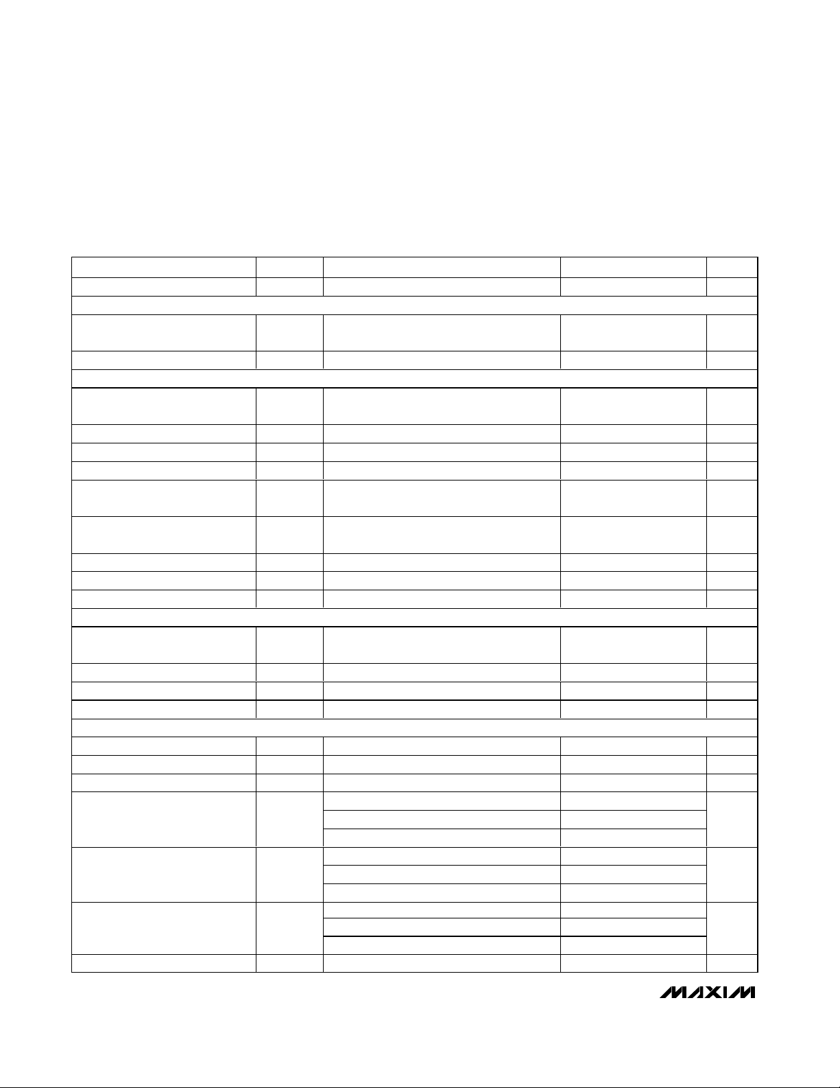
ELECTRICAL CHARACTERISTICS (continued)
(AVDD= DVDD= +5.0V, DRVDD= +3.0V, AGND = DGND = DRGND = 0, INTCLK/EXTCLK = AGND, f
CLK
= 5MHz, input range =
±10V, REFP2 = REFP1, REFN2 = REFN1, COM1 = COM2, 1.0nF from REFADC to AGND, 1.0µF and 0.1µF from COM1 to AGND,
0.1µF from REFP1 to AGND, 0.1µF from REFN1 to AGND, 1.0µF from REFP1 to REFN1. Typical values are at T
A
= +25°C. TA= T
MIN
to T
MAX
, unless otherwise noted.)
PARAMETER
CONDITIONS
UNITS
Input Current I
IN
VIN = 0 or DRV
DD
±1 µA
DIGITAL INTERFACE AND CONTROL OUTPUTS (EOC, EOLC)
Output-Voltage High V
OH
Sourcing 0.8mA
DRV
DD
V
Output-Voltage Low V
OL
Sinking 1.6mA 0.4 V
PARALLEL DIGITAL I/O (D0–D7)
Output-Voltage High V
OH
Sourcing 0.8mA
DRV
DD
-
0.6
V
Output-Voltage Low V
OL
Sinking 1.6mA 0.4 V
Leakage Current 1µA
Tristate Output Capacitance RD = 1 or CS = 1 15 pF
Input-Voltage High V
IH
0.7 x
V
Input-Voltage Low V
IL
0.3 x
V
Input Hysteresis 50 mV
Input Capacitance C
IN
15 pF
Input Current I
IN
VIN = 0 or DRV
DD
±1 µA
PARALLEL DIGITAL OUTPUTS (D8–D13)
Output-Voltage High V
OH
Sourcing 0.8mA
DRV
DD
-
0.6
V
Output-Voltage Low V
OL
Sinking 1.6mA 0.4 V
Leakage Current 1µA
Tristate Output Capacitance 15 pF
POWER SUPPLIES
Analog Supply Voltage AV
DD
5
V
Digital Supply Voltage DV
DD
5
V
Parallel Digital I/O Supply Voltage
DRV
DD
V
41 60
SHDN = 1
0.1Analog Supply Current AI
DD
STANDBY = 1, SHDN = 0 4.2 5
mA
3
SHDN = 1
Digital Supply Current DI
DD
STANDBY = 1, SHDN = 0
mA
3
SHDN = 1 0
Digital Driver Supply Current DRI
DD
STANDBY = 1, SHDN = 0 0
mA
Analog Power-Supply Rejection
4.75V to 5.25V (Note 1) 75 dB
SYMBOL
MIN TYP MAX
- 0.6
DRV
4.75
4.75
2.70 5.25
DD
0.005
0.001 0.05
0.001 0.05
DRV
5.25
5.25
0.05
0.05
DD
Page 5
MAX1338
14-Bit, 4-Channel, Software-Programmable,
Multiranging, Simultaneous-Sampling ADC
_______________________________________________________________________________________ 5
ELECTRICAL CHARACTERISTICS (continued)
(AVDD= DVDD= +5.0V, DRVDD= +3.0V, AGND = DGND = DRGND = 0, INTCLK/EXTCLK = AGND, f
CLK
= 5MHz, input range =
±10V, REFP2 = REFP1, REFN2 = REFN1, COM1 = COM2, 1.0nF from REFADC to AGND, 1.0µF and 0.1µF from COM1 to AGND,
0.1µF from REFP1 to AGND, 0.1µF from REFN1 to AGND, 1.0µF from REFP1 to REFN1. Typical values are at T
A
= +25°C. TA= T
MIN
to T
MAX
, unless otherwise noted.)
PARAMETER
CONDITIONS
UNITS
TIMING CHARACTERISTICS (Figures 4, 5, and 6)
Internal clock 2.9 3.2 3.5 µs
Time to First Conversion Result t
EOC1
External clock 16
CLK
Cycles
Internal clock 600 ns
Time to Subsequent Conversions
t
NEXT
External clock 3
CLK
Cycles
CONVST Pulse-Width Low
0.1 µs
CS Pulse Width t
CS
30 ns
RD Pulse-Width Low t
RDL
30 ns
RD Pulse-Width High t
RDH
30 ns
WR Pulse-Width Low t
WRL
30 ns
CS to WR Setup Time t
CTW
0ns
WR to CS Hold Time t
WTC
0ns
CS to RD Setup Time t
CTR
0ns
RD to CS Hold Time t
RTC
0ns
Data Access Time
(RD Low to Valid Data)
t
ACC
Figure 1 30 ns
Bus Relinquish Time
(RD High to D_ High-Z)
t
REQ
Figure 1 5 30 ns
CLK Rise to End-of-Conversion
(EOC) Rise/Fall Delay
t
EOCD
20 ns
CLK Rise to End-of-LastConversion (EOLC) Fall Delay
t
EOLCD
20 ns
CONVST Rise to EOLC Fall Delay
20 ns
Internal clock
200 ns
EOC Pulse-Width Low t
EOC
External clock 1
CLK
Cycle
Wake-Up Time From Standby 7µs
Wake-Up Time From Shutdown All bypass capacitors discharged 5 ns
SYMBOL
t
CONVST
MIN TYP MAX
t
CVEOLCD
180
Page 6
MAX1338
14-Bit, 4-Channel, Software-Programmable,
Multiranging, Simultaneous-Sampling ADC
6 _______________________________________________________________________________________
ELECTRICAL CHARACTERISTICS (continued)
(AVDD= DVDD= +5.0V, DRVDD= +3.0V, AGND = DGND = DRGND = 0, INTCLK/EXTCLK = AGND, f
CLK
= 5MHz, input range =
±10V, REFP2 = REFP1, REFN2 = REFN1, COM1 = COM2, 1.0nF from REFADC to AGND, 1.0µF and 0.1µF from COM1 to AGND,
0.1µF from REFP1 to AGND, 0.1µF from REFN1 to AGND, 1.0µF from REFP1 to REFN1. Typical values are at T
A
= +25°C. TA= T
MIN
to T
MAX
, unless otherwise noted.)
PARAMETER
SYMBOL
CONDITIONS
MIN
TYP
MAX
UNITS
EOC Fall to RD Fall Setup Time
0ns
0ns
Input Data Setup Time t
DTW
10 ns
Input Data Hold Time t
WTD
10 ns
External CLK Period t
CLK
200 ns
External CLK High Period t
CLKH
Logic sensitive to rising edges 60 ns
External CLK Low Period t
CLKL
Logic sensitive to rising edges 60 ns
External Clock Frequency f
CLK
(Note 4) 1 6
MHz
Internal Clock Frequency f
INT
5.0
5.5
MHz
CONVST High to CLK Edge t
CNTC
30 ns
Quiet Time t
QUIET
ns
Note 1: See definition for this parameter in the Definitions section.
Note 2: Differential reference voltage (REFP–REFN) error nulled.
Note 3: This is the load the MAX1338 presents to an external reference at REFADC.
Note 4: Minimum CLK frequency is limited only by the internal T/H droop rate. Limit the time between the rising edge of CONVST to
the falling edge of EOLC to a maximum of 0.25ms.
1.6V
1.6mA
0.8mA
50pF
TO OUTPUT PIN
Figure 1. Load Circuit for Data Access Time and BusRelinquish Time
t
EOCRD
EOLC Fall to RD Fall Setup Time t
EOLCRD
166
5.25
600
Page 7
MAX1338
14-Bit, 4-Channel, Software-Programmable,
Multiranging, Simultaneous-Sampling ADC
_______________________________________________________________________________________ 7
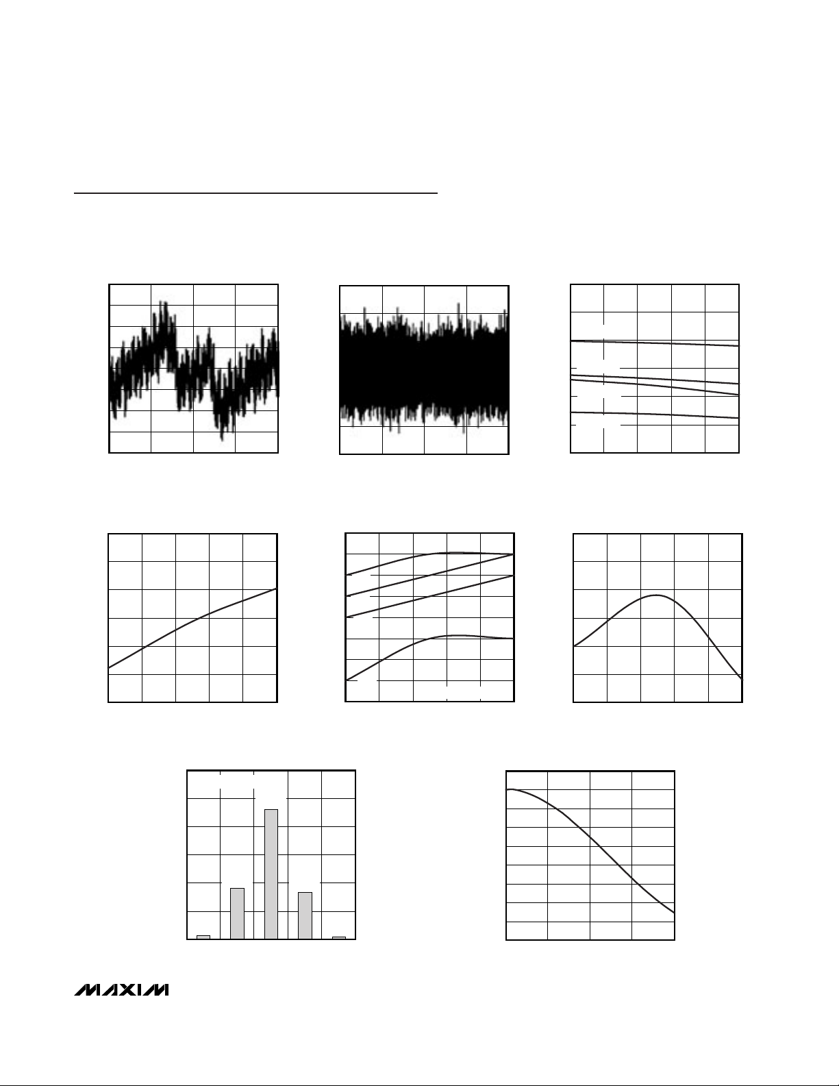
-0.8
-0.6
-0.4
-0.2
0
0.2
0.4
0.6
0.8
-8192 -4096 0 4096 8192
INTEGRAL NONLINEARITY
vs. OUTPUT CODE
MAX1338 toc01
OUTPUT CODE (DECIMAL)
INL (LSB)
-0.6
-0.2
-0.4
0.2
0
0.4
0.6
-8192 0-4096 4096 8192
DIFFERENTIAL NONLINEARITY
vs. OUTPUT CODE
MAX1338 toc02
OUTPUT CODE (DECIMAL)
DNL (LSB)
-6
-4
-5
-2
-3
-1
0
4.75 4.954.85 5.05 5.15 5.25
OFFSET ERROR
vs. SUPPLY VOLTAGE
MAX1338 toc03
AVDD (V)
OFFSET ERROR (LSB)
CHANNEL 0
CHANNEL 2
CHANNEL 1
CHANNEL 3
-15
-5
-10
5
0
10
15
-40 10-15 35 60 85
OFFSET ERROR
vs. TEMPERATURE
MAX1338 toc04
TEMPERATURE (°C)
OFFSET (LSB)
GAIN ERROR
vs. SUPPLY VOLTAGE
MAX1338 toc05
SUPPLY VOLTAGE (V)
GAIN ERROR (%FS)
5.155.054.85 4.95
-0.20
-0.19
-0.18
-0.17
-0.16
-0.15
-0.14
-0.13
-0.21
4.75 5.25
CH1
CH2
CH3
CH0
REFERENCE ERROR NULLED
-0.15
-0.05
-0.10
0.05
0
0.10
0.15
-40 10-15 35 60 85
GAIN ERROR
vs. TEMPERATURE
MAX1338 toc06
TEMPERATURE (°C)
GAIN ERROR (%FS)
0
2000
1000
4000
3000
5000
6000
-2 0-1 1 2
OUTPUT HISTOGRAM
(DC INPUT)
MAX1338 toc07
DIGITAL OUTPUT CODE
COUNTS
61
1646.25
4584.25
1802.75
97.25
OFFSET NORMALIZED
-0.8
-0.6
-0.5
-0.4
-0.3
-0.2
-0.1
0
0.1
050100 150 200
ANALOG INPUT BANDWIDTH
MAX1338 toc08
fIN (kHz)
ATTENUATION (dB)
-0.7
Typical Operating Characteristics
(AVDD= DVDD= +5.0V, DRVDD= +3.0V, AGND = DGND = DRGND = 0, INTCLK/EXTCLK = AGND, f
CLK
= 5MHz, input range =
±10V, REFP2 = REFP1, REFN2 = REFN1, COM1 = COM2, 1.0nF from REFADC to AGND, 1.0µF and 0.1µF from COM1 to AGND,
0.1µF from REFP1 to AGND, 0.1µF from REFN1 to AGND, 1.0µF from REFP1 to REFN1.)
Page 8
MAX1338
14-Bit, 4-Channel, Software-Programmable,
Multiranging, Simultaneous-Sampling ADC
8 _______________________________________________________________________________________
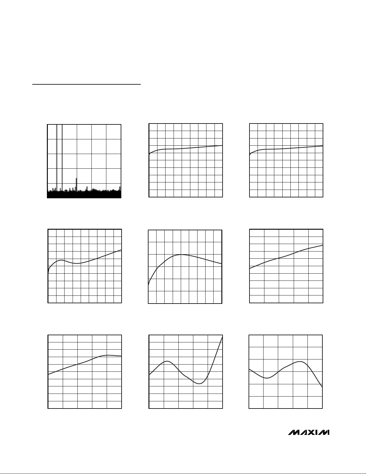
-125
-100
-50
-75
-25
0
03015 45 60 75
FFT AT f
SAMPLE
= 150ksps, fIN = 10kHz
MAX1338 toc10
FREQUENCY (kHz)
AMPLITUDE (dB)
70
72
71
74
73
76
75
77
79
78
80
1 3452 678910
SIGNAL-TO-NOISE RATIO
vs. CLOCK FREQUENCY
MAX1338 toc11
f
CLK
(MHz)
SNR (dB)
70
72
71
74
73
76
75
77
79
78
80
1 3452 678910
SIGNAL-TO-NOISE PLUS DISTORTION
vs. CLOCK FREQUENCY
MAX1338 toc12
f
CLK
(MHz)
SNR (dB)
-110
-106
-108
-102
-104
-98
-100
-96
-92
-94
-90
1 3452 678910
TOTAL HARMONIC DISTORTION
vs. CLOCK FREQUENCY
MAX1338 toc13
f
CLK
(MHz)
THD (dB)
80
85
90
95
100
105
110
13245678910
SPURIOUS-FREE DYNAMIC RANGE
vs. CLOCK FREQUENCY
MAX1338 toc14
f
CLK
(MHz)
SFDR (dB)
70
73
72
71
74
75
76
77
78
79
80
2.0 2.42.2 2.6 2.8 3.0
SIGNAL-TO-NOISE RATIO
vs. REFERENCE VOLTAGE
MAX1338 toc15
V
REFADC
(V)
SNR (dB)
70
73
72
71
74
75
76
77
78
79
80
2.0 2.42.2 2.6 2.8 3.0
SIGNAL-TO-NOISE PLUS DISTORTION
vs. REFERENCE VOLTAGE
MAX1338 toc16
V
REFADC
(V)
SINAD (dB)
-105
-99
-101
-103
-97
-95
-93
-91
-89
-87
-85
2.0 2.42.2 2.6 2.8 3.0
TOTAL HARMONIC DISTORTION
vs. REFERENCE VOLTAGE
MAX1338 toc17
V
REFADC
(V)
THD (dB)
80
90
85
100
95
105
110
2.0 2.42.2 2.6 2.8 3.0
SPURIOUS-FREE DYNAMIC RANGE
vs. REFERENCE VOLTAGE
MAX1338 toc18
V
REFADC
(V)
SFDR (dB)
Typical Operating Characteristics (continued)
(AVDD= DVDD= +5.0V, DRVDD= +3.0V, AGND = DGND = DRGND = 0, INTCLK/EXTCLK = AGND, f
CLK
= 5MHz, input range =
±10V, REFP2 = REFP1, REFN2 = REFN1, COM1 = COM2, 1.0nF from REFADC to AGND, 1.0µF and 0.1µF from COM1 to AGND,
0.1µF from REFP1 to AGND, 0.1µF from REFN1 to AGND, 1.0µF from REFP1 to REFN1.)
Page 9

MAX1338
14-Bit, 4-Channel, Software-Programmable,
Multiranging, Simultaneous-Sampling ADC
_______________________________________________________________________________________ 9
42.4
42.6
42.8
43.0
43.2
43.4
43.6
43.8
44.0
4.75 4.85 4.95 5.05 5.15 5.25
SUPPLY CURRENT
vs. SUPPLY VOLTAGE
MAX1338 toc19
AVDD (V)
A|
DD
+ D|
DD
(mA)
EXCLUDES DRIVER CURRENT
40
42
41
44
43
45
46
-40 10-15 35 60 85
SUPPLY CURRENT
vs. TEMPERATURE
MAX1338 toc20
TEMPERATURE (°C)
A|
DD
+ D|
DD
(mA)
EXCLUDES DRIVER CURRENT
0
0.5
1.0
1.5
2.0
2.5
3.0
3.5
4.0
2.75 3.25 3.75 4.25 4.75 5.25
DRIVER SUPPLY CURRENT
vs. SUPPLY VOLTAGE
MAX1338 toc21
DRVDD (V)
DR|
DD
(mA)
0.90
0.91
0.92
0.93
0.94
0.95
0.96
0.97
0.98
-40 -15 10 35 60 85
DRIVER SUPPLY CURRENT
vs. TEMPERATURE
MAX1338 toc22
TEMPERATURE (°C)
DR|
DD
(mA)
DRVDD = 3V
2.4978
2.4980
2.4979
2.4983
2.4982
2.4981
2.4986
2.4985
2.4984
2.4987
4.75 4.954.85 5.05 5.15 5.25
REFERENCE VOLTAGE
vs. SUPPLY VOLTAGE
MAX1338 toc23
AVDD (V)
V
REFADC
(V)
2.490
2.494
2.492
2.498
2.496
2.502
2.500
2.504
-40 10-15 35 60 85
REFERENCE VOLTAGE
vs. TEMPERATURE
MAX1338 toc24
TEMPERATURE (°C)
V
REFADC
(V)
40
50
45
60
55
65
70
4.75 4.954.85 5.05 5.15 5.25
SHUTDOWN CURRENT
vs. SUPPLY VOLTAGE
MAX1338 toc25
AVDD (V)
A|
DD
(µA)
SHDN = AV
DD
Typical Operating Characteristics (continued)
(AVDD= DVDD= +5.0V, DRVDD= +3.0V, AGND = DGND = DRGND = 0, INTCLK/EXTCLK = AGND, f
CLK
= 5MHz, input range =
±10V, REFP2 = REFP1, REFN2 = REFN1, COM1 = COM2, 1.0nF from REFADC to AGND, 1.0µF and 0.1µF from COM1 to AGND,
0.1µF from REFP1 to AGND, 0.1µF from REFN1 to AGND, 1.0µF from REFP1 to REFN1.)
Page 10

MAX1338
14-Bit, 4-Channel, Software-Programmable,
Multiranging, Simultaneous-Sampling ADC
10 ______________________________________________________________________________________
4.00
4.10
4.05
4.20
4.15
4.25
4.30
-40 10-15 35 60 85
STANDBY CURRENT
vs. TEMPERATURE
MAX1338 toc28
TEMPERATURE (°C)
A|
DD
(mA)
STANDBY = AV
DD
4.8
5.0
5.4
5.2
5.6
5.8
4.75 4.954.85 5.05 5.15 5.25
CONVERSION TIME
vs. SUPPLY VOLTAGE
MAX1338 toc29
AVDD (V)
CONVERSION TIME (µs)
INTERNAL CLOCK
4.8
5.0
5.4
5.2
5.6
5.8
-40 10-15 35 60 85
CONVERSION TIME
vs. TEMPERATURE
MAX1338 toc30
TEMPERATURE (°C)
CONVERSION TIME (µs)
INTERNAL CLOCK
-4
-3
-2
-1
0
1
2
3
4
-17.0 -8.5 0 8.5 17.0
ANALOG INPUT CURRENT
vs. ANALOG INPUT VOLTAGE
MAX1338 toc31
INPUT VOLTAGE (V)
INPUT CURRENT (mA)
Typical Operating Characteristics (continued)
(AVDD= DVDD= +5.0V, DRVDD= +3.0V, AGND = DGND = DRGND = 0, INTCLK/EXTCLK = AGND, f
CLK
= 5MHz, input range =
±10V, REFP2 = REFP1, REFN2 = REFN1, COM1 = COM2, 1.0nF from REFADC to AGND, 1.0µF and 0.1µF from COM1 to AGND,
0.1µF from REFP1 to AGND, 0.1µF from REFN1 to AGND, 1.0µF from REFP1 to REFN1.)
40
50
45
60
55
65
70
-40 10-15 35 60 85
SHUTDOWN CURRENT
vs. TEMPERATURE
MAX1338 toc26
TEMPERATURE (°C)
A|
DD
(µA)
SHDN = AV
DD
4.00
4.10
4.05
4.20
4.15
4.25
4.30
4.75 4.954.85 5.05 5.15 5.25
STANDBY CURRENT
vs. SUPPLY VOLTAGE
MAX1338 toc27
AVDD (V)
A|
DD
(mA)
STANDBY = AV
DD
Page 11

MAX1338
14-Bit, 4-Channel, Software-Programmable,
Multiranging, Simultaneous-Sampling ADC
______________________________________________________________________________________ 11
Pin Description
PIN NAME FUNCTION
1, 7, 9, 17,
19
AV
DD
Analog Power Input. AVDD is the power input for the analog section of the converter. Connect a
+4.75V to +5.25V power supply to AV
DD
. Bypass each AVDD to AGND with a 0.1µF capacitor very
close to the device. Bypass AV
DD
to AGND with a bulk capacitor of at least 4.7µF where power enters
the board. Connect all AV
DD
pins to the same potential.
2 AIN0+ Channel 0 Differential Analog Input
3 AIN0- Channel 0 Differential Analog Input
4 AIN1+ Channel 1 Differential Analog Input
5 AIN1- Channel 1 Differential Analog Input
6, 8, 14, 16,
18, 20, 28
AGND Analog Ground. AGND is the power return for AVDD. Connect all AGNDs to the same potential.
10 AIN2+ Channel 2 Differential Analog Input
11 AIN2- Channel 2 Differential Analog Input
12 AIN3+ Channel 3 Differential Analog Input
13 AIN3- Channel 3 Differential Analog Input
15
INTCLK/
EXTCLK
Clock-Select Input. Force INTCLK/EXTCLK high for internal clock mode. Force INTCLK/EXTCLK low
for external clock mode.
21 REFADC
ADC Reference Bypass or Input. REFADC is the bypass point for an internally generated reference
voltage. Bypass REFADC with a 1.0nF capacitor to AGND. REFADC can be driven externally by a
precision external voltage reference. See the Reference section and the Typical Operating Circuit.
22 REFP1 Positive Differential Reference Bypass Point 1. Connect REFP1 to REFP2.
23 REFP2
Positive Differential Reference Bypass Point 2. Connect REFP2 to REFP1. Bypass REFP2 with a 0.1µF
capacitor to AGND. Also bypass REFP2 to REFN2 with a 0.1µF capacitor.
24 COM1 Common-Mode Voltage Bypass Point 1. Connect COM1 to COM2.
25 COM2
Common-Mode Voltage Bypass Point 2. Connect COM2 to COM1. Connect a 1.0µF capacitor from
COM2 to AGND.
26 REFN1 Negative Differential Reference Bypass Point 1. Connect REFN1 to REFN2.
27 REFN2
Negative Differential Reference Bypass Point 2. Connect REFN2 to REFN1. Bypass REFN2 with a
0.1µF capacitor to AGND. Also bypass REFN2 to REFP2 with a 0.1µF capacitor.
29 D0 Data Input/Output Bit 0 (LSB)
30 D1 Data Input/Output Bit 1
31 D2 Data Input/Output Bit 2
32 D3 Data Input/Output Bit 3
33 D4 Data Input/Output Bit 4
34 D5 Data Input/Output Bit 5
35 D6 Data Input/Output Bit 6
36 D7 Data Input/Output Bit 7
37 D8 Data Output Bit 8
38 D9 Data Output Bit 9
39 D10 Data Output Bit 10
40 D11 Data Output Bit 11
Page 12

MAX1338
Detailed Description
The MAX1338 simultaneously samples four differential
analog inputs with internal T/H circuits, and sequentially
converts them to a digital code with a 14-bit ADC.
Output data is provided by a 14-bit parallel interface. At
power-up, all channels default to a ±10V input range.
Program different input ranges (±10V, ±5V, ±2.5V, or
±1.25V) using the configuration register. Different input
ranges between ±12V and ±1.0V are realized using an
external reference. All channels offer input protection to
±17V, independent of the selected input range.
The internal clock operates the ADC at 5MHz, or uses
an external conversion clock from 1MHz to 6MHz. EOC
goes low when the result of each conversion is available, and EOLC goes low when the last conversion
result is available. Standby and shutdown modes,
selectable through logic-control inputs, save power
between conversions. Figure 2 shows a block diagram
of the MAX1338.
14-Bit, 4-Channel, Software-Programmable,
Multiranging, Simultaneous-Sampling ADC
12 ______________________________________________________________________________________
Pin Description (continued)
PIN NAME FUNCTION
41 D12 Data Output Bit 12
42 D13 Data Output Bit 13 (MSB)
43 DRV
DD
Digital I/O Power-Supply Input. DRVDD is the power input for the digital I/O buffers and drivers.
Connect a +2.7V to +5.25V power supply to DRV
DD
. Bypass DRVDD to DRGND with a 0.1µF
capacitor very close to the device.
44 DRGND Driver Ground. DRGND is the power-supply return for DRVDD.
45 EOC
End-of-Conversion Output. EOC goes low to indicate the end of a conversion. EOC returns high after
one clock period.
46 EOLC
End-of-Last-Conversion Output. EOLC goes low to indicate the end of the last conversion. EOLC
returns high when CONVST goes low for the next conversion sequence.
47 RD
Read Input. Forcing RD low initiates a read command of the parallel data bus, D0–D13. D0–D13 are
high impedance while either RD or CS is high.
48 WR Write Input. Forcing WR low initiates a write command for configuring the device through D0–D7.
49 CS
Chip-Select Input. Forcing CS low activates the digital interface. D0–D13 are high impedance while
either CS or RD is high.
50 CONVST
Convert Start Input. CONVST initiates the conversion process. The analog inputs are sampled on the
rising edge of CONVST.
51 CLK
External-Clock Input. CLK accepts a 1MHz to 6MHz external clock signal. For externally clocked
conversions, apply the clock signal to CLK and force INTCLK/EXTCLK low. For internally clocked
conversions, connect CLK to DGND and force INTCLK/EXTCLK high.
52
Standby-Control Input. Forcing STANDBY high partially powers down the device but leaves all the
reference-related circuitry alive. Use STANDBY instead of SHDN when quick wake-up is required.
53 SHDN
Shutdown-Control Input. Force SHDN high to place the device into full shutdown. When in full
shutdown, all circuitry within the device is powered down and all reference capacitors are allowed to
discharge. Allow 1ms for wake-up from full shutdown before starting a conversion.
54 DV
DD
D i g i tal P ow er - S up p l y Inp ut. D V
D D
i s the p ow er i np ut for the d i g i tal ci r cui tr y. C onnect a + 4.75V to + 5.25V
p ow er sup p l y to D V
D D
. Byp ass D V
D D
to D GN D w i th a 0.1µF cap aci tor ver y cl ose to the d evi ce.
55, 56 DGND Digital Ground. Power return for DVDD.
—EPExposed Pad. Connect to AGND.
STANDBY
Page 13

Power-Supply Inputs
Three separate power supplies power the MAX1338. A
+5V analog supply, AVDD, powers the analog input and
converter sections. A +5V digital supply, DVDD, powers
the internal logic circuitry, and a +2.7V to +5V digital
supply (DRVDD), powers the parallel I/O and the control
I/O (see the Typical Operating Circuit). Bypass the
power supplies as indicated in the Layout, Grounding,
and Bypassing section. Power-supply sequencing is
not required for the MAX1338.
Analog Inputs
Software-Selectable Input Range
The MAX1338 provides four independent, softwareselectable, analog input voltage ranges for each channel. The selectable input ranges are ±V
REF
x 4 (the
power-up default condition), ±V
REF
x 2, ±V
REF
, and
±V
REF
x 0.5. Using the 2.5V internal reference, the
selectable input ranges are ±10V (power-up default),
±5V, ±2.5V, and ±1.25V. Program the analog input
ranges with the configuration register through the
parallel I/O. See the Configuration Register section for
programming details.
Input Protection
Protection at the analog inputs provides ±17V fault
immunity for the MAX1338. This protection circuit limits
the current at the analog inputs to less than ±2mA.
Input fault protection is active in standby, in shutdown,
during normal operation, and over all input ranges.
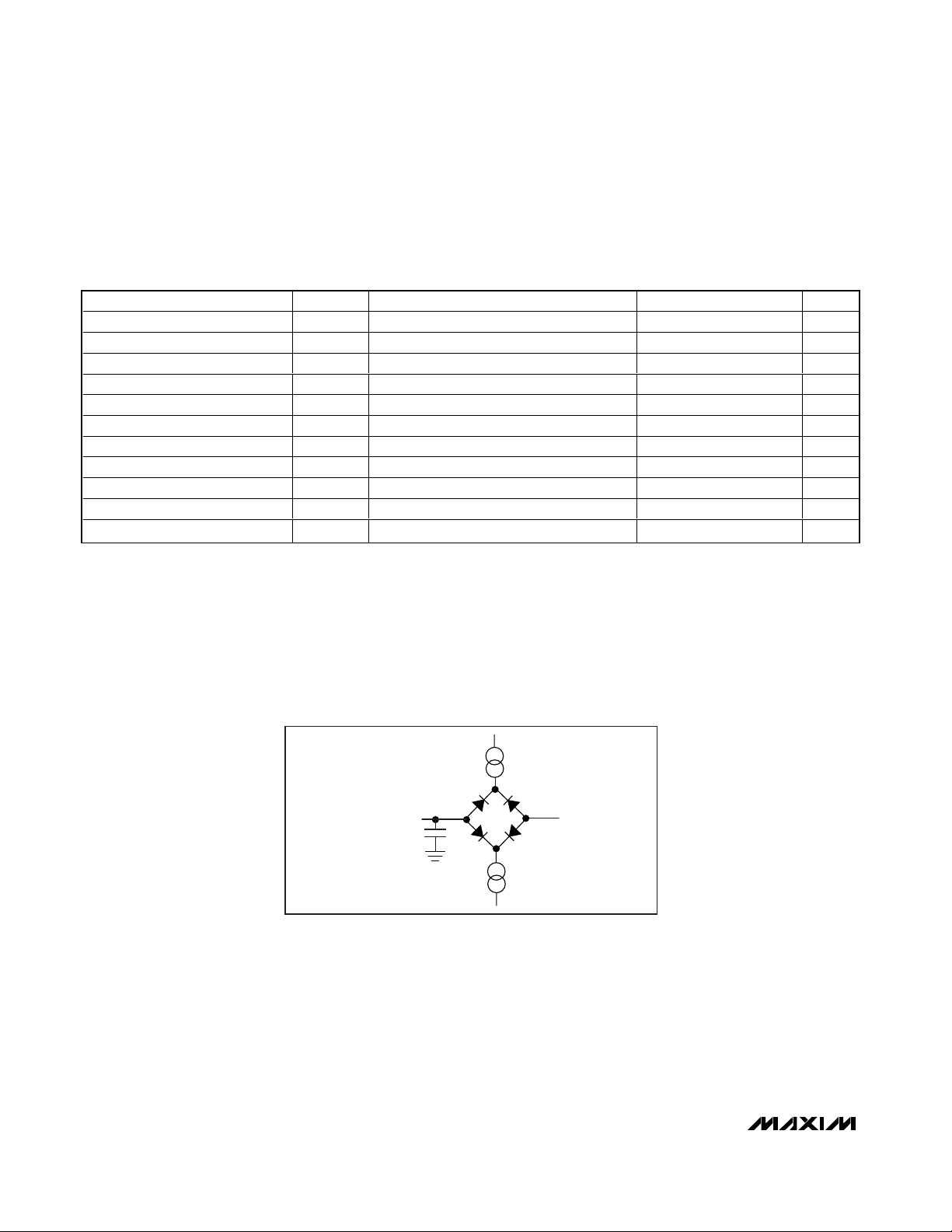
Track and Hold (T/H)
To preserve relative phase information between input
channels, each input channel has a dedicated T/H
amplifier. The rising edge of CONVST represents the
sampling instant for all channels. All samples are taken
within an aperture delay (tAD) of 16ns. The aperture
delay of all channels is matched to within 100ps.
MAX1338
14-Bit, 4-Channel, Software-Programmable,
Multiranging, Simultaneous-Sampling ADC
______________________________________________________________________________________ 13
MAX1338
CONVST
D13
DGND
AV
DD
SHDN
CLK
INTERFACE
AND
CONTROL
14-BIT
ADC
D0
DV
DD
AGND
STANDBY
REFADC
S/H
4 x 14
SRAM
OUTPUT
DRIVERS
5kΩ
2.500V
INTCLK/EXTCLK
CS
RD
EOC
EOLC
REFN1
DRGND
WR
DRV
DD
D8
D7
CONFIGURATION
REGISTER
REFN2
COM1
COM2
REFP2
REFP1
AIN3+
AIN3-
S/H
AIN0-
AIN0+
4 x 1
MUX
Figure 2. Functional Diagram
Page 14

MAX1338
Figure 3 shows the equivalent analog input T/H circuit
for one analog input.
As conversion begins, the T/H circuits hold the analog
signals. After the 12th clock cycle (or 2.4µs in internal
clock mode) into the conversion process, the last analog input sample begins shifting through the converter,
and the T/H circuits begin to track the analog inputs
again in preparation for the next CONVST rising edge.
Due to the resistive load presented by the analog
inputs, any significant analog input source resistance,
R
SOURCE
, increases gain error. Limit R
SOURCE
to a
maximum of 20Ω to limit the effect to less than 0.1%.
Drive the input with a wideband buffer (>1MHz) that
can drive the ADC’s input impedance.
Selecting an Input Buffer
Most applications require an input buffer to achieve 14bit accuracy. Although slew rate and bandwidth are
important, the most critical specification is output impedance. Use a low-noise, low-distortion amplifier with low
output impedance, for best gain-accuracy performance.
Input Bandwidth
The input-tracking circuitry has a 1MHz small-signal
bandwidth. To avoid high-frequency signals being
aliased into the frequency band of interest, anti-alias filtering is recommended.
Data Throughput
The data throughput (fTH) of the MAX1338 is a function
of the clock speed (f
CLK
). The MAX1338 operates from
a 5MHz internal clock or an external clock between
1MHz and 6MHz. For fastest throughput, read the conversion result during conversion (Figure 5), and calculate data throughput using:
where t
QUIET
is the period of bus inactivity before the
rising edge of CONVST.
Clock Modes
The MAX1338 provides an internal clock of 5MHz.
Alternatively, use an external clock of 1MHz to 6MHz.
Internal Clock
Internal clock mode frees the microprocessor from the
burden of running the ADC conversion clock. For internal-clock operation, connect INTCLK/EXTCLK to AV
DD
and CLK to DRGND. Note that INTCLK/EXTCLK is referenced to the analog power supply, AVDD. Total conversion time for all four channels using the internal
clock is 6µs (typ).
f
t
f
TH
QUIET
CLK
=
+
1
26
14-Bit, 4-Channel, Software-Programmable,
Multiranging, Simultaneous-Sampling ADC
14 ______________________________________________________________________________________
AIN_
R1
MAX1338
R2
1.9V
R1 || R2 = 6.25kΩ
C
HOLD
Figure 3. Simplified Typical Input Circuit
t
CS
t
CTW
t
WRL
t
WTC
t
DTW
DATA
IN
t
WTD
CONVST
CONFIGURATION
REGISTER ACTIVATES
RD
CS
WR
D0–D7
Figure 4. Write Timing
Page 15

External Clock
For external clock operation, force INTCLK/EXTCLK low
and connect an external clock source to CLK. Use an
external clock frequency from 1MHz to 6MHz with a
duty cycle between 40% and 60%. Choose a minimum
clock frequency of 1MHz to prevent linearity errors
caused by excessive droop in the T/H circuits.
Applications Sections
Power-On Reset
At power-up, all channels default to a ±10V input range.
After applying power, allow a 1ms wake-up time to
elapse and perform one dummy conversion before
initiating first conversion.
Power Saving
Full Shutdown
During shutdown, the analog and digital circuits in the
MAX1338 power down and the device draws less than
0.06mA from AVDD, and less than 10µA from DVDD.
Select shutdown mode using the SHDN input. Force
SHDN high to enter shutdown mode. When coming out of
shutdown, allow the 1ms wake-up and then perform one
dummy conversion before making the first conversion.
Standby
Standby is similar to shutdown but the reference circuits remain powered up, allowing faster wake-up.
Enter standby by forcing STANDBY high. After coming
out of standby, perform a dummy conversion before
making the first conversion.
Digital Interface
The digital interface consists of two sections: a control
I/O section and a parallel I/O section. The control I/O
section includes the following control signals: chip
select (CS), read (RD), write (WR), end of conversion
(EOC), end of last conversion (EOLC), convert start
(CONVST), power-down (SHDN), standby (STANDBY),
and external-clock input (CLK).
The bidirectional parallel I/O section sets the 8-bit input
range configuration register using D0–D7 (see the
Configuration Register section) and outputs the 14-bit
conversion result using D0–D13. The I/O operations are
controlled by the control I/O signals RD, WR, and CS. All
parallel I/O bits are high impedance when either RD = 1
or CS = 1. Figures 4, 5, and 6 and the Timing Character-
istics section detail the operation of the digital interface.
Configuration Register
The MAX1338 uses an 8-bit configuration word to set the
input range for each channel. Table 1 and Table 2 describe
the configuration word and the input-range settings.
Write to the configuration register by forcing CS and WR
low, loading bits D0–D7 onto the parallel bus, and then
forcing WR high. The configuration bits are latched on
the rising edge of WR (Figure 4). It is possible to write to
the configuration register at any point during the conversion sequence. However, it will not be active until the
next convert-start signal. At power-up, the configuration
register contains all zeros, making all channels default to
the maximum input range, -10V to +10V. Shutdown and
standby do not change the configuration register, but
the configuration register can be programmed while the
MAX1338 is in shutdown or standby modes.
MAX1338
14-Bit, 4-Channel, Software-Programmable,
Multiranging, Simultaneous-Sampling ADC
______________________________________________________________________________________ 15
I/O LINE
REGISTER
NAME
FUNCTION
D0 CH0R0 Channel 0 input range setting bit 0
D1 CH0R1 Channel 0 input range setting bit 1
D2 CH1R0 Channel 1 input range setting bit 0
D3 CH1R1 Channel 1 input range setting bit 1
D4 CH2R0 Channel 2 input range setting bit 0
D5 CH2R1 Channel 2 input range setting bit 1
D6 CH3R0 Channel 3 input range setting bit 0
D7 CH3R1 Channel 3 input range setting bit 1
Table 1. Configuration Register
REGISTER
SETTING
CH_R0
SELECTED INPUT
RANGE
ALLOWABLE
COMMON-MODE
RANGE
00-10V to +10V ±5V
01 -5V to +5V ±2.5V
10-2.5V to +2.5V ±1.25V
11
±0.625V
Table 2. Input-Range Register Settings
CH_R1
-1.25V to +1.25V
Page 16

MAX1338
Starting a Conversion
Internal Clock
For internal clock operation, force INTCLK/EXTCLK
high. To start a conversion using internal clock mode,
pull CONVST low for at least t
CONVST
. The T/H acquires
the signal while CONVST is low. An EOC signal pulses
low when the first result becomes available, and for
each subsequent result until the end of the conversion
cycle. The EOLC signal goes low when the last conversion result becomes available (Figure 6).
External Clock
For external clock operation, force INTCLK/EXTCLK
low. To start a conversion using external clock mode,
pull CONVST low for at least t
CONVST
. The T/H circuits
track the input signal while CONVST is low. Conversion
begins on the rising edge of CONVST. Apply an external clock to CLK. To avoid T/H droop degrading the
sampled analog input signals, the first CLK pulse must
occur within 10µs after the rising edge of CONVST and
have a minimum 1MHz clock frequency. The first conversion result is available for read on the rising edge of
the 17th clock cycle, and subsequent conversions on
every 3rd clock cycle thereafter, as indicated by EOC
and EOLC.
Reading a Conversion Result
Reading During a Conversion
Figure 5 shows the interface signals to initiate a read
operation during a conversion cycle. CS can be held
low permanently, low during the RD cycles, or it can be
the same as RD. After initiating a conversion by bringing CONVST high, wait for EOC to go low (about 3.4µs
in internal clock mode) or 17 clock cycles (external
clock mode) before reading the first conversion result.
Read the conversion result by bringing RD low, which
latches the data to the parallel digital output bus. Bring
RD high to release the digital bus. Wait for the next
falling edge of EOC (about 600ns in internal clock
mode or three clock cycles in external clock mode)
before reading the next result. When the last result is
available, EOLC goes low, along with EOC. Wait three
clock cycles, t
QUIET
, before starting the next conver-
sion cycle.
Reading After a Conversion
Figure 6 shows the interface signals for a read operation
after a conversion using an external clock. At the falling
of EOLC, on the 26th clock pulse after the initiation of a
conversion, driving CS and RD low places the first conversion result onto the parallel I/O bus. Read the conversion result on the rising edge of RD. Successive low
pulses of RD place the successive conversion results
14-Bit, 4-Channel, Software-Programmable,
Multiranging, Simultaneous-Sampling ADC
16 ______________________________________________________________________________________
CONVST
17 18 19 20 21 22
23
24
25 26
27
29
t
QUIET
CH3
CH2
CH1
CH0
t
ACC
t
REQ
t
CONVST
SAMPLE
CLK
t
EOC1
t
NEXT
t
EOC
EOC
EOLC
RD
D0–D13
t
RDL
Figure 5. Reading During a Conversion—Internal or External Clock
Page 17

onto the bus. After reading all four channels, bring CS
high to release the parallel I/O. After waiting t
QUIET
,
pulse CONVST low to initiate the next conversion.
Reference
Bypass the reference inputs as indicated in Table 3.
Internal Reference
The internal reference supports all input ranges for the
MAX1338.
External Reference
Implement external-reference operation by overdriving
the internal reference voltage. Override the internal reference voltage by connecting a 2.0V to 3.0V external
reference at REF. The REF input impedance is typically
5kΩ. For more information about using an external reference, see the Transfer Functions section.
Transfer Functions
Digital Correction
Factory trim procedures digitally shift the transfer function to reduce bipolar zero-code offset to less than
±4 LSBs (typ). Depending on initial conditions, the
transfer function is shifted up or down, as required. The
maximum shift that any transfer function experiences is
64 codes, which can have a small effect at the
extremes of the transfer function, as shown in Figure 7.
MAX1338
14-Bit, 4-Channel, Software-Programmable,
Multiranging, Simultaneous-Sampling ADC
______________________________________________________________________________________ 17
CONVST
1
29
26
31
CH3
CH2
CH1
CH0
t
ACC
t
CONVST
SAMPLE
CLK
t
EOC
EOC
EOLC
D0–D13
2
27 28
30
t
CLKH
t
CLKL
t
CNTC
t
CLK
ONLY LAST PULSE SHOWN
CS
t
QUIET
t
RTC
t
RDH
t
RDL
t
CTR
t
EOCRD
t
EOLCRD
RD
t
REQ
Figure 6. Reading After a Conversion—External Clock
LOCATION
BYPASS
CAPACITORS
REFADC bypass capacitor to AGND 1nF
REFP1 bypass capacitor to AGND 0.1µF
REFN1 bypass capacitor to AGND 0.1µF
REFP1 to REFN1 capacitor 1.0µF
COM1 bypass capacitor to AGND 1.0µF || 0.1µF
Table 3. Reference Bypass Capacitors
Page 18

MAX1338
Input Range Settings
Table 4 shows the two’s complement output for a selection of inputs.
The full-scale input range (FSR) depends on the selected range, and the voltage at REF, as shown in Table 5.
Also shown in Table 5 are the allowable common-mode
ranges for the differential inputs.
Calculate the LSB size using:
where A = gain multiplier for the selected input range,
from Table 6.
Determine the input voltage as a function of V
REF
, and
the output code using:
where A = gain multiplier for the selected input range,
from Table 6.
Figures 8, 9, 10, and 11 show the transfer functions for
the four selectable input ranges.
Applications Information
Layout, Grounding, and Bypassing
For best performance, the board layout must follow
some simple guidelines. Separate the control I/O and
parallel I/O signals from the analog signals, and run the
clock signals separate from everything. Do not run analog and digital (especially clock) lines parallel to one
another, or digital lines underneath the ADC package.
Run the parallel I/O signals together as a bundle.
The MAX1338 has an exposed underside pad for a
low-inductance ground connection and low thermal
resistance. Connect the exposed pad to the circuit
board ground plane. Figure 12 shows the recommended system ground connections. Establish an analog
ground point at AGND and a digital ground point at
DGND. Connect all analog grounds to the analog
ground point. Connect all digital grounds to the digital
ground point. For lowest noise operation, make the
power-supply ground returns as low impedance and as
short as possible. Connect the analog ground point to
the digital ground point at one location.
High-frequency noise in the power supplies degrades
the ADC’s performance. Bypass AVDDto AGND with a
parallel combination of 0.1µF and 2.2µF capacitors,
bypass DVDDto DGND with a parallel combination of
0.1µF and 2.2µF capacitors, and bypass DRVDDto
DRGND with a parallel combination of 0.1µF and 2.2µF
capacitors. If the supply is very noisy use a ferrite bead
as a lowpass filter, as shown in Figure 12.
VVV A
CODE
AIN AIN REFADC__+ −
− =××
2
14
1
2
14
LSB
AV
REFADC
=
×
14-Bit, 4-Channel, Software-Programmable,
Multiranging, Simultaneous-Sampling ADC
18 ______________________________________________________________________________________
MAXIMUM
64 CODES
+8191
0-8192
0x2000
0x0000
0x1FFF
OUTPUT CODE
ADJUSTED
TRANSFER
FUNCTION
INITIAL
TRANSFER
FUNCTION
INPUT VOLTAGE (LSBs)
Figure 7. Example of Digitally Adjusted Transfer Function—
Shifted Down to Minimize Zero-Code Offset
8 x V
REFADC
8 x V
REF
2
14
1 LSB =
TWO'S COMPLEMENT BINARY OUTPUT CODE
-8192 -8190 +8191+8189
0x2000
0x2001
0x2002
0x2003
0x1FFF
0x1FFE
0x1FFD
0x1FFC
0x3FFF
0x0000
0x0001
0
INPUT VOLTAGE (V
AIN_+
- V
AIN_-
IN LSBs)
-1 +1
Figure 8. ±10V Transfer Function
Page 19

Definitions
Integral Nonlinearity (INL)
Integral nonlinearity is the deviation of the values on an
actual transfer function from a straight line. For these
devices, this straight line is a line drawn between the
endpoints of the transfer function, once offset and gain
errors have been nulled.
Differential Nonlinearity (DNL)
Differential nonlinearity is the difference between an
actual step width and the ideal value of 1 LSB. For
these devices, the DNL of each digital output code is
measured and the worst-case value is reported in the
Electrical Characteristics table. A DNL error specification of less than ±1 LSB guarantees no missing codes
and a monotonic transfer function.
Offset Error
Offset error indicates how well the actual transfer function matches the ideal transfer function at a single point.
Typically, the point at which the offset error is specified
is at or near the zero scale of the transfer function or at
or near the midscale of the transfer function.
For the MAX1338, the ideal zero-scale digital output
transition from 0x3FFF to 0x0000 occurs with an analog
input voltage of zero. Offset error is the amount of analog input-voltage deviation between the measured input
voltage and the calculated input voltage at the zeroscale transition.
MAX1338
14-Bit, 4-Channel, Software-Programmable,
Multiranging, Simultaneous-Sampling ADC
______________________________________________________________________________________ 19
INPUT VOLTAGE (V)
±10V INPUT
RANGE
SELECTED
±5V INPUT
RANGE
SELECTED
±2.5V INPUT
RANGE
SELECTED
±1.25V INPUT
RANGE
SELECTED
DECIMAL
EQUIVALENT
OUTPUT
(CODE
10
)
TWO’S COMPLEMENT
BINARY OUTPUT CODE
9.9988 4.9994 2.4998 1.2499 8191
01 1111 1111 1111 → 0x1FFF
9.9976 4.9988 2.4997 1.2498 8190
01 1111 1111 1110 → 0x1FFE
0.0012 0.0006 0.0002 0.0001 1
00 0000 0000 0001 → 0x0001
0000 0
00 0000 0000 0000 → 0x0000
-0.0012 -0.0006 -0.0002 -0.0001 -1
11 1111 1111 1111 → 0x3FFF
-9.9988 -4.9994 -2.4998 -1.2499 -8191
10 0000 0000 0001 → 0x2001
-10.0000 -5.0000 -2.5000 -1.2500 -8192
10 0000 0000 0000 → 0x2000
Table 4. Code Table with V
REF
= 2.500V
SELECTED
INPUT
RANGE (V)
V
REFADC
(V)
FULL-SCALE
INPUT RANGE
(V)
ALLOWABLE
COMMON-MODE
RANGE (V)
2.0 ±8 ±5
2.5 ±10 ±5±10
3.0 ±12 ±5
2.0 ±4 ±2.5
2.5 ±5 ±2.5±5
3.0 ±6 ±2.5
2.0 ±2 ±1.25
2.5 ±2.5 ±1.25
±2.5
3.0 ±3 ±1.25
2.0 ±1 ±0.625
2.5 ±1.25 ±0.625±1.25
3.0 ±1.5 ±0.625
Table 5. Input Ranges
SELECTED
INPUT RANGE
(V)
GAIN MULTIPLIER
(A)
LSB SIZE (mV)
±10 8 1.2207
±5 4 0.6104
±2.5 2 0.1526
±1.25 1 0.0736
Table 6. LSB Size with V
REF
= 2.500V
Page 20

MAX1338
Gain Error
Gain error indicates how well the slope of the actual
transfer function matches the slope of the ideal transfer
function. For the MAX1338, the gain error is the difference between the measured positive full-scale and
negative full-scale transition points minus the difference
between the ideal positive full-scale and negative fullscale bipolar transition points.
Signal-to-Noise Ratio (SNR)
SNR is a measure of the converter’s noise characteristics. For a waveform perfectly reconstructed from digital samples, SNR is the ratio of the full-scale analog
input (RMS value) to the RMS quantization error (residual error). The ideal, theoretical minimum analog-to-digital noise is caused by quantization noise error only and
results directly from the ADC’s resolution (N bits):
14-Bit, 4-Channel, Software-Programmable,
Multiranging, Simultaneous-Sampling ADC
20 ______________________________________________________________________________________
4 x V
REFADC
4 x V
REF
2
14
1 LSB =
TWO'S COMPLEMENT BINARY OUTPUT CODE
-8192 -8190 +8191+8189
0x2000
0x2001
0x2002
0x2003
0x1FFF
0x1FFE
0x1FFD
0x1FFC
0x3FFF
0x0000
0x0001
0
INPUT VOLTAGE (V
AIN_+
- V
AIN_-
IN LSBs)
-1 +1
Figure 9. ±5V Transfer Function
2 x V
REFADC
2 x V
REF
2
14
1 LSB =
TWO'S COMPLEMENT BINARY OUTPUT CODE
-8192 -8190 +8191+8189
0x2000
0x2001
0x2002
0x2003
0x1FFF
0x1FFE
0x1FFD
0x1FFC
0x3FFF
0x0000
0x0001
0
INPUT VOLTAGE (V
AIN_+
- V
AIN_-
IN LSBs)
-1 +1
Figure 10. ±2.5V Transfer Function
V
REFADC
V
REF
2
14
1 LSB =
TWO'S COMPLEMENT BINARY OUTPUT CODE
-8192 -8190 +8191+8189
0x2000
0x2001
0x2002
0x2003
0x1FFF
0x1FFE
0x1FFD
0x1FFC
0x3FFF
0x0000
0x0001
0
INPUT VOLTAGE (V
AIN_+
- V
AIN_-
IN LSBs)
-1 +1
Figure 11. ±1.25V Transfer Function
DIGITAL POWER SUPPLIES
AV
DD
AGND
DGND
+5V
DIGITAL
CIRCUITS
FERRITE
BEAD
+5V
DV
DD
GND
MAX1338
+5V
+3V
GND
AGND
ANALOG
POWER SUPPLY
DRV
DD
DRGND
Figure 12. Power-Supply Grounding and Bypassing
Page 21

SNR = (6.02 x N + 1.76)dB
where N = 14 bits. In reality, there are other noise
sources such as thermal noise, reference noise, and
clock jitter. SNR is computed by taking the ratio of the
RMS signal to the RMS noise. RMS noise includes all
spectral components to the Nyquist frequency excluding the fundamental, the first five harmonics, and the
DC offset.
Signal-to-Noise Plus Distortion (SINAD)
SINAD indicates the converter’s noise and distortion
performance.
SINAD is computed by taking the ratio of the RMS signal to the RMS noise plus distortion. RMS noise plus
distortion includes all spectral components to the
Nyquist frequency excluding the fundamental and the
DC offset.
Effective Number of Bits (ENOB)
ENOB specifies the global accuracy of an ADC at a specific input frequency and sampling rate. An ideal ADC’s
error consists of quantization noise only. ENOB for a fullscale sinusoidal input waveform is computed from:
Total Harmonic Distortion (THD)
THD is a dynamic indication of how much harmonic
distortion the converter adds to the signal.
THD is the ratio of the RMS sum of the first five harmonics of the fundamental signal to the fundamental itself.
This is expressed as:
where V1is the fundamental amplitude and V2–V6are
the amplitudes of the 2nd- through 6th-order harmonics.
Spurious-Free Dynamic Range (SFDR)
SFDR is the ratio of the RMS amplitude of the fundamental (maximum signal component) to the RMS value
of the next largest spurious component, excluding DC
offset. SFDR is specified in decibels relative to the carrier (dBc).
Aperture Delay
Aperture delay (tAD) is the time delay from the sampling
clock edge to the instant when an actual sample is taken.
Aperture Jitter
Aperture jitter (tAJ) is the sample-to-sample variation in
aperture delay.
Channel-to-Channel Isolation
Channel-to-channel isolation indicates how well each
analog input is isolated from the others. The channel-tochannel isolation for the MAX1338 is measured by
applying a DC -0.5dBFS sine wave to the ON channel
while a high frequency 10kHz -0.5dBFS sine wave is
applied to all OFF channels. An FFT is taken for the ON
channel. From the FFT data, channel-to-channel
crosstalk is expressed in dB as the power ratio of the
DC signal applied to the ON channel and the high-frequency crosstalk signal from the OFF channels.
Power-Supply Rejection (PSRR)
PSRR is defined as the shift in gain error when the analog power supply is changed from 4.75V to 5.25V.
Small-Signal Bandwidth
A -20dBFS sine wave is applied to the MAX1338 input.
The frequency is increased until the amplitude of the
digitized conversion result decreases 3dB.
Full-Power Bandwidth
A -0.5dBFS sine wave is applied to the MAX1338 input.
The frequency is increased until the amplitude of the
digitized conversion result decreases 3dB.
THD
VVVVV
V
log =×
++++
20
2
232
4
2
5
262
1
ENOB
SINAD
.
.
=
− 176
602
SINAD dB
SIGNAL
NOISE DISTORTION
RMS
RMS
() log
( )
=×
+
20
MAX1338
14-Bit, 4-Channel, Software-Programmable,
Multiranging, Simultaneous-Sampling ADC
______________________________________________________________________________________ 21
Page 22

MAX1338
14-Bit, 4-Channel, Software-Programmable,
Multiranging, Simultaneous-Sampling ADC
22 ______________________________________________________________________________________
MAX1338
AIN3-
AIN0+
AIN0-
AIN1+
AIN1-
AIN2+
AIN2-
AIN3+
D12
D0
D1
D2
D3
D4
D5
D6
D7
D8
D9
D10
D11
AV
DD
AGND
DV
DD
DGND
AV
DD
AV
DD
REFADC
REFP1
COM1
+5V
GND
+5V
GND
D13
WR
RD
ANALOG
INPUTS
PARALLEL I/O
CS
EOLC
CONTROL I/O
13
12
11
10
5
4
3
2
6, 8, 14, 16, 18, 20, 28
27
23
21
53
51
50
54
49
48
47
46
45
52
42
41
40
39
38
37
36
35
34
33
32
31
30
29
55, 56
15
AV
DD
AV
DD
7
1
0.1µF
0.1µF
0.1µF
1.0µF
0.001µF
0.1µF
INTCLK/EXTCLK
SHDN
CLK
CONVST
EOC
STANDBY
DIGITAL
I/O
DIGITAL
OUTPUT
+3V TO +5V
GND
0.1µF
44
43
DRGND
DRV
DD
26
24
25
1.0µF
0.1µF
22
0.1µF
0.1µF
0.1µF
0.1µF
9
17
19
REFP2
REFN2
REFN1
COM2
Typical Operating Circuit
Page 23

MAX1338
14-Bit, 4-Channel, Software-Programmable,
Multiranging, Simultaneous-Sampling ADC
______________________________________________________________________________________ 23
49484746454443
22232425262728
36
37
38
39
40
41
42
7
6
5
4
3
2
1
MAX1338
THIN QFN
TOP VIEW
AIN0+
AV
DD
AIN0-
AIN1+
AIN1-
AGND
AV
DD
CS
WR
RD
EOLC
EOC
DRGND
DRV
DD
D13
D12
D11
D10
D9
D8
D7
AGND
REFN2
REFN1
COM2
COM1
REFP2
REFP1
15161718192021
14
13
12
11
10
9
8
29
30
31
32
33
34
35
56555453525150
REFADC
AGND
AV
DD
AGND
AV
DD
AGND
INTCLK/EXTCLK
AV
DD
AGND
AIN2+
AIN2-
AIN3+
AIN3-
AGND
DGND
DGND
DV
DD
SHDN
STANDBY
CLK
CONVST
D6
D5
D4
D3
D2
D1
D0
Pin Configuration
Chip Information
TRANSISTOR COUNT: 27,000
PROCESS: BiCMOS
EXPOSED PAD: Connect to AGND
Page 24

MAX1338
14-Bit, 4-Channel, Software-Programmable,
Multiranging, Simultaneous-Sampling ADC
Maxim cannot assume responsibility for use of any circuitry other than circuitry entirely embodied in a Maxim product. No circuit patent licenses are
implied. Maxim reserves the right to change the circuitry and specifications without notice at any time.
24 ____________________Maxim Integrated Products, 120 San Gabriel Drive, Sunnyvale, CA 94086 408-737-7600
© 2004 Maxim Integrated Products Printed USA is a registered trademark of Maxim Integrated Products.
Package Information
(The package drawing(s) in this data sheet may not reflect the most current specifications. For the latest package outline information,
go to www.maxim-ic.com/packages
.)
56L THIN QFN.EPS
 Loading...