

Page 1
General Description
The MAX13362 is a 24-channel automotive contact monitor designed as an interface between mechanical
switches and low-voltage processors or other logic circuits. The IC operates over a voltage range of 5.5V to
28V, and withstands voltages up to 40V. It protects lowvoltage circuitry from high voltages and reverse battery
conditions. The MAX13362’s low-current operation under
all operating conditions makes it suitable for use in electronic control units (ECUs) that are connected directly to
the automotive battery. It has an adjustable scan mode
that significantly reduces the current drawn in key-off.
The MAX13362 features an SPI™ interface to monitor
the switch status and set the device configuration.
Multiple MAX13362s can be cascaded to support any
multiple of 24 switches.
The MAX13362 is available in a 6mm x 6mm, 40-pin
thin QFN package and operates over the -40°C to
+125°C temperature range.
Applications
Automotive Body Controllers
Automotive Door Modules
Automotive Smart Junction Boxes
Features
♦ 9V to 18V Operating Voltage Range with Full
Performance
♦ Fully Functional Range of 5.5V to 28V
♦ Switch Inputs Withstand 27V
♦ Switch Inputs Withstand Reverse Battery
♦ Ultra-Low Operating Current 100µA (typ) in Scan
Mode
♦ Built-In Switching Hysteresis
♦ Built-In Switch Deglitching
♦ CMOS-Compatible Logic Outputs Down to 3.0V
♦ Interrupt Output to Processor
♦ Configurable Wetting Current (0mA, 5mA, 10mA,
or 15mA) for Each Switch Input
♦ AEC-Q100 Qualified
MAX13362
24-Channel Automotive Switch Monitor
________________________________________________________________
Maxim Integrated Products
1
19-4464; Rev 0; 2/09
For pricing, delivery, and ordering information, please contact Maxim Direct at 1-888-629-4642,
or visit Maxim’s website at www.maxim-ic.com.
EVALUATION KIT
AVAILABLE
Ordering Information
PART TEMP RANGE PIN-PACKAGE
M AX 13362ATL/V +
40 Thin QFN-EP*
(6mm x 6mm)
*
EP = Exposed pad.
+
Denotes a lead(Pb)-free/RoHS-compliant package.
/V Denotes an automotive qualified part.
Typical Application Circuit
Pin Configuration
SPI is a trademark of Motorola, Inc.
-40°C to +125°C
24 SWITCHES, 1 BATTERY-CONNECTED
ECU CONNECTOR
0.047μF
IN7
IN9
IN23
IN21
IN20
IN15
IN16
IN17
IN19
IN22
IN18
GND
SDO CS
SDI
IN10
IN11
IN12
IN13
IN14
MAX13362
CLK
MICROCONTROLLER
/LOGIC CIRCUIT
IN8
100Ω
IN1
IN6
IN5
IN0
IN4
IN3
IN2
VS
V
DD
SD
INT
0.047μF
BATTERY
9V TO 18V
IN
REGULATOR
OUT
TOP VIEW
IN16
30 N.C.
29 N.C.
28 IN6
27 IN5
26 IN4
25 IN3
24 IN2
23 IN1
22 IN0
21 SD
31IN7
32IN8
33IN9
34IN10
35IN11
36IN12
37IN13
38IN14
39IN15
40
+
1N.C.
2N.C.
3IN17
MAX13362
4IN18
5IN19
6IN20
THIN QFN
(6mm x 6mm)
7IN21
8IN22
9IN23
20 VS
19 VS
18 GND
17 V
DD
16 GND
15 SDI
14 CS
13 SDO
12 CLK
11 N.C.
10INT
Page 2
MAX13362
24-Channel Automotive Switch Monitor
2 _______________________________________________________________________________________
ABSOLUTE MAXIMUM RATING
ELECTRICAL CHARACTERISTICS
(V
DD
= 5V, VVS= 14V, TA= -40°C to +125°C, unless otherwise noted. Typical values are at TA=+25°C.)
Stresses beyond those listed under “Absolute Maximum Ratings” may cause permanent damage to the device. These are stress ratings only, and functional
operation of the device at these or any other conditions beyond those indicated in the operational sections of the specifications is not implied. Exposure to
absolute maximum rating conditions for extended periods may affect device reliability.
VDD, CLK, SDI, CS to GND ......................................-0.3V to +6V
VS, SD, INT to GND................................................-0.3V to +40V
IN0–IN23 to GND.....................................................-15V to +27V
SDO to GND...............................................-0.3V to (V
DD
+ 0.3V)
ESD Protection, All Pins (HBM)............................................±2kV
ESD Protection on Pins IN0–IN23 to IEC61000-4-2 Specification
(with added 0.047µF capacitor, and/or 100Ω resistor)....±8kV
Current Into Any Pin..........................................................±20mA
Continuous Power Dissipation (T
A
= +70°C)
(derate 37mW/°C above +70°C)(multilayer board)....2963mW
Operating Temperature Range .........................-40°C to +125°C
Junction Temperature........................................-40°C to +150°C
Storage Temperature Range .............................-65°C to +150°C
Lead Temperature (soldering, 10s) .................................+300°C
PARAMETER
CONDITIONS
POWER SUPPLY
VDD Operating Supply Range V
DD
35.5V
VDD Supply Current I
DD
0.1 10 µA
VS Supply Range V
VS
(Note 1) 5.5 28 V
VS Undervoltage Lockout V
UVLO
35.5V
t
POLL
= 64ms, t
POLL_ACT
= 1ms; LP bit in
internal register = 0, 24 channels active, all
switches open, T
A
= +25°C
170
t
POLL
= 64ms, t
POLL_ACT
= 1ms; LP bit in
internal register = 0, 24 channels active, all
switches open
200
Total Supply Current (Flowing
into VS and V
DD
)
I
SUP
Continuous polling mode, wetting current
set to 5mA
µA
VS Supply Current in Shutdown
Mode
I
SDVS
VSD = 0, VVS = 14V, all switches open, TA =
+25°C
610µA
VDD Supply Current in Shutdown
Mode
I
SDVDDVSD
= 0, VVS = 14V, TA = +25°C 0.1 5 µA
SWITCH INPUTS
Input Voltage Threshold V
TH
VVS = 5.5V to 28V, measured with 100Ω
series resistor for high-side switches
2.5 3.7 V
Input Hysteresis V
H
VVS = 5.5V to 28V, measured with 100Ω
series resistor for high-side switches
0.2 V
Wetting Current Rise/Fall Time t
IWETT
5µs
Wetting current set to 15mA,
9V
<
VVS
<
18V
15
Wetting Current I
WETT
Wetting current set to 15mA,
(5.5V
<
VVS < 9V) or (18V < VVS
<
28V)
15
mA
V
IN_
= 0, TA = +25°C 2
IN0–IN23 Input Current I
IN_
V
IN_
= 14V, TA = +25°C (Note 2) 16 30
µA
IN0–IN23 Input Leakage Current
in Shutdown
VVS = 0 or 14V, VSD = 0, TA = +25°C ±2 µA
IN4–IN23 Dropout Voltage V
DO15IWETT
= 15mA (Note 3) 2.8 4.0 V
SYMBOL
MIN TYP MAX UNITS
1000
12.7
10.5
I
LEAKSD
100
100
17.25
19.5
Page 3
MAX13362
24-Channel Automotive Switch Monitor
_______________________________________________________________________________________ 3
PARAMETER
SYMBOL
CONDITIONS
MIN
TYP
MAX
UNITS
LOGIC LEVELS
INT Output-Voltage Low V
OLINT
Sinking 1mA 0.4 V
SDO Output-Voltage Low
Sinking 1mA
V
SDO Output-Voltage High
Sourcing 1mA
V
SDO Leakage Current in HighImpedance Mode
I
LSDO
VCS = 5V -1 +1 µA
SDI, CLK, CS Input-Voltage Low
V
IL
V
SDI, CLK, CS Input-Voltage High
V
IH
V
SD Input Low Voltage V
ILSD
0.8 V
SD Input High Voltage V
IHSD
2.4 V
SDI Internal Pulldown Resistor R
PD
30 50 120 kΩ
CLK Pin Leakage
V
CLK
= 5V, TA = +25°C 1 µA
CS Pin Leakage
VCS = 5V, TA = +25°C 1 µA
SD Pin Leakage
VSD = 5V, TA = +25°C 1 µA
INT Pin Leakage
V
INT
= high impedance, TA = +25°C 1 µA
THERMAL SHUTDOWN
Thermal Shutdown Threshold T
SHDN
Temperature rising (Note 4)
°C
Thermal Shutdown Hysteresis T
HYST
15 °C
TIMING
Switch Inputs Deglitching Time t
GT
37 50 63 µs
CLK Frequency Range f
CLK
(Note 4)
4 MHz
Falling Edge of CS to Rising
Edge of CLK Setup Time
t
LEAD
Polling mode, input rise/fall time
< 10ns (Note 4)
ns
Falling Edge of CLK to Rising
Edge of CS Setup Time
t
LAG
Input rise/fall time < 10ns
(Note 4)
ns
SDI-to-CLK Falling Edge Setup
Time
t
SI(SU)
(Note 4) 30 ns
SDI Hold Time After Falling Edge
of CLK
)
(Note 4) 20 ns
Time from Rising Edge of CLK to
SDO Data Valid
t
VALID
C
SDO
= 50pF (Note 3) 70 ns
Time from Falling Edge of CS to
SDO Low Impedance
t
SO(EN)
(Note 4) 55 ns
Time from Rising Edge of CS to
SDO High Impedance
)
(Note 4) 55 ns
ELECTRICAL CHARACTERISTICS (continued)
(V
DD
= 5V, VVS= 14V, TA= -40°C to +125°C, unless otherwise noted. Typical values are at TA=+25°C.)
V
OLSDO
V
OHSDO
0.8 x V
DD
0.2 x V
0.33 x V
0.66 x V
D D
I
LEAKCLK
I
LEAKCS
I
LEAKSD
I
LEAKINT
+150 +165
0.01
100
100
t
SI(HOLD
t
SDO(DIS
DD
D D
Page 4
MAX13362
24-Channel Automotive Switch Monitor
4 _______________________________________________________________________________________
CS
CLK
SDI MSB IN
MSB OUT LSB OUT
t
SDO(DIS)
t
VALI D
t
SO(EN)
t
LEAD
SDO
t
LAG
t
SI(SU)tSI(HOLD)
Figure 1. SPI Timing Characteristics
PARAMETER
SYMBOL
CONDITIONS
MIN
TYP
MAX
UNITS
Polling Active Time Accuracy
-20
%
Polling Time Accuracy t
POLL
-20
%
Time from Shutdown to Normal
Operation
t
START
0.1 1 ms
ELECTRICAL CHARACTERISTICS (continued)
(V
DD
= 5V, VVS= 14V, TA= -40°C to +125°C, unless otherwise noted. Typical values are at TA=+25°C.)
Note 1: When V
VS
is above 28V, the wetting current is disabled to limit power dissipation, and the switch inputs are not monitored.
When V
VS
returns, there is a 1ms blanking time before the external switches are polled.
Note 2: This current only flows during the polling active time thus the average value is much lower. For example with a polling time
of 64ms and a polling active time of 1ms the average current on an input when connected to 14V is typically 16µA x 1/64 =
0.25µA.
Note 3: Difference between VS and IN_ voltage when wetting current has dropped to 90% of its nominal value.
Note 4: Guaranteed by design.
t
POLL_ACT
+20
+20
Page 5
MAX13362
24-Channel Automotive Switch Monitor
_______________________________________________________________________________________ 5
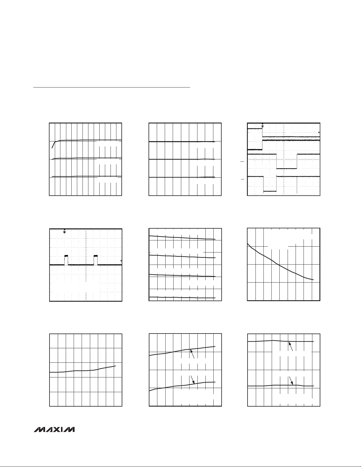
WETTING CURRENT vs. VS VOLTAGE
MAX13362 toc01
VS VOLTAGE (V)
WETTING CURRENT (mA)
13 161514 17
5
10
15
20
0
5187109811612
I
WETT
= 15mA
I
WETT
= 10mA
I
WETT
= 5mA
WETTING CURRENT vs. TEMPERATURE
MAX13362 toc02
TEMPERATURE (°C)
WETTING CURRENT (mA)
400
5
10
15
20
0
-40 8020-20 120 14010060
I
WETT
= 15mA
I
WETT
= 10mA
I
WETT
= 5mA
VS SUPPLY CURRENT vs. TEMPERATURE
(CONTINUOUS MODE)
MAX13362 toc05
TEMPERATURE (°C)
SUPPLY CURRENT (μA)
1000
1400
2200
600
1800
2600
200
I
WETT
= 15mA FOR ALL CHANNELS
I
WETT
= 10mA FOR ALL CHANNELS
I
WETT
= 5mA FOR ALL CHANNELS
ALL CHANNELS OPEN
I
WETT
= 0mA FOR ALL CHANNELS
400-40 8020-20 120 14010060
VS SUPPLY CURRENT vs. TEMPERATURE
(POLLING MODE)
MAX13362 toc06
TEMPERATURE (°C)
SUPPLY CURRENT (μA)
20 12040 10060-20
100
110
120
130
90
-40 140080
POLLING TIME = 65.536ms
POLLING ACTIVE TIME = 1.024ms
ALL CHANNELS OPEN
I
WETT
= 5mA
VS SUPPLY CURRENT vs. TEMPERATURE
(SHUTDOWN MODE)
MAX13362 toc07
TEMPERATURE (°C)
SUPPLY CURRENT (μA)
600
5.6
5.3
5.9
6.2
6.5
5.0
-40 -20 20 8040 140100 120
Typical Operating Characteristics
(V
DD
= VSD= 5V, VVS= 14V, TA= +25°C, unless otherwise noted.)
WETTING CURRENT
(POLLING MODE)
5mA
MAX13362 toc04
SWITCH STATUS CHANGE
I
WETT
(CONTINUOUS MODE)
V
10V
IN0
0mA
V
INT
V
CS
5mA
10ms/div
MAX13362 toc03
0V
10V/div
5mA/div
2V/div
2V/div
4.096ms POLLING TIME
WETTING CURRENT (5mA/div)
512μs POLLING ACTIVE TIME
1ms/div
SWITCH THRESHOLD vs. TEMPERATURE
(HIGH SIDE SWITCH)
3.4
3.3
SWITCH OPEN TO CLOSE
3.2
SWITCH THRESHOLD (V)
3.1
3.0
-40 140080
SWITCH CLOSE TO OPEN
HIGH SIDE SWITCH
15mA WETTING CURRENT
100Ω INCLUDED
20 12040 10060-20
TEMPERATURE (°C)
MAX13362 toc08
SWITCH THRESHOLD vs. TEMPERATURE
(LOW-SIDE SWITCH)
3.4
3.3
3.2
SWITCH THRESHOLD (V)
3.1
3.0
-40 140080
SWITCH OPEN TO CLOSE
SWITCH CLOSE TO OPEN
LOW-SIDE SWITCH
15mA WETTING CURRENT
20 12040 10060-20
TEMPERATURE (°C)
MAX13362 toc09
Page 6

MAX13362
24-Channel Automotive Switch Monitor
6 _______________________________________________________________________________________
Pin Description
Typical Operating Characteristics (continued)
(V
DD
= VSD= 5V, VVS= 14V, TA= +25°C, unless otherwise noted.)
PIN NAME FUNCTION
1, 2, 11,
29, 30
N.C. No Connection. Not internally connected.
3 IN17 Switch Monitor Input Channel 17. Connect IN17 to a ground-connected switch.
4 IN18 Switch Monitor Input Channel 18. Connect IN18 to a ground-connected switch.
5 IN19 Switch Monitor Input Channel 19. Connect IN19 to a ground-connected switch.
6 IN20 Switch Monitor Input Channel 20. Connect IN20 to a ground-connected switch.
7 IN21 Switch Monitor Input Channel 21. Connect IN21 to a ground-connected switch.
8 IN22 Switch Monitor Input Channel 22. Connect IN22 to a ground-connected switch.
9IN23
Switch Monitor Input Channel 23. Connect IN23 to a battery-connected or ground-connected switch.
When used for a battery-connected switch, add a 100Ω series protection resistor to the input.
10 INT
Inter r up t Outp ut. INT i s an op en- d r ai n outp ut that asser ts l ow w hen one or m or e of the i np uts ( IN 0–IN 23)
chang e state and ar e enab l ed for i nter r up ts, or w hen the over tem p er atur e thr eshol d i s exceed ed .
12 CLK SPI Serial Clock Input
13 SDO
SPI Serial Data Output. SPI data is output on SDO on the rising edges of CLK while CS is held low.
SDO is high impedance when CS is high. Connect SDO to a microcontroller data input or to a
succeeding device in a daisy chain.
14 CS
SPI Chip-Select Input. Drive CS low to enable clocking of data into and out of the IC. SPI data is
latched into the device on the rising edge of CS.
15 SDI
SPI Serial Data Input. SPI data is latched into the internal shift register on the falling edges of CLK
while CS is held low. SDI has an internal 50kΩ pulldown resistor. Connect SDI to the SDO of a
preceding device in a daisy chain or to the microcontroller data output.
16, 18 GND Ground. Pins 16 and 18 must be connected to ground.
17 V
DD
Logic Supply Voltage. Connect VDD to a 3.3V or 5V logic supply. Bypass VDD to GND with at least a
0.1µF capacitor placed as close as possible to V
DD
.
SWITCH THRESHOLD vs. VS VOLTAGE
(LOW-SIDE SWITCH)
3.5
SWITCH STATUS CHANGE
(POLLING MODE)
MAX13362 toc11
3.4
3.3
SWITCH OPEN TO CLOSE
MAX13362 toc10
V
IN
3.2
SWITCH THRESHOLD (V)
3.1
3.0
91811 15
SWITCH CLOSE TO OPEN
12 1713 161410
VS VOLTAGE (V)
V
INT
10V
5V/div
0V
2V/div
0V
2ms/div
Page 7

MAX13362
24-Channel Automotive Switch Monitor
_______________________________________________________________________________________ 7
Pin Description (continued)
PIN NAME FUNCTION
19, 20 VS
Supply Voltage Input. VS should be protected from reverse battery using a series diode. Bypass VS to
GND with a 0.1µF ceramic capacitor placed as close as possible to VS. In addition, bypass VS with a
47µF or greater capacitor.
21 SD
Shutdown Input. Drive SD low to place the IC into shutdown mode. Drive SD high for normal operation.
SD is battery-voltage compatible.
22 IN0
Switch Monitor Input Channel 0. Connect IN0 to a battery-connected or ground-connected switch.
When used for a battery-connected switch, add a 100Ω series protection resistor to the input.
23 IN1
Switch Monitor Input Channel 1. Connect IN1 to a battery-connected or ground-connected switch.
When used for a battery-connected switch, add a 100Ω series protection resistor to the input.
24 IN2
Switch Monitor Input Channel 2. Connect IN2 to a battery-connected or ground-connected switch.
When used for a battery-connected switch, add a 100Ω series protection resistor to the input.
25 IN3
Switch Monitor Input Channel 3. Connect IN3 to a battery-connected or ground-connected switch.
When used for a battery-connected switch, add a 100Ω series protection resistor to the input.
26 IN4 Switch Monitor Input Channel 4. Connect IN4 to a ground-connected switch.
27 IN5 Switch Monitor Input Channel 5. Connect IN5 to a ground-connected switch.
28 IN6 Switch Monitor Input Channel 6. Connect IN6 to a ground-connected switch.
31 IN7 Switch Monitor Input Channel 7. Connect IN7 to a ground-connected switch.
32 IN8 Switch Monitor Input Channel 8. Connect IN8 to a ground-connected switch.
33 IN9 Switch Monitor Input Channel 9. Connect IN9 to a ground-connected switch.
34 IN10 Switch Monitor Input Channel 10. Connect IN10 to a ground-connected switch.
35 IN11 Switch Monitor Input Channel 11. Connect IN11 to a ground-connected switch.
36 IN12 Switch Monitor Input Channel 12. Connect IN12 to a ground-connected switch.
37 IN13 Switch Monitor Input Channel 13. Connect IN13 to a ground-connected switch.
38 IN14 Switch Monitor Input Channel 14. Connect IN14 to a ground-connected switch.
39 IN15 Switch Monitor Input Channel 15. Connect IN15 to a ground-connected switch.
40 IN16 Switch Monitor Input Channel 16. Connect IN16 to a ground-connected switch.
— EP Exposed Pad. Connect EP to GND for enhanced thermal performance.
Page 8

MAX13362
24-Channel Automotive Switch Monitor
8 _______________________________________________________________________________________
Functional Diagram
VS V
DD
IN10
IN11
IN12
IN13
IN14
IN15
IN16
IN17
IN18
IN19
IN20
IN21
IN22
IN23
IN0
IN1
IN2
IN3
IN4
IN5
IN6
IN7
IN8
IN9
MAX13362
WETTING
CURRENT
CONTROL
1 OF 24
24 OF 24
REF
GENERATOR
SHIFT
REGISTER
+
CONTROL
SDO
CS
CLK
INT
SD
SDI
GND
Page 9

Detailed Description
The MAX13362 is a 24-channel automotive contact
monitor designed as an interface between mechanical
switches and low-voltage microcontrollers or other logic
circuits. It features an SPI interface to monitor individual
switch inputs and to configure interrupt capability, wetting current, switch configuration (battery-connected or
ground-connected), polling time and polling active
time. Any switch status change will cause an interrupt
signal if the switch is interrupt enabled. The MAX13362
has three modes of operation: continuous mode, polling
mode, and shutdown mode.
VDDand VS
VDDis the power-supply input for the logic input/
output circuitry. Connect VDDto a 3V to 5.5V logic-level
supply. Bypass VDDto GND with at least a 0.1µF
capacitor placed as close as possible to VDD.
VS is the main power-supply input. Bypass VS to GND
with a 0.1µF ceramic capacitor placed as close as possible to VS. In addition, bypass VS with a 47µF or
greater capacitor.
Mechanical Switch Inputs (IN0–IN23)
IN0–IN23 are the inputs for remote mechanical switches. The switch status is indicated by the S0–S23 bits in
the status register, and each switch input can be programmed to assert an interrupt (INT) by writing to the
IE0–IE23 bits in the command register. All switch inputs
are interrupt disabled upon power-up.
The IN4–IN22 inputs are intended for ground-connected switches. The IN0–IN3 and IN23 inputs can be programmed for either ground-connected switches or
battery-connected switches by writing to the LH0–LH3
and LH23 bits (see Table 2). The default configuration
of the IN0–IN3 and IN23 inputs after power-up is for
ground-connected switches.
Wetting Current
The MAX13362 applies a programmable wetting current
to any closed switch to clean switch contacts that are
exposed to adverse conditions. The wetting current for
each switch can be set to 0mA, 5mA, 10mA, or 15mA
by the W_.0 and W_.1 data bits in the command registers (see Table 5) by means of an SPI data transaction.
When using wetting current, special care must be
taken to avoid exceeding the maximum power dissipation of the MAX13362 (see the
Applications Information
section). Disabling the wetting current or limiting the
active-wetting current time reduces power consumption. The default state upon power-up is with wetting
current disabled.
Interrupt Output (
INT
)
INT is an active-low, open-drain output that asserts low
when any of the switch inputs change state and is
enabled for interrupts, or when the overtemperature
threshold is exceeded. An external pullup resistor to
VDDis needed on INT. INT is cleared when CS is driven
low for a read/write operation. However, in polling mode,
any switch state change or overtemperature change
which occurs during an SPI transaction is stored and
causes an additional interrupt after the SPI transaction is
over and CS goes high (shown in Figure 2).
If VDDis absent, the INT output is functional provided
that it is pulled up to a different supply voltage.
MAX13362
24-Channel Automotive Switch Monitor
_______________________________________________________________________________________ 9
Figure 2. Switch State Change During the SPI transaction
CS
CLK
INT
SWITCH STATUS CHANGE
NEW INTERRUPT
Page 10

MAX13362
Serial Peripheral Interface
(
CS
, SDO, SDI, CLK)
The MAX13362 operates as a serial peripheral interface
(SPI) slave device. An SPI master accesses and programs the MAX13362 by reading/writing the control
registers. The control registers are 32 bits wide, have 2
command bits (or register addresses) and 30 data bits
(see Table 1). Figure 3 shows the read/write sequence
through SPI. The SPI logic counts the number of bits
clocked into the IC (using a modulo-32 counter so that
daisy chaining is possible) and enables data latching
only if exactly 32 bits (or an integer multiple thereof)
have been clocked in.
Status Register
The status register contains the status of the switches
connected to IN0–IN23. The status register also contains an overtemperature warning bit, a power-on-reset
bit and a device type bit (see Table 1). The status register is accessed by the SPI-compatible interface.
24-Channel Automotive Switch Monitor
10 ______________________________________________________________________________________
Figure 3. SPI Read/Write Sequence
BIT NAME BIT DESCRIPTION
CB0, CB1 Command bits. Select the internal register to which data bits D0–D29 are to be written.
D0–D29 Data bits.
S0–S23 Switch state bit. 0 = switch open, 1 = switch closed.
T Overtemperature bit. When overtemperature occurs, this bit is set to 1. It is reset on the rising edge of CS.
RST
Power-on-reset bit. It indicates whether the IC has had a power-on-reset since the last SPI read. 0 = device has
been reset. RST is set to 1 on the rising edge of CS.
DT Device type. 0 = reserved for future use, 1 = MAX13362.
Table 1. Bit Description
CS
CLK
SDI
SDO
RSTDTZ
NOTE: X = UNUSED, Z = HIGH IMPEDANCE.
D1 D2 D3 D4 D5 D6 D7 D8 D9 D10 D11
T S0 S8S7S6S5S4S3S2S1 S9 S10
D12CB0 CB1 D0
S19
S20 S21 S22 S23 x x xx x
D24D13 D14 D15 D16 D17 D18 D19 D20 D21 D22 D23 D29D25 D26 D27 D28
ZS11 S12 S13 S14 S15 S16 S17 S18
Page 11

Command Register
Three 32-bit command registers are used to configure
the MAX13362 for various modes of operation and are
accessed by the SPI-compatible interface (see Table 2).
LH_: Switch Configuration for IN0–IN3 and IN23
The LH0–LH3 and LH23 bits set the switch configuration
for IN0–IN3 and IN23, respectively. Set LH_ to 0 to configure the input channel to ground connected. Set LH_
to1 to configure the input channel to battery connected.
The default configuration after power-on is LH_ = 0,
ground connected.
P0–P3: Polling Time
P0–P3 are used to set the polling time as shown in Table 3.
PA0–PA2: Polling Active Time
PA0–PA2 are used to set the polling active time as
shown in Table 4.
MAX13362
24-Channel Automotive Switch Monitor
______________________________________________________________________________________ 11
P3
POLLING TIME (ms)
0 0 0 0 Continuous*
0001 4.096
0010 4.096
0011 4.096
0100 4.096
0101 4.096
0110 8.192
0 1 1 1 16.384
1 0 0 0 32.768
1 0 0 1 65.536
1010 131
1011 262.1
1100 524.3
1 1 0 1 1049
1 1 1 0 2097
1 1 1 1 4194
Table 3. Polling Time Setting
D29
X
W23.0W22.0W21.0W20.0W19.0W18.0W17.0W16.0W15.0W14.0W13.0W12.0W11.0W10.0W9.0W8.0W7.0W6.0W5.0W4.0W3.0W2.0W1.0W0.
X
W23.1W22.1W21.1W20.1W19.1W18.1W17.1W16.1W15.1W14.1W13.1W12.1W11.1W10.1W9.1W8.1W7.1W6.1W5.1W4.1W3.1W2.1W1.1W0.
LH2
3
NO OPERATION (NO DATA WRITTEN)
Table 2. Command Register Map
*
Default POR Value.
*
Default POR value.
Table 4. Polling-Active Time Setting
PA2
POLLING ACTIVE TIME (µs)
000 64
001 128
010 256
0 1 1 512*
1 0 0 1024
1 0 1 2048
1 1 0 4096
1 1 1 4096
D28 D27 D26 D25 D24 D23 D22 D21 D20 D19 D18 D17 D16 D15 D14 D13 D12 D11 D10 D9 D8 D7 D6 D5 D4 D3 D2 D1 D0 CB1 CB0
PA2 PA1 PA0
LP
P3 P2 P1 P0
LH3 LH2 LH1 LH0 IE23 IE22 IE21 IE20 IE19 IE18 IE17 IE16 IE15 IE14 IE13 IE12 IE11 IE10 IE9 IE8 IE7 IE6 IE5 IE4 IE3 IE2 IE1 IE0 X 1 0
P2 P1 P0
PA1 PA0
0
1
X00
X01
11
Page 12

MAX13362
IE_: Interrupt Enable
The IE_ bit programs the switch input channel, IN_, to
be interrupt-enabled or interrupt-disabled (0 = interrupt
disabled, 1 = interrupt enabled). The default value after
power-on is 0.
W_.0 and W_.1: Wetting Current
W_.0 and W_.1 bits set the corresponding switch
channel-wetting current as shown in Table 5.
LP: Low Quiescent Current Bit
In polling mode, when LP is set to 0, the IC is operating
with the lowest quiescent current. The channels that are
not enabled to interrupt have their wetting current disabled and are not monitored. The first pulse of wetting
current after the switch is closed and sampled is 5mA
unless the wetting current for that channel is set to
0mA. The default value of LP after power-on is 0. When
LP is 1, all channels are monitored and the wetting current for each channel is set to the value determined by
W_.0 and W_.1. If the MAX13362 is in continuous
mode, LP is ignored.
Operating Modes
The MAX13362 features three modes of operation: continuous mode, polling mode, and shutdown mode. In
continuous mode, the wetting currents (if enabled) are
continuously applied to the closed switches. In polling
mode, the wetting currents are applied to the closed
switches for a preset duration to reduce the power consumption. In shutdown mode, all switch inputs are high
impedance and all circuitry is shutdown.
Continuous Mode Operation (P0–P3 = 0)
In continuous mode, reading of the switch status is initiated by a falling edge on CS. The microcontroller initiates a low pulse on CS to update the MAX13362 switch
status register. If INT remains high, no action needs be
taken by the microcontroller. If INT goes low, the micro-
controller may perform a read operation to read the
updated switch status. On the rising edge of CS, INT is
updated. To get correct data, the microcontroller must
wait 10µs before initiating a switch status read operation. (See Figure 4.)
Polling-Mode Operation
In polling mode (see Figure 5), each switch input is
sampled for a programmable polling active time set by
the PA0–PA2 bits between 64µs and 4ms (see Table 4).
Sampling is repeated at a period set by the P0–P3 bits
(from 4ms to continuous, see Table 3). All switch inputs
are sampled simultaneously at the end of the polling
active time. Wetting currents (if enabled) are applied to
closed switches during the polling active time.
Therefore, the polling mode reduces the current consumption from the VS power supply to some value
dependent on the polling time chosen.
24-Channel Automotive Switch Monitor
12 ______________________________________________________________________________________
*
Default POR value.
Table 5. Wetting Current Setting
W_.1 W_.0 WETTING CURRENT (mA)
00 0*
01 5
10 10
11 15
Figure 4. Continuous Mode Operation
Figure 5. Switch Sampling in Polling Mode
CS
SWITCH
STATUS
CHANGE
INT
INT UPDATED, PERFORM READ OPERATION
GROUND-CONNECTED
SWITCH-INPUT
INT
POLLING
ACTIVE TIME
POLLING TIME
SWITCH
POSITION
SAMPLED
SWITCH OPEN
POLLING ACTIVE TIME
SWITCH
POSITION
SAMPLED
Page 13

Any switch position change (if the switch is interruptenabled) is signaled through the active-low open-drain
INT output. The INT output is cleared when CS goes
low.
Shutdown Mode
In shutdown mode, all switch inputs are high impedance and the external switches are no longer monitored, reducing current consumption on VS to 6µA
(typ). The IC resets upon entering shutdown mode and
the contents of the command registers are lost.
Therefore, any setting other than power-on-reset
defaults needs to be reprogrammed after exiting from
the shutdown mode.
Applications Information
Overtemperature Protection
If the IC junction temperature exceeds +165°C, an
interrupt signal is generated and the wetting currents
are disabled to reduce the on-chip power dissipation.
During an overtemperature event, the last switch status
is retained in internal memory and the switch status is
not updated. The interrupt output is cleared when CS
goes high, but the overtemperature bit T in the output
word remains for as long as the overtemperature condition persists. When the junction temperature drops by
15°C, the wetting currents are re-enabled and there is a
1ms blanking time before the switches can be polled.
Reverse-Battery Tolerance
The IN0–IN23 switch inputs withstand up to -15V DC
voltage without damage. A reverse-battery diode is
needed to protect VS as shown in the
Typical
Application Circuit
. SD can be controlled from a bat-
tery-level source but should be protected against
reverse battery in the application.
Wetting Current and Power Dissipation
The maximum power dissipation happens when all
switch inputs configured with 15mA continuous wetting
current are all closed. Assuming the battery voltage is
14V, the corresponding power dissipated by the IC is
24 x 14V x 15mA = 5040mW. This exceeds the
absolute maximum power dissipation of 2963mW. In
polling mode, the wetting currents are pulsed at the
programmed polling time to reduce the total power dissipated in the IC.
ISO 7637 Pulse Immunity
VS, SD, and IN0–IN23 are potentially exposed to ISO
7637 pulses. Bypass VS with a 0.1µF and a 47µF
capacitor. The VS and SD voltage must be limited
below 40V during load dump. Bypass IN0–IN23 with at
least 0.047µF capacitors at the ECU connector. When
IN0–IN3 or IN23 inputs are used with battery-connected
switches, a 100Ω series resistor is needed. These
external components allow VS, SD, and IN0–IN23 to
withstand ISO 7637 pulses in the application circuit.
Mechanical Switch Characteristics
The MAX13362 is designed to operate with switches
that have the following characteristics:
1) Minimum resistance value with switch open (due to
leakage): 10kΩ.
2) Maximum resistance value with switch closed:
100Ω.
Chip Information
PROCESS: BiCMOS
MAX13362
24-Channel Automotive Switch Monitor
______________________________________________________________________________________ 13
Page 14

MAX13362
24-Channel Automotive Switch Monitor
Maxim cannot assume responsibility for use of any circuitry other than circuitry entirely embodied in a Maxim product. No circuit patent licenses are
implied. Maxim reserves the right to change the circuitry and specifications without notice at any time.
14
____________________Maxim Integrated Products, 120 San Gabriel Drive, Sunnyvale, CA 94086 408-737-7600
© 2009 Maxim Integrated Products Maxim is a registered trademark of Maxim Integrated Products, Inc.
PACKAGE TYPE PACKAGE CODE DOCUMENT NO.
40 TQFN-EP T4066+5
21-0141
Package Information
For the latest package outline information and land patterns, go to www.maxim-ic.com/packages.
 Loading...