

Page 1
General Description
The MAX13330/MAX13331 stereo headphone amplifiers
are designed for automotive applications requiring output short-circuit and ESD protection to battery/ground
with diagnostics. These devices use Maxim’s unique,
patented†DirectDrive®architecture to produce a
ground-referenced output from a single supply, eliminating the need for large DC-blocking capacitors, saving board space and component height. The gain of the
amplifier is set internally (-1.5V/V) on the MAX13330 or
adjusted externally with resistors on the MAX13331.
The MAX13330/MAX13331 deliver 120mW per channel
into a 16Ω load or 135mW into a 32Ω load and have a
low 0.01% THD+N. Low output impedance and the efficient integrated charge pump allows the device to drive
loads as low as 8Ω, enabling the use of small loudspeakers. An 80dB at 217Hz PSRR allows these
devices to operate from noisy digital supplies without
an additional linear regulator. These devices include
±15kV Human Body Model ESD protection and shortcircuit protection up to +45V at the headphone outputs.
Comprehensive click-and-pop circuitry suppresses
audible clicks and pops on startup and shutdown. A
low-power shutdown mode reduces the supply current
to 3µA (typ).
The MAX13330/MAX13331 are specified from -40°C to
+105°C AEC-Q100 Level 2 automotive temperature
range and are available in a 16-pin QSOP package.
Applications
Automotive Entertainment Systems
Automotive Rear Seat Entertainment Systems
Features
♦ 4V to 5.5V Single-Supply Operation
♦ 2MHz Charge Pump Prevents AM Radio
Interference
♦ Ground-Referenced Outputs Eliminate Bulky DC-
Blocking Capacitors
♦ Short-to-Ground and Battery (V
BAT
up to +45V)
Output Protection, Load Dump Protection
♦ Short-Circuit Diagnostic Output
♦ Adjustable Gain (MAX13331) or Fixed -1.5V/V Gain
(MAX13330)
♦ 135mW per Channel into 32Ω at 1% THD+N
♦ Low 0.01% THD+N
♦ Integrated Click-and-Pop Suppression
♦ High PSRR Eliminates LDO
♦ No Degradation of Low-Frequency Response Due
to Output Capacitors
♦ ±15kV Human Body Model ESD Protection for
Output Pins
MAX13330/MAX13331
Automotive DirectDrive Headphone Amplifiers
with Output Protection and Diagnostics
________________________________________________________________
Maxim Integrated Products
1
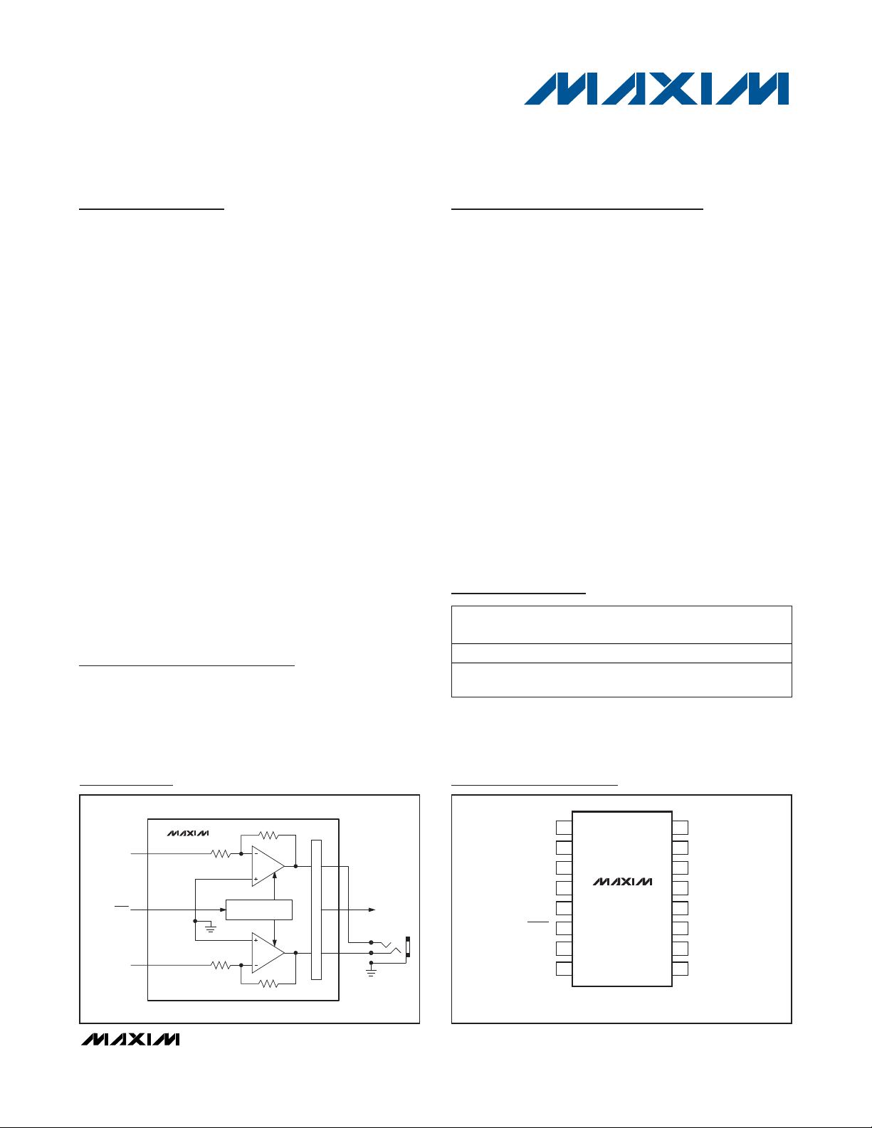
Pin Configuration
Simplified Block Diagram
19-4341; Rev 0; 10/08
For pricing, delivery, and ordering information, please contact Maxim Direct at 1-888-629-4642,
or visit Maxim’s website at www.maxim-ic.com.
DirectDrive is a registered trademark of Maxim Integrated
Products, Inc.
†
U.S. Patent #7,061,327
Ordering Information
+
Denotes a lead-free/RoHS-compliant package.
T = Tape-and-reel.
/V denotes an automotive qualified part.
Typical Application Circuits appear at end of data sheet.
PART
TEMP
RANGE
PIN-
PACKAGE
M A X1 3 3 3 0 GE E /V + T
16 QSOP
M A X1 3 3 3 1 GE E /V + T
E xter nal l y
Set
16 QSOP
GAIN
-1.5V/V - 40°C to + 105°C
- 40°C to + 105°C
LEFT-CHANNEL
RIGHT-CHANNEL
AUDIO IN
SHDN
AUDIO IN
INL
MAX13330
CLICK-AND-POP
SUPPRESSION
OUTPUT PROTECTION & DIAGNOSTICS
DIAGNOSTICS
OUTPUT
SGND
INR
SGND
V
SHDN
CPVDD
C1P
1
2
3
4
DD
6
7
8
+
MAX13330
MAX13331
QSOP
16
15
14
13
125
11
10
9
OUTL
PGND
V
SS
OUTR
DIAG
CPVSS
C1N
PGND
Page 2
MAX13330/MAX13331
Automotive DirectDrive Headphone Amplifiers
with Output Protection and Diagnostics
2 _______________________________________________________________________________________
ABSOLUTE MAXIMUM RATINGS
ELECTRICAL CHARACTERISTICS
(VDD= V
CPVDD
= +5V, V
SGND
= V
PGND
= 0, SHDN = VDD, C1 = C2 = 1µF, RL= ∞, resistive load referenced to ground, for
MAX13330 gain = -1.5V/V (internally set), for MAX13331 gain = -1.5V/V (R
IN
= 30kΩ, RFB= 45kΩ), TA= TJ= -40°C to +105°C, unless
otherwise noted. Typical values are at T
A
= +25°C, unless otherwise noted.) (Note 2)
Stresses beyond those listed under “Absolute Maximum Ratings” may cause permanent damage to the device. These are stress ratings only, and functional
operation of the device at these or any other conditions beyond those indicated in the operational sections of the specifications is not implied. Exposure to
absolute maximum rating conditions for extended periods may affect device reliability.
Note 1: Package thermal resistances were obtained using the method described in JEDEC specification JESD51-7, using a four-
layer board. For detailed information on package thermal considerations, refer to http://www.maxim-ic.com/thermal-tutorial
.
V
DD
, CPVDD to SGND..............................................-0.3V to +6V
V
SS
, CPVSS to SGND ...............................................+0.3V to -6V
V
DD
, CPVDD ............................................................-0.3V to 0.3V
V
SS
, CPVSS..............................................................-0.3V to 0.3V
SHDN, DIAG to SGND................................-0.3V to (V
DD
+ 0.3V)
OUT_ to PGND.......................................(V
CPVSS
- 0.3V) to +45V
IN_ to SGND (MAX13330)................(V
SS
- 0.3V) to (VDD+ 0.3V)
IN_ to SGND (MAX13331)..........................-0.3V to (V
DD
+ 0.3V)
C1P to PGND.........................................-0.3V to (V
CPVDD
+0.3V)
C1N to PGND.............................................(V
SS
- 0.3V) to + 0.3V
Output Short-Circuit Duration.....................................Continuous
Continuous Power Dissipation (T
A
= +70°C)
16-Pin QSOP (derate 8.3mW/°C above +70°C)) ......666.7mW
Junction-to-Case Thermal Resistance (θ
JC
) (Note 1)
θ
JC
............................................................................... 37°C/W
Junction-to-Ambient Thermal Resistance (θ
JA
) (Note 1)
θ
JA
............................................................................. 120°C/W
Operating Temperature Range .........................-40°C to +105°C
Junction Temperature......................................................+150°C
Storage Temperature Range .............................-65°C to +150°C
Lead Temperature (soldering, 10s) .................................+300°C
PARAMETER
CONDITIONS
UNITS
GENERAL
Amplifier Supply Voltage Range V
DD
4.0 5.5 V
Charge-Pump Supply Voltage
Range
4.0 5.5 V
Charge-Pump Output Voltage
V
Quiescent Supply Current I
DD
RL = ∞ 10 mA
Shutdown Supply Current I
SHDN
10 µA
SHDN Input-Logic High V
IH
2V
SHDN Input-Logic Low V
IL
0.8 V
SHDN Input Leakage Current -1 +1 µA
SHDN to Full Operation Time t
SON
µs
DIAGNOSTICS
No fault
0.02 x
OUTR short to
SGND
0.22 x
0.25 x
0.28 x
OUTL short to
SGND
0.47 x
0.50 x
0.53 x
OUTR short to
V
BAT
0.72 x
0.75 x
0.78 x
Diagnostic Output Voltage V
DIAG
R
DIAG
= ∞,
T
A
= +25°C
OUTL short to
V
BAT
0.97 x
V
Short-to-SGND Threshold
mA
Short-to-V
BAT
Threshold
mA
SYMBOL
MIN TYP MAX
V
CPVDD
V
CPVSS
-V
DD
100
V
DD
V
DD
V
DD
V
DD
V
DD
V
DD
130
130
V
DD
V
DD
V
DD
V
DD
V
DD
Page 3
MAX13330/MAX13331
Automotive DirectDrive Headphone Amplifiers
with Output Protection and Diagnostics
_______________________________________________________________________________________ 3
ELECTRICAL CHARACTERISTICS (continued)
(VDD= V
CPVDD
= +5V, V
SGND
= V
PGND
= 0, SHDN = VDD, C1 = C2 = 1µF, RL= ∞, resistive load referenced to ground, for
MAX13330 gain = -1.5V/V (internally set), for MAX13331 gain = -1.5V/V (R
IN
= 30kΩ, RFB= 45kΩ), TA= TJ= -40°C to +105°C, unless
otherwise noted. Typical values are at T
A
= +25°C, unless otherwise noted.) (Note 2)
PARAMETER
CONDITIONS
UNITS
AMPLIFIERS
Voltage Gain A
V
MAX13330
V/V
Gain Matching MAX13330
%
Input Offset Voltage ±1 ±6 mV
Input Bias Current V
IN_
= 0 50 nA
Input Impedance R
IN
MAX13330 20 30 kΩ
DC, V
DD
= 4.0V to 5.5V, input referred -86 dB
Power-Supply Rejection Ratio PSRR
f =1kHz, V
RIPPLE
= 100mV
P-P
-80 dB
RL = 8Ω 75
RL = 16Ω
Output Power Per Channel P
OUT_
THD+N = 1%;
V
DD
= V
CPVDD
= 5V;
f
IN
= 1kHz
R
L
= 32Ω
mW
Output Voltage V
OUT_
RL = 1kΩ 2
V
RMS
Output Impedance in Shutdown 14 kΩ
RL = 16Ω, P
OUT
= 100mW, f = 1kHz
%
Total Harmonic Distortion Plus
Noise
RL = 32Ω, P
OUT
= 125mW, f = 1kHz
%
Signal-to-Noise Ratio SNR
dB
Noise V
n
f = 22Hz to 22kHz bandwidth; inputs
AC-coupled to grounded
6
µV
RMS
Slew Rate SR 0.3 V/µs
Maximum Capacitive Load C
L
No sustained oscillation
pF
Into shutdown -80
Click-and-Pop Level K
CP
Peak voltage, TA =
+25°C, A-weighted,
32 samples per
second; Inputs ACcoupled to ground
Out of shutdown -60
V
Charge-Pump Oscillator
Frequency
f
OSC
1.9 2.2 2.5 MHz
Crosstalk RL = 32Ω, VIN = 200mV
P-P
, f = 10kHz -75 dB
Thermal-Shutdown Temperature
°C
Thermal-Shutdown Hysteresis 10 °C
ESD Protection Human Body Model (OUTR and OUTL)
kV
Note 2: All devices are 100% tested at TA= +25°C; specifications over temperature limits are guaranteed by design and QA
sampling.
SYMBOL
THD+N
RL = 32Ω , P
= 135m W , f = 22H z to 22kH z 100
OU T
MIN TYP MAX
-1.48 -1.5 -1.52
±0.2
120
135
0.03
0.01
+155
±15
3000
Page 4
MAX13330/MAX13331
Automotive DirectDrive Headphone Amplifiers
with Output Protection and Diagnostics
4 _______________________________________________________________________________________
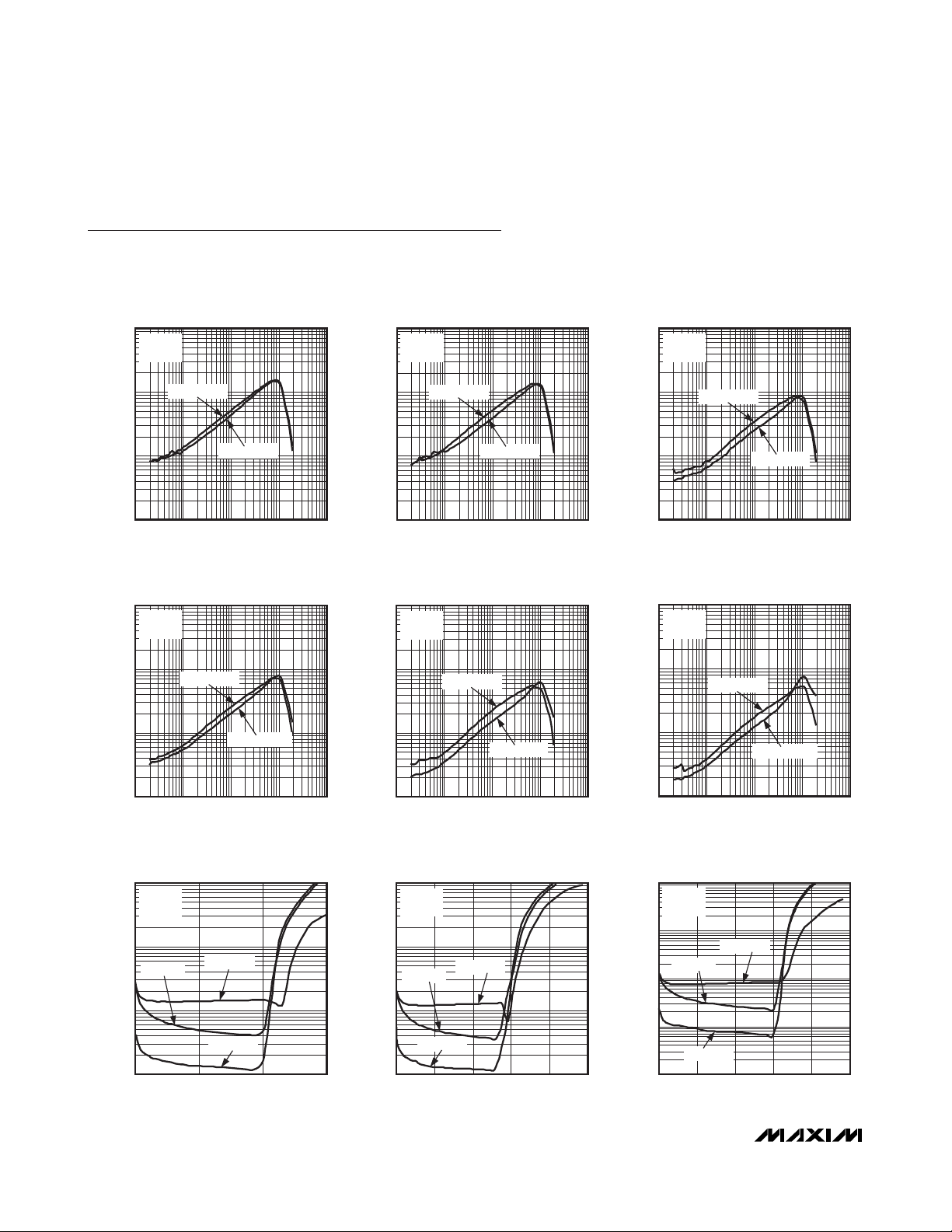
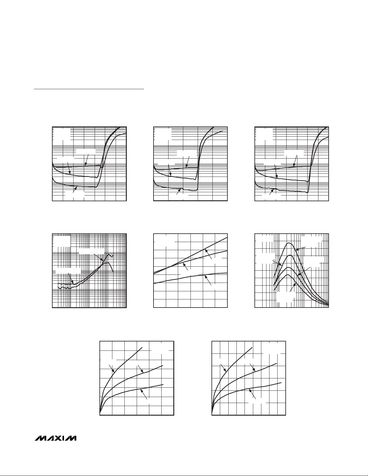
Typical Operating Characteristics
(VDD= V
CPVDD
= 5V, V
SGND
= V
PGND
= 0, C1 = C2 = 1µF, RL= ∞, gain = -1.5V/V, THD+N measurement bandwidth = 22Hz to 22kHz,
T
A
= +25°C, unless otherwise noted.)
1
0.1
TOTAL HARMONIC DISTORTION
PLUS NOISE vs. FREQUENCY
VDD = 4V
= 8Ω
R
L
P
= 25mW
OUT
TOTAL HARMONIC DISTORTION
PLUS NOISE vs. FREQUENCY
1
VDD = 4V
= 16Ω
R
L
0.1
P
OUT
= 25mW
MAX13330/31 toc01
TOTAL HARMONIC DISTORTION
PLUS NOISE vs. FREQUENCY
1
VDD = 5V
= 8Ω
R
L
P
0.1
OUT
= 25mW
MAX13330/31 toc02
MAX13330/31 toc03
THD+N (%)
0.01
0.001
0.01 100
THD+N (%)
0.001
TOTAL HARMONIC DISTORTION
PLUS NOISE vs. FREQUENCY
1
VDD = 5V
= 16Ω
R
L
0.1
0.01
0.01 100
P
= 45mW
OUT
0.1 1 10
FREQUENCY (kHz)
P
= 50mW
OUT
P
= 100mW
OUT
0.1 1 10
FREQUENCY (kHz)
THD+N (%)
0.001
MAX13330/31 toc04
THD+N (%)
0.001
0.01
0.01 100
1
VDD = 4V
R
0.1
0.01
0.01 100
TOTAL HARMONIC DISTORTION
PLUS NOISE vs. OUTPUT POWER
10
VDD = 4V
= 8Ω
R
L
1
fIN = 1kHz
THD+N (%)
0.1
0.01
0 75
fIN = 10kHz
fIN = 100Hz
5025
OUTPUT POWER (mW)
MAX13330/31 toc07
THD+N (%)
10
VDD = 5V
R
1
fIN = 1kHz
0.1
0.01
0 125
P
= 60mW
OUT
0.1 1 10
FREQUENCY (kHz)
TOTAL HARMONIC DISTORTION
PLUS NOISE vs. FREQUENCY
= 32Ω
L
P
= 25mW
OUT
P
= 70mW
OUT
0.1 1 10
FREQUENCY (kHz)
TOTAL HARMONIC DISTORTION
PLUS NOISE vs. OUTPUT POWER
= 8Ω
L
fIN = 10kHz
fIN = 100Hz
50 10025 75
OUTPUT POWER (mW)
THD+N (%)
0.001
MAX13330/31 toc05
THD+N (%)
0.001
MAX13330/31 toc08
THD+N (%)
0.001
0.01
0.01 100
0.1 1 10
P
= 75mW
OUT
FREQUENCY (kHz)
TOTAL HARMONIC DISTORTION
PLUS NOISE vs. FREQUENCY
1
VDD = 5V
= 32Ω
R
L
0.1
P
= 50mW
OUT
0.01
P
= 125mW
OUT
0.01 100
0.1 1 10
FREQUENCY (kHz)
TOTAL HARMONIC DISTORTION
PLUS NOISE vs. OUTPUT POWER
10
VDD = 4V
= 16Ω
R
L
1
fIN = 1kHz
0.1
0.01
0 125
fIN = 10kHz
fIN = 100Hz
50 10025 75
OUTPUT POWER (mW)
MAX13330/31 toc06
MAX13330/31 toc09
Page 5
MAX13330/MAX13331
Automotive DirectDrive Headphone Amplifiers
with Output Protection and Diagnostics
_______________________________________________________________________________________ 5
Typical Operating Characteristics (continued)
(VDD= V
CPVDD
= 5V, V
SGND
= V
PGND
= 0, C1 = C2 = 1µF, RL= ∞, gain = -1.5V/V, THD+N measurement bandwidth = 22Hz to 22kHz,
T
A
= +25°C, unless otherwise noted.)
TOTAL HARMONIC DISTORTION
PLUS NOISE vs. OUTPUT POWER
10
VDD = 5V
= 16Ω
R
L
1
fIN = 10kHz
fIN = 1kHz
0.1
THD+N (%)
0.01
fIN = 100Hz
0.001
0 10075 175
OUTPUT POWER (mW)
TOTAL HARMONIC DISTORTION
PLUS NOISE vs. FREQUENCY
1
VDD = 5V
= 1kΩ
R
L
V
= 2V
OUT_
0.1
V
0.01
THD+N (%)
0.001
0.0001
= 1V
OUT_
RMS
0.01 100
0.1 1 10
FREQUENCY (kHz)
RMS
TOTAL HARMONIC DISTORTION
PLUS NOISE vs. OUTPUT POWER
10
VDD = 4V
= 32Ω
R
L
MAX13330/31 toc10
12550 15025
1
fIN = 10kHz
fIN = 1kHz
0.1
THD+N (%)
0.01
0.001
fIN = 100Hz
0 125
50 10025 75
OUTPUT POWER (mW)
MAX13330/31 toc11
THD+N (%)
0.001
OUTPUT POWER vs. SUPPLY VOLTAGE
180
fIN = 1kHz
160
1% THD+N
140
MAX13330/31 toc13
120
100
80
60
OUTPUT POWER (mW)
40
20
RL = 32Ω
RL = 16Ω
RL = 8Ω
0
4.00 5.50
SUPPLY VOLTAGE (V)
5.254.754.50 5.004.25
MAX13330/31 toc14
OUTPUT POWER (mW)
TOTAL HARMONIC DISTORTION
PLUS NOISE vs. OUTPUT POWER
10
VDD = 5V
= 32Ω
R
L
1
fIN = 10kHz
0.1
0.01
fIN = 1kHz
fIN = 100Hz
0 10075 175
OUTPUT POWER (mW)
OUTPUT POWER vs. LOAD RESISTANCE
200
fIN = 1kHz
180
160
140
1% THD+N
= 5V
V
DD
120
100
80
60
40
20
0
0 1000
1% THD+N
= 4V
V
DD
10 100
LOAD RESISTANCE (Ω)
12550 15025
10% THD+N
= 5V
V
DD
10% THD+N
= 4V
V
DD
MAX13330/31 toc12
MAX13330/31 toc15
POWER DISSIPATION vs.
OUTPUT POWER PER CHANNEL
800
700
600
RL = 8Ω
500
400
300
POWER DISSIPATION (mW)
200
100
0
0 120
OUTPUT POWER PER CHANNEL (mW)
RL = 16Ω
RL = 32Ω
VDD = 4V
= 1kHz
f
IN
1006040 8020
1200
1000
MAX13330/31 toc16
800
600
400
POWER DISSIPATION (mW)
200
0
POWER DISSIPATION vs.
OUTPUT POWER PER CHANNEL
VDD = 5V
= 1kHz
f
IN
RL = 8Ω
0 180
OUTPUT POWER PER CHANNEL (mW)
RL = 16Ω
RL = 32Ω
80 14060 120 16020 10040
MAX13330/31 toc17
Page 6

MAX13330/MAX13331
Automotive DirectDrive Headphone Amplifiers
with Output Protection and Diagnostics
6 _______________________________________________________________________________________
Typical Operating Characteristics (continued)
(VDD= V
CPVDD
= 5V, V
SGND
= V
PGND
= 0, C1 = C2 = 1µF, RL= ∞, gain = -1.5V/V, THD+N measurement bandwidth = 22Hz to 22kHz,
T
A
= +25°C, unless otherwise noted.)
-40
-50
-60
-70
-80
PSRR (dB)
-90
-100
-110
-120
0.01 100
POWER-SUPPLY REJECTION RATIO
vs. FREQUENCY
VDD = 4V
VDD = 4V
OUTL
OUTR
VDD = 5V
OUTL
FREQUENCY (kHz)
VDD = 5V
OUTR
V
RIPPLE
RL = 32Ω
= 100mV
100.1 1
-40
CROSSTALK vs. FREQUENCY
VIN = 200mV
RL = 32Ω
-50
MAX13330/31 toc18
-60
-70
CROSSTALK (dB)
-80
P-P
-90
-100
0.01 100
P-P
RIGHT TO LEFT
LEFT TO RIGHT
0.1 1 10
FREQUENCY (kHz)
MAX13330/31 toc19
GAIN (dB)
GAIN FLATNESS vs. FREQUENCY
3.5
3.4
OUTR
3.3
3.2
3.1
MAX13330
= 100mV
V
IN
3.0
0.01 1000
OUTL
P-P
1000.1 101
FREQUENCY (kHz)
MAX13330/31 toc20
0
-20
-40
-60
-80
AMPLITUDE (dBV)
-100
-120
-140
05 20
SHUTDOWN CURRENT vs. TEMPERATURE
4.0
3.5
3.0
2.5
2.0
1.5
SHUTDOWN CURRENT (μA)
1.0
0.5
0
-50 5025 125
OUTPUT FFT
R
L
10 15
FREQUENCY (kHz)
075-25 100
TEMPERATURE (°C)
= 32Ω
10
9
MAX13330/31 toc21
8
7
6
5
4
3
SUPPLY CURRENT (mA)
2
1
0
SHUTDOWN CURRENT vs. SUPPLY VOLTAGE
5
MAX13330/31 toc24
4
3
2
SHUTDOWN CURRENT (μA)
1
0
SUPPLY CURRENT vs. SUPPLY VOLTAGE
4.00 4.25 5.50
4.00 5.25 5.50
SUPPLY VOLTAGE (V)
5.004.25 4.754.50
SUPPLY VOLTAGE (V)
SUPPLY CURRENT vs. TEMPERATURE
12
10
MAX13330/31 toc22
8
6
4
SUPPLY CURRENT (mA)
2
0
5.254.75 5.004.50
MAX13330/31 toc25
-50 5025 125
075-25 100
TEMPERATURE (°C)
EXITING SHUTDOWN TRANSIENT
200μs/div
MAX13330/31 toc26
MAX13330/31 toc23
SHDN
5V/div
OUTL
1V/div
OUTR
1V/div
Page 7

MAX13330/MAX13331
Automotive DirectDrive Headphone Amplifiers
with Output Protection and Diagnostics
_______________________________________________________________________________________ 7
Pin Description
Typical Operating Characteristics (continued)
(VDD= V
CPVDD
= 5V, V
SGND
= V
PGND
= 0, C1 = C2 = 1µF, RL= ∞, gain = -1.5V/V, THD+N measurement bandwidth = 22Hz to 22kHz,
T
A
= +25°C, unless otherwise noted.)
PIN NAME FUNCTION
1 INL Inverting Left-Channel Audio Input
2, 4 SGND
Amplifier Signal Ground. The noninverting inputs of the amplifiers are connected to the amplifier
signal ground. Connect both to the signal ground plane.
3 INR Inverting Right-Channel Audio Input
5V
DD
Amplifier Positive-Power Supply. Connect to positive supply. Bypass with a 1µF capacitor to
SGND as close to the pin as possible.
6 SHDN Active-Low Shutdown Input
7 CPVDD
Charge-Pump Power Supply. Powers charge-pump inverter, charge-pump logic, and oscillator.
Connect to positive supply. Bypass with a 1µF capacitor to PGND as close to the pin as possible.
8 C1P Flying-Capacitor Positive Terminal. Connect a 1µF capacitor between C1P and C1N.
9, 15 PGND Power Ground. Connect both to the power ground plane.
10 C1N Flying-Capacitor Negative Terminal. Connect a 1µF capacitor between C1P and C1N.
11 CPVSS Charge-Pump Output. Connect to VSS and bypass with a 1µF capacitor to PGND.
12 DIAG Diagnostic Voltage Output
13 OUTR Right-Channel Output
14 V
SS
Amplifier Negative Power Supply. Connect to CPVSS.
16 OUTL Left-Channel Output
ENTERING SHUTDOWN TRANSIENT
POWER-UP/-DOWN TRANSIENT
10ms/div
MAX13330/31 toc28
SHDN
5V/div
OUTL
1V/div
OUTR
1V/div
200μs/div
MAX13330/31 toc27
SHDN
5V/div
OUTL
1V/div
OUTR
1V/div
Page 8

MAX13330/MAX13331
Automotive DirectDrive Headphone Amplifiers
with Output Protection and Diagnostics
8 _______________________________________________________________________________________
Detailed Description
The MAX13330/MAX13331 headphone amplifiers feature Maxim’s patented DirectDrive architecture,
eliminating the large output-coupling capacitors
required by conventional single-supply headphone
amplifiers. The devices consists of two Class AB headphone amplifiers, undervoltage lockout (UVLO), lowpower shutdown control, comprehensive click-and-pop
suppression, output short-circuit/ESD protection and
output short-circuit diagnostics.
These devices can drive loads as low as 8Ω, and deliver up to 120mW per channel into 16Ω and 135mW into
32Ω. The MAX13330 features a fixed gain of -1.5V/V,
and the MAX13331 features a programmable gain configured with external resistors. The headphone outputs
feature ±15kV Human Body Model ESD protection, and
enhanced short-circuit protection to ground or battery
(V
BAT
up to +45V). An integrated short-circuit diagnostic output provides the status of the MAX13330/
MAX13331 during operation as a fraction of the analog
supply voltage.
DirectDrive
Conventional single-supply headphone amplifiers have
their outputs biased about a nominal DC voltage (typically half the supply) for maximum dynamic range.
Large coupling capacitors are needed to block this DC
bias from the headphone. Without these capacitors, a
significant amount of DC current flows to the headphone, resulting in unnecessary power dissipation and
possible damage to both the headphone and the headphone amplifier.
Maxim’s patented DirectDrive architecture uses a
charge pump to create an internal negative-supply voltage, allowing the MAX13330/MAX13331 outputs to be
biased about SGND (Figure 1). With no DC component,
there is no need for the large DC-blocking capacitors.
Instead of two large (220µF, typ) tantalum capacitors,
the MAX13330/MAX13331 charge pump requires two
small ceramic capacitors, conserving board space,
reducing cost, and improving the frequency response
of the headphone amplifier. See the Output Power vs.
Load Resistance graph in the
Typical Operating
Characteristics
for details of the possible capacitor
sizes. There is a low DC voltage on the amplifier outputs due to amplifier offset. However, the output offset
of the MAX13330 is typically ±2.5mV which, when combined with a 32Ω load, results in less than ±78µA of DC
current flow to the headphones. Previous attempts to
eliminate the output-coupling capacitors involved biasing the headphone return (sleeve) to the DC-bias voltage of the headphone amplifiers.
This method raises some issues:
• The sleeve is typically grounded to the chassis.
Using this biasing approach, the sleeve must be
isolated from system ground, complicating product
design.
• During an ESD strike, the amplifier’s ESD structures
are the only path to system ground. Thus, the amplifier must be able to withstand the full ESD strike.
• When using the headphone jack as a line out to
other equipment, the bias voltage on the sleeve
may conflict with the ground potential from other
equipment, resulting in possible damage to the
amplifiers.
V
DD
V
SS
GND
V
OUT
CONVENTIONAL DRIVER-BIASING SCHEME
DirectDrive BIASING SCHEME
VDD/2
V
DD
GND
V
OUT
Figure 1. Conventional Driver Output Waveform vs. MAX13330/
MAX13331 Output Waveform
Page 9

MAX13330/MAX13331
Automotive DirectDrive Headphone Amplifiers
with Output Protection and Diagnostics
_______________________________________________________________________________________ 9
Low-Frequency Response
In addition to the cost and size disadvantages of the DCblocking capacitors required by conventional headphone amplifiers, these capacitors limit the amplifier’s
low-frequency response and can distort the audio signal:
1) The impedance of the headphone load and the DCblocking capacitor form a highpass filter with the -3dB
point set by:
where RLis the impedance of the headphone and
C
OUT
is the value of the DC-blocking capacitor. The
highpass filter is required by conventional singleended, single power-supply headphone amplifiers to
block the midrail DC-bias component of the audio signal from the headphones. The drawback to the filter is
that it can attenuate low-frequency signals. Larger values of C
OUT
reduce this effect but result in physically
larger, more expensive capacitors. Figure 2 shows the
relationship between the size of C
OUT
and the resulting
low-frequency attenuation. Note that the -3dB point for
a 16Ω headphone with a 100µF blocking capacitor is
100Hz, well within the normal audio band, resulting in
low-frequency attenuation of the reproduced signal.
2) The voltage coefficient of the DC-blocking capacitor
contributes distortion to the reproduced audio signal as
the capacitance value varies and the function of the
voltage across the capacitor changes. The reactance
of the capacitor dominates at frequencies below the
-3dB point and the voltage coefficient appears as frequency-dependent distortion. Figure 3 shows the
THD+N introduced by two different capacitor dielectric
types. Note that below 100Hz, THD+N increases rapidly. The combination of low-frequency attenuation and
frequency-dependent distortion compromises audio
reproduction in portable audio equipment that emphasizes low-frequency effects such as in multimedia laptops, MP3, CD, and DVD players. By eliminating the
DC-blocking capacitors through DirectDrive technology, these capacitor-related deficiencies are eliminated.
Charge Pump
The MAX13330/MAX13331 feature a low-noise charge
pump. The 2.2MHz (typ) switching frequency is well
beyond the audio range. It does not interfere with the
audio signals and avoids AM band interference. The
switch drivers feature a controlled switching speed that
minimizes noise generated by turn-on and turn-off transients. By limiting the switching speed of the charge
pump, the di/dt noise caused by the parasitic bond
wire and trace inductance is minimized. Although not
typically required, additional high-frequency noise
attenuation can be achieved by increasing the value of
C2 (see the
Typical Application Circuits
).
f
RC
Hz
dB
LOUT
−
=
××
()
3
1
2π
0
-30
10 100 1k 10k 100k
LOW-FREQUENCY ROLLOFF
(R
L
= 16Ω)
-24
-27
-12
-15
-18
-21
-6
-9
-3
FREQUENCY (Hz)
ATTENUATION (dB)
DirectDrive
330μF
220μF
100μF
33μF
Figure 2. Low-Frequency Attenuation for Common DC-Blocking
Capacitor Values
ADDITIONAL THD+N DUE
TO DC-BLOCKING CAPACITORS
FREQUENCY (Hz)
THD+N (%)
10k1k100
0.001
0.01
0.1
1
10
0.0001
10 100k
TANTALUM
ALUM/ELEC
Figure 3. Distortion Contributed by DC-Blocking Capacitors
Page 10

MAX13330/MAX13331
Automotive DirectDrive Headphone Amplifiers
with Output Protection and Diagnostics
10 ______________________________________________________________________________________
Diagnostic Output
The MAX13330/MAX13331 provides an analog diagnostic output as a fraction of the analog supply voltage
VDD. The voltage at DIAG will correspond to the fault
condition with the highest priority that is present in the
system, as shown in Table 1. When simultaneous fault
conditions occur on both headphone outputs, the diagnostic output will only report the fault condition at OUTR
until it is cleared or removed. Only then will the fault
condition at OUTL be reported at DIAG. Connect DIAG
to a high-impedance input.
For both headphone outputs, short circuits to V
BAT
are
dynamic and V
DIAG
will be automatically cleared as
soon as the fault condition is removed. Short circuits to
GND occurring when a positive output voltage is present on OUTL or OUTR, will result in V
DIAG
being
latched until the fault condition is cleared.
When V
DIAG
is latched, it can be cleared by either tog-
gling SHDN low for less than 5µs or initiating a full reset
of the MAX13330/MAX13331. Toggling SHDN low for
less than 5µs will cause the fault to ground to be
cleared without shutting down the device or interrupting
the output state of the amplifiers. A full reset requires
SHDN to be pulled low for more than 50µs. The amplifier outputs will enter high impedance and remain in that
state until the device exits shutdown.
Click-and-Pop Suppression
In conventional single-supply audio amplifiers, the output-coupling capacitor is a major contributor of audible
clicks and pops. Upon startup, the amplifier charges
the coupling capacitor to its bias voltage, typically half
the supply. Likewise, on shutdown, the capacitor is discharged to SGND. This results in a DC shift across the
capacitor which appears as an audible transient at the
speaker. Since the MAX13330/MAX13331 does not
require output-coupling capacitors, this problem does
not arise.
Additionally, the MAX13330/MAX13331 feature extensive click-and-pop suppression that eliminates any
audible transient sources internal to the device. The
power-up/-down transient graph in the
Typical
Operating Characteristic
s shows that there is minimal
DC shift and no spurious transients at the output upon
startup or shutdown.
In most applications, the output of the preamplifier driving the MAX13330/MAX13331 has a DC bias of typically half the supply. At startup, the input-coupling
capacitor is charged to the preamplifier’s DC-bias voltage through the feedback resistor of the MAX13330/
MAX13331, resulting in a DC shift across the capacitor
and an audible click/pop. Delaying the rise of SHDN 4
to 5 time constants (80ms to 100ms) based on RINand
CINrelative to the startup of the preamplifier, eliminates
this click/pop caused by the input filter.
Shutdown
The MAX13330/MAX13331 feature shutdown control
allowing audio signals to be shut down or muted.
Driving SHDN low disables the amplifiers and the
charge pump, sets the amplifier output impedance to
14kΩ (typ), and reduces the supply current. In shutdown mode, the supply current is reduced to 2µA. The
charge pump is enabled once SHDN is driven high.
Applications Information
Power Dissipation
Under normal operating conditions, linear power amplifiers can dissipate a significant amount of power. The
maximum power dissipation for each package is given
in the
Absolute Maximum Ratings
section under continuous power dissipation or can be calculated by the
following equation:
where T
J(MAX)
is +145°C, TAis the ambient temperature, and θJAis the reciprocal of the derating factor in
°C/W as specified in the
Absolute Maximum Ratings
section. The thermal resistance θJAof the QSOP package is 120°C/W.
The MAX13330/MAX13331 have two power dissipation
sources: the charge pump and two amplifiers. If power
dissipation for a given application exceeds the maximum allowed for a particular package, either reduce
VDD, increase load impedance, decrease the ambient
temperature, or add heatsinking to the device. Large
output, supply, and ground traces improve the maximum power dissipation in the package.
P
TT
DISSPK G MAX
JMAX A
JA
()
()
()
=
−
θ
V
DIAG
STATE PRIORITY
V
DD
OUTL Short to V
BAT
3
3/4 V
DD
OUTR Short to V
BAT
1
1/2 V
DD
OUTL Short to SGND 4
1/4 V
DD
OUTR Short to SGND 2
0 No Fault 5
Three State Shutdown —
Table 1. MAX13330/MAX13331 Diagnostic
Priority
Page 11

MAX13330/MAX13331
Automotive DirectDrive Headphone Amplifiers
with Output Protection and Diagnostics
______________________________________________________________________________________ 11
Thermal-overload protection limits total power dissipation in the MAX13330/MAX13331. When the junction
temperature exceeds +145°C (typ), the thermal-protection circuitry disables the amplifier output stage. The
amplifiers are enabled once the junction temperature
cools by 5°C. This results in a pulsing output under
continuous thermal-overload conditions.
Output Power
The device has been specified for the worst-case scenario, when both inputs are in-phase. Under this condition, the amplifiers simultaneously draw current from the
charge pump, leading to a proportional reduction in
VSSheadroom. In typical stereo audio applications, the
left and right signals have differences in both magnitude and phase, subsequently leading to an increase in
the maximum attainable output power. Figure 4 shows
the two extreme cases for in- and out-of-phase. In reality, the available power lies between these extremes.
UVLO
The MAX13330/MAX13331 feature a UVLO function that
prevents the device from operating if the supply voltage
is less than 3.6V (typ). This feature ensures proper
operation during brownout conditions and prevents
deep battery discharge. Once the supply voltage
reaches the UVLO threshold, the charge-pump is
turned on and the amplifiers are powered.
Component Selection
Gain-Setting Resistors (MAX13331 Only)
The gain of the MAX13330 is internally set at -1.5V/V.
All gain-setting resistors are integrated into the device,
reducing external component count. The internally set
gain, in combination with DirectDrive, results in a headphone amplifier that requires only five tiny 1µF capacitors to complete the amplifier circuit: two for the
charge-pump, two for audio input coupling, and one for
power-supply bypassing (see the
Typical Application
Circuits
). The gain of the MAX13331 amplifier is set
externally as shown in the
Typical Application Circuits
,
the gain is:
Choose feedback resistor values of 10kΩ. Values other
than 10kΩ increase output offset voltage due to the
input bias current, which in turn, increases the amount
of DC current flow to the load.
Input Filtering
The input capacitor (CIN), in conjunction with the input
resistor (RIN), forms a highpass filter that removes the
DC bias from an incoming signal (see the
Typical
Application Circuits
). The AC-coupling capacitor allows
the device to bias the signal to an optimum DC level.
Assuming zero source impedance, the -3dB point of
the highpass filter is given by:
Choose C
IN
so f
-3dB
is well below the lowest frequency
of interest. For the MAX13330, use the value of RINas
given in the
Electrical Characteristics
table. Setting
f
-3dB
too high affects the device’s low-frequency
response. Use capacitors whose dielectrics have lowvoltage coefficients, such as tantalum or aluminum
electrolytic. Capacitors with high-voltage coefficients,
such as ceramics, can result in increased distortion at
low frequencies.
Charge-Pump Capacitor Selection
Use capacitors with an ESR less than 100mΩ for optimum performance. Low-ESR ceramic capacitors minimize the output resistance of the charge pump. For
best performance over the extended temperature
range, select capacitors with an X7R dielectric.
f
RC
Hz
dB
IN IN
−
=
××
3
1
2π
()
A
R
R
VV
V
F
IN
=− (/)
Figure 4. Output Power vs. Supply Voltage
OUTPUT POWER vs. SUPPLY VOLTAGE
250
fIN = 1kHz
= 32Ω
R
L
THD+N = 10%
200
150
100
OUTPUT POWER (mW)
50
INPUTS 180°
OUT OF PHASE
INPUTS
IN PHASE
0
4.00 5.50
4.25 5.00 5.254.754.50
SUPPLY VOLTAGE (V)
Page 12

MAX13330/MAX13331
Automotive DirectDrive Headphone Amplifiers
with Output Protection and Diagnostics
12 ______________________________________________________________________________________
Flying Capacitor (C1)
The value of the flying capacitor (C1) affects the charge
pump’s load regulation and output resistance. A C1
value that is too small degrades the device’s ability to
provide sufficient current drive, which leads to a loss of
output voltage. Increasing the value of C1 improves
load regulation and reduces the charge-pump output
resistance to an extent. See the Output Power vs.
Load Resistance graph in the
Typical Operating
Characteristics
. Above 1µF, the on-resistance of the
switches and the ESR of C1 and C2 dominate.
Holding Capacitor (C2)
The hold capacitor value and ESR directly affect the
ripple at CPVSS. Increasing the value of C2 reduces
output ripple. Likewise, decreasing the ESR of C2
reduces both ripple and output resistance. Lower
capacitance values can be used in systems with low
maximum output power levels. See the Output Power
vs. Load Resistance graph in the
Typical Operating
Characteristics
.
Power-Supply Bypass Capacitor (C3)
The power-supply bypass capacitor (C3) lowers the
output impedance of the power supply and reduces the
impact of the MAX13330/MAX13331 charge-pump
switching transients. Bypass CPVDD with C3, the same
value as C1, and place it physically close to the CPVDD
and PGND pins.
Layout and Grounding
Proper layout and grounding are essential for optimum
performance. Connect CPVDD and V
DD
together at the
device. Connect CPVSS and VSStogether at the
device. Bypassing of both supplies is accomplished by
charge-pump capacitors C2 and C3 (see the
Typical
Application Circuits
). Place capacitors C2 and C3 as
close to the device as possible and bypass them to the
PGND plane. Keep PGND and all traces that carry
switching transients as short as possible to minimize
EMI. Route them away from SGND, the audio signal
path, and the external feedback components
(MAX13331). Connect the PGND plane and the SGND
plane together at a single point on the PCB. Refer to
the MAX13330/MAX13331 Evaluation Kit for layout
guidelines.
Page 13

MAX13330/MAX13331
Automotive DirectDrive Headphone Amplifiers
with Output Protection and Diagnostics
______________________________________________________________________________________ 13
Typical Application Circuits
C1
1μF
1μF
C1P
C1N
4V to 5.5V
C3
CPVDD
CHARGE
PUMP
V
DD
SHUTDOWN
CONTROL
SHDN
UVLO/
MAX13330
0.33μF
INL
30kΩ
30kΩ
LEFT CHANNEL
AUDIO IN
45kΩ
V
DD
V
SS
CLICK-AND-POP
SUPPRESSION
V
SS
V
DD
OUTL
1nF
DIAG
10nF
OUTR
OUTPUT PROTECTION AND DIAGNOSTICS
1nF
CPVSSV
SS
C2
1μF
PGND SGND
INR
0.33μF
45kΩ
RIGHT CHANNEL
AUDIO IN
Page 14

MAX13330/MAX13331
Automotive DirectDrive Headphone Amplifiers
with Output Protection and Diagnostics
14 ______________________________________________________________________________________
Typical Application Circuits (continued)
C
IN
0.33μF
R
45kΩ
LEFT CHANNEL
AUDIO IN
F
1μF
R
IN
30kΩ
4V to 5.5V
C3
CPVDD
C1P
C1
1μF
C1N
CHARGE
PUMP
V
DD
UVLO/
SHUTDOWN
CONTROL
SHDN
MAX13331
CPVSSV
SS
C2
1μF
PGND SGND
INL
INR
V
DD
V
SS
CLICK-AND-POP
SUPPRESSION
V
SS
V
DD
R
IN
30kΩ
R
45kΩ
C
IN
0.33μF
OUTL
1nF
DIAG
10nF
OUTR
OUTPUT PROTECTION AND DIAGNOSTICS
1nF
F
RIGHT CHANNEL
AUDIO IN
Page 15

MAX13330/MAX13331
Automotive DirectDrive Headphone Amplifiers
with Output Protection and Diagnostics
Maxim cannot assume responsibility for use of any circuitry other than circuitry entirely embodied in a Maxim product. No circuit patent licenses are
implied. Maxim reserves the right to change the circuitry and specifications without notice at any time.
Maxim Integrated Products, 120 San Gabriel Drive, Sunnyvale, CA 94086 408-737-7600 ____________________
15
© 2008 Maxim Integrated Products is a registered trademark of Maxim Integrated Products, Inc.
PACKAGE TYPE PACKAGE CODE DOCUMENT NO.
16-QSOP E16-4
21-0055
Package Information
For the latest package outline information and land patterns, go to www.maxim-ic.com/packages.
 Loading...