

Page 1

General Description
The MAX1329/MAX1330 are smart data acquisition systems (DASs) based on a successive approximation
register (SAR) analog-to-digital converter (ADC). These
devices are highly integrated, offering an ADC, digitalto-analog converters (DACs), operational amplifiers (op
amps), voltage reference, temperature sensors, and
analog switches in the same device.
The MAX1329/MAX1330 offer a single ADC with a reference buffer. The ADC is capable of operating in one of
two user-programmable modes. In normal mode, the
ADC provides up to 12 bits of resolution at 312ksps. In
DSP mode, the ADC provides up to 16 bits of resolution
at 1000sps. The ADC accepts one external differential
input or two external single-ended inputs as well as
inputs from other circuitry on-board. An on-chip programmable gain amplifier (PGA) follows the analog
inputs, reducing external circuitry requirements. The
PGA gain is adjustable from 1V/V to 8V/V.
The MAX1329/MAX1330 operate from a 1.8V to 3.6V digital power supply. Shutdown and sleep modes are available for power-saving applications. Under normal
operation, an internal charge pump boosts the supply
voltage for the analog circuitry when the supply is < 2.7V.
The MAX1329/MAX1330 offer four analog programmable
I/Os (APIOs) and four digital programmable I/Os
(DPIOs). The APIOs can be configured as general-purpose logic inputs and outputs, as a wake-up function, or
as a buffer and level shifter for the serial interface to
communicate with slave devices powered by the analog
supply, AV
DD
. The DPIOs can be configured as generalpurpose logic inputs and outputs as well as inputs to
directly control the ADC conversion rate, the analog
switches, the loading of the DACs, wake-up, sleep, and
shutdown modes, and as an interrupt for when the analog-to-digital conversion is complete.
The MAX1329 includes dual 12-bit force-sense DACs
with a programmable reference buffer and one op amp.
The MAX1330 provides one 12-bit force-sense DAC with
a programmable reference buffer and two op amps. For
the MAX1329/MAX1330, a 16-word DAC FIFO can be
used with the DACA for direct digital synthesis (DDS)
of waveforms.
The 4-wire serial interface is compatible with SPI™,
QSPI™, and MICROWIRE™.
Applications
Battery-Powered and Portable Devices
Electrochemical and Optical Sensors
Medical Instruments
Industrial Control
Data Acquisition Systems
Low-Cost CODECs
Features
♦ 1.8V to 3.6V Single Digital Supply Operation
♦ Internal Charge Pump for Analog Circuits (2.7V to
5.5V)
♦ 12-Bit SAR ADC
12 Bits, 312ksps, No Missing Codes
16 Bits, 1000sps, DSP Mode
16-Word FIFO and 20-Bit Accumulator
PGA with Gains of 1, 2, 4, and 8
Unipolar and Bipolar Modes
16-Input Differential Multiplexer
♦ Dual 12-Bit Force-Sense DACs
16-Word FIFO (DACA Only)
♦ Independent Voltage References for ADC and DACs
Internal 2.5V Reference
Adjustable Reference Buffers Provide 1.25V,
2.048V, or 2.5V
♦ System Support
ADC Alarm Register
Uncommitted Op Amps
Dual SPDT Analog Switches
Internal/External Temperature Sensor
Internal Oscillator with Clock I/O
Digital Programmable I/O
Analog Programmable I/O
Programmable Interrupts
Accurate Supply Voltage Measurement
Programmable Dual Voltage Monitors
♦ SPI-/QSPI-/MICROWIRE-Compatible, 4-Wire Serial
Interface
♦ Space-Saving, 6mm x 6mm, 40-Pin Thin QFN
Package
MAX1329/MAX1330
12-/16-Bit DASs with ADC, DACs, DPIOs, APIOs,
Reference, Voltage Monitors, and Temp Sensor
________________________________________________________________
Maxim Integrated Products
1
19-4252; Rev 1; 10/08
For pricing delivery, and ordering information please contact Maxim Direct at 1-888-629-4642,
or visit Maxim’s website at www.maxim-ic.com.
Ordering Information
SPI/QSPI are trademarks of Motorola, Inc.
MICROWIRE is a trademark of National Semiconductor Corp.
*
Future product—contact factory for availability.
**
EP = Exposed pad.
+
Denotes a lead-free/RoHS-compliant package.
Pin Configurations appear at end of data sheet.
PART TEMP RANGE PIN-PACKAGE
M A X1 3 2 9 BE TL+ -40°C to +85°C 40 Thin QFN-EP**
M A X1 3 3 0 BE TL+ * -40°C to +85°C 40 Thin QFN-EP**
Page 2

12-/16-Bit DASs with ADC, DACs, DPIOs, APIOs,
Reference, Voltage Monitors, and Temp Sensor
ABSOLUTE MAXIMUM RATINGS
AVDDto AGND .........................................................-0.3V to +6V
to DGND.........................................................-0.3V to +6V
DV
DD
Analog Inputs to AGND....................................-0.3V to the lower
of (AV
Digital Inputs to DGND.....................................-0.3V to the lower
of (DV
Analog Outputs to AGND .................................-0.3V to the lower
of (AV
Digital Outputs to DGND ..................................-0.3V to the lower
of (DV
Stresses beyond those listed under “Absolute Maximum Ratings” may cause permanent damage to the device. These are stress ratings only, and functional
operation of the device at these or any other conditions beyond those indicated in the operational sections of the specifications is not implied. Exposure to
absolute maximum rating conditions for extended periods may affect device reliability.
+ 0.3V) or +6V
DD
+ 0.3V) or +6V
DD
+ 0.3V) or +6V
DD
+ 0.3V) or 6V
DD
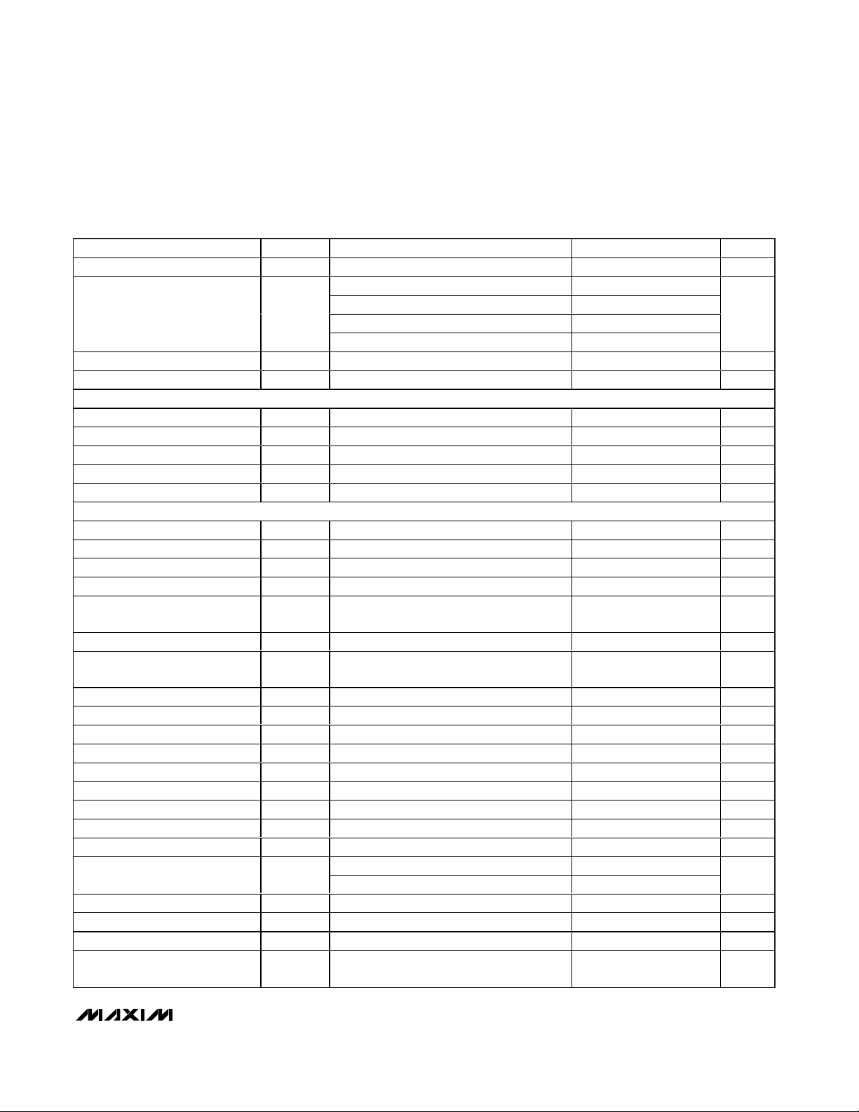
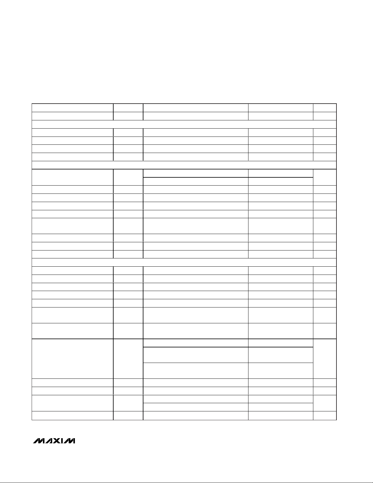
ELECTRICAL CHARACTERISTICS
(DVDD= 1.8V to 3.6V, AVDD= 2.7V to 5.5V, V
0.01µF capacitor at REFADJ; T
PARAMETER SYMBOL CONDITIONS MIN TYP MAX UNITS
ADC
MAX1329/MAX1330
Resolution No missing codes 12 Bits
DSP-Mode Resolution 256 oversampling, dither enabled 16 Bits
Integral Nonlinearity INL Normal mode (Note 1) ±1 LSB
Differential Nonlinearity DNL Normal mode (Note 1) ±1 LSB
Offset Error (Note 1) ±4 mV
Offset Drift ±1.5 µV/°C
Gain Error (Excluding Reference)
(Note 1)
Gain Temperature Coefficient Excluding reference ±0.8 ppm/°C
Voltage Range
Absolute Input Voltage Range AGND AV
Input Leakage Current into
Analog Inputs
Input Capacitance
Acquisition Time t
Conversion Time t
Conversion Clock Frequency 0.1 5.0 MHz
ADC Supply Current (Note 3)
Aperture Delay t
= T
A
MIN
to T
ACQ
CONV
AD
REFDAC
MAX
= V
, unless otherwise noted. Typical values are at TA= +25°C.)
Gain = 1 ±0.1
Gain = 2, 4 ±1.5
Gain = 8 ±2.5
Unipolar mode, gain = 1, 2, 4, 8 0
Bipolar mode, gain = 1, 2, 4, 8
(Note 2) ±0.5 ±1 nA
Gain = 1, 2 24
Gain = 4, 8 48
Gain = 1, 2 0.6
Gain = 4, 8 1.2
12 clocks 2.4 µs
Normal operation mode,
ADC converting at 234ksps
Fast power-down mode,
ADC converting at 234ksps
REFADC
AGND to DGND.................................................... -0.3V to +0.3V
Continuous Current into Any Pin.......................................±50mA
Continuous Power Dissipation (T
40-Pin Thin QFN (derate 37mW/°C above +70°C) ....2963mW
Operation Temperature Range............................-40°C to +85°C
Storage Temperature Range .............................-65°C to +150°C
Junction Temperature......................................................+150°C
Lead Temperature (soldering, 10s) ................................+300°C
= 2.5V, external reference; 10µF capacitor at REFADC and REFDAC;
-V
(2 x Gain)
A
REFADC
= +70°C)
+ V
R E F AD C
Gain
/
+ V
R E F AD C
(2 x Gain)
DD
325
210
30 ns
/
/
12
12
% FS
V
V
pF
µs
µA
2 _______________________________________________________________________________________
Page 3
MAX1329/MAX1330
12-/16-Bit DASs with ADC, DACs, DPIOs, APIOs,
Reference, Voltage Monitors, and Temp Sensor
_______________________________________________________________________________________ 3
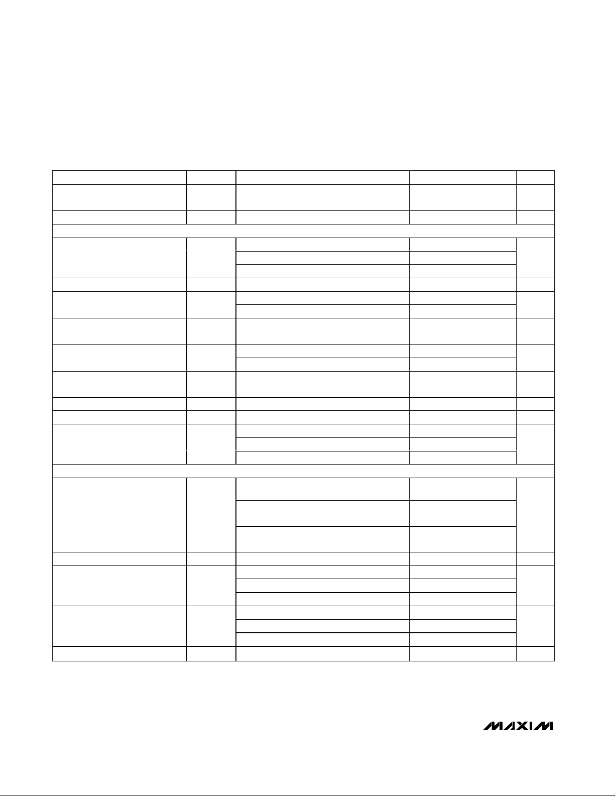
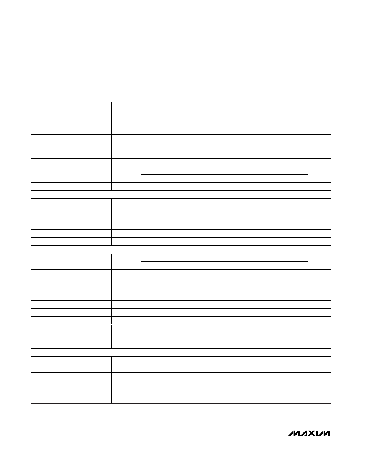
ELECTRICAL CHARACTERISTICS (continued)
(DVDD= 1.8V to 3.6V, AVDD= 2.7V to 5.5V, V
REFDAC
= V
REFADC
= 2.5V, external reference; 10µF capacitor at REFADC and REFDAC;
0.01µF capacitor at REFADJ; T
A
= T
MIN
to T
MAX
, unless otherwise noted. Typical values are at TA= +25°C.)
Aperture Jitter t
Sample Rate
Power-Supply Rejection PSR AVDD = 2.7V to 5.5V, full-scale input ±0.06 ±0.5 mV/V
Turn-On Time Supply and reference have settled 1 µs
ADC DYNAMIC ACCURACY (10kHz sine wave, VIN = 2.5V
Signal-to-Noise Plus Distortion SINAD 71 dB
Total Harmonic Distortion THD Up to the 5th harmonic 82 dB
Spurious-Free Dynamic Range SFDR 84 dB
Channel-to-Channel Crosstalk 100 dB
Full-Power Bandwidth FPBW -3dB point 4 MHz
DAC (R
Resolution 12 Bits
Differential Nonlinearity DNL Guaranteed monotonic (Note 4) ±1.0 LSB
Integral Nonlinearity INL (Note 4) ±1 ±8 LSB
Offset Error Code = 0x000 (tested at 0x032) ±2.5 ±30 mV
Offset-Error Temperature
Coefficient
Gain Error Code = 0xFFF 0 ±5 % FS
Gain-Error Temperature
Coefficient
Output Voltage Range No load AGND AV
Output Slew Rate CL = 200pF 0.5 V/µs
Output Settling Time Code = 0x400 to 0xC00 (Note 2) 4 10 µs
FB_ Input Bias Current (Note 2) ±0.1 1 nA
FB_ Switch Resistance 200 Ω
FB_ Switch Turn-On/-Off Time 40 ns
FB_ Switch Off Isolation f = 10kHz 100 dB
FB_ Switch Charge Injection 1pC
DAC-to-DAC Crosstalk 0.5 nV-s
Short-Circuit Current
DC Output Impedance Code = 0x800 0.8 Ω
Power-Up Time 0.5 LSB settling to 0x800 5 µs
Power-Supply Rejection PSR AVDD = 2.7V to 5.5V ±1 mV/V
Charge-Pump Output
Feedthrough
PARAMETER SYMBOL CONDITIONS MIN TYP MAX UNITS
= 5kΩ, C
L
= 200pF, tested in unity gain, unless otherwise noted)
L
AJ
Gain = 1, 2; DVDD ≥ 2.7V, AVDD ≥ 5.0V 312
Gain = 4, 8; DVDD ≥ 2.7V, AVDD ≥ 5.0V 263
Gain = 1, 2 234
Gain = 4, 8 200
Due to amplifier ±7 µV/°C
Excluding reference drift ±7 ppm/°C
Sink 13
Source 50
Code = 0x800, buffer on, RL = 5kΩ,
= 200pF
C
L
50 ps
P-P
, f
= 234ksps, gain = 1)
SAMPLE
DD
100 µV
ksps
V
mA
RMS
Page 4
MAX1329/MAX1330
12-/16-Bit DASs with ADC, DACs, DPIOs, APIOs,
Reference, Voltage Monitors, and Temp Sensor
4 _______________________________________________________________________________________
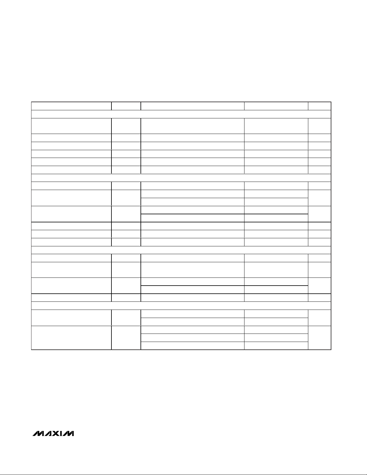
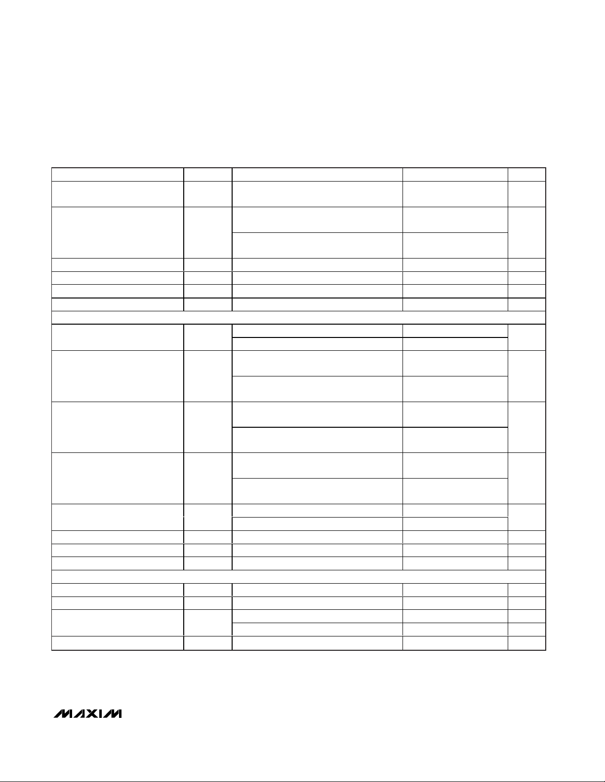
ELECTRICAL CHARACTERISTICS (continued)
(DVDD= 1.8V to 3.6V, AVDD= 2.7V to 5.5V, V
REFDAC
= V
REFADC
= 2.5V, external reference; 10µF capacitor at REFADC and REFDAC;
0.01µF capacitor at REFADJ; T
A
= T
MIN
to T
MAX
, unless otherwise noted. Typical values are at TA= +25°C.)
Power-Down Output Leakage
Current
Supply Current per DAC No load (Note 3) 70 µA
INTERNAL REFERENCE (10µF capacitor at REFADC and REFDAC, 0.01µF capacitor at REFADJ)
Output Voltage at REFADC and
REFDAC
Output-Voltage Temperature
REFADC and REFDAC
Output Short-Circuit Current
REFADC and REFDAC
Line Regulation
PARAMETER SYMBOL CONDITIONS MIN TYP MAX UNITS
Load Regulation
Long-Term Stability TA = +25°C ±100
Turn-On Time At REFADJ 2 ms
Turn-Off Time 100 ns
Refer ence S up p l y C ur r ent ( N ote 3)
EXTERNAL REFERENCE AT REFADJ
External Reference Input Voltage
Range
Input Resistance 50 75 kΩ
Minimum Capacitive Bypass REFADJ to AGND 10 nF
TA = + 25° C , ARE F< 1:0> = D RE F< 1:0> = 01 1.225 1.250 1.275
TA = + 25° C , ARE F< 1:0> = D RE F< 1:0> = 10 2.007 2.048 2.089
= + 25° C , ARE F< 1:0> = D RE F< 1:0> = 11 2.450 2.500 2.550
T
A
(Note 2) ±10 ±75 ppm/°C
Source 40
Sink 13
I
SOURCE
= 0µA to 80µA, T
I
SINK
Internal reference 445
REFADC buffer 270
REFDAC buffer 270
AREF<1:0> = DREF<1:0> = 11 1.225V
AREF<1:0> = DREF<1:0> = 10
AREF<1:0> = DREF<1:0> = 01
AREF<1:0> = 01 1
AREF<1:0> = 10 0.8192REFADC Buffer Gain
AREF<1:0> = 11 0.5
DREF<1:0> = 01 1
DREF<1:0> = 10 0.8192REFDAC Buffer Gain
DREF<1:0> = 11 0.5
±100 nA
±100 ±600 µV/V
= 0µA to 500µA, TA = +25°C 10
= +25°C 10
A
AV
- 0.1V
1.496V to
AV
- 0.1V
DD
2.450V to
AV
- 0.1V
DD
DD
V
mA
µV/µA
ppm/
1000hrs
µA
V
V/V
V/V
Page 5
MAX1329/MAX1330
12-/16-Bit DASs with ADC, DACs, DPIOs, APIOs,
Reference, Voltage Monitors, and Temp Sensor
_______________________________________________________________________________________ 5
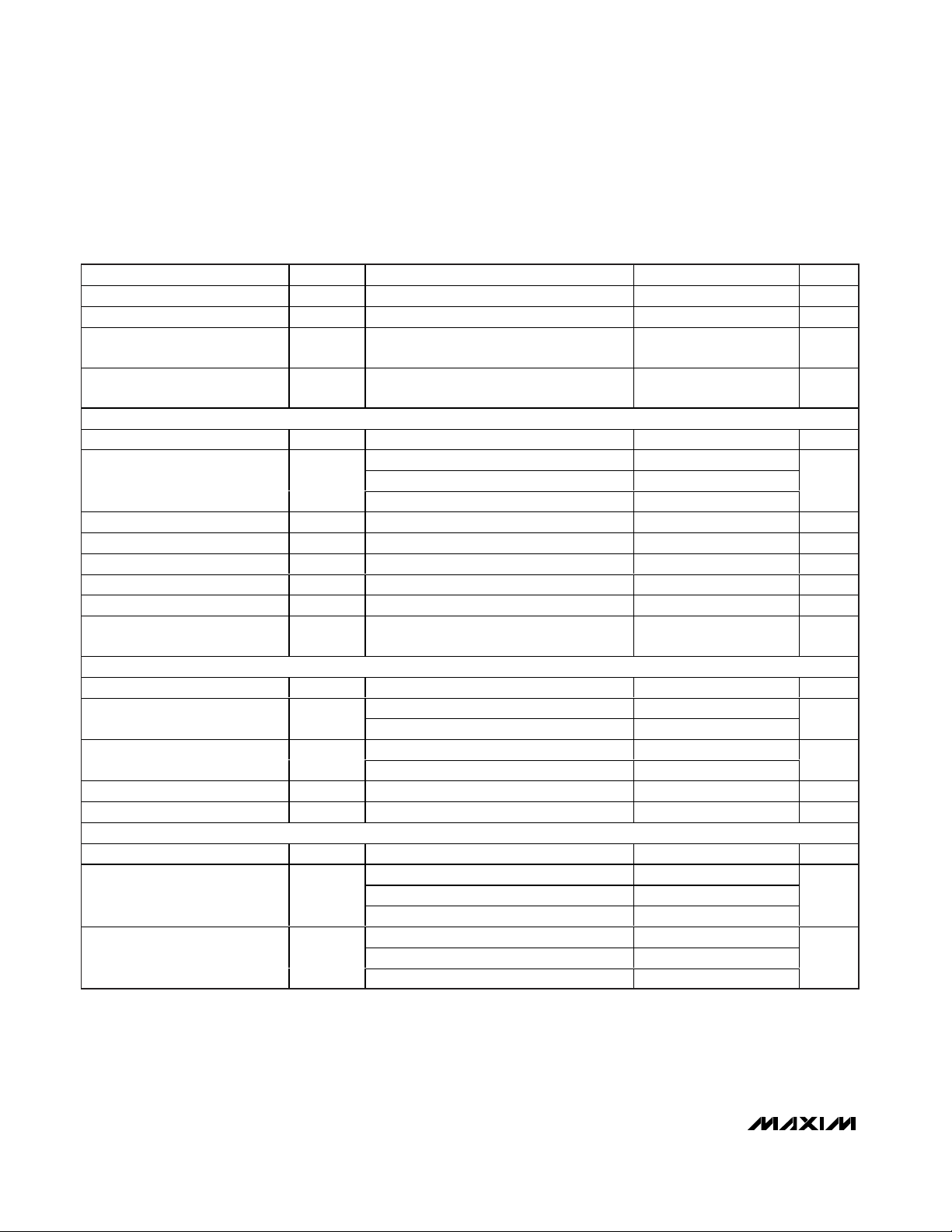
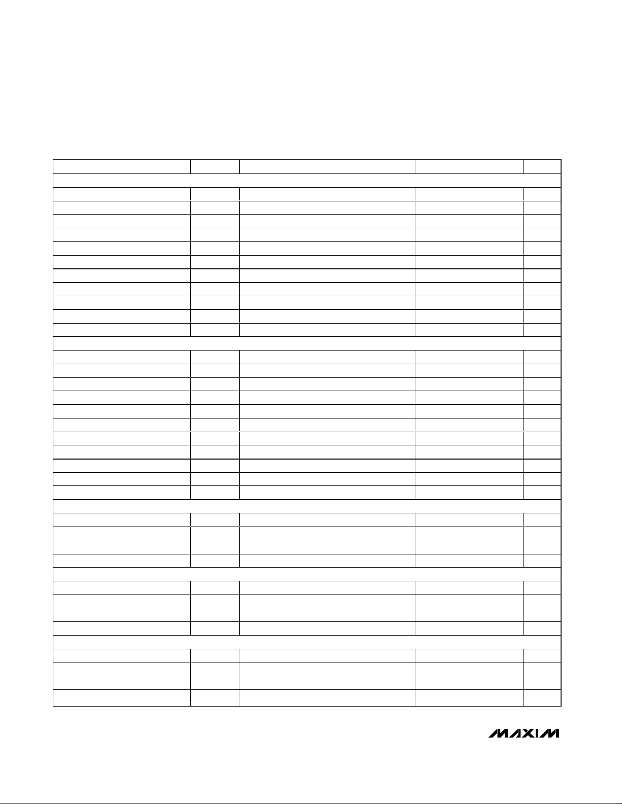
ELECTRICAL CHARACTERISTICS (continued)
(DVDD= 1.8V to 3.6V, AVDD= 2.7V to 5.5V, V
REFDAC
= V
REFADC
= 2.5V, external reference; 10µF capacitor at REFADC and REFDAC;
0.01µF capacitor at REFADJ; T
A
= T
MIN
to T
MAX
, unless otherwise noted. Typical values are at TA= +25°C.)
EXTERNAL REFERENCE AT REFADC
External Reference Input Voltage
Range
REFADC Input Resistance 50 75 kΩ
REFADC Input Current V
Turn-On Time REFADC buffer, C
Shutdown REFADC Input Current 0.01 1.0 µA
Minimum Capacitive Bypass REFADC to AGND 10 µF
EXTERNAL REFERENCE AT REFDAC
REFDAC Input Voltage Range AGND AV
REFDAC Input Resistance
REFDAC Input Current
Turn-On Time REFDAC buffer 75 µs
Shutdown REFDAC Input Current 0.1 1 µA
Minimum Capacitive Bypass REFDAC to AGND 10 µF
MULTIPLEXER
Absolute Input Voltage Range AGND AV
Absolute Input Leakage Current
Input Capacitance
On Resistance 340 Ω
INTERNAL TEMPERATURE SENSOR
Internal Sensor Measurement
Error ( N ote 5)
External Sensor Measurement
Error ( N ote 5)
PARAMETER SYMBOL CONDITIONS MIN TYP MAX UNITS
REFADC
MAX1329 64 90 180
MAX1330 128 180 360
MAX1329, V
MAX1330, V
( AG N D + 100m V ) < V
( N ote 2)
ADC gain = 1, 2 24
ADC gain = 4, 8 48
TA = +25°C ±0.25
T
= -40°C to +85°C ±3
A
TA = +25°C ±0.4
TA = 0°C to +70°C ±2
T
= -40°C to +85°C ±3
A
AGND AV
= 2.5V, 300ksps 30 40 µA
= 1µF 75 µs
REFADC
= 2.5V 28 86
REFDAC
= 2.5V 14 43
REFDAC
A IN _
< ( AV
- 100m V )
D D
±0.01 ±1 nA
DD
DD
DD
V
V
kΩ
µA
V
pF
°C
°C
Page 6
MAX1329/MAX1330
12-/16-Bit DASs with ADC, DACs, DPIOs, APIOs,
Reference, Voltage Monitors, and Temp Sensor
6 _______________________________________________________________________________________
ELECTRICAL CHARACTERISTICS (continued)
(DVDD= 1.8V to 3.6V, AVDD= 2.7V to 5.5V, V
REFDAC
= V
REFADC
= 2.5V, external reference; 10µF capacitor at REFADC and REFDAC;
0.01µF capacitor at REFADJ; T
A
= T
MIN
to T
MAX
, unless otherwise noted. Typical values are at TA= +25°C.)
Temperature Resolution V
External-Diode Drive Ratio I
Temperature-Sensor Supply
Current
Temperature-Sensor Conversion
Time
CHARGE PUMP
Input Voltage DV
No-Load Output Voltage AV
Output Current Including internal current (Table 32) 25 mA
No-Load Supply Current DVDD = 2.7V, AVDD = 4V, 39kHz clock 250 µA
Switching Frequency 39 78 kHz
Switch Turn-On/-Off Time Between DVDD to AVDD, charge pump off 40 ns
Switch Impedance Shorts DV
Efficiency
DVDD VOLTAGE MONITOR (VM1)
Supply Voltage Range 1.0 3.6 V
Trip Threshold (DV
Hysteresis V
Reset Timeout Period V
Turn-On Time DVDD = 1.8V, enabled by VM1 <1:0> 2 ms
AVDD VOLTAGE MONITOR (VM2)
Supply Voltage Range 1.0 5.5 V
Trip Threshold (AVDD Falling)
(Note 6)
Hysteresis V
PARAMETER SYMBOL CONDITIONS MIN TYP MAX UNITS
Falling) V
DD
DTH
DHYS
V
ATH
AHYS
DD
DD
= 2.5V 1/8 °C/LSB
REFADC
DRIVEMIN
Not including ADC current (Note 3) 100 µA
307 clocks per measurement, master clock
= 5.00MHz
DV
DV
DV
25mA load, DV
39kHz clock
VM1<1:0> = 0x, RST1 input 1.80 1.865 1.93
VM1<1:0> = x0, RST2 input 2.65 2.750 2.90
VM1<1:0> = 0x, RST1 input 15
VM1<1:0> = x0, RST2 input 22.5
DVDD
VM2CP<1:0> = 01 2.53 2.775 2.975
VM2CP<1:0> = 10 3.4 3.700 3.925
VM2CP<1:0> = 11 4.25 4.625 4.925
VM2CP<1:0> = 01 22.5
VM2CP<1:0> = 10 30
VM2CP<1:0> = 11 37.5
= 4µA, I
= 1.8V to 3.0V, VM2CP<2:0> = 001 2.85 3.0 3.20
DD
= 2.2V to 3.6V, VM2CP<2:0> = 010 3.75 4.0 4.30
DD
= 2.7V to 3.6V, VM2CP<2:0> = 011 4.80 5.0 5.40
DD
DD
= V
DRIVEMAX
to AVDD, charge pump off 25 50 Ω
= 1.8V, AVDD = 3.0V,
DD
+ V
DTH
DHYS
= 68µA 17:1
65 µs
1.8 3.6 V
80 %
170 ms
V
V
mV
V
mV
Page 7
MAX1329/MAX1330
12-/16-Bit DASs with ADC, DACs, DPIOs, APIOs,
Reference, Voltage Monitors, and Temp Sensor
_______________________________________________________________________________________ 7
ELECTRICAL CHARACTERISTICS (continued)
(DVDD= 1.8V to 3.6V, AVDD= 2.7V to 5.5V, V
REFDAC
= V
REFADC
= 2.5V, external reference; 10µF capacitor at REFADC and REFDAC;
0.01µF capacitor at REFADJ; T
A
= T
MIN
to T
MAX
, unless otherwise noted. Typical values are at TA= +25°C.)
Turn-On Time AVDD = 2.7V, enabled by VM2CP<1:0> 2 ms
INTERNAL OSCILLATOR
Clock Frequency TA = T
Turn-Off Delay Using clock at CLKIO pin, ODLY = 1 1024 Clocks
Turn-On Time 200 ns
Supply Current (Note 7) 120 µA
SWITCHES (SPDT)
On Resistance
On-Resistance Match 15 Ω
On-Resistance Flatness Over analog voltage range 12 Ω
Analog Voltage Range AGND AV
Turn-On/-Off Time Break-before-make for SPDT configuration 50 ns
Leakage Current
Off Isolation f = 10kHz 100 dB
Charge Injection 1pC
Input Capacitance 2pF
OPERATIONAL AMPLIFIER (R
Input Bias Current (Note 2) 0.3 ±1 nA
Input Offset Voltage V
Input Offset Drift ∆V
Common-Mode Rejection Ratio CMRR AGND + 100mV < VCM < AVDD - 100mV 75 dB
Phase Margin 60 degrees
Charge-Pump Output
Feedthrough
Common-Mode Input Voltage
Range
Output Voltage Range
Gain Bandwidth Product 1 MHz
Slew Rate 0.5 V/µs
OSW_ Switch Resistance
OSW_ Switch Turn-On/-Off Time 50 ns
PARAMETER SYMBOL CONDITIONS MIN TYP MAX UNITS
= 10kΩ, C
L
OS
L
OS
to T
MIN
MAX
AV
= 2.7V to 5.5V 140 200
DD
AV
= 4.5V to 5.5V 90 120
DD
AGND + 100mV < V
(Note 2)
= 200pF)
No load AGND AV
10kΩ load 0.1
100kΩ load 0.1
AV
= 2.7V to 5.5V 140 200
DD
= 4.5V to 5.5V 90 120
AV
DD
< AVDD - 100mV
SN_
3.5758 3.6864 3.7970 MHz
0.08 ±1 nA
2 ±20 mV
±10 µV/°C
100 µV
AGND AV
AV
- 0.1
AV
- 0.1
DD
DD
DD
DD
DD
Ω
V
P-P
V
V
Ω
Page 8
MAX1329/MAX1330
12-/16-Bit DASs with ADC, DACs, DPIOs, APIOs,
Reference, Voltage Monitors, and Temp Sensor
8 _______________________________________________________________________________________
ELECTRICAL CHARACTERISTICS (continued)
(DVDD= 1.8V to 3.6V, AVDD= 2.7V to 5.5V, V
REFDAC
= V
REFADC
= 2.5V, external reference; 10µF capacitor at REFADC and REFDAC;
0.01µF capacitor at REFADJ; T
A
= T
MIN
to T
MAX
, unless otherwise noted. Typical values are at TA= +25°C.)
OSW_ Switch Charge Injection 1pC
Input Noise Voltage Density f
Input Noise Voltage f
Power-Down Output Leakage ±10 nA
Power-Supply Rejection Ratio AVDD = 2.7V to 5.5V 65 100 dB
Supply Current per Amplifier (Note 3) 70 µA
Turn-On Time 5µs
Short-Circuit Current
DC Output Impedance A
DIGITAL INPUTS (DIN, SCLK, CS)
Input High Voltage V
Input Low Voltage V
Input Hysteresis DVDD = 3V 200 mV
Input Leakage Current VIN = 0 or DV
DIGITAL OUTPUTS (DOUT, RST1, RST2)
Output Low Voltage V
Output High Voltage V
DOUT Three-State Leakage ±0.01 ±10 µA
DOUT Three-State Capacitance (Note 2) 15 pF
RST1, RST2 Open-Drain Output
Low Voltage
RST1, RST2 Open-Drain Output
Leakage Current
DIGITAL I/O (DPIO1–DPIO4, CLKIO)
Output Low Voltage
Output High Voltage
PARAMETER SYMBOL CONDITIONS MIN TYP MAX UNITS
OL
OH
IH
IL
= 1kHz 330 nV/√Hz
IN_
= 0.1Hz to 10Hz 9 µV
IN_
Source 50
Sink 13
= 1V/V 0.2 Ω
V
0.7 x
DV
DD
0.3 x
DV
DD
DD
I
= 1mA, DVDD = 2.7V to 3.6V 0.4
SINK
I
= 200µA, DVDD = 1.8V to 3.6V 0.4
SINK
I
I
I
I
(Note 2) 0.13 100 nA
I
I
I
I
= 0.2mA, DVDD = 2.7V to 3.6V
SOURCE
= 100µA, DVDD = 1.8V to 3.6V
SOURCE
= 1mA, DVDD = 2.7V to 3.6V 0.4
SINK
= 200µA, DVDD = 1.8V to 3.6V 0.4
SINK
= 2mA, DVDD = 2.7V to 3.6V 0.4
SINK
= 1mA, DVDD = 1.8V to 3.6V 0.4
SINK
= 2mA, DVDD = 2.7V to 3.6V
SOURCE
= 1mA, DVDD = 1.8V to 3.6V
SOURCE
0.8 x
DV
0.8 x
DV
0.8 x
DV
0.8 x
DV
±0.01 ±10 µA
DD
DD
DD
DD
RMS
mA
V
V
V
V
V
V
V
Page 9
MAX1329/MAX1330
12-/16-Bit DASs with ADC, DACs, DPIOs, APIOs,
Reference, Voltage Monitors, and Temp Sensor
_______________________________________________________________________________________ 9
ELECTRICAL CHARACTERISTICS (continued)
(DVDD= 1.8V to 3.6V, AVDD= 2.7V to 5.5V, V
REFDAC
= V
REFADC
= 2.5V, external reference; 10µF capacitor at REFADC and REFDAC;
0.01µF capacitor at REFADJ; T
A
= T
MIN
to T
MAX
, unless otherwise noted. Typical values are at TA= +25°C.)
Input High Voltage
Input Low Voltage
Input Hysteresis DVDD = 3V 110 mV
Three-State Leakage ±0.01 ±1 µA
Three-State Capacitance (Note 2) 15 pF
DPIO_ Pullup Resistance 0.5 MΩ
ANALOG I/O (APIO1–APIO4)
Output Low Voltage
Output High Voltage
Input High Voltage
Input Low Voltage
Input Hysteresis
Three-State Leakage ±0.01 ±10 µA
Three-State Capacitance (Note 2) 15 pF
Pullup Resistance 0.5 MΩ
POWER REQUIREMENTS
DV
AV
Supply Current (Note 8)
Shutdown Current All off 0.5 1 µA
PARAMETER SYMBOL CONDITIONS MIN TYP MAX UNITS
Supply Voltage Range 1.8 3.6 V
DD
Supply Voltage Range 2.7 5.5 V
DD
0.7 x
DV
DD
DPIO1–DPIO4
CLKIO
I
= 2mA, AV
SINK
I
= 1mA, AVDD = 1.8V to 5.5V 0.4
SINK
I
I
AVDD = 2.7V to 5.5V
AV
AVDD = 2.7V to 5.5V
AV
AVDD = 3V 120
AV
Run (all on, except charge pump) 3.75 7.5 mA
Sleep (1.8V or 2.7V monitor on) 1 2.5 µA
= 2mA, AVDD = 2.7V to 5.5V
SOURCE
= 1mA, AVDD = 1.8V to 5.5V
SOURCE
= DVDD = 1.8V to 3.6V
DD
= DVDD = 1.8V to 3.6V
DD
= 5V 160
DD
= 2.7V to 5.5V 0.4
DD
0.8 x
AV
DD
0.8 x
AV
DD
0.7 x
AV
DD
0.7 x
AV
DD
0.3 x
DV
DD
0.25 x
DV
DD
0.3 x
AV
DD
0.3 x
AV
DD
V
V
V
V
V
V
mV
Page 10
MAX1329/MAX1330
12-/16-Bit DASs with ADC, DACs, DPIOs, APIOs,
Reference, Voltage Monitors, and Temp Sensor
10 ______________________________________________________________________________________
TIMING CHARACTERISTICS
(DVDD= 1.8V to 3.6V, AVDD= 2.7V to 5.5V, TA= T
MIN
to T
MAX
, unless otherwise noted.)
PARAMETER SYMBOL CONDITIONS MIN TYP MAX UNITS
SERIAL-INTERFACE TIMING PARAMETERS (DV
SCLK Operating Frequency
SCLK Cycle Time
DIN to SCLK Setup
DIN to SCLK Hold
SCLK Fall to Output Data Valid
CS Fall to Output Enable
CS Rise to Output Disable
CS to SCLK Rise Setup
CS to SCLK Rise Hold
SCLK Pulse-Width High
SCLK Pulse-Width Low
SERIAL-INTERFACE TIMING PARAMETERS (DV
SCLK Operating Frequency
SCLK Cycle Time
DIN to SCLK Setup
DIN to SCLK Hold
SCLK Fall to Output Data Valid
CS Fall to Output Enable
CS Rise to Output Disable
CS to SCLK Rise Setup
CS to SCLK Rise Hold
SCLK Pulse-Width High
SCLK Pulse-Width Low
f
t
CYC
t
t
t
t
t
t
CSS
t
CSH
t
t
f
t
CYC
t
t
t
t
t
t
CSS
t
CSH
t
t
OP
DS
DH
DO
DV
TR
CH
CL
OP
DS
DH
DO
DV
TR
CH
CL
DIGITAL PROGRAMMABLE I/O TIMING PARAMETERS (DPIO1–DPIO4, DV
SPI Write to DPIO Output Valid
DPIO Rise/Fall Input to Interrupt
Asserted Delay
DPIO Input to Analog Block Delay
t
SD
t
DI
t
DA
DIGITAL PROGRAMMABLE I/O TIMING PARAMETERS (DPIO1–DPIO4, DV
SPI Write to DPIO Output Valid
DPIO Rise/Fall Input to Interrupt
Asserted Delay
DPIO Input to Analog Block Delay
t
SD
t
DI
t
DA
ANALOG PROGRAMMABLE I/O TIMING PARAMETERS (APIO1–APIO4, DV
SPI Write to APIO Output Valid
APIO Rise/Fall Input to Interrupt
Asserted Delay
CS to APIO4 Propagation Delay
t
t
DCA
t
SD
DI
DD
= 2.7V to 3.6V) (Figures 1 and 2)
0 20 MHz
50 ns
15 ns
0ns
20 ns
24 ns
24 ns
15 ns
0ns
20 ns
20 ns
= 1.8V to 3.6V) (Figures 1 and 2)
DD
0 10 MHz
100 ns
30 ns
0ns
40 ns
48 ns
48 ns
30 ns
0ns
40 ns
40 ns
= 2.7V to 3.6V, CL =
DD
20pF)
From last SCLK rising edge 50 ns
Interrupt programmed on RST1 and/or
RST2, corresponding status bits unmasked
55 ns
When controlling ADC, DACs, or switches 40 ns
= 1.8V to 3.6V, CL =
DD
20pF)
From last SCLK rising edge 100 ns
Interrupt programmed on RST1 and/or
RST2, corresponding status bits unmasked
150 ns
When controlling ADC, DACs, or switches 50 ns
= 2.7V to 3.6V, AVDD = 2.7V to 5.5V, CL =
DD
From last SCLK rising edge 50 ns
Interrupt programmed on RST1 and/or
RST2, corresponding status bits unmasked
50 ns
AP4MD<1:0> = 11 35 ns
20pF)
Page 11
MAX1329/MAX1330
12-/16-Bit DASs with ADC, DACs, DPIOs, APIOs,
Reference, Voltage Monitors, and Temp Sensor
______________________________________________________________________________________ 11
TIMING CHARACTERISTICS (continued)
(DVDD= 1.8V to 3.6V, AVDD= 2.7V to 5.5V, TA= T
MIN
to T
MAX
, unless otherwise noted.)
Note 1: ADC INL and DNL, offset, and gain are tested at DVDD= 1.8V, AVDD= 2.7V, f
SAMPLE
= 234ksps to guarantee performance
at f
SAMPLE
= 312ksps, DVDD≥ 2.7V and AVDD≥ 5.0V.
Note 2: Guaranteed by design. Not production tested.
Note 3: AV
DD
supply current contribution for this module.
Note 4: DNL and INL are measured between code 115 and 4095.
Note 5: Temperature sensor accuracy is tested using a 2.5084V reference applied to REFADJ.
Note 6: The maximum trip levels for the AV
DD
monitor are 5% below the typical charge-pump output value. The charge-pump output
voltage and the trip thresholds track to prevent tripping at -5% below the typical charge-pump output value.
Note 7: DV
DD
supply current contribution for this module.
Note 8: The normal operation and sleep mode supply currents are measured with no load on DOUT, SCLK idle, and all digital inputs
at DGND or DV
DD
. CLKIO runs in normal mode operation and idle in sleep mode.
SCLK to APIO3 Propagation
Delay
DIN to APIO2 Propagation Delay
APIO1 to DOUT Propagation
Delay
SPI-Mode Propagation Delay
Matching
ANALOG PROGRAMMABLE I/O TIMING PARAMETERS (APIO1–APIO4, DV
SPI Write to APIO Output Valid
APIO Rise/Fall Input to Interrupt
Asserted Delay
CS to APIO4 Propagation Delay
SCLK to APIO3 Propagation
Delay
DIN to APIO2 Propagation Delay
APIO1 to DOUT Propagation
Delay
SPI-Mode Propagation Delay
Matching
PARAMETER SYMBOL CONDITIONS MIN TYP MAX UNITS
t
DSA
t
DDA
t
DAD
t
DM
t
SD
t
DI
t
DCA
t
DSA
t
DDA
t
DAD
t
DM
AP3MD<1:0> = 11, CS is high 30 ns
AP2MD<1:0> = 11, CS is high 25 ns
AP1MD<1:0> = 11, CS is high 20 ns
Among APIO4, APIO3, APIO2, and APIO1 ±10 ns
From last SCLK rising edge 100 ns
Interrupt programmed on RST1 and/or
RST2, corresponding status bits unmasked
AP4MD<1:0> = 11 60 ns
AP3MD<1:0> = 11, CS is high 50 ns
AP2MD<1:0> = 11, CS is high 50 ns
AP1MD<1:0> = 11, CS is high 80 ns
Among APIO4, APIO3, APIO2, and APIO1 ±30 ns
= 1.8V to 3.6V, AVDD = 2.7V to 5.5V, CL = 20pF)
DD
175 ns
Page 12
MAX1329/MAX1330
12-/16-Bit DASs with ADC, DACs, DPIOs, APIOs,
Reference, Voltage Monitors, and Temp Sensor
12 ______________________________________________________________________________________
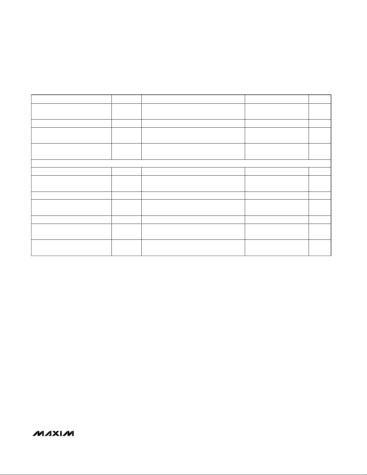
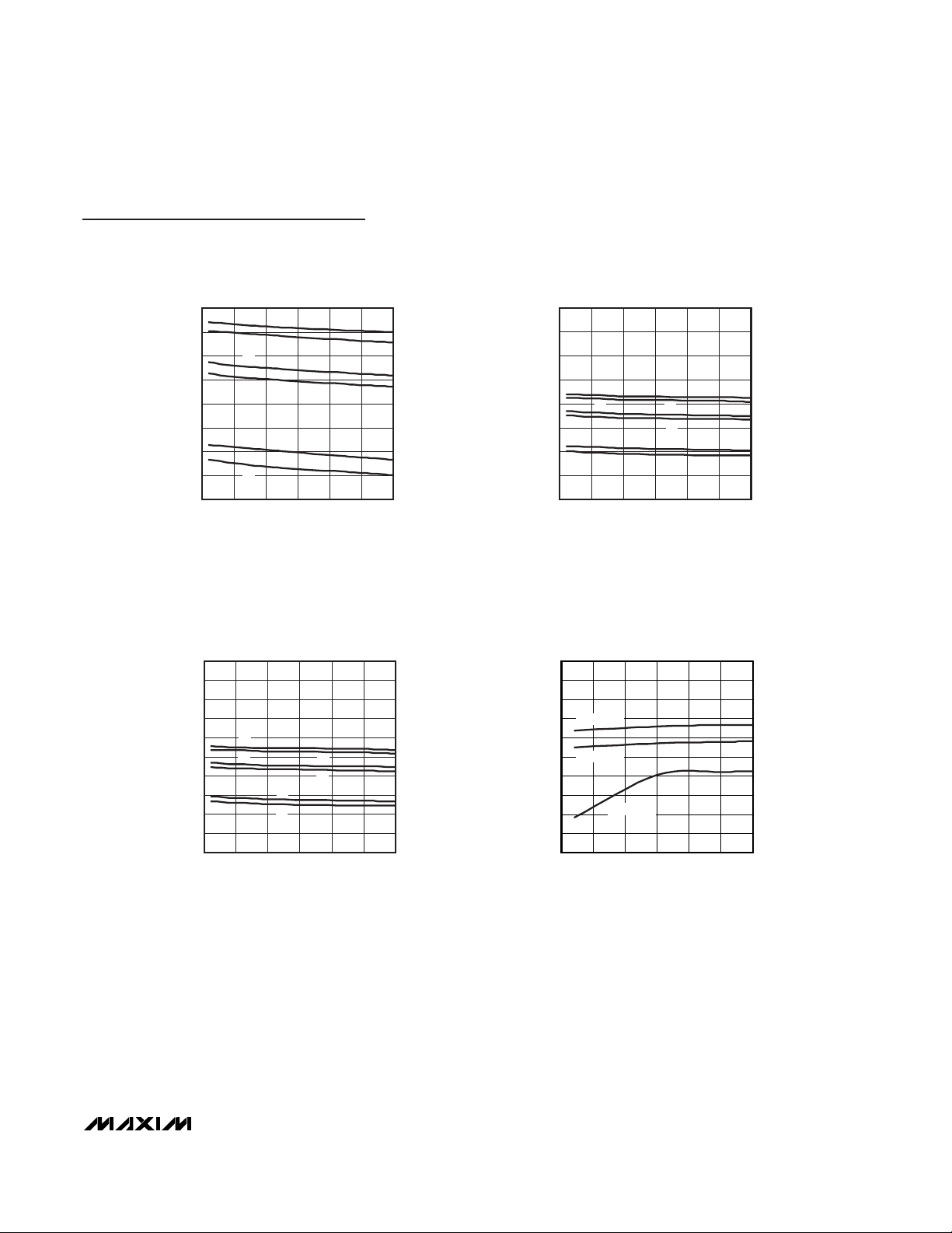
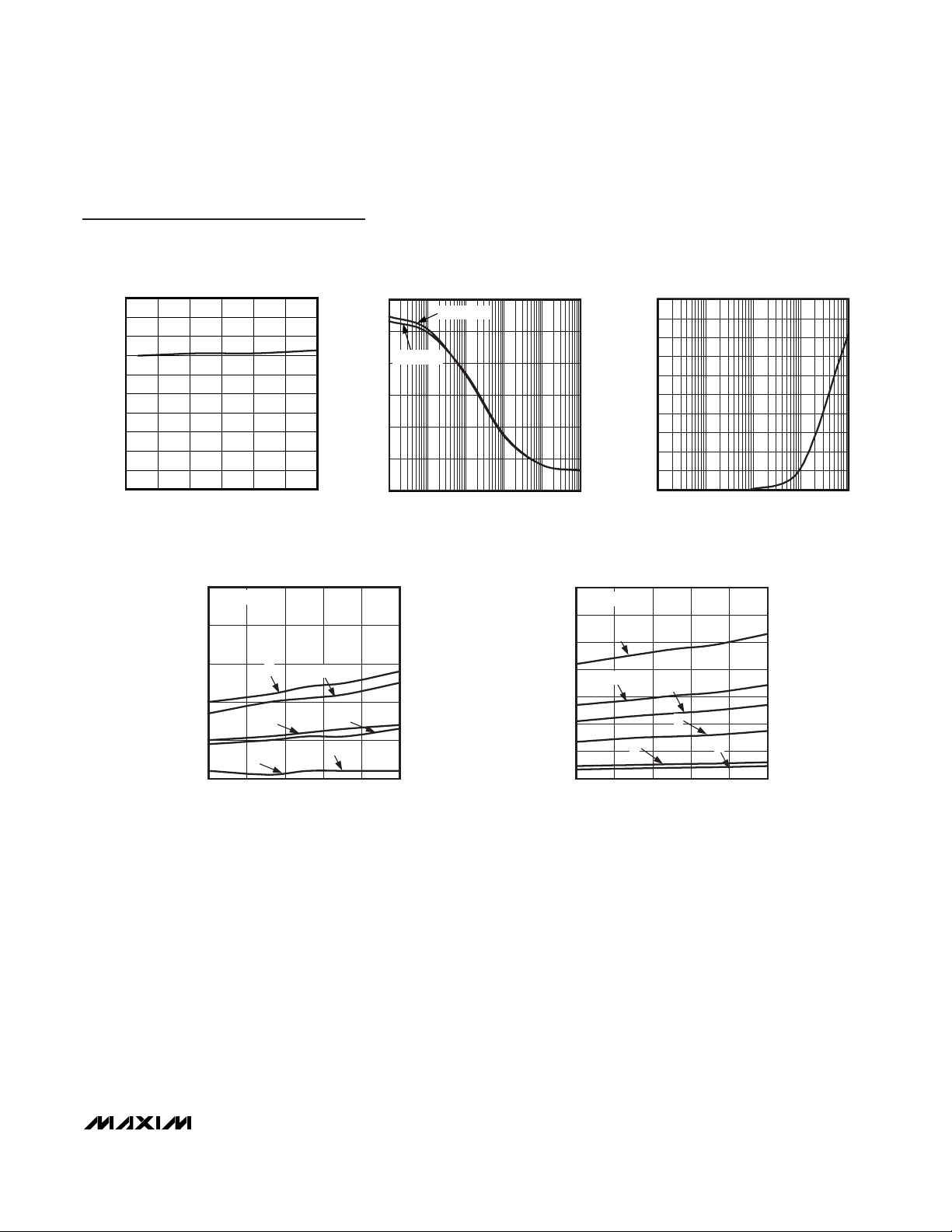
Typical Operating Characteristics
(AVDD= 5.0V, V
REFADC
= V
REFDAC
= 2.5V for DVDD= 3.0V; TA= +25°C, unless otherwise noted.)
0
0.50
0.25
1.00
0.75
1.25
1.50
1.75
2.00
1.5 2.5 3.02.0 3.5 4.0 4.5 5.0 5.5
STATIC DIGITAL SUPPLY CURRENT
vs. DIGITAL SUPPLY VOLTAGE (ONLY VM1A ON)
MAX1329 toc02
DVDD (V)
I
DVDD
(μA)
TA = +25°C
TA = +85°C
TA = -40°C
f
OSC
ERROR
vs. DIGITAL SUPPLY VOLTAGE
MAX1329 toc07
DVDD (V)
f
OSC
ERROR (%)
3.43.22.8 3.02.2 2.4 2.62.0
-0.8
-0.6
-0.4
-0.2
0
0.2
0.4
0.6
0.8
1.0
-1.0
1.8 3.6
NOMINAL f
OSC
= 3.6864MHz (0% VALUE)
TA = -40°C
TA = +85°C
TA = +25°C
ADC INTEGRAL NONLINEARITY
vs. TEMPERATURE
MAX1329 toc08
TEMPERATURE (°C)
INL (LSB)
603510-15
0.3
0.4
0.5
0.6
0.7
0.8
0.2
-40 85
f
CONV
= 234ksps
AVDD = 2.7V
AVDD = 5.5V
AVDD = 5.0V
ADC INTEGRAL NONLINEARITY
vs. TEMPERATURE
MAX1329 toc09
TEMPERATURE (°C)
INL (LSB)
603510-15
0.3
0.4
0.5
0.6
0.7
0.8
0.2
-40 85
AVDD = 5.5V
AVDD = 5.0V
f
CONV
= 312ksps
STATIC DIGITAL SUPPLY CURRENT
vs. DIGITAL SUPLY VOLTAGE (EVERYTHING ON)
1.0
0.8
TA = +85°C
0.6
(mA)
DVDD
I
0.4
0.2
0
1.5 2.5 3.02.0 3.5 4.0 4.5 5.0 5.5
TA = +25°C
DVDD (V)
TA = -40°C
vs. DIGITAL SUPPLY VOLTAGE (SHUTDOWN)
2.00
(μA)
DVDD
I
1.75
1.50
1.25
1.00
0.75
0.50
0.25
0
MAX1329 toc01
STATIC DIGITAL SUPPLY CURRENT
TA = +85°C
1.5 2.5 3.02.0 3.5 4.0 4.5 5.0 5.5
TA = +25°C
TA = -40°C
DVDD (V)
STATIC ANALOG SUPPLY CURRENT
vs. ANALOG SUPPLY VOLTAGE (EVERYTHING ON)
1.70
1.65
1.60
1.55
(mA)
1.50
AVDD
I
1.45
1.40
1.35
1.30
2.5 3.53.0 4.0 4.5 5.0 5.5
TA = -40°C
TA = +85°C
TA = +25°C
AVDD (V)
STATIC ANALOG SUPPLY CURRENT vs. ANALOG
SUPPLY VOLTAGE (ONLY VM1A AND VM1B ON)
1000
MAX1329 toc04
800
600
(nA)
AVDD
I
400
200
0
2.5 3.53.0 4.0 4.5 5.0 5.5
TA = +85°C
TA = +25°C
TA = -40°C
AVDD (V)
MAX1329 toc05
STATIC ANALOG SUPPLY CURRENT
vs. ANALOG SUPPLY VOLTAGE (SHUTDOWN)
1000
TA = +85°C
TA = +25°C
TA = -40°C
2.5 3.53.0 4.0 4.5 5.0 5.5
AVDD (V)
(nA)
AVDD
I
800
600
400
200
0
MAX1329 toc03
MAX1329 toc06
Page 13
MAX1329/MAX1330
12-/16-Bit DASs with ADC, DACs, DPIOs, APIOs,
Reference, Voltage Monitors, and Temp Sensor
______________________________________________________________________________________ 13
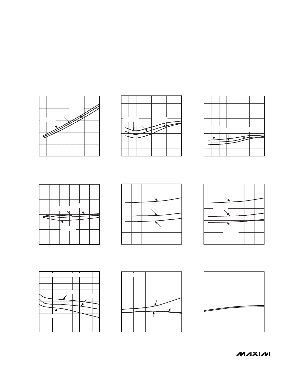
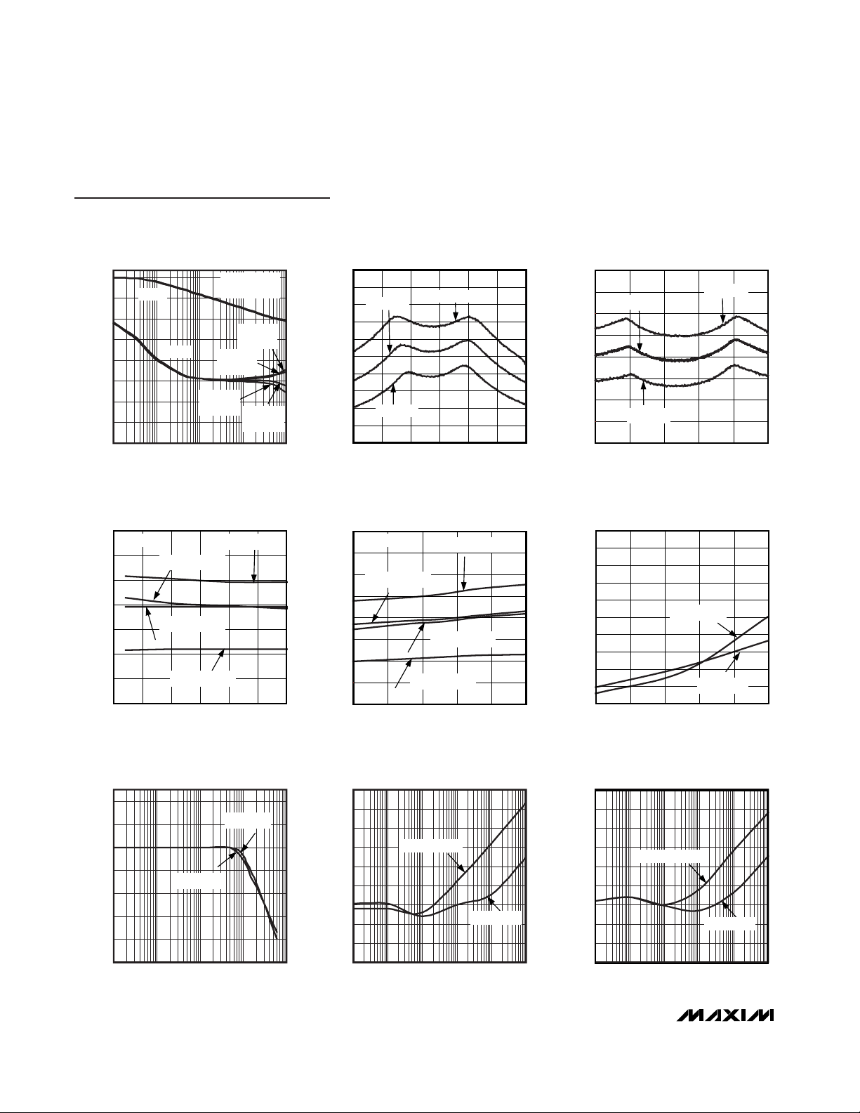
Typical Operating Characteristics (continued)
(AVDD= 5.0V, V
REFADC
= V
REFDAC
= 2.5V for DVDD= 3.0V; TA= +25°C, unless otherwise noted.)
ADC DIFFERENTIAL NONLINEARITY
vs. DIGITAL INPUT CODE (AV
DD
= 3.0V)
MAX1329 toc10
DIGITAL INPUT CODE
DNL (LSB)
307220481024
-0.8
-0.6
-0.4
-0.2
0
0.2
0.4
0.6
0.8
1.0
-1.0
0 4096
f
SAMPLE
= 234ksps
ADC INTEGRAL NONLINEARITY
vs. DIGITAL INPUT CODE (AV
DD
= 3.0V)
MAX1329 toc11
DIGITAL INPUT CODE
INL (LSB)
307220481024
-0.8
-0.6
-0.4
-0.2
0
0.2
0.4
0.6
0.8
1.0
-1.0
0 4096
f
SAMPLE
= 234ksps
90
100
95
110
105
115
120
ADC SUPPLY CURRENT
vs. ANALOG SUPPLY VOLTAGE
MAX1329 toc12
AVDD (V)
I
AVDD
(µA)
2.5 3.5 4.03.0 4.5 5.0 5.5
ADC SUPPLY CURRENT
vs. CONVERSION RATE
MAX1329 toc13
0
50
150
100
300
350
250
200
400
I
AVDD
(µA)
0 100 15050
200
250
300
CONVERSION RATE (ksps)
B = NORMAL MODE
AV
DD
= 5V, V
REFDAC
= 2.5V
E = NORMAL MODE
AV
DD
= 3V, V
REFADC
= 1.25V
C = BURST MODE
AV
DD
= 5V, V
REFDAC
= 2.5V
F = BURST MODE
AVDD = 3V, V
REFADC
= 1.25V
D = FAST POWER-DOWN
AVDD = 3V, V
REFADC
= 1.25V
A = FAST POWER-DOWN
AV
DD
= 5V, V
REFDAC
= 2.5V
A
B
C
D
E
F
0
0.1
0.3
0.2
0.4
0.5
-40 10-15 35 60 85
ADC OFFSET VOLTAGE
vs. TEMPERATURE
MAX1329 toc14
TEMPERATURE (°C)
OFFSET (mV)
AVDD = 2.7V
AVDD = 5.5V
0.40
0.42
0.46
0.44
0.48
0.50
ADC OFFSET ERROR
vs. SUPPLY VOLTAGE
MAX1329 toc15
AVDD (V)
OFFSET (mV)
2.7 3.7 4.7
Page 14
MAX1329/MAX1330
12-/16-Bit DASs with ADC, DACs, DPIOs, APIOs,
Reference, Voltage Monitors, and Temp Sensor
14 ______________________________________________________________________________________
Typical Operating Characteristics (continued)
(AVDD= 5.0V, V
REFADC
= V
REFDAC
= 2.5V for DVDD= 3.0V; TA= +25°C, unless otherwise noted.)
0
0.01
0.03
0.02
0.04
0.05
-40 10-15 35 60 85
ADC GAIN ERROR
vs. TEMPERATURE
MAX1329 toc16
TEMPERATURE (°C)
ERROR (%)
AVDD = 2.7V
AVDD = 5.5V
AV = 1
ADC GAIN ERROR
vs. SUPPLY VOLTAGE
0.023
AV = 1
0.022
GAIN ERROR (%)
0.021
0.020
2.7 3.7 4.7
AVDD (V)
MAX1329 toc17
ADC ENOB vs. FREQUENCY
MAX1329 toc19
-20
-40
ADC 4096-POINT FFT PLOT
0
fIN = 10.261kHz
FS = 253.95ksps
THD = 82.86dB
SFDR = 84.74dB
SINAD = 70.98dB
MAX1329 toc18
13.0
12.5
12.0
-60
VOLTAGE (dB)
-80
-100
-120
0608020 40 100 120
FREQUENCY (kHz)
11.5
11.0
10.5
EFFECTIVE NUMBER OF BITS (ENOB)
10.0
120 220170 270 320
CONVERSION RATE (ksps)
Page 15
MAX1329/MAX1330
ADC REFERENCE VOLTAGE (1.25V)
vs. ANALOG SUPPLY VOLTAGE
MAX1329 toc23
AVDD SUPPLY VOLTAGE (V)
V
REFADC
(V)
1.246
1.247
1.248
1.249
1.250
1.251
1.252
1.253
1.254
1.255
1.245
5.04.53.0 3.5 4.02.5 5.5
TA = -40°C
TA = +85°C
TA = +25°C
12-/16-Bit DASs with ADC, DACs, DPIOs, APIOs,
Reference, Voltage Monitors, and Temp Sensor
______________________________________________________________________________________ 15
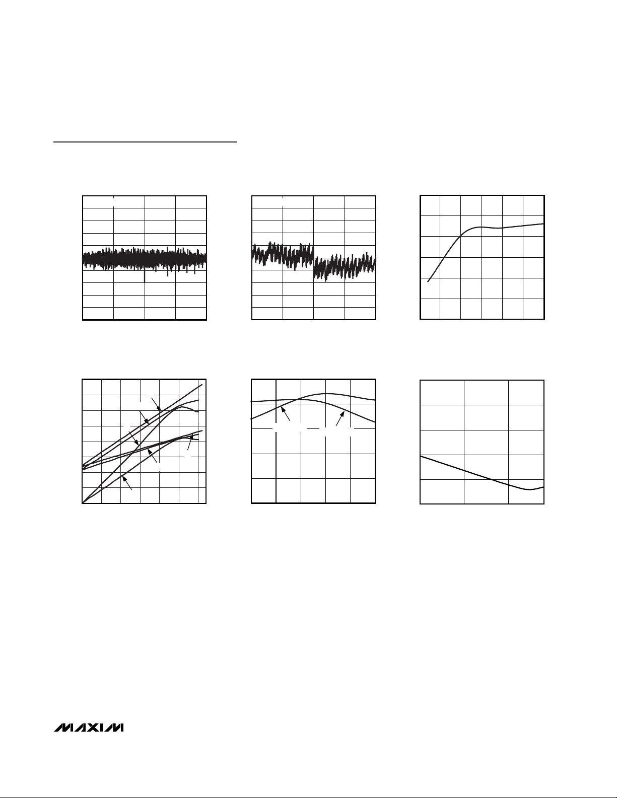
Typical Operating Characteristics (continued)
(AVDD= 5.0V, V
REFADC
= V
REFDAC
= 2.5V for DVDD= 3.0V; TA= +25°C, unless otherwise noted.)
(V)
V
A: T
= -40°C, AVDD = 5V, DVDD = 3V
A
= -40°C, AVDD = 3V, DVDD = 2V
B: T
A
= +25°C, AVDD = 5V, DVDD = 3V
C: T
A
ADC REFERENCE VOLTAGE (1.25V)
vs. LOAD CURRENT
1.2520
1.2515
1.2510
1.2505
1.2500
REFADC
1.2495
1.2490
1.2485
1.2480
-100 500
A
B
C
D
E
F
(µA)
I
REFADC
= +25°C, AVDD = 3V, DVDD = 2V
D: T
A
= +85°C, AVDD = 5V, DVDD = 3V
E: T
A
= +85°C, AVDD = 3V, DVDD = 2V
F: T
A
ADC REFERENCE VOLTAGE (2.5V)
vs. LOAD CURRENT
2.510
2.508
2.506
2.504
(V)
V
REFADC
2.502
2.500
2.498
2.496
2.494
2.492
2.490
A
B
E
F
I
REFADC
C
D
(µA)
ADC REFERENCE VOLTAGE (2.048V)
vs. LOAD CURRENT
A
B
E
F
C
D
I
(µA)
REFADC
= +25°C, AVDD = 3V, DVDD = 2V
D: T
A
= +85°C, AVDD = 5V, DVDD = 3V
E: T
A
= +85°C, AVDD = 3V, DVDD = 2V
F: T
A
MAX1329 toc21
4003000 100 200
4003000 100 200
4003000 100 200-100 500
MAX1329 toc20
MAX1329 toc22
2.056
2.054
2.052
2.050
(V)
2.048
REFADC
V
2.046
2.044
2.042
2.040
-100 500
A: TA = -40°C, AVDD = 5V, DVDD = 3V
= -40°C, AVDD = 3V, DVDD = 2V
B: T
A
= +25°C, AVDD = 5V, DVDD = 3V
C: T
A
A: TA = -40°C, AVDD = 5V, DVDD = 3V
B: T
C: T
= +25°C, AVDD = 3V, DVDD = 2V
D: T
= -40°C, AVDD = 3V, DVDD = 2V
A
= +25°C, AVDD = 5V, DVDD = 3V
A
A
= +85°C, AVDD = 5V, DVDD = 3V
E: T
A
= +85°C, AVDD = 3V, DVDD = 2V
F: T
A
Page 16
MAX1329/MAX1330
12-/16-Bit DASs with ADC, DACs, DPIOs, APIOs,
Reference, Voltage Monitors, and Temp Sensor
16 ______________________________________________________________________________________
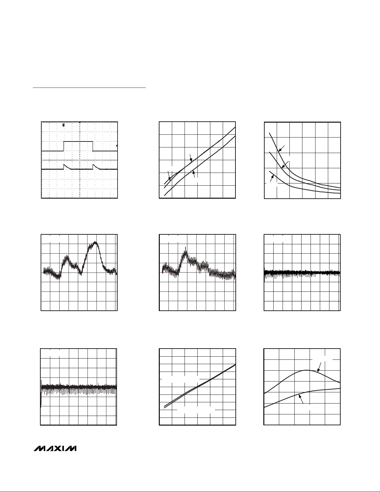
Typical Operating Characteristics (continued)
(AVDD= 5.0V, V
REFADC
= V
REFDAC
= 2.5V for DVDD= 3.0V; TA= +25°C, unless otherwise noted.)
1ms/div
ADC REFERENCE LINE TRANSIENT
(V
ADCREF
= +2.048V)
AV
DD
V
ADCREF
2.048V
3V
10mV/div
500mV/div
MAX1329 toc27
1ms/div
ADC REFERENCE LINE TRANSIENT
(V
ADCREF
= +2.5V)
AV
DD
V
ADCREF
2.5V
3V
10mV/div
500mV/div
MAX1329 toc28
ADC REFERENCE VOLTAGE (2.048V)
vs. ANALOG SUPPLY VOLTAGE
2.055
2.054
2.053
2.052
2.051
2.050
(V)
2.049
2.048
REFADC
2.047
V
2.046
2.045
2.044
2.043
2.042
2.041
TA = -40°C
TA = +25°C
TA = +85°C
AVDD SUPPLY VOLTAGE (V)
ADC REFERENCE VOLTAGE (2.5V)
vs. ANALOG SUPPLY VOLTAGE
2.510
2.508
5.04.53.0 3.5 4.02.5 5.5
MAX1329 toc24
2.506
2.504
2.502
(V)
2.500
REFADC
V
2.498
2.496
2.494
2.492
2.490
TA = -40°C
TA = +25°C
TA = +85°C
AVDD SUPPLY VOLTAGE (V)
5.04.53.0 3.5 4.02.5 5.5
MAX1329 toc25
V
AV
ADCREF
ADC REFERENCE LINE TRANSIENT
(V
= +1.25V)
ADCREF
DD
1ms/div
MAX1329 toc26
500mV/div
3V
10mV/div
1.25V
ADC REFERENCE LINE TRANSIENT
(V
= +1.25V)
ADCREF
AV
DD
V
ADCREF 1.25V
1ms/div
MAX1329 toc29
500mV/div
5V
20mV/div
V
ADCREF
ADC REFERENCE LINE TRANSIENT
= +2.048V)
(V
ADCREF
AV
DD
1ms/div
MAX1329 toc30
500mV/div
5V
20mV/div
2.048V
Page 17
MAX1329/MAX1330
12-/16-Bit DASs with ADC, DACs, DPIOs, APIOs,
Reference, Voltage Monitors, and Temp Sensor
______________________________________________________________________________________ 17
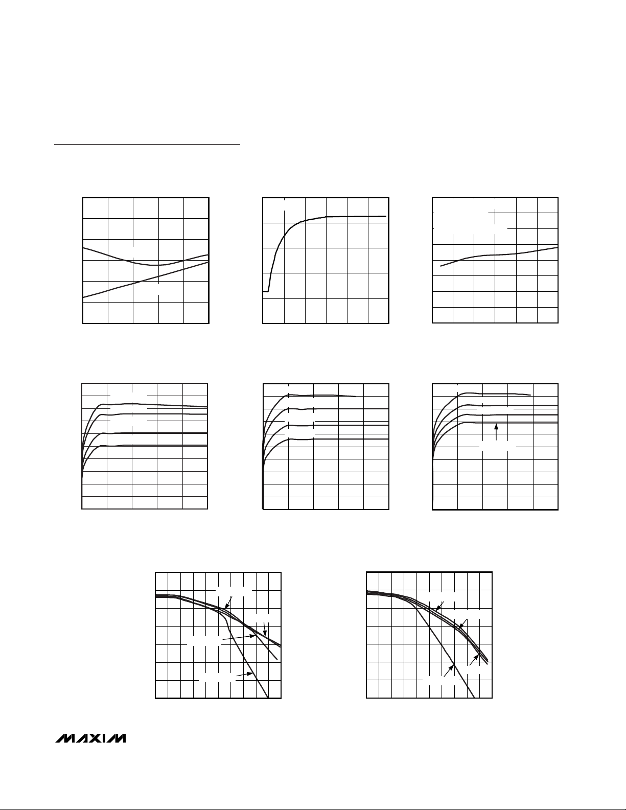
Typical Operating Characteristics (continued)
(AVDD= 5.0V, V
REFADC
= V
REFDAC
= 2.5V for DVDD= 3.0V; TA= +25°C, unless otherwise noted.)
DAC SUPPLY CURRENT
vs. ANALOG SUPPLY VOLTAGE
MAX1329 toc38
AVDD (V)
I
AVDD
(µA)
5.04.54.03.53.0
35
40
45
50
55
60
65
70
75
80
30
2.5 5.5
V
REFDAC
= 2.5V, DACB
V
REFDAC
= 2.5V, DACA
1.20
1.60
1.40
2.00
1.80
2.40
2.20
2.60
-40 10-15 35 60 85
DAC OFFSET VOLTAGE
vs. TEMPERATURE
MAX1329 toc39
TEMPERATURE (°C)
OFFSET (mV)
AVDD = 5.5V
AVDD = 2.7V
ADC REFERENCE LINE TRANSIENT
= +2.5V)
(V
ADCREF
AV
DD
V
ADCREF
1ms/div
DAC INTEGRAL NONLINEARITY
vs. DIGITAL INPUT CODE (AV
2.0
V
= 2.5V
REFDAC
1.5
1.0
0.5
0
INL (LSB)
-0.5
-1.0
-1.5
-2.0
0 1000 1500 2000500 2500 3000 3500 4000
DIGITAL INPUT CODE
MAX1329 toc31
= 3V)
DD
ADC REFERENCE SUPPLY CURRENT
vs. ANALOG SUPPLY VOLTAGE
446
500mV/div
5V
20mV/div
2.5V
MAX1329 toc34
445
444
(µA)
443
AVDD
I
2.048V
442
441
440
2.5 5.5
2.5V
1.25V
AVDD SUPPLY VOLTAGE (V)
DAC INTEGRAL NONLINEARITY
vs. DIGITAL INPUT CODE (AV
2.0
V
= 2.5V
REFDAC
1.5
1.0
0.5
0
INL (LSB)
-0.5
-1.0
-1.5
-2.0
0 1000 1500 2000500 2500 3000 3500 4000
DIGITAL INPUT CODE
DD
5.04.54.03.53.0
= 5V)
MAX1329 toc32
TURN-ON TIME (ms)
MAX1329 toc35
DNL (LSB)
2.0
1.5
1.0
0.5
-0.5
-1.0
-1.5
-2.0
ADC REFERENCE TURN-ON TIME
vs. ANALOG SUPPLY VOLTAGE
10
8
6
4
2
0
2.5 5.5
2.5V
2.048V
1.25V
5.04.54.03.53.0
AVDD SUPPLY VOLTAGE (V)
DAC DIFFERENTIAL NONLINEARITY
vs. DIGITAL INPUT CODE (AV
V
= 2.5V
REFDAC
0
0 1000 1500 2000500 2500 3000 3500 4000
DIGITAL INPUT CODE
DD
= 3V)
MAX1329 toc33
MAX1329 toc36
DAC DIFFERENTIAL NONLINEARITY
vs. DIGITAL INPUT CODE (AV
2.0
V
= 2.5V
REFDAC
1.5
1.0
0.5
0
DNL (LSB)
-0.5
-1.0
-1.5
-2.0
0 1000 1500 2000500 2500 3000 3500 4000
DIGITAL INPUT CODE
= 5V)
DD
MAX1329 toc37
Page 18
MAX1329/MAX1330
12-/16-Bit DASs with ADC, DACs, DPIOs, APIOs,
Reference, Voltage Monitors, and Temp Sensor
18 ______________________________________________________________________________________
Typical Operating Characteristics (continued)
(AVDD= 5.0V, V
REFADC
= V
REFDAC
= 2.5V for DVDD= 3.0V; TA= +25°C, unless otherwise noted.)
OP-AMP INPUT OFFSET VOLTAGE
vs. COMMON-MODE VOLTAGE
MAX1329 toc46
VCM (V)
V
OS
(mV)
4.54.03.0 3.51.0 1.5 2.0 2.50.5
1
2
3
4
5
6
7
8
9
10
0
0 5.0
AVDD = 3V
AVDD = 5V
-1.000
-0.975
-0.950
-0.925
-0.900
-0.875
-0.850
-0.825
-0.800
-40 -15 10 35 60 85
DAC GAIN ERROR
vs. TEMPERATURE
MAX1329 toc40
TEMPERATURE (°C)
ERROR (%)
AVDD = 5.5V
AVDD = 2.7V
4µs/div
DAC SLEW RATE/CROSSTALK TRANSIENT
RESPONSE (V
REFDAC
= +1.25V)
V
OUTA
V
OUTB
1mV/div
1V/div
1.25V
MAX1329 toc41
AVDD = +5.0V
4µs/div
DAC SLEW RATE/CROSSTALK TRANSIENT
RESPONSE (V
REFDAC
= +2.048V)
V
OUTA
V
OUTB
1mV/div
1V/div
2.048V
MAX1329 toc42
AVDD = +5.0V
4µs/div
DAC SLEW RATE/CROSSTALK TRANSIENT
RESPONSE (V
REFDAC
= +2.5V)
V
OUTA
V
OUTB
1mV/div
1V/div
2.5V
0V
MAX1329 toc43
AVDD = +5.0V
200ns/div
DAC DIGITAL FEEDTHROUGH TRANSIENT
RESPONSE (V
REFDAC
= +2.50V)
V
SCLK
V
OUTA
20mV/div
2V/div
MAX1329 toc44
AVDD = +5.0V
OP-AMP INPUT OFFSET VOLTAGE
vs. TEMPERATURE
10
VCM = AVDD/2
9
8
AVDD = 5V
7
6
(mV)
5
OS
V
4
AVDD = 3V
3
2
1
0
-40 85
TEMPERATURE (°C)
MAX1329 toc45
603510-15
Page 19
MAX1329/MAX1330
12-/16-Bit DASs with ADC, DACs, DPIOs, APIOs,
Reference, Voltage Monitors, and Temp Sensor
______________________________________________________________________________________ 19
Typical Operating Characteristics (continued)
(AVDD= 5.0V, V
REFADC
= V
REFDAC
= 2.5V for DVDD= 3.0V; TA= +25°C, unless otherwise noted.)
OP-AMP SUPPLY CURRENT
vs. ANALOG SUPPLY VOLTAGE
MAX1329 toc47
AVDD (V)
I
AVDD
(µA)
5.04.54.03.53.0
55
60
65
70
75
80
85
90
95
100
50
2.5 5.5
A: = RL = 5kΩ, AVDD = 5V, DVDD = 3V
C: = R
E: = R
OP-AMP MAXIMUM OUTPUT VOLTAGE
vs. TEMPERATURE
50
RL TO AVDD/2
40
(mA)
30
OUT
- V
DD
20
AV
10
0
-40 85
= 10kΩ, AVDD = 5V, DVDD = 3V
L
= 100kΩ, AVDD = 5V, DVDD = 3V
L
A
C
E
TEMPERATURE (°C)
B: = R
D: = R
F: = R
B
3510-15
L
L
L
OP-AMP OUTPUT IMPEDANCE
vs. FREQUENCY
50
0
0101 100 1000
FREQUENCY (kHz)
C
D
F
603510-15-40 85
= 5kΩ, AVDD = 3V, DVDD = 2V
B: = R
L
= 10kΩ, AVDD = 3V, DVDD = 2V
D: = R
L
= 100kΩ, AVDD = 3V, DVDD = 2V
F: = R
L
80
70
AVDD = 3.0V
60
50
PSRR (dB)
40
30
20
MAX1329 toc50
D
F
60
= 5kΩ, AVDD = 3V, DVDD = 2V
= 10kΩ, AVDD = 3V, DVDD = 2V
= 100kΩ, AVDD = 3V, DVDD = 2V
OP-AMP PSRR
vs. FREQUENCY
AVDD = 5.0V
FREQUENCY (kHz)
MAX1329 toc48
10 100
10000.01 0.1 1
OP-AMP MAXIMUM OUTPUT VOLTAGE
140
TO AVDD/2
R
RL TO AVDD/2
L
120
100
(mA)
80
OUT
- V
60
DD
AV
40
20
0
A: = RL = 5kΩ, AVDD = 5V, DVDD = 3V
= 10kΩ, AVDD = 5V, DVDD = 3V
C: = R
L
= 100kΩ, AVDD = 5V, DVDD = 3V
E: = R
L
A
B
500
450
400
350
300
250
200
IMPEDANCE (Ω)
150
100
vs. TEMPERATURE
E
TEMPERATURE (°C)
MAX1329 toc49
MAX1329 toc51
Page 20
MAX1329/MAX1330
12-/16-Bit DASs with ADC, DACs, DPIOs, APIOs,
Reference, Voltage Monitors, and Temp Sensor
20 ______________________________________________________________________________________
Typical Operating Characteristics (continued)
(AVDD= 5.0V, V
REFADC
= V
REFDAC
= 2.5V for DVDD= 3.0V; TA= +25°C, unless otherwise noted.)
OP-AMP GAIN AND PHASE
vs. FREQUENCY
MAX1329 toc52
FREQUENCY (kHz)
GAIN/PHASE (dB/deg)
10 100
-60
-90
-120
-150
60
30
0
-30
-180
10000.1 1
AVDD = 5V, 3V
C
L
= 0pF, 220pF
AVDD = 5V
C
L
= 0pF
AVDD = 3V
C
L
= 0pF
AVDD = 3V
C
L
= 220pF
AVDD = 3V
C
L
= 220pF
GAIN
PHASE
MAX1329 toc53
COM VOLTAGE (V)
R
ON
(Ω)
2.52.01.51.00.5
95
100
105
110
115
120
125
130
135
140
90
0 3.0
ANALOG SWITCH ON-RESISTANCE
vs. COM VOLTAGE (AV
DD
= 3V)
TA = +85°C
TA = +25°C
TA = -40°C
ANALOG SWITCH ON-RESISTANCE
vs. COM VOLTAGE (AV
DD
= 5V)
MAX1329 toc54
COM VOLTAGE (V)
R
ON
(Ω)
542 3
85
90
95
100
110
105
115
120
80
16
TA = +85°C
TA = +25°C
TA = -40°C
ANALOG SWITCH TURN-ON/-OFF TIME
vs. ANALOG SUPPLY VOLTAGE
MAX1329 toc55
AVDD (V)
t
ON
/t
OFF
(ns)
5.04.54.03.53.0
10
20
30
40
50
60
70
0
2.5 5.5
tON, DVDD = 3V
tON, DVDD = 2V
t
OFF
, DVDD = 2V
t
OFF
, DVDD = 3V
RL = 1kΩ
ANALOG SWITCH TURN-ON/-OFF TIME
vs. TEMPERATURE
MAX1329 toc56
TEMPERATURE (°C)
t
ON/
t
OFF
(ns)
6035-15 10
10
20
30
40
60
50
70
80
0
-40 85
tON, AVDD = 5V
tON, AVDD = 3V
t
OFF
, AVDD = 3V
t
OFF
, AVDD = 5V
R
L
= 1kΩ
ANALOG SWITCH LEAKAGE CURRENT
vs. TEMPERATURE
MAX1329 toc57
TEMPERATURE (°C)
I
LEAKAGE
(pA)
603510-15
20
40
60
80
100
120
140
160
180
200
0
-40 85
OFF LEAKAGE
ON LEAKAGE
ANALOG SWITCH ON-RESPONSE
vs. FREQUENCY
MAX1329 toc58
FREQUENCY (kHz)
GAIN (dB)
110
-2
4
2
0
-4
-6
-8
-10
1000 0.1
AVDD = 5V
AVDD = 3V
ANALOG SWITCH CROSSTALK AND OFF
ISOLATION vs. FREQUENCY (AV
DD
= 3V)
MAX1329 toc59
FREQUENCY (kHz)
OFF ISOLATION (dB)
100 1000
-80
-90
-100
-110
-120
-40
-50
-60
-70
-130
10,0000.1 1 10
OFF ISOLATION
CROSSTALK
ANALOG SWITCH CROSSTALK AND OFF
ISOLATION vs. FREQUENCY (AV
DD
= 5V)
MAX1329 toc60
FREQUENCY (kHz)
OFF ISOLATION (dB)
100 1000
-80
-90
-100
-110
-120
-40
-50
-60
-70
-130
10,0000.1 1 10
OFF ISOLATION
CROSSTALK
Page 21
MAX1329/MAX1330
12-/16-Bit DASs with ADC, DACs, DPIOs, APIOs,
Reference, Voltage Monitors, and Temp Sensor
______________________________________________________________________________________ 21
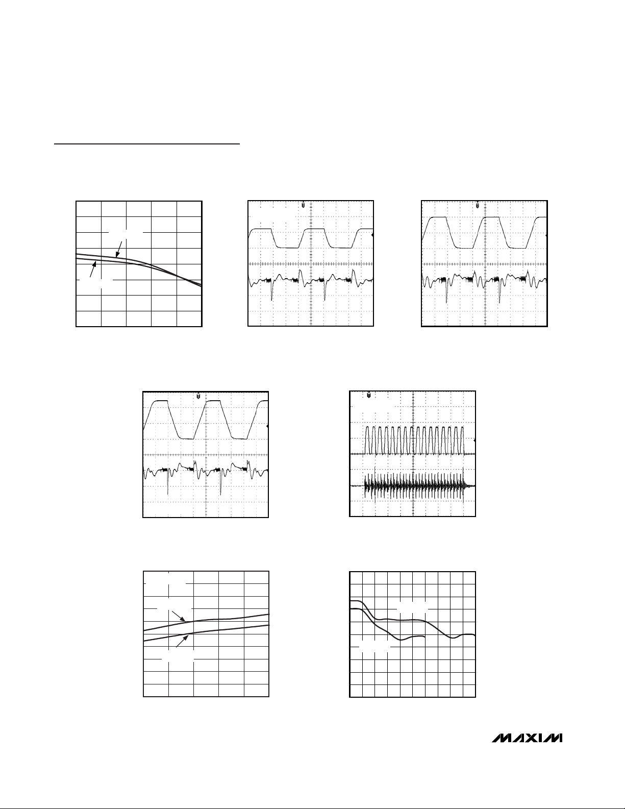
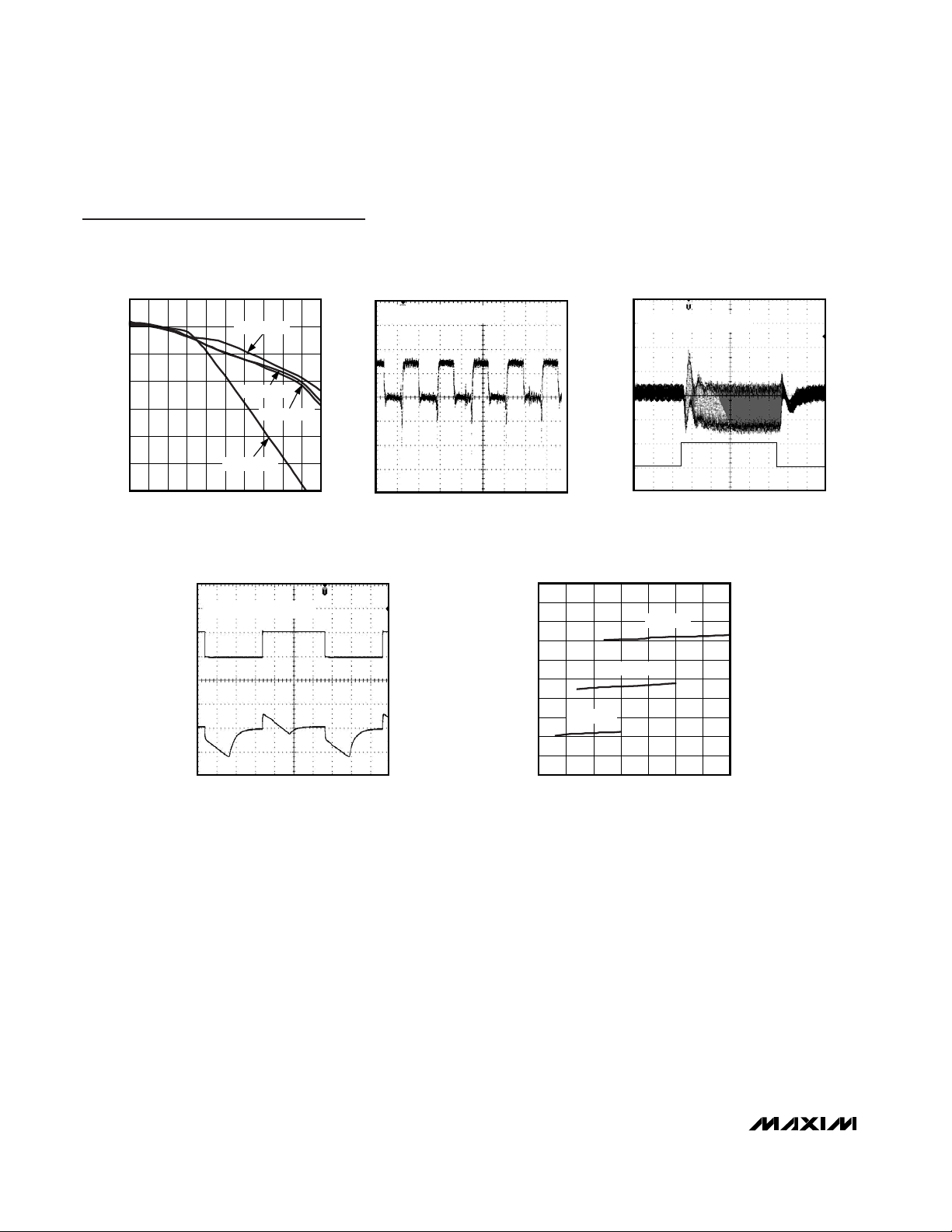
Typical Operating Characteristics (continued)
(AVDD= 5.0V, V
REFADC
= V
REFDAC
= 2.5V for DVDD= 3.0V; TA= +25°C, unless otherwise noted.)
TEMPERATURE-SENSOR ACCURACY
vs. TEMPERATURE
MAX1329 toc61
TEMPERATURE (°C)
ERROR (°C)
603510-15
-1.0
-0.5
0
0.5
1.0
1.5
-1.5
-40 85
INTERNAL
EXTERNAL
CHARGE-PUMP EFFICIENCY
vs. OUTPUT CURRENT (AV
DD
= 4V)
MAX1329 toc65
I
OUT
(mA)
EFFICIENCY (%)
2015105
10
20
30
40
50
60
70
80
90
100
0
0
25
DVDD = 2.2V
DVDD = 2.5V
DV
DD
= 3.0V
DV
DD
= 3.6V
CHARGE-PUMP EFFICIENCY
vs. OUTPUT CURRENT (AV
DD
= 5V)
MAX1329 toc66
I
OUT
(mA)
EFFICIENCY (%)
2015105
10
20
30
40
50
60
70
80
90
100
0
025
DVDD = 2.7V
DVDD = 3.3V
DVDD = 3.6V
DV
DD
=3.0V
CHARGE-PUMP OUTPUT VOLTAGE
vs. OUTPUT CURRENT (AV
DD
= 3V)
MAX1329 toc67
I
OUT
(mA)
AV
DD
(V)
45403530252015105
2.6
2.7
2.8
2.9
3.0
3.1
3.2
2.5
050
DVDD = 1.8V
DVDD = 2.0V
DVDD = 3.0V
DV
DD
= 2.5V
MAX1329 toc68
I
OUT
(mA)
AV
DD
(V)
45403530252015105
3.6
3.7
3.8
3.9
4.0
4.1
4.2
3.5
050
CHARGE-PUMP OUTPUT VOLTAGE
vs. OUTPUT CURRENT (AV
DD
= 4V)
DVDD = 2.5V
DV
DD
= 2.2V
DVDD = 3.6V
DVDD = 3.0V
CHARGE-PUMP EFFICIENCY
vs. OUTPUT CURRENT (AVDD = 3V)
100
90
80
70
60
50
40
EFFICIENCY (%)
30
20
10
0
025
DVDD = 1.8V
DV
DVDD = 2.5V
DVDD = 3.0V
DD
= 2.0V
I
OUT
(mA)
2015105
TEMPERATURE-SENSOR THERMAL
STEP RESPONSE (+25°C TO +85°C)
100
τ = 11s
80
60
40
TEMPERATURE (°C)
20
0
-5 3515 55 75 95 115
MAX1329 toc64
TIME (s)
INTERNAL TEMPERATURE-SENSOR SUPPLY
CURRENT vs. SUPPLY VOLTAGE
120
INTERNAL 2.5V REFERENCE
CLKIO = 3.6864MHz
115
MAX1329 toc62
ADC CLOCK DIV = 1
CONVERSION RATE = 4ksps
110
105
(µA)
100
AVDD
I
95
90
85
80
2.5 3.53.0 4.0 4.5 5.0 5.5
AVDD (V)
MAX1329 toc63
Page 22
MAX1329/MAX1330
12-/16-Bit DASs with ADC, DACs, DPIOs, APIOs,
Reference, Voltage Monitors, and Temp Sensor
22 ______________________________________________________________________________________
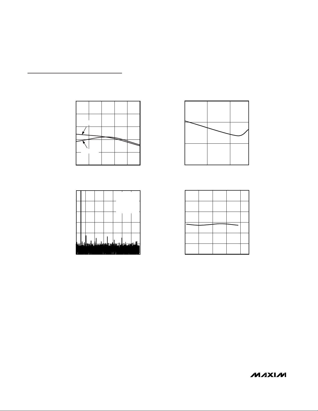
Typical Operating Characteristics (continued)
(AVDD= 5.0V, V
REFADC
= V
REFDAC
= 2.5V for DVDD= 3.0V; TA= +25°C, unless otherwise noted.)
CHARGE-PUMP OUTPUT VOLTAGE
vs. OUTPUT CURRENT (AV
DD
= 5V)
MAX1329 toc69
I
OUT
(mA)
AV
DD
(V)
45403530252015105
4.6
4.7
4.8
4.9
5.0
5.1
5.2
4.5
050
DVDD = 2.7V
DVDD = 3.3V
DV
DD
= 3.0V
DVDD = 3.6V
200
260
240
220
300
280
380
360
340
320
400
1.5 2.0 2.5 3.0 3.5 4.0 4.5 5.0
CHARGE-PUMP SUPPLY CURRENT
vs. SUPPLY VOLTAGE
MAX1329 toc73
DVDD (V)
I
DVDD
(µA)
AVDD = 3.0V
AVDD = 4.0V
AVDD = 5V
2ms/div
CHARGE-PUMP LINE TRANSIENT RESPONSE
FOR +2.0V TO +2.5V STEP INPUT
AV
DD
DV
DD
2.5V
2V
100mV/div
500mV/div
MAX1329 toc72
AV
DD
= +3.0V, 3.0kΩ LOAD
4µs/div
CHARGE-PUMP RIPPLE (I
OUT
= 5mA,
DV
DD
= 2V, CHARGE-PUMP CLOCK = 78kHz)
AV
DD
2mV/div
MAX1329 toc70
AVDD = +3.0V, DVDD = +2.0V
1ms/div
CHARGE-PUMP LOAD TRANSIENT
RESPONSE FOR 0.1mA TO 1.0mA LOAD
AV
DD
I
AVDD
1mA
0
1mV/div
MAX1329 toc71
AV
DD
= +3.0V, DVDD = +2.0V
Page 23

MAX1329/MAX1330
12-/16-Bit DASs with ADC, DACs, DPIOs, APIOs,
Reference, Voltage Monitors, and Temp Sensor
______________________________________________________________________________________ 23
Pin Description
PIN
MAX1329 MAX1330
1 1 DPIO1 Digital Programmable Input/Output 1
2 2 DPIO2 Digital Programmable Input/Output 2
3 3 DPIO3 Digital Programmable Input/Output 3
4 4 DPIO4 Digital Programmable Input/Output 4
5 5 DOUT
6 6 SCLK
77DIN
88CS
99RST1
10 10 RST2
11 11 APIO1 Analog Programmable Input/Output 1
12 12 APIO2 Analog Programmable Input/Output 2
13 13 APIO3 Analog Programmable Input/Output 3
14 14 APIO4 Analog Programmable Input/Output 4
15 15 SNO1 Analog Switch 1 Normally-Open Terminal
16 16 SCM1 Analog Switch 1 Common Terminal
17 17 SNC1 Analog Switch 1 Normally-Closed Terminal
18 18 IN1+ Operational Amplifier 1 Noninverting Input
19 19 IN1- Operational Amplifier 1 Inverting Input. Also internally connected to ADC mux.
20 20 OUT1 Operational Amplifier 1 Output. Also internally connected to ADC mux.
21 — N.C. No Connection. Not internally connected.
22 — FBB DACB Force-Sense Feedback Input. Also internally connected to ADC mux.
23 — OUTB DACB Force-Sense Output. Also internally connected to ADC mux.
— 21 IN2+ Operational Amplifier 2 Noninverting Input
— 22 IN2- Operational Amplifier 2 Inverting Input. Also internally connected to ADC mux.
— 23 OUT2 Operational Amplifier 2 Output. Also internally connected to ADC mux.
NAME FUNCTION
Serial-Data Output. DOUT outputs serial data from the data register. DOUT changes on the
falling edge of SCLK and is valid on the rising edge of SCLK. When CS is high, DOUT is
high impedance, unless APIO1 is programmed for SPI mode.
Serial-Clock Input. Apply an external serial clock to transfer data to and from the device.
When CS is high, SCLK is inactive unless APIO3 is configured for SPI mode. Then the input
on SCLK is level-shifted and output at APIO3.
Serial-Data Input. Data on DIN is clocked in on the rising edge of SCLK when CS is low.
When CS is high, DIN is inactive unless APIO2 is configured for SPI mode. Then the input
on DIN is level-shifted and output at APIO2.
Active-Low Chip-Select Input. Drive CS low to transfer data to and from the device. When
CS is high and APIO4 is configured for SPI mode, APIO4 is low.
Open-Drain Reset Output 1. RST1 remains low while DV
reprogrammed as a push-pull, active-high, or active-low Status register interrupt output.
Open-Drain Reset Output 2. RST2 remains low while DV
reprogrammed as a push-pull, active-high, or active-low Status register interrupt output.
DD
DD
is below 1.8V. RST1 can be
is below 2.7V. RST2 can be
Page 24
MAX1329/MAX1330
12-/16-Bit DASs with ADC, DACs, DPIOs, APIOs,
Reference, Voltage Monitors, and Temp Sensor
24 ______________________________________________________________________________________
Pin Description (continued)
PIN
MAX1329 MAX1330
24 24 OUTA DACA Force-Sense Output. Also internally connected to ADC mux.
25 25 FBA DACA Force-Sense Feedback Input. Also internally connected to ADC mux.
26 26 REFDAC
27 27 SNC2 Analog Switch 2 Normally-Closed Terminal
28 28 SCM2 Analog Switch 2 Common Terminal
29 29 SNO2 Analog Switch 2 Normally-Open Terminal
30 30 AIN2 Analog Input 2. Also internally connected to ADC mux.
31 31 AIN1 Analog Input 1. Also internally connected to ADC mux.
32 32 REFADC
33 33 REFADJ
34 34 AGND Analog Ground
35 35 AV
36 36 C1B
37 37 C1A
38 38 DV
39 39 DGND Digital Ground
40 40 CLKIO
——EP
NAME FUNCTION
DAC Internal Reference Buffer Output/DAC External Reference Input. In internal reference
mode, REFDAC provides a 1.25V, 2.048V, or 2.5V internal reference buffer output. In
external DAC reference buffer mode, disable internal reference buffer. Bypass REFDAC to
AGND with a 1µF capacitor.
ADC Internal Reference Buffer Output/ADC External Reference Input. In internal reference
mode, REFADC provides a 1.25V, 2.048V, or 2.5V internal reference buffer output. In
external ADC reference buffer mode, disable internal reference buffer. Bypass REFADC to
AGND with a 1µF capacitor.
Internal Reference Output/Reference Buffer Amplifiers Input. In internal reference mode,
bypass REFADJ to AGND with a 0.01µF capacitor. In external reference mode, disable
internal reference.
Analog Supply Input. Bypass AVDD to AGND with at least a 0.01µF capacitor. With the
DD
charge pump enabled, see Table 32 for required capacitor values.
Charge-Pump Capacitor Input B. Connect C
required capacitor values.
Charge-Pump Capacitor Input A. Connect C
required capacitor values.
Digital Supply Input. Bypass DVDD to DGND with at least a 0.01µF capacitor. When using
DD
charge pump, see Table 32 for required capacitor values.
Clock Input/Output. In internal clock mode, enable CLKIO output for external use. In
external clock mode, apply a clock signal at CLKIO for the ADC and charge pump.
Exposed Pad. The exposed pad is located on the package bottom and is internally
connected to AGND. Connect EP to the analog ground plane. Do not route any PCB traces
under the package.
across C1A and C1B. See Table 32 for
FLY
across C1A and C1B. See Table 32 for
FLY
Page 25
Detailed Description
The MAX1329/MAX1330 smart DASs are based on a
312ksps, 12-bit SAR ADC with a 1ksps, 16-bit DSP
mode. The ADC includes a differential multiplexer, a programmable gain amplifier (PGA) with gains of 1, 2, 4,
and 8, a 20-bit accumulator, internal dither, a 16-word
FIFO, and an alarm register. The MAX1329/MAX1330
operate with a digital supply down to 1.8V and feature an
internal charge pump to boost the supply voltage for the
analog circuitry that requires 2.7V to 5.5V.
The MAX1329/MAX1330 include an internal reference
with programmable buffer for the ADC, two analog external inputs as well as inputs from other internal circuitry,
an internal/external temperature sensor, internal oscillator, dual single-pole, double-throw (SPDT) switches, four
digital programmable I/Os, four analog programmable
I/Os, and dual programmable voltage monitors.
The MAX1329 features dual 12-bit force-sense DACs
with programmable reference buffer and one operational amplifier. The MAX1330 includes one 12-bit forcesense DAC with programmable reference buffer and
dual op amps. DACA can be sequenced with a 16-word
FIFO. The DAC buffers and op amps have internal analog switches between the output and the inverting input.
Power-On Reset
After a power-on reset, the DVDDvoltage supervisor is
enabled with thresholds at 1.8V and 2.7V. All digital
and analog programmable I/Os (DPIOs and APIOs) are
configured as inputs with pullups enabled. The internal
oscillator is enabled and is output at CLKIO once the
1.8V reset trip threshold has been exceeded and the
subsequent timeout period has expired. See the
Register Bit Descriptions
section for the default values
after a power-on reset.
Power-On Setup
After applying power to AVDD:
1) Write to the Reset register. This initializes the temperature sensor and voltage reference trim logic.
2) Within 3ms following the reset, configure the charge
pump as desired by writing to the CP/VM Control
register. The details of programming the charge
pump are described in the
Charge Pump
section.
Charge Pump
Power AVDDand DVDDby any one of the following
ways: drive AVDDand DVDDwith a single external
power supply, drive AVDDand DVDDwith separate
external power supplies, or drive DVDDwith an external
supply and enable the internal charge pump to generate AVDDor short DVDDto AVDDinternally.
MAX1329/MAX1330
12-/16-Bit DASs with ADC, DACs, DPIOs, APIOs,
Reference, Voltage Monitors, and Temp Sensor
______________________________________________________________________________________ 25
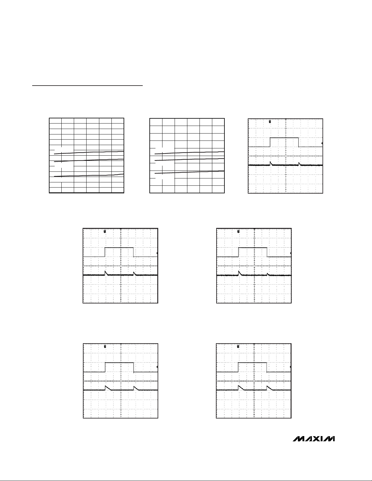
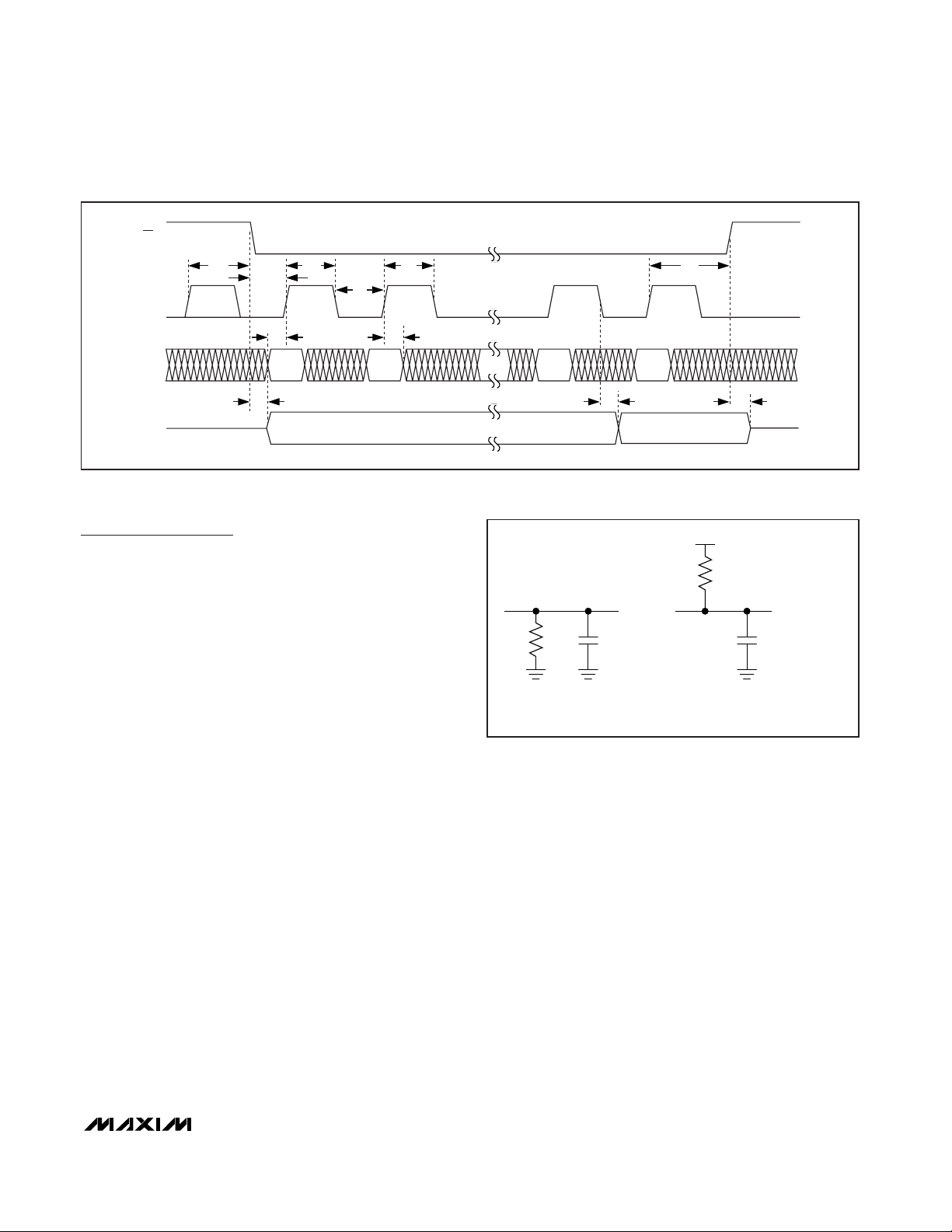
Figure 1. Detailed Serial-Interface Timing Diagram
Figure 2. DOUT Enable and Disable Time Load Circuits
CS
SCLK
DIN
DOUT
t
CSH
t
CYC
t
CSS
t
t
DV
t
DS
t
CH
CL
t
DH
t
CSH
DOUT
3kΩ
a) FOR ENABLE, HIGH IMPEDANCE
AND VOL TO VOH.
TO V
OH
FOR DISABLE, V
C
= 20pF
LOAD
TO HIGH IMPEDANCE.
OH
t
DO
DV
DD
3kΩ
DOUT
C
= 20pF
LOAD
b) FOR ENABLE, HIGH IMPEDANCE
AND VOH TO VOL.
TO V
OL
FOR DISABLE, V
t
TR
TO HIGH IMPEDANCE.
OL
Page 26
MAX1329/MAX1330
12-/16-Bit DASs with ADC, DACs, DPIOs, APIOs,
Reference, Voltage Monitors, and Temp Sensor
26 ______________________________________________________________________________________
Upon a power-on reset, the charge pump is disabled.
Enable the charge pump through the CP/VM Control
register. When the charge pump is in its off state, AV
DD
is isolated from DVDDunless the bypass switch is
enabled. To bypass the charge pump and directly connect DVDDto AVDD, enable (close) the bypass switch
through the CP/VM Control register (see Tables 21 and
22). During the on mode, the charge pump boosts
DVDDand regulates the voltage to generate the selected output voltage at AVDD. The charge-pump output
voltage selections are 3.0V, 4.0V, or 5.0V.
The charge-pump clock and ADC clock are synchronized from the same master clock. The charge pump
uses a pulse-width-modulation (PWM) scheme to regulate the output voltage. The charge pump supports a
maximum load of 25mA of current to an external device
including what is required for internal circuitry.
Power Modes
Three power modes are available for the MAX1329/
MAX1330: shutdown, sleep, and normal operation. In shutdown mode, all functional blocks are powered down except
the serial interface, data registers, and wake-up circuitry (if
enabled). Sleep mode is identical to shutdown mode
except the DV
DD
voltage monitors (if enabled) remain
active. Global sleep or shutdown mode is initiated through a
DPIO configured as SLP or SHDN inputs. In normal mode,
each analog and digital block can be powered up or shut
down individually through its respective control register.
Voltage Supervisors
The MAX1329/MAX1330 provide two programmable voltage supervisors, one for DVDDand one for AVDD. The
DVDDvoltage supervisor has two thresholds (set to 1.8V
and 2.7V by default) that are both enabled after a poweron reset. On initial power-up, RST1 is assigned the 1.8V
monitor output and RST2 is assigned the 2.7V monitor
output, both for DVDD. If DVDDfalls below the 1.8V or
2.7V threshold, the VM1A bit or VM1B bit, respectively, in
the Status register is set. The VM1A and VM1B status
bits can also be mapped to the interrupt generator.
The default states of RST1 and RST2 are open-drain
outputs but can be programmed as push-pull Status
register interrupts through the CP/VM Control register.
The AV
DD
voltage supervisor provides three programmable thresholds. If AVDDfalls below the programmed
threshold, the VM2 bit is set in the Status register. The
VM2 status bit can also be mapped to the interrupt
generator.
Interrupt Generator
The interrupt generator accepts inputs from other internal
circuits to provide an interrupt to an external microcontroller
(µC). The sources for generating an interrupt are programmable through the serial interface. Possible sources
include a rising or falling edge on the digital and analog
programmable inputs, ADC alarms, an ADC conversion
complete, an ADC FIFO full, an ADC accumulator full, and
the voltage-supervisor outputs. The interrupt causes RST1
and/or RST2 to assert when configured as an interrupt out-
put. The interrupt remains asserted until the Status register
is read. See the CP/VM Control register for programming
the RST1 and RST2 outputs as interrupts and the Interrupt
Mask register for programming the interrupt sources.
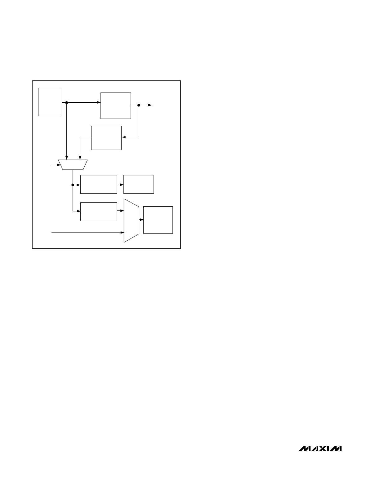
Internal Oscillator and Programmable
Clock Dividers
The MAX1329/MAX1330 feature an internal oscillator,
which operates at a fixed frequency of 3.6864MHz. When
enabled, the internal oscillator provides the master clock
source for the ADC and charge pump. To allow external
devices to use the internally generated clock, configure
CLKIO as an output through the Clock Control register.
The CLKIO output frequency is configurable for
0.9216MHz, 1.8432MHz, and 3.6864MHz. When the internal oscillator is enabled, and regardless of the CLKIO output frequency, the ADC and charge-pump clock dividers
always receive a 3.6864MHz clock signal (see Figure 3).
After a power-on reset, CLKIO defaults to an output with
the divider set to 2 (resulting in 1.8432MHz).
Figure 3. Clock-Divider Block Diagram
INTERNAL
OSCILLATOR
4.9152MHz
(OFF, ON)
MUX
0
OSCE
1
(/32, /64, /128, /256)
SCLK
CLOCK OUTPUT
(OFF, /1, /2, /4)
CLOCK INPUT
DIVIDER
(OFF, /1, /2, /4)
OSCE = 0
CHARGE-PUMP
CLOCK DIVIDER
ADC CLOCK
DIVIDER
(/1, /2, /4, /8)
DIVIDER
OSCE = 1
CHARGE PUMP
(OFF, 3V, 4V, 5V)
(ACQUIRE CLKS)
MUX
(ADC CONTROL)
CLKIO
ADC
(ADC SETUP)
Page 27

MAX1329/MAX1330
12-/16-Bit DASs with ADC, DACs, DPIOs, APIOs,
Reference, Voltage Monitors, and Temp Sensor
______________________________________________________________________________________ 27
For external clock mode, disable the internal oscillator,
which then configures CLKIO as an input. Apply an
external clock at CLKIO with a frequency up to 20MHz.
The input clock divider can be set to 1, 2, or 4. The output of the CLKIO input divider goes to the input of
charge pump and ADC clock dividers.
Note: When using the internally generated clock, entering shutdown or sleep mode causes CLKIO to become
an input. To prevent crowbar current, connect a 500kΩ
resistor from CLKIO to DGND.
Digital and Analog Programmable I/Os
The MAX1329/MAX1330 provide four digital programmable I/Os (DPIO1–DPIO4) and four analog programmable
I/Os (APIO1–APIO4). The DPIOs and APIOs can be configured as logic inputs or outputs through the DPIO and
APIO Control registers. The DPIOs are powered by
DVDD. Likewise, the APIOs are powered by AVDD. When
configured as inputs, internal pullups can be enabled
through the DPIO and APIO Setup registers.
Digital Programmable I/O
DPIO1–DPIO4 are powered by DVDDand are programmable as the following:
• General-purpose input
• Wake-up input (internal oscillator enable)
• Power-down mode (sleep or shutdown) control input
• DAC loading or sequencing input
• ADC acquisition and conversion control input
• DAC, op amp, and SPDT switch control input
• ADC data-ready output
• General-purpose output
Analog Programmable I/O
APIO1–APIO4 are powered by AVDDand are programmable as the following:
• General-purpose input
• Wake-up input (internal oscillator enable)
• General-purpose output
• Digital input/output for signals to be level-shifted
from/to the SPI interface
Temperature Sensor
An internal temperature sensor measures the device
temperature of the MAX1329/MAX1330. The ADC converts the analog measurement from the internal temperature sensor to a digital output (see Table 1). The
temperature measurement resolution is +0.125°C for
each LSB and the measured temperature can be calculated using the following equation:
T = ADC output data/8°C
where ADC output data is the decimal value of the
two’s complement result.
The MAX1329/MAX1330 support external single-ended
and differential temperature measurements using a diode
connected transistor between AIN1 and AGND, AIN2 and
AGND, or AIN1 and AIN2. Select the appropriate channel
for conversion through the ADC Setup register.
Voltage References
The internal unbuffered 2.5V reference is externally
accessible at REFADJ. Separate ADC and DAC reference buffers are programmable to output 1.25V, 2.048V,
or 2.5V REFADC and REFDAC. The reference and
buffers can be individually controlled through the ADC
Control and DAC Control registers. Power down the
internal reference to apply an external reference at
REFADJ as an input to the ADC and DAC reference
buffers. Power down the reference buffers to apply external references directly at REFADC and REFDAC.
Note: All temperature sensor measurements use the
voltage at REFADJ as a reference and require a 2.5V reference for accurate results.
Operational Amplifiers
The MAX1329 includes one uncommitted operational
amplifier. The MAX1330 includes two op amps. These
op amps feature rail-to-rail inputs and outputs, with a
bandwidth of 1MHz. The op amps are powered down
through the DAC Control register. An internal analog
switch shorts the negative input to the output when
enabled through the Switch Control register or a DPIO
configured as a switch control input. When powered
down, the outputs of the op amps go high impedance.
Table 1. Temperature vs. ADC Output
TEMPERATURE
(°C)
+85.000 0010 1010 1000 2A8
+70.000 0010 0011 0000 230
+25.000 0000 1100 1000 0C8
+0.250 0000 0000 0010 002
+0.125 0000 0000 0001 001
0 0000 0000 0000 000
-0.125 1111 1111 1111 FFF
-0.250 1111 1111 1110 FFE
-25.000 1111 0011 1000 F38
-40.000 1110 1100 0000 EC0
TWO’S COMPLEMENT HEX
ADC OUTPUT DATA
Page 28

MAX1329/MAX1330
12-/16-Bit DASs with ADC, DACs, DPIOs, APIOs,
Reference, Voltage Monitors, and Temp Sensor
28 ______________________________________________________________________________________
Single-Pole/Double-Throw (SPDT) Switches
The MAX1329/MAX1330 provide two uncommitted SPDT
switches that can also be configured as a doublepole/single-throw (DPST) switch (see Tables 28 and 29).
Each switch has a typical on-resistance of 115Ω at AV
DD
= 3V. The switch is controlled through the Switch Control
register or a DPIO configured to control the switches.
Analog-to-Digital Converter (ADC)
The MAX1329/MAX1330 include a 12-bit SAR ADC with
a programmable-gain amplifier (PGA), input multiplexer, and digital post-processing. The analog input signal
feeds into the differential input multiplexer and then into
the PGA with gain settings of 1, 2, 4, or 8. The temperature sensor and supply voltage measurements bypass
the PGA. Both unipolar and bipolar transfer functions
are selectable.
The ADC done status bit (ADD in the Status register)
can be programmed to provide an interrupt. Any of the
DPIOs can be configured as a CONVST input to directly
control the acquisition time and synchronize the conversions. A 16-word FIFO stores the ADC results until the
12-bit data is read by the external µC.
Analog Inputs
The MAX1329/MAX1330 provide two external analog
inputs: AIN1 and AIN2. The inputs are rail-to-rail and
can be used differentially or single-ended to ground.
The analog inputs can also be used for remote temperature sensing with external diodes.
AIN1 and AIN2 feed directly into a differential multiplexer.
This 16-channel multiplexer is segmented into an upper
and a lower multiplexer (see Tables 7 and 8 for configuration).
ADC FIFO Register
The ADC writes its results in the ADC FIFO, which stores
up to sixteen 16-bit words. Each 16-bit word in the FIFO
includes a 4-bit FIFO address and the 12-bit data result
from the ADC. The ADC FIFO includes four pointers:
depth, interrupt, write, and read configured by writing to
the ADC FIFO register (see Figure 4).
A depth pointer sets the working depth of the FIFO such
that locations beyond the depth pointer are inaccessible
for writing or reading. The interrupt pointer sets the location that causes an interrupt every time data has been
written to that location. Set the interrupt pointer to the
same or lower location than the depth pointer. The interrupt pointer is set equal to the depth pointer if written
with a value greater than the depth pointer. A write to the
ADC FIFO register causes the write and read pointers to
reset to location 0. Setting the depth pointer to location 0
disables the FIFO.
Every time a conversion completes, the data is written to
the present location of the write pointer, which then increments by 1. The write pointer continues to increment until
the depth pointer location has been written. The write
pointer then moves to location 0 and continues to increment but must remain behind the read pointer. Once the
last valid FIFO location has been written, no further ADC
results are written to the FIFO until the next FIFO location
is cleared by a read.
When the ADC FIFO is enabled, the read pointer points
to location 0. When a read occurs, the pointer then
increments by 1 only if 15 of the 16 bits are clocked out
successfully. Reading the FIFO is done in 16-bit words
consecutively as long as a serial clock is present. The
read pointer must stay one location behind the write
pointer. When the write pointer is one location ahead of
the read pointer and the read continues, it clocks out
the current read location over and over again until the
write pointer increments.
The FIFO can be accessed simultaneously by the serial
interface to read a result and by the ADC to write a
result, but the read and write pointers are never at the
same address.
ADC Accumulator, Decimation, and Dither Mode
The accumulator is used for oversampling. In this mode,
up to 256 samples are accumulated in the ADC
Accumulator register. This is a 24-bit read register with
1 bit for dither enable, 3 bits for the accumulator count,
and 20 bits for the accumulated ADC conversions. The
Figure 4. ADC FIFO
ADC FIFO
WRITE POINTER
DEPTH POINTER
0
1
2
3
4
5
6
7
8
9
10
11
12
13
14
15
READ POINTER
INTERRUPT POINTER
Page 29

MAX1329/MAX1330
12-/16-Bit DASs with ADC, DACs, DPIOs, APIOs,
Reference, Voltage Monitors, and Temp Sensor
______________________________________________________________________________________ 29
accumulator is functional for the normal, fast powerdown, and burst modes, but cannot be used for
temperature-sensor conversions.
The 20-bit binary accumulator provides up to 256 times
oversampling and binary digital filtering. The digital filter
has a sinc response and the notch locations are determined by the sampling rate and the oversampling ratio
(see the
Applying a Digital Filter to ADC Data Using the
20-Bit Accumulator
section). There is a digital-signalprocessing mode where dither is added to the oversampling to extend the resolution from 12 to 16 bits. In
this mode, a sample rate of 1220sps can be maintained. The oversampling rate (OSR) required to
achieve an increase in resolution is OSR = 22N, where
N is the additional bits of resolution. See the
ADC
Accumulator Register
section.
ADC Alarm Mode
The ADC Greater-Than (GT) and Less-Than (LT) Alarm
registers can be used to generate an interrupt once the
ADC result exceeds the alarm register value. The alarm
registers also control the number of alarm trips required
and whether or not they need to be consecutive to generate an interrupt. The GT and LT alarms are programmed through the ADC GT and LT Alarm registers.
The alarms are functional for the normal, fast powerdown, and burst modes.
ADC Transfer Functions
Figures 5 and 6 provide the ADC transfer functions for
unipolar and bipolar mode. The digital output code
format is binary for unipolar mode and two’s complement for bipolar mode. Calculate 1 LSB using the
following equation:
1 LSB = V
REFADC
/(gain x 4096)
for both unipolar and bipolar modes,
where V
REFADC
is the reference voltage at REFADC
and gain is the PGA gain. In unipolar mode, the output
code ranges from 0 to 4095 for inputs from zero to fullscale. In bipolar mode, the output code ranges from
-2048 to +2047 for inputs from negative full-scale to
positive full-scale.
Digital-to-Analog Converter (DAC)
The MAX1329 includes two 12-bit DACs (DACA and
DACB) and the MAX1330 includes one 12-bit DAC
(DACA). The DACs feature force-sense outputs and
DACA includes a 16-word FIFO. Each DAC is doublebuffered with an input and output register (see Figure 7).
The DACA(B)PD<1:0> bits in the DAC Control register
control the power and write modes for DACA and DACB.
With the DAC(s) powered-up, the three possible commands are a write to both the input and output registers,
a write to the input register only, or a shift of data from
the input register to the output register. With the DAC(s)
powered-down, only a simultaneous write to both input
and output registers is possible. DPIO_ can be
programmed to shift the input register data to the output
register for each DAC individually or simultaneously
(MAX1329 only). The value in the output register
Figure 5. Unipolar Transfer Function
Figure 6. Bipolar Transfer Function
V
/GAIN
REFADC
1111 1111 1111
1111 1111 1110
1111 1111 1101
1111 1111 1100
BINARY OUTP UT CODE
0000 0000 0011
0000 0000 0010
0000 0000 0001
0000 0000 0000
1 LSB =
0
13
FULL-SCALE TRANSITION
V
REFADC
(GAIN x 4096)
2
INPUT VOLTAGE (LSB)
/GAIN
REFADC
V
40954093
V
REFADC
(2 x GAIN)
REFADC
V
(2 x GAIN)
REFADC
V
(2 x GAIN)
+2047+2045
0111 1111 1111
0111 1111 1110
0111 1111 1101
0000 0000 0001
0000 0000 0000
1111 1111 1111
TWO'S COMPLEMENT OUTPUT CODE
1000 0000 0010
1000 0000 0001
1000 0000 0000
-2048
1 LSB =
V
REFADC
(2 x GAIN)
V
REFADC
(GAIN x 4096)
-2046
0+1-1
INPUT VOLTAGE (LSB)
Page 30
MAX1329/MAX1330
12-/16-Bit DASs with ADC, DACs, DPIOs, APIOs,
Reference, Voltage Monitors, and Temp Sensor
30 ______________________________________________________________________________________
determines the analog output voltage. An internal switch
configures the force-sense output for unity gain configuration when it is closed.
In power-down mode, the DAC outputs and feedback
inputs are high impedance.
DACA FIFO and Direct
Digital Synthesis (DDS) Logic
The DACA FIFO and DDS logic can be used for waveform synthesis by loading the FIFO and configuring the
DDS mode through the FIFOA Control register. The
FIFO is sequenced by writing to the FIFO Sequence
register address or by toggling a DPIO configured for
this function.
The input register value, in conjunction with the FIFOA
Data register values, can be used to create waveforms.
The FIFOA Data register values are added to or subtracted from the Input register value before shifting to
the output register. The FIFO data is straight binary (0
to +4095) when the bipolar bit (BIPA) is not asserted
and as sign magnitude (-2047 to +2047) when BIPA is
asserted. In sign magnitude mode, the MSB represents
the sign bit, where 0 indicates a positive number and 1
indicates a negative number. The 11 LSBs provide the
magnitude in sign magnitude.
The type of waveform generated is determined by the
asymmetric/symmetric mode bit (SYMA), unipolar/bipolar mode bit (BIPA), and the single/continuous mode bit
(CONA). All waveforms are generated in phases (see
Figure 8). For all bit combinations, phase 1 is created
by first shifting the input register value to the output reg-
ister. For each subsequent sequence, the FIFOA Data
register value is added to the input register before shifting to the output register until the programmed FIFO
depth has been reached (see Figure 9a). The FIFO
depth (DPTA<3:0>) can be set to any integer value from
1 to 16 and the FIFO always starts at location 1.
Asserting the SYMA bit creates phase two by causing
the FIFO to reverse direction at the end of phase 1 without repeating the final value before sequencing back to
the beginning (see Figure 9c).
Figure 7. Detailed DAC and FIFO Block Diagram
Figure 8. DAC FIFO Waveform Phases
FROM
REFDAC
FROM
SERIAL I/O
DAC INPUT
REGISTER
FIFOA
CONTROL
REGISTER
DAC OUTPUT
REGISTER
16-WORD DAC
FIFO
DDS
LOGIC
16
12
8
4
0
-4
FIFO LOCATION
DAC INPUT
REGISTER VALUE
-8
-12
-16
12-BIT
DAC
FOR DACA ONLY
PHASE 1
PHASE 2
DAC INPUT
REGISTER VALUE
PLUS FIFO
LOCATION 1 VALUE
DAC INPUT REGISTER
VALUE MINUS FIFO
LOCATION 16 VALUE
16
SEQUENCE NUMBER
32
TO DAC
OUTPUT
BUFFER
DAC INPUT REGISTER
VALUE MINUS FIFO
LOCATION 1 VALUE
PHASE 3
PHASE 4
48
640
Page 31

MAX1329/MAX1330
12-/16-Bit DASs with ADC, DACs, DPIOs, APIOs,
Reference, Voltage Monitors, and Temp Sensor
______________________________________________________________________________________ 31
Figures 9a–9h. Waveform Examples Using the DAC FIFO
(a)
OUTPUT WAVEFORM
(UNIPOLAR, ASYMMETRIC, SINGLE)
16
12
8
FIFO LOCATION
4
0
0 32649616 48 80 112 128
SEQUENCE NUMBER
(d)
OUTPUT WAVEFORM
(UNIPOLAR, SYMMETRIC, CONTINUOUS)
16
12
8
FIFO LOCATION
4
0
0 32649616 48 80 112 128
SEQUENCE NUMBER
(b)
OUTPUT WAVEFORM
(UNIPOLAR, ASYMMETRIC, CONTINUOUS)
16
12
8
FIFO LOCATION
4
0
0 32649616 48 80 112 128
SEQUENCE NUMBER
(e)
OUTPUT WAVEFORM
(UNIPOLAR, ASYMMETRIC, SINGLE)
16
12
8
4
0
FIFO LOCATION
-4
-8
-12
-16
0 32649616 48 80 112 128
SEQUENCE NUMBER
(c)
OUTPUT WAVEFORM
(UNIPOLAR, SYMMETRIC, SINGLE)
16
12
8
FIFO LOCATION
4
0
0 32649616 48 80 112 128
SEQUENCE NUMBER
(f)
OUTPUT WAVEFORM
(BIPOLAR, ASYMMETRIC, CONTINUOUS)
16
12
8
4
0
FIFO LOCATION
-4
-8
-12
-16
0 32649616 48 80 112 128
SEQUENCE NUMBER
(g)
OUTPUT WAVEFORM
(BIPOLAR, SYMMETRIC, SINGLE)
16
12
8
4
0
FIFO LOCATION
-4
-8
-12
-16
032649616 48 80 112 128
SEQUENCE NUMBER
(h)
OUTPUT WAVEFORM
(BIPOLAR, SYMMETRIC, CONTINUOUS)
16
12
8
4
0
FIFO LOCATION
-4
-8
-12
-16
0 32649616 48 80 112 128
SEQUENCE NUMBER
Page 32

MAX1329/MAX1330
12-/16-Bit DASs with ADC, DACs, DPIOs, APIOs,
Reference, Voltage Monitors, and Temp Sensor
32 ______________________________________________________________________________________
Asserting the BIPA bit with SYMA = 1 creates phases
three and four (see Figure 9g). Phases three and four
repeat the same sequence as in phases one and two,
respectively, but the FIFO data is subtracted from the
input register data this time through. The final value in
phase two is not repeated before proceeding with
phase three. The resulting waveform is composed of all
four phases.
Asserting the BIPA bit with SYMA = 0 creates phase
four (see Figure 9e). Phase four repeats the same
sequence as in phase one in reverse order, but the
FIFO data is subtracted from the input register data. In
this case, the last location in the FIFO is repeated
before sequencing back to the beginning.
When the CONA bit is not asserted, the output is static
once the end of the programmed pattern has been
reached. Asserting the CONA bit causes the patterns
described above to repeat without repeating the final
value (see Figures 9b, 9d, 9f, and 9h).
The FIFO Enable bit (FFEA) enables the ability to create
waveforms. The FFEA must be disabled to write to the
FIFOA Data register. Any change in the FIFOA Control
register reinitializes the FIFO sequencing logic and the
next sequence loads the input register value. The
DACA Input and/or Output registers can be written
directly and not affect the sequencing logic. Writing to
the DACA input register effectively moves the DC offset
of the waveform on the next sequence and writing to
the DACA output register immediately changes the output level independent of the FIFO.
Serial Interface
The MAX1329/MAX1330 feature a 4-wire serial interface
consisting of a chip select (CS), serial clock (SCLK),
data in (DIN), and data out (DOUT). CS must be low to
allow data to be clocked into or out of the shift register.
DOUT is high-impedance while CS is high, unless
APIO1 is programmed for SPI mode. The data is
clocked in at DIN into the shift register on the rising
edge of SCLK. Data is clocked out at DOUT on the
falling edge of SCLK. The serial interface is compatible
with SPI modes CPOL = 0, CPHA = 0 and CPOL = 1,
CPHA = 1. A write operation takes effect on the rising
edge of SCLK used to shift in the LSB (or last bit of the
data word being written). If CS goes high before the
complete transfer, the write is ignored. CS must be
forced high between commands.
Direct-Mode Commands
The direct-mode commands include the ADC Convert
command and DACA and DACB Read and Write commands. The ADC Convert command is an 8-bit command that initiates an ADC conversion, selects the
conversion channel through the multiplexer, sets the
PGA gain, and selects bipolar or unipolar mode. If an
ADC Convert command is issued during a conversion
in progress, the current conversion aborts and a new
one begins. The MUX<3:0>, GAIN<1:0>, and BIP bits
settings in the ADC Setup register are overwritten by
the values in the ADC Convert command.
The DACA and DACB Data Write commands set the
DACA and DACB input and/or output register values,
respectively. The DACA and DACB data write modes
are determined by the DAC Control register. The DACA
and DACB data read commands read the DACA and
DACB input register data, respectively.
In register mode, an address byte identifies each register. The data registers are 8, 16, or 24 bits wide. The
ADC and DACA FIFO Data registers are variable length
up to 256 bits wide. Figures 10–17 provide example
timing diagrams for various commands.
ADC Conversion Timing
Configure the ADC Control and Setup registers before
attempting any conversions. Initiate an ADC conversion with the 8-bit ADC Convert command (see Table
2) or by toggling a DPIO input configured for an ADC
conversion-start function. When a conversion completes, the result is ready to be read in the data register. In burst mode, the ADC data is delivered real time
on DOUT.
Table 2. Direct-Mode Definitions
*
See Table 3.
COMMAND NAME START CONTROL
ADC Convert 1 MUX<3:0> GAIN<1:0> BIP
DACA Write 0 1 R/W 0 DACA<11:0>
DACB Write 0 1 R/W 1
Register Mode* 0 0 R/W ADDRESS (ADR<4:0>)
DACB<11:0>
DATA (D<255:0>, D<23:0>, D<15:0>, or
D<7:0>)
Page 33

MAX1329/MAX1330
12-/16-Bit DASs with ADC, DACs, DPIOs, APIOs,
Reference, Voltage Monitors, and Temp Sensor
______________________________________________________________________________________ 33
Figure 10. Variable Length Register-Mode Data-Write Operation
Figure 11. Variable Length Register-Mode Data-Read Operation
Figure 12. Write Command to Start a Normal or Fast Power-Down ADC Conversion Followed by ADC Data Register Read
CS
SCLK
DIN
DOUT
X = DON’T CARE.
0 0 0 A4A3A2A1A0D
CS
SCLK
DIN
DOUT
0 0 1 A4A3A2A1A0 X X X X X X X XX
N-1DN -2DN-3DN-4
D
N-1DN-2DN-3DN-4
D2D1D
D2D1D
XX
0
0
X = DON’T CARE.
CS
SCLK
DIN
DOUT D
X = DON'T CARE.
1M3M2M1M0G1 G0 BIP X X
X
00100 010XX
D
N-1
N-2
XX
D1D
X
0
Page 34

MAX1329/MAX1330
12-/16-Bit DASs with ADC, DACs, DPIOs, APIOs,
Reference, Voltage Monitors, and Temp Sensor
34 ______________________________________________________________________________________
Figure 13. Write to DACA (AB = 0) or DACB (AB = 1). The DAC Control register programs the write mode.
Figure 14. Read of DACA (AB = 0) or DACB (AB = 1) Input Register
Figure 15. Read of Status Register to Clear Asserted Interrupt (RST1/RST2)
CS
SCLK
DIN
DOUT
X = DON'T CARE.
X
AB010
11
9
10
D
D
D
D7D6D5D
D
8
4
CS
SCLK
DIN
DOUT
X = DON'T CARE.
X
D
D
D9D8D7D6D
10
11
XXXX XXX
5
XXXXXAB110
D4D3D2D
D
3
D2D1D
D
1
X
0
X
0
INTERRUPT ASSERTED REASSERTS IF NEW INTERRUPT OCCURS DURING READRST1/RST2*
CS
SCLK
DIN
DOUT
*RST1 AND RST2 ARE ACTIVE-HIGH (INTP = 1).
X = DON'T CARE.
XX00 1 101 XX
X
D
D
22
23
XX XX00XX XXXX
D1D
0
X
Page 35

MAX1329/MAX1330
12-/16-Bit DASs with ADC, DACs, DPIOs, APIOs,
Reference, Voltage Monitors, and Temp Sensor
______________________________________________________________________________________ 35
The four conversion modes programmed by the
APD<1:0> and AUTO<2:0> bits in the ADC Control
register are: autoconvert, fast power-down, normal, and
burst modes. In normal and fast power-down modes,
single conversions are initiated with the ADC convert
command or by toggling a configured DPIO. In fast
power-down mode, the PGA and ADC power down
between conversions to reduce power. A minimum of
16 clock cycles is required to complete a conversion in
normal or fast power-down mode.
Burst mode is initiated with one ADC convert command and continuously converts on the same channel
sending the data directly to DOUT as long as there is
activity on SCLK and CS is low. Burst mode aborts
when CS goes high. In burst mode, SCLK directly
clocks the ADC. For best performance, synchronize
SCLK with the CLKIO clock (see Figure 18). A minimum of 14 clock cycles is required to complete a conversion in burst mode.
Figure 16. Write to DACA (AB = 0) or DACB (AB = 1) Input Register Followed by a DPIO DACA or DACB Load
Figure 17. Write to Program and Use APIO SPI Mode
CS
SCLK
DIN
DAC
DPIO
X = DON'T CARE.
010AB
X
D
11
D
10D9D8
RISING EDGE TRIGGERED
D7D6D5D4D3D2D1D
PREVIOUS OUTPUT
XXXXXXXX
0
CS
SCLK
DIN
DOUT
WRITE TO MAX1329/MAX1330 TO
ENABLE SPI MODE
D
D
N-1
N
D
D
N-3
N-2
WRITE THROUGH MAX1329/MAX1330 TO
D2D
D
3
1
D0E
E
N
APIO DEVICE
N-1EN-2EN-3
XXX
X
E3E2E1E
NORMAL WRITE TO MAX1329/MAX1330
D
7D6D5D4D3
0
NEW OUTPUT
D2D
1
D
0
APIO4
APIO3
APIO2
APIO1
X = DON'T CARE.
SET BY APIO CONTROL REGISTER
SET BY APIO CONTROL REGISTER
SET BY APIO CONTROL REGISTER
SET BY APIO CONTROL REGISTER
E
N
E
N-1EN-2EN-3
INVERTED CS
SET TO GPO
X
XXX
E
3E2E1E0
SET TO GPO
SET TO GPI
Page 36
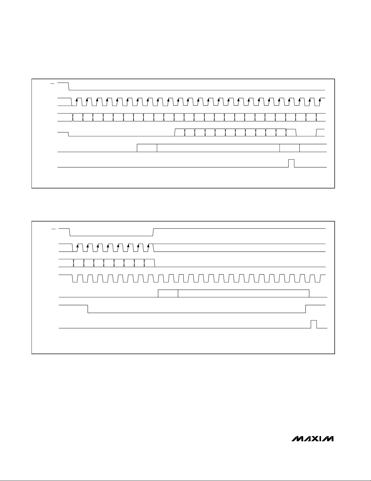
MAX1329/MAX1330
12-/16-Bit DASs with ADC, DACs, DPIOs, APIOs,
Reference, Voltage Monitors, and Temp Sensor
36 ______________________________________________________________________________________
Figure 18. Write Command to Start ADC Burst Conversions Clocked by SCLK with Real-Time Data Read (ACQCK<1:0> = 00,
GAIN<1:0> = 00)
Figure 19. Write Command to Start ADC Normal or Fast Power-Down, with Autoconvert Disabled (AUTO<2:0> = 000) and
Conversions Clocked by CLKIO (OSCE = 0, ADDIV<1:0> = 00, CLKIO<1:0> = 11)
CS
SCLK
DIN
DOUT
ADC MODE
ADCDONE*
*ADCDONE IS AN INTERNAL SIGNAL. RISING EDGE OF ADCDONE SETS THE ADD BIT IN THE STATUS REGISTER.
X = DON'T CARE.
123
1M3M2M1
X
45
M0
6 7 8 9 10 11 12 13 14 15 16 17 18
G1 G0 BIP
X
TRACK CONVERT TRACK CONVERT
XXXXXXXX
X X
D
D
D
11
10
9D8D7D6D5D4D3D2D1
19 20
XX
21
X
22
X
D
0
CS
SCLK
DIN
123 6 7845
1 M3M2M1M0G1 G0 BIP
X
24
23
X
25
X
D
11
CLKIO
ADC MODE
PD*
ADCDONE**
*PD IS AN INTERNAL SIGNAL. WHEN PD IS HIGH, THE ADC IS POWERED-DOWN.
**ADCDONE IS AN INTERNAL SIGNAL. RISING EDGE ADCDONE SETS THE ADD BIT IN THE STATUS REGISTER.
X = DON'T CARE.
12 3 6 78 9101112131415161745
TRACK CONVERT
Page 37

MAX1329/MAX1330
12-/16-Bit DASs with ADC, DACs, DPIOs, APIOs,
Reference, Voltage Monitors, and Temp Sensor
______________________________________________________________________________________ 37
Once configured, autoconvert mode initiates with one
ADC Convert command. Conversions continue at the
rate selected by the ADC Autoconvert bits (see Table 4)
until disabled by writing to the ADC Control register. The
Autoconvert mode can run only in the normal or fast
power-down modes. The autoconvert function must be
disabled to use burst mode or DPIO CONVST mode.
When writing to the ADC Control register in fast powerdown mode with autoconvert disabled, acquisition
begins on the 1st rising ADC clock edge after CS tran-
sitions high, and ends after the programmed number of
clock cycles. The conversion completes a minimum 14
clock cycles after acquisition ends. When autoconvert
is enabled, an additional three ADC clock cycles are
added prior to acquisition to allow the ADC to wake up.
See Figures 19 and 20 for timing diagrams.
Figure 20. Write Command to Start ADC Normal or Fast Power-Down, with Autoconvert Enabled and Conversions Clocked by CLKIO
(OSCE = 0, ADDIV<1:0> = 00, CLKIO<1:0> = 11)
Figure 21. DPIO-Controlled ADC Conversion Start
CS
SCLK
DIN
CLKIO
ADC MODE
PD*
ADCDONE**
*PD IS AN INTERNAL SIGNAL. WHEN PD IS HIGH, THE ADC IS POWERED DOWN.
**ADCDONE IS AN INTERNAL SIGNAL. RISING EDGE ADCDONE SETS THE ADD BIT IN THE STATUS REGISTER.
X = DON'T CARE.
123 67845
1M3M2M1
X
M0
G1 G0 BIP
123 678910111213181945
TRACK
CONVERT
CLKIO
ADC MODE
DPIO (CONVST)
PD*
ADCDONE**
*PD IS AN INTERNAL SIGNAL. WHEN PD IS HIGH, THE ADC IS POWERED DOWN.
**ADCDONE IS AN INTERNAL SIGNAL. RISING EDGE ADCDONE SETS THE ADD BIT IN THE STATUS REGISTER.
ADDIV = 00.
1 2 3 4 5 6 7 8 9 10111213141516 17181920 212223
CONVERT
EDGE TRIGGERED
TRACKTRACK
CONVERT
Page 38

MAX1329/MAX1330
12-/16-Bit DASs with ADC, DACs, DPIOs, APIOs,
Reference, Voltage Monitors, and Temp Sensor
38 ______________________________________________________________________________________
See Figure 21 for performing an ADC conversion using
a DPIO input programmed as CONVST. Allow at least
600ns for acquisition while the DPIO input is low and
the acquisition ends on the rising edge of the DPIO.
The conversion requires an additional 14 ADC clock
cycles. If the PGA gain is set to 4 or 8, the minimum
acquisition time is 1.2µs due to the increase of the input
sampling capacitor.
Temperature Measurement
The MAX1329/MAX1330 perform temperature measurement by measuring the voltage across a diode-connected transistor at two different current levels. The
following equation illustrates the algorithm used for temperature calculations:
where:
V
HIGH
= sensor-diode voltage with high current flowing
(I
HIGH
)
V
LOW
= sensor-diode voltage with low current flowing
(I
LOW
)
q = charge of electron = 1.602
✕ 10
-19
coulombs
k = Boltzman constant = 1.38 ✕ 10
-23
J/K
n = ideality factor (slightly greater than 1)
The temperature measurement process is fully automated in the MAX1329/MAX1330. All steps are sequenced
and executed by the MAX1329/MAX1330 each time an
input channel (or an input channel pair) configured for
temperature measurement is scanned.
The resulting 12-bit, two’s complement number represents the sensor temperature in degrees Celsius, with
1 LSB = +0.125°C. Figure 22 shows the timing for a
temperature measurement.
An external 2.500V reference can be applied to
REFADJ, provided the internal reference is disabled
first. Use the temperature correction equation to obtain
the correct temperature:
T
ACT
= 0.997 x T
MEAS
- 0.91°C
Use the following equation when using the internal reference:
Figure 22. Temperature-Conversion Timing
CS
TEMP CONVERT COMMAND
(SCLK, DIN, DOUT NOT SHOWN)
ADC MODE TRACK
START
THERE ARE TWO ADC CONVERSIONS PER TEMPERATURE CONVERSION.
WAIT PERIOD
93.5 CLOCKS
1 CLOCK = 1/(ADC MASTER CLOCK FREQUENCY)
temperature V V x
()-
=
HIGH LOW
nxln
q
k
⎡
⎢
⎣
I
High
I
LOW
1ST AQUISITION
90 CLOCKS
1ST CONVERSION
19 CLOCKS
CONVERT
2ND AQUISITION
87 CLOCKS
TRACK
2ND CONVERSION
17.5 CLOCKS
CONVERT
STOP
⎤
⎥
⎦
TT T
=+ + ×−(.)(
ACT MEAS MEAS
270 63 1
.
2 500
V
RREFADJ
V
C)°
Page 39

MAX1329/MAX1330
12-/16-Bit DASs with ADC, DACs, DPIOs, APIOs,
Reference, Voltage Monitors, and Temp Sensor
______________________________________________________________________________________ 39
Table 3. Register Summary
Note: R/W = 0 for write, R/W = 1 for read, X = don’t care.
*
Data length can vary from 1 to 16 words, where a word is 16 bits (12 data bits plus 4 address bits).
Register Definitions
REGISTER
NAME
ADC Control 0 0 R/W 0 0 0 0 0 AUTO<2:0> APD<1:0> AREF<1:0> REFE
ADC Setup 0 0 R/W 0 0 0 0 1 MSEL MUX<3:0> GAIN<1:0> BIP
ADC Data 0 0 1 0 0 0 1 0 ADCDATA<11:0> XXXX
ADC FIFO 0 0
ADC Accumulator 0 0
ADC GT Alarm 0 0 R/W 0 0 1 0 1 GTAM GTAC<2:0> GTAT<11:0>
ADC LT Alarm 0 0 R/W 0 0 1 1 0 LTAM LTAC<2:0> LTAT<11:0>
DAC Control 0 0 R/W 0 0 1 1 1 DAPD1
FIFOA Control 0 0 R/W 0 1 0 0 0 FFAE BIPA SYMA CONA DPTA<3:0>
Reserved 0 0 X 0 1 0 0 1
FIFOA Data 0 0 R/W 0 1 0 1 0 FFADATA<11:0> XXXX
Reserved 0 0 X 0 1 0 1 1 RESERVED, DO NOT USE
FIFO Sequence 0 0 W 01100XXXXXXXX
Clock Control 0 0 R/W 0 1 1 0 1 ODLY OSCE CLKIO<1:0> ADDIV<1:0> ACQCK<1:0>
CP/VM Control 0 0 R/W 0 1 1 1 0 INTP VM1<1:0> VM2CP<2:0> CPDIV<1:0>
Switch Control 0 0 R/W 01111
APIO Control 0 0 R/W 1 0 0 0 0 AP4MD<1:0> AP3MD<1:0> AP2MD<1:0> AP1MD<1:0>
APIO Setup 0 0 R/W 1 0 0 0 1 AP4PU AP3PU AP2PU AP1PU AP4LL AP3LL AP2LL AP1LL
DPIO Control 0 0 R/W 10010
DPIO Setup 0 0 R/W 1 0 0 1 1 DP4PU DP3PU DP2PU DP1PU DP4LL DP3LL DP2LL DP1LL
Status 0 0 R 1 0 1 0 0
Reserved 0 0 X 1 0 1 1 0 RESERVED, DO NOT USE
Reserved 0 0 X 1 0 1 1 1 RESERVED, DO NOT USE
Reserved 0 0 X 1 1 0 0 0 RESERVED, DO NOT USE
START
READ/
WRITE
(R/W)
0 AFFD<3:0> AFFI<3:0>
1
0 DITH ACCC<2:0> XXXX
1
ADDRESS
(ADR<4:0>)
00011
00100
DATA
(D<255:0>, D<23:0>, D<15:0>, OR D<7:0>)
AFFDATA<11:0>* AFFA<3:0>*
DITH ACCC<2:0> ACCDATA<19:0>
DAPD0/
OA3E
DSWA/
OSW3
VM1A VM1B VM2 ADD AFF ACF GTA LTA
MV1A MV1B MV2 MADD MAFF MACF MGTA MLTA
DSWB OSW1 OSW2 SPDT1<1:0> SPDT2<1:0>
DP4MD<3:0> DP3MD<3:0>
DP2MD<3:0> DP1MD<3:0>
DBPD1
APR<4:1> APF<4:1>
DPR<4:1> DPF<4:1>
MAPR<4:1> MAPF<4:1>Interrupt Mask 0 0 R/W 10101
MDPR<4:1> MDPF<4:1>
DBPD0/
OA2E
RESERVED, DO NOT USE
OA1E DREF<1:0> REFE
Page 40

MAX1329/MAX1330
12-/16-Bit DASs with ADC, DACs, DPIOs, APIOs,
Reference, Voltage Monitors, and Temp Sensor
40 ______________________________________________________________________________________
Table 3. Register Summary (continued)
Note: R/W = 0 for write, R/W = 1 for read, X = don’t care.
*
Data length can vary from 1 to 16 words, where a word is 16 bits (12 data bits plus 4 address bits).
Register Bit Descriptions
ADC Control Register
The ADC Control register configures the autoconvert
mode, the ADC power-down modes, the ADC reference
buffer, and the internal reference voltage. Changes
made to the ADC Control register settings are applied
immediately. If changes are made during a conversion
in progress, discard the results of that conversion to
ensure a valid conversion result.
AUTO<2:0>: ADC Autoconvert bits (default = 000). The
AUTO<2:0> bits configure the ADC to continuously convert at the selected interval (see Table 4). Calculate the
conversion rate by dividing the ADC master clock frequency by the selected number of clock cycles. For
example, if the ADC master clock frequency is
3.6864MHz and the selected value is 256, the conversion
rate is 3.6864MHz/256 or 14.4ksps. The conversion can
be started with the ADC Direct Write command and runs
continuously using the ADC master clock. Write 000 to
the AUTO<2:0> bits to disable autoconvert mode. When
the autoconvert ADC master clock cycle rate is set to 32
and the acquisition time is set to 32 (AUTO<2:0> = 001,
ACQCK<1:0> = 11, and GAIN<1:0> = 1X), the acquisition time is automatically reduced to 16 clocks so that the
ADC throughput is less than the autoconversion interval.
The automode operation is unavailable in burst mode.
APD<1:0>: ADC Power-Down bits (default = 00). The
APD<1:0> bits control the power-down states of the
ADC and PGA (see Table 5). When a direct-mode ADC
conversion command is received, the ADC and PGA
power up except when APD<1:0> = 00.
The burst mode outputs data to DOUT directly in real
time as the bit decision is made on the falling edge of
SCLK and the latest conversion result is also stored in
the ADC Data register. For this mode, the conversion
rate is controlled by the SCLK frequency, which is limited
to 5MHz. If the charge pump is enabled, synchronize
SCLK with the CLKIO clock to prevent charge-pump
noise from corrupting the ADC result. Initiate the conversion by writing to the ADC Control register. SCLK is
required to run continuously during the conversion period. For ADC gains of 1 or 2, a total of 14 to 28 clocks
(two to 16 for acquisition and 12 for conversion) are
required to complete the conversion. For ADC gains of 4
or 8, a total of 16 to 44 clocks (four to 32 for acquisition,
and 12 for conversion) are required to complete the conversion. Bringing CS high aborts burst mode.
AREF<1:0>: ADC Reference Buffer bits (default = 00).
The AREF<1:0> bits set the ADC reference buffer gain
when REFE = 0 and the REFADC output voltage when
REFE = 1 (see Table 6). Set AREF<1:0> to 00 to disable the ADC reference buffer and drive REFADC
directly with an external reference.
REFE: Internal Reference Enable bit (default = 0). REFE
= 1 enables the internal reference and sets REFADJ to
2.5V. REFE = 0 disables the internal reference, allowing
an external reference to be applied at REFADJ, which
drives the inputs to the ADC and DAC reference
buffers. The voltage at REFADJ is also used for temperature measurement and must be 2.5V for accurate
results. See the
Temperature Sensor
section. This bit is
mirrored in the DAC Control register so that writing
either location updates both bits.
REGISTER
NAME
Reserved 0 0 X 1 1 0 0 1 RESERVED, DO NOT USE
Reserved 0 0 X 1 1 0 1 0 RESERVED, DO NOT USE
Reserved 0 0 X 1 1 0 1 1 RESERVED, DO NOT USE
Reserved 0 0 X 1 1 1 0 0 RESERVED, DO NOT USE
Reserved 0 0 X 1 1 1 0 1 RESERVED, DO NOT USE
Reserved 0 0 X 1 1 1 1 0 RESERVED, DO NOT USE
Reset 0 0 W 11111XXXXXXX X
START
NAME AUTO2 AUTO1 AUTO0 APD1 APD0 AREF1 AREF0 REFE
DEFAULT 00000000
MSB LSB
READ/
WRITE
(R/W)
ADDRESS
(ADR<4:0>)
DATA
(D<255:0>, D<23:0>, D<15:0>, OR D<7:0>)
Page 41

MAX1329/MAX1330
12-/16-Bit DASs with ADC, DACs, DPIOs, APIOs,
Reference, Voltage Monitors, and Temp Sensor
______________________________________________________________________________________ 41
Table 5. ADC Power-Down Bit Configuration
Table 6. ADC Reference-Buffer Bit Configuration
Table 4. ADC Autoconvert Bit
Configuration (AUTO<2:0>)
AUT02 AUTO1 AUTO0
0 0 0 Autoconvert disabled
00 1 32
01 0 64
0 1 1 128
1 0 0 256
1 0 1 512
1 1 0 1024
1 1 1 2048
APD1 APD0 ADC MODE COMMENTS
0 0 Power-down ADC/PGA off
0 1 Fast power-down ADC/PGA off between conversions
1 0 Normal ADC/PGA on
1 1 Burst
ADC MASTER CLOCK
CYCLES
ADC/PGA on, SCLK clocks conversion, data clocked out on DOUT in real time on
the falling edge of SCLK
AREF1 AREF0
0 0 Buffer off High-impedance
0 1 0.5 1.25
1 0 0.8192 2.048
1 1 1 2.5
ADC REFERENCE-BUFFER GAIN (V/V)
(REFE = 0)
REFADC VOLTAGE (V)
(REFE = 1)
Page 42

MAX1329/MAX1330
12-/16-Bit DASs with ADC, DACs, DPIOs, APIOs,
Reference, Voltage Monitors, and Temp Sensor
42 ______________________________________________________________________________________
ADC Setup Register
The ADC Setup register configures the input multiplexer,
ADC gain, and unipolar/bipolar modes to perform a data
conversion. Changes made to the ADC Setup register
settings are applied immediately. If changes are made
during a conversion in progress, discard the results of
that conversion to ensure a valid conversion result.
MSEL: Multiplexer Select bit (default = 0). The MSEL bit
selects the upper or lower multiplexer. MSEL = 0 selects
the upper mux and MSEL = 1 selects the lower mux.
MUX<3:0>: Multiplexer Input Select bits (default =
0000). The MUX<3:0> bits plus the MSEL bit select the
inputs to the ADC (see Tables 7 and 8).
GAIN<1:0>: ADC Gain bits (default = 00). The
GAIN<1:0> bits select the gain of the ADC (see Table 9).
BIP: Unipolar-/Bipolar-Mode Selection bit (default = 0).
For unipolar mode, set BIP = 0. For bipolar mode, set
BIP = 1. For temperature-sensor conversions, use the
default GAIN = 00 and BIP = 0.
Table 7. Upper Multiplexer Bit Configuration (MSEL = 0)
MSB LSB
NAME MSEL MUX3 MUX2 MUX1 MUX0 GAIN1 GAIN0 BIP
DEFAULT 00000000
MUX3 MUX2 MUX1 MUX0
0 0 0 0 AIN1 AGND
0 0 0 1 AIN2 AGND
0 0 1 0 OUTA AGND
0 0 1 1 FBA AGND
0 1 0 0 OUT1 AGND
0 1 0 1 IN1- AGND
0 1 1 0 OUTB OUT2 AGND
0 1 1 1 FBB IN2- AGND
1 0 0 0 AIN1 AIN2
1 0 0 1 AIN2 AIN1
1010 OUTA FBA
1 0 1 1 FBA OUTA
1 1 0 0 OUT1 IN1-
1 1 0 1 IN1- OUT1
1 1 1 0 OUTB OUT2 FBB IN2-
1 1 1 1 FBB IN2- OUTB OUT2
MAX1329 MAX1330 MAX1329 MAX1330
POSITIVE INPUT NEGATIVE INPUT
Page 43

MAX1329/MAX1330
12-/16-Bit DASs with ADC, DACs, DPIOs, APIOs,
Reference, Voltage Monitors, and Temp Sensor
______________________________________________________________________________________ 43
Table 8. Lower Multiplexer Bit Configuration (MSEL = 1)
Table 9. ADC Gain Bit Configuration
MUX3 MUX2 MUX1 MUX0
0 0 0 0 AIN1 REFADC
0 0 0 1 OUTA REFADC
0 0 1 0 OUT1 REFADC
0 0 1 1 OUTB OUT2 REFADC
0 1 0 0 AIN1 REFDAC
0 1 0 1 OUTA REFDAC
0 1 1 0 OUT1 REFDAC
0 1 1 1 OUTB OUT2 REFDAC
1000
1001
1010
1011
1100 DV
1101 AV
1 1 1 0 REFADC AGND
1 1 1 1 REFDAC AGND
POSITIVE INPUT NEGATIVE INPUT
MAX1329 MAX1330 MAX1329 MAX1330
TEMP1+
(Internal diode anode)
TEMP2+
(External diode anode at AIN1)
TEMP3+
(External diode anode at AIN1)
TEMP4+
(External diode anode at AIN2)
/4 AGND
DD
/4 AGND
DD
(Internal diode cathode)
(External diode cathode at AIN2)
TEMP1-
TEMP2-
AGND
AGND
GAIN1 GAIN0 ADC GAIN SETTING (V/V)
00 1
01 2
10 4
11 8
Page 44

MAX1329/MAX1330
12-/16-Bit DASs with ADC, DACs, DPIOs, APIOs,
Reference, Voltage Monitors, and Temp Sensor
44 ______________________________________________________________________________________
ADC Data Register
The ADC Data register contains the result from the most
recently completed analog-to-digital conversion. The
12-bit result is stored in the ADCDATA<11:0> bits. The
data format is binary for unipolar mode and two’s complement for bipolar mode. The ADC Data register contents are the same as the ADC FIFO contents at the last
written address, unless writes to the ADC FIFO have
been inhibited.
ADC FIFO Register
The ADC FIFO register contents are different for write
and read modes. In write mode, the ADC FIFO register
sets the working depth of the FIFO and the address that
generates an interrupt. In read mode, the ADC FIFO
register holds the ADC FIFO data and FIFO address.
Write Format
A serial interface write to the ADC FIFO register moves
the FIFO write and read pointers to address 0.
AFFD<3:0>: ADC FIFO Depth bits (default = 0000).
AFFD<3:0> sets the working depth of the FIFO (see
Table 10). If set to a depth of zero, the ADC FIFO is disabled and writes to the AFF (ADC FIFO Full) bit in the
Status register are also disabled. AFFD<3:0> are writeonly bits.
AFFI<3:0>: ADC FIFO Interrupt Address bits (default =
0000). AFFI<3:0> sets the FIFO address. After each
successful ADC conversion, the conversion results are
transferred from the ADC Data register to the FIFO
location indicated by the FIFO write pointer, and the
FIFO write pointer is incremented. When the FIFO write
pointer exceeds the value in AFFI<3:0>, the AFF bit in
the Status register (Table 11) is asserted. Set the
AFFI<3:0> value equal to or less than the AFFD<3:0>
value. If set to a value greater than AFFD<3:0>,
AFFI<3:0> is forced to the AFFD<3:0> value. If
AFFD<3:0> is set to 0000 (depth of zero), the ADC
FIFO is disabled and writes to the AFF bit are also disabled. AFFI<3:0> are write-only bits.
X = Don’t care.
NAME ADCDATA11 ADCDATA10 ADCDATA9 ADCDATA8 ADCDATA7 ADCDATA6 ADCDATA5 ADCDATA4
DEFAULT 00000000
NAME ADCDATA3 ADCDATA2 ADCDATA1 ADCDATA0 X X X X
DEFAULT 0000XXXX
NAME AFFD3 AFFD2 AFFD1 AFFD0 AFFI3 AFFI2 AFFI1 AFFI0
DEFAULT 00000000
MSB
LSB
MSB LSB
Page 45

MAX1329/MAX1330
12-/16-Bit DASs with ADC, DACs, DPIOs, APIOs,
Reference, Voltage Monitors, and Temp Sensor
______________________________________________________________________________________ 45
Table 10. ADC FIFO Depth Bit
Configuration
Table 11. ADC FIFO Interrupt-Address Bit
Configuration
Note: Data length can vary from 1 to 16 words, where a word is 16 bits (12 data bits plus 4 address bits).
Read Format
A single read from the ADC FIFO register returns the
ADC FIFO data and the 4-bit FIFO address (AFFA<3:0>)
corresponding to the location read.
After clocking out the 16-bit word, the read pointer
increments and continual clock shifts out the 16-bit
word at the location pointed to by the ADC FIFO read
pointer. If trying to read from the ADC FIFO at a location
pointed to by the ADC FIFO write pointer, the FIFO
repeats the last ADC conversion result and corresponding ADC FIFO address equivalent to the ADC FIFO
write pointer. To stop reading, bring CS high after
clocking out the 16th bit of a complete word. The read
pointer increments after each complete 16-bit word
read. It does not increment if the read is aborted by
bringing CS high before clocking out all 16 bits. Any
read operation on the ADC FIFO register resets the
interrupt flag (AFF).
AFFDATA<11:0>: ADC FIFO Read Data bits (default =
0000 0000 0000). AFFDATA<11:0> returns the data
written by the ADC at the current read pointer location.
AFFA<3:0>: ADC FIFO Read Address bits (default =
0000). AFFA<3:0> returns the address of the current
read pointer location. AFFA<3:0> is never greater than
the AFFD<3:0> programmed value.
MSB
NAME AFFDATA11 AFFDATA10 AFFDATA9 AFFDATA8 AFFDATA7 AFFDATA6 AFFDATA5 AFFDATA4
DEFAULT 00000000
LSB
NAME AFFDATA3 AFFDATA2 AFFDATA1 AFFDATA0 AFFA3 AFFA2 AFFA1 AFFA0
DEFAULT 00000000
AFFD3 AFFD2 AFFD1 AFFD0
0 0 0 0 FIFO disabled
0 0 0 1 2 0-1
0 0 1 0 3 0-2
0 0 1 1 4 0-3
0 1 0 0 5 0-4
0 1 0 1 6 0-5
0 1 1 0 7 0-6
0 1 1 1 8 0-7
1 0 0 0 9 0-8
1 0 0 1 10 0-9
1 0 1 0 11 0-10
1 0 1 1 12 0-11
1 1 0 0 13 0-12
1 1 0 1 14 0-13
1 1 1 0 15 0-14
1 1 1 1 16 0-15
ADC FIFO
WORD
DEPTH
WRITE
POINTER
RANGE
AFFI3 AFFI2 AFFI1 AFFI0
0000 0
0001 1
0010 2
0011 3
0100 4
0101 5
0110 6
0111 7
1000 8
1001 9
1010 10
1011 11
1100 12
1101 13
1110 14
1111 15
ADC FIFO
INTERRUPT
ADDRESS
Page 46

MAX1329/MAX1330
12-/16-Bit DASs with ADC, DACs, DPIOs, APIOs,
Reference, Voltage Monitors, and Temp Sensor
46 ______________________________________________________________________________________
Read Format
ADC Accumulator Register
The ADC Accumulator register contains the bits to
enable dither, set the accumulator count, and set the
20-bit accumulator data. The dither and accumulator
count bits are read/write and the accumulator data is
read only. A write to the register resets the accumulator
data (ACCDATA<19:0>) to 0x00000 and starts new
accumulation. The ACCDATA<19:0> bits remain
unchanged until the programmed count of conversions is completed. The accumulator is functional for
the normal, fast power-down, and burst modes.
DITH: Dither bit (default = 0). When DITH = 0, the dither
generator is disabled and the accumulator can be used
for oversampling and providing digital filtering (see the
Applying a Digital Filter to ADC Data Using the 20-Bit
Accumulator
section). When DITH = 1, the dithering for
the ADC is enabled. Use dithering with the accumulator
to oversample data and decimate the result to extend the
effective resolution to a maximum of 16 bits and provide
digital filtering.
ACCC<2:0> ADC Accumulator Count bits (default =
000). The ACCC<2:0> bits set the number of ADC data
conversion results to be accumulated and then written to
the ACCDATA register before the ACF Status bit is set
(see Table 12). The ACF status bit is set in the Status
register when the data is written to the ACCDATA register. If the accumulator count is set to 1, the accumulator
does not accumulate and the ACCDATA<11:0> is the
same as ADCDATA<11:0> in the ADC Data register.
ACCDATA<19:0>: ADC Accumulator Data bits (default =
0x00000). The ACCDATA<19:0> bits are the summation
of up to 256 ADC conversion results. When the count set
by ACCC<2:0> has been reached, the ACF status bit is
set and the accumulated data is written to this register.
The data is written to the register at a rate of the ADC
conversion rate divided by the accumulator count. The
accumulator does not exceed 0xFFFFF.
X = Don’t care.
Write Format
Table 12. ADC Accumulator-Count Bit
Configuration
NAME DITH ACCC2 ACCC1 ACCC0 XXXX
DEFAULT 0000XXXX
NAME DITH ACCC2 ACCC1 ACCC0 ACCDATA19 ACCDATA18 ACCDATA17 ACCDATA16
DEFAULT 00000000
MSB LSB
MSB
NAME ACCDATA15 ACCDATA14 ACCDATA13 ACCDATA12 ACCDATA11 ACCDATA10 ACCDATA9 ACCDATA8
DEFAULT 00000000
LSB
NAME ACCDATA7 ACCDATA6 ACCDATA5 ACCDATA4 ACCDATA3 ACCDATA2 ACCDATA1 ACCDATA0
DEFAULT 00000000
ACCC2 ACCC1 ACCC0 ACCUMULATOR COUNT
000 1
001 4
010 8
011 16
100 32
101 64
110 128
111 256
Page 47

MAX1329/MAX1330
12-/16-Bit DASs with ADC, DACs, DPIOs, APIOs,
Reference, Voltage Monitors, and Temp Sensor
______________________________________________________________________________________ 47
ADC GT Alarm Register
The ADC GT Alarm register contains the greater-than
mode, trip count, and threshold settings. A write to this
register address resets the trip counters to zero. The
GT alarm is functional for the normal, fast power-down,
and burst modes.
GTAM: ADC Greater-Than Alarm Mode bit (default = 0).
GTAM = 0 means that the alarm trips do not need to be
consecutive before the GTA Status bit is set. When
GTAM = 1, the alarm trips must be consecutive to set
the GTA Status bit.
GTAC<2:0>: ADC Greater-Than Alarm Trip Count bits
(default = 000). GTAC<2:0> set the number of conversion
results needed to be greater than the alarm threshold
before the GTA Status bit is set (see Table 13).
GTAT<11:0>: ADC Greater-Than Alarm Threshold bits
(default = 0xFFF). When the required number of conversion results greater than the threshold set by the
GTAT<11:0> bits have been completed, the GTA Status
bit is set in the Status register. Clearing the GTA Status
bit by reading the Status register or writing to the ADC
GT Alarm register restarts the trip count. The
GTAT<11:0> bits are in binary format when the ADC is in
unipolar mode and two’s complement format when the
ADC is in bipolar mode. Disable the GT alarm by setting
GTAT<11:0> to 0xFFF when the ADC is in unipolar mode
and 0x7FF when the ADC is in bipolar mode.
Table 13a. ADC Greater-Than Alarm Trip
Count Bit Configuration
MSB
NAME GTAM GTAC2 GTAC1 GTAC0 GTAT11 GTAT10 GTAT9 GTAT8
DEFAULT 00001111
NAME GTAT7 GTAT6 GTAT5 GTAT4 GTAT3 GTAT2 GTAT1 GTAT0
DEFAULT 11111111
LSB
GTAC2 GTAC1 GTAC0 NUMBER OF TRIPS
000 1
001 2
010 3
011 4
100 5
101 6
110 7
111 8
Page 48

MAX1329/MAX1330
12-/16-Bit DASs with ADC, DACs, DPIOs, APIOs,
Reference, Voltage Monitors, and Temp Sensor
48 ______________________________________________________________________________________
ADC LT Alarm Register
The ADC LT Alarm register contains the less-than
mode, trip count, and threshold settings. Writing the
register address resets the trip counters to zero. The LT
alarm is functional for the normal, fast power-down, and
burst modes.
LTAM: ADC Less-Than Alarm Mode bit (default = 0).
LTAM = 0 means that the alarm trips need not be consecutive to cause the LTA Status bit to be set. LTAM = 1
means that the alarm trips must be consecutive before
the LTA Status bit is set.
LTAC<2:0>: ADC Less-Than Alarm Trip Count bits
(default = 000). LTAC<2:0> set the number of conversion results needed to be less than the alarm threshold
before the LTA Status bit is set.
LTAT<11:0>: ADC Less-Than Alarm Threshold bits
(default = 0x000). When the required number of ADC
conversions results less than the threshold set by the
LTAT<11:0> bits have been completed, the LTA Status
bit is set in the Status register. Clearing the LTA Status
bit by reading the Status register or writing to the ADC LT
Alarm register restarts the trip count. The LTAT<11:0>
bits are in binary format when the ADC is in unipolar
mode and two’s complement format when the ADC is in
bipolar mode. Disable the LT alarm by setting
LTAT<11:0> to 0x000 when the ADC is in unipolar mode
and 0x800 when the ADC is in bipolar mode.
Table 13b. ADC Less-Than Alarm Trip
Count Bit Configuration
MSB
NAME LTAM LTAC2 LTAC1 LTAC0 LTAT11 LTAT10 LTAT9 LTAT8
DEFAULT 00000000
NAME LTAT7 LTAT6 LTAT5 LTAT4 LTAT3 LTAT2 LTAT1 LTAT0
DEFAULT 00000000
LSB
LTAC2 LTAC1 LTAC0 NUMBER OF TRIPS
000 1
001 2
010 3
011 4
100 5
101 6
110 7
111 8
Page 49

MAX1329/MAX1330
12-/16-Bit DASs with ADC, DACs, DPIOs, APIOs,
Reference, Voltage Monitors, and Temp Sensor
______________________________________________________________________________________ 49
DAC Control Register
The DAC Control register configures the power states for
DACA, DACB, the op amps, DAC reference buffer, and
the internal reference. The DAC Control register also
controls the DACA and DACB input and output register
write modes. At power-up, all DACs and op amps are
powered down. When powered down, the outputs of the
DAC buffers and op amps are high impedance.
DAPD<1:0>: DACA Power-Down bits (default = 00).
DAPD<1:0> control the power-down states and write
modes for DACA (see Table 14).
DBPD<1:0>: (MAX1329 only) DACB Power-Down bits
(default = 00). DBPD<1:0> control the power-down states
and write modes for a DACB write as shown in Table 15.
OA1E: Op Amp 1 Enable bit (default = 0). Set OA1E = 1
to power up op amp 1.
OA2E (MAX1330 only): Op Amp 2 Enable bit (default =
0). Set OA2E = 1 to power up op amp 2.
DREF<1:0>: DAC Reference Buffer bits (default = 00).
DREF<1:0> sets the DAC reference buffer gain when
REFE = 0 (see Table 16). DREF<1:0> sets the REFDAC
voltage when the REFE = 1.
REFE: Internal Reference Enable bit (default = 0). REFE
= 1 enables the internal reference and sets REFADJ to
2.5V. REFE = 0 disables the internal reference so an
external reference can be applied at REFADJ, which
drives the inputs to the ADC and DAC reference
buffers. This bit is mirrored in the ADC Control register
so that writing either location updates both bits.
Table 14. DACA Power-Down Bit
Configuration
Table 15. DACB Power-Down Bit
Configuration (MAX1329 Only)
MAX1329
MSB LSB
NAME DAPD1 DAPD0 DBPD1 DBPD0 OA1E DREF1 DREF0 REFE
DEFAULT 0 0000000
MAX1330
MSB LSB
NAME DAPD1 DAPD0 X OA2E OA1E DREF1 DREF0 REFE
DEFAULT 0 0X00000
DAPD1 DAPD0
0 0 Powered down
0 1 Powered up
1 0 Powered up Write input register
1 1 Powered up
DACA POWER
MODE
DACA WRITE MODE
Write input and output
register
Write input and output
register
Shift input to output
register
DBPD1 DBPD0
0 0 Powered down
0 1 Powered up
1 0 Powered up Write input register
1 1 Powered up
DACB POWER
MODE
DACB WRITE
MODE
Write input and
output register
Write input and
output register
Shift input to output
register
Page 50

MAX1329/MAX1330
12-/16-Bit DASs with ADC, DACs, DPIOs, APIOs,
Reference, Voltage Monitors, and Temp Sensor
50 ______________________________________________________________________________________
FIFOA Control Register
The FIFOA Control register enables the DACA FIFO,
configures the bipolar, symmetry, and continuous
modes, and sets the depth of the FIFO. Any change to
the contents of this register resets the FIFOA sequence
to the starting location. If the FIFO operation is enabled
(FFAE = 1), the next sequence command transfers the
DACA input register data to the output register. The
DACA input or output register can be written to when
the FIFO is enabled without affecting the FIFOA
sequence, but the DACA output and/or input register
data is changed.
FFAE: DACA FIFO Enable bit (default = 0). Set FFAE = 1
to enable the sequencing function. FFAE must be set to
0 to write to the FIFO. Writes to the FIFO when FFAE = 1
are ignored.
BIPA: DACA FIFO Bipolar bit (default = 0). Set BIPA = 0
to generate a unipolar waveform or set BIPA = 1 to generate a bipolar waveform. For a unipolar waveform, the
FIFOA data is added to the DACA input register data
during phases 1 and 2 (see Figures 8 and 9).
For a bipolar waveform, the FIFOA data is added to the
DACA input register data (during phases 1 and 2) and
subtracted from the DACA input register data (during
phases 3 and 4).
SYMA: DACA FIFO Symmetry bit (default = 0). Set
SYMA = 0 to generate an asymmetrical waveform, consisting of phase 1 (BIPA = 0) or phases 1 and 4 (BIPA
= 1). Set SYMA = 1 to generate symmetry phases 1
and 2 (BIPA = 0) or phases 1–4 (BIPA = 1).
CONA: DACA FIFO Continuous bit (default = 0). Set
CONA = 0 to generate a single waveform or set CONA
= 1 to generate a periodic or continuous waveform.
DPTA<3:0>: DACA FIFO Depth bits (default = 0000).
The DPTA<3:0> bits set the depth of the FIFOA data
register to be used for waveform generation (see Table
17). The entire FIFOA data register can be filled with 16
words but only the number programmed by
DPTA<3:0> are used. During waveform generation, the
FIFOA words are added to the DACA input register
value before being sent to the DACA output register.
The first output is the DACA input register value. The
following value is the DACA input register value
summed with the FIFOA location 1 value. The FIFOA
locations are incremented until the FIFO depth specified by the DPTA<3:0> bits has been reached.
Table 16. DAC Reference Buffer Bit
Configuration
MSB LSB
NAME FFAE BIPA SYMA CONA DPTA3 DPTA2 DPTA1 DPTA0
DEFAULT 00000000
DREF1 DREF0
0 0 N/A Buffer disabled
0 1 0.5 1.25
1 0 0.8192 2.048
1 1 1.0 2.5
DAC REFERENCE
BUFFER GAIN (V/V)
(REFE = 0)
REFDAC
VOLTAGE (V)
(REFE = 1)
Page 51

MAX1329/MAX1330
12-/16-Bit DASs with ADC, DACs, DPIOs, APIOs,
Reference, Voltage Monitors, and Temp Sensor
______________________________________________________________________________________ 51
FIFOA Data Register
The FIFOA Data register stores up to 16 12-bit words that
can be used by DACA to generate a waveform.
FFADATA<11:0>: FIFOA Data bits (default = 0xXXX).
FFADATA<11:0> represents a 12-bit word that is left
justified with 4 don’t-care LSBs. A write or read operation always starts at location 1 and ends at the full FIFO
depth. Any attempt to write past the full FIFO depth
does not overwrite the data just written. Any attempt to
read past the full FIFO depth returns zeroes on DOUT.
A write to the FIFOA Data register is possible only when
the FFAE bit in the FIFOA Control register is 0. If FFAE
= 1, any write to the FIFOA Data register is ignored. A
read command is possible at any time. If BIPA = 0, the
data is interpreted as binary (0 to 4095). If BIPA = 1,
the data is interpreted as sign magnitude (-2047 to
+2047). In sign magnitude, the MSB represents the
sign bit, where 0 indicates a positive number and 1
indicates a negative number. The 11 LSBs provide the
magnitude in sign magnitude.
Table 17. DACA FIFO Depth Bit
Configuration
X = Don’t care.
MSB
NAME FFADATA11 FFADATA10 FFADATA9 FFADATA8 FFADATA7 FFADATA6 FFADATA5 FFADATA4
DEFAULT 00000000
NAME FFADATA3 FFADATA2 FFADATA1 FFADATA0 XXXX
DEFAULT 0000XXXX
LSB
DPTA3 DPTA2 DPTA1 DPTA0 FIFOA DEPTH
0000 1
0001 2
0010 3
0011 4
0100 5
0101 6
0110 7
0111 8
1000 9
1001 10
1010 11
1011 12
1100 13
1101 14
1110 15
1111 16
Page 52

MAX1329/MAX1330
12-/16-Bit DASs with ADC, DACs, DPIOs, APIOs,
Reference, Voltage Monitors, and Temp Sensor
52 ______________________________________________________________________________________
FIFO Sequence Register
A write to the FIFO Sequence register steps DACA to the
next FIFOA word. A valid write consists of the 8-bit
address and 8 bits of data, where the data bits are don’tcare bits. The FIFO location increments on the 16th rising
edge of SCLK. Successive writes sequence the entire
contents of the FIFOA Data register to the DACA output
register. The FIFO can also be sequenced with the
DPIOs configured as DLDA or DLAB. The FIFO
Sequence register is a write-only register.
Clock Control Register
The Clock Control register enables the internal oscillator and the CLKIO output, sets the ADC acquisition
time, and controls the CLKIO, ADC, and charge-pump
programmable dividers.
ODLY: Oscillator Turn-Off Delay bit (default = 0). Set
ODLY = 0 to allow the oscillator to turn off immediately
when powered down by the OSCE bit. If ODLY = 1, the
oscillator turns off 1024 CLKIO clock cycles after it is
powered down by the OSCE bit. ODLY also affects
DPIO sleep mode (SLPB). When ODLY = 1, OSCE = 1,
and CLKIO<1:0> does not equal 00b, SLPB is delayed
by 1024 CLKIO clocks.
OSCE: Internal Oscillator Enable bit (default = 1). Set
OSCE = 1 to enable the internal 3.6864MHz oscillator.
Set OSCE = 0 to disable the internal oscillator and
apply an external oscillator at CLKIO. When turning off,
CLKIO drives low before becoming an input. Do not
leave CLKIO unconnected when configured as an
input. The APIOs and DPIOs can be configured as a
wake-up to set the OSCE bit.
CLKIO<1:0>: CLKIO Configuration bits (default = 10).
CLKIO<1:0> control the CLKIO input and output divider
settings. See Table 18 for the CLKIO configurations.
Changes to the CLKIO<1:0> bits occur on the falling
edge of CLKIO. The ODLY bit is ignored and has no
effect when the CLKIO is disabled. When OSCE = 1,
changing the CLKIO output frequency does not change
the frequency of the clock to the ADC and chargepump clock dividers. When OSCE = 0, the output of the
CLKIO input dividers is applied to the ADC and chargepump clock dividers. The changes can take up to four
CLKIO clock cycles due to internal synchronization.
ADDIV<1:0>: ADC Clock Divider bits (default = 00).
ADDIV<1:0> configures the ADC clock divider (see
Table 19), and the output is the ADC master clock
(Figure 3). If OSCE = 1, the input to the ADC clock
divider is the output of the 3.6864MHz oscillator. If
OSCE = 0 and CLKIO<1:0> ≠ 00, the output of the
CLKIO input divider is applied to the input of the ADC
clock divider.
ACQCK<1:0> ADC Acquisition Clock bits (default =
01). ACQCK<1:0> set the number of ADC master
clocks used for the ADC acquisition (see Table 20). For
gains of 1 or 2 (GAIN<1:0> = 0X in the ADC Control
register), the number of acquisition clocks can be set
for 2, 4, 8, or 16. For gains of 4 or 8 (GAIN<1:0> = 1X),
the number of acquisition clocks can be programmed
to be 4, 8, 16, or 32.
Table 18. CLKIO Bit Configuration
Table 19. ADC Clock Divider Bit
Configuration
MSB LSB
NAME ODLY OSCE CLKIO1 CLKIO0 ADDIV1 ADDIV0 ACQCK1 ACQCK0
DEFAULT 01100001
CLKIO1 CLKIO0
0 0 Input
01 f
10 f
11 f
CLKIO INPUT
MODE
(OSCE = 0)
/4 1.2288
CLKIO
/2 2.4567
CLKIO
CLKIO
CLKIO OUTPUT
MODE (MHz)
(OSCE = 1)
Disabled
(output low)
4.9152
ADDIV1 ADDIV0 ADC CLOCK DIVIDER
0 0 Divide by 1
0 1 Divide by 2
1 0 Divide by 4
1 1 Divide by 8
Page 53
MAX1329/MAX1330
12-/16-Bit DASs with ADC, DACs, DPIOs, APIOs,
Reference, Voltage Monitors, and Temp Sensor
______________________________________________________________________________________ 53
CP/VM Control Register
The CP/VM (Charge Pump/Voltage Monitor) Control
register configures the interrupt polarity, charge-pump
output voltage settings and power-down, supply voltage bypass switch state, and the voltage monitor settings for DVDDand AVDD.
INTP: Interrupt Polarity bit (default = 0). INTP controls
the output polarity for RST1 and RST2 when configured
as interrupt outputs. INTP = 0 results in active-low operation and INTP = 1 selects active-high operation.
VM1<1:0>: Voltage Monitor 1 (VM1) Control bits
(default = 00). VM1 monitors the voltage on DVDD. The
VM1<1:0> bits control the threshold and output settings
of VM1 (see Table 21). RST1 and RST2 are open-drain
outputs when configured as voltage monitor outputs
and are push-pull when configured as interrupt outputs.
The VM1A status bit is set when DVDDdrops below the
1.8V threshold and the VM1B status bit is set when
DVDDdrops below the 2.7V threshold.
VM2CP<2:0>: Voltage Monitor 2 (VM2) and ChargePump Control bits (default = 000). VM2CP<2:0> control
the charge pump, the bypass switch, and the AV
DD
voltage monitor. The charge pump generates a regulated
AVDDsupply voltage from a DVDDinput. When activated
(VM2CP = 100), the bypass switch internally shorts
DVDDto AVDD. VM2 monitors the voltage on AVDDand
sets the VM2 Status bit when AVDDdrops below
the threshold.
CPDIV<1:0>: Charge-Pump Clock Divider bits (default =
00). The CPDIV<1:0> bits set the divider value for the
input clock to the charge pump (see Table 23). If OSCE
= 1, the input to the charge-pump clock divider is the
3.6864MHz oscillator output. If OSCE = 0 and
CLKIO<1:0> ≠ 00, the output of the CLKIO input divider
is applied to the input of the charge-pump clock divider.
The charge pump is optimized to operate with a clock
rate between 39kHz and 78kHz. Set the CPDIV<1:0>
and CLKIO<1:0> bits to provide the optimal clock
frequency for the charge pump.
Table 21. Voltage Monitor 1 Control Bit Configuration
Table 20. ADC Acquisition Clock Bit
Configuration
MSB LSB
NAME INTP VM11 VM10 VM2CP2 VM2CP1 VM2CP0 CPDIV1 CPDIV0
DEFAULT 00000000
ACQCK1 ACQCK0
00 2 4
01 4 8
10 8 16
1 1 16 32
VM11 VM10 RST1 OUTPUT RST2 OUTPUT
0 0 1.8V monitor 2.7V monitor On On
0 1 1.8V monitor Interrupt On Off
1 0 Interrupt 2.7V monitor Off On
1 1 Interrupt Interrupt Off Off
ADC ACQUISITION CLOCKS
GAIN = 1, 2 GAIN = 4, 8
VM1A STATE
(1.8V MONITOR)
VM1B STATE
(2.7V MONITOR)
Page 54

MAX1329/MAX1330
12-/16-Bit DASs with ADC, DACs, DPIOs, APIOs,
Reference, Voltage Monitors, and Temp Sensor
54 ______________________________________________________________________________________
Table 22. Voltage Monitor 2 and Charge-Pump Control Bit Configuration
Table 23. Charge-Pump Clock Divider Bit
Configuration
VM2CP2 VM2CP1 VM2CP0 CHARGE-PUMP STATE BYPASS SWITCH STATE
0 0 0 Off Open Off
0 0 1 On (3V) Open On (2.7V)
0 1 0 On (4V) Open On (3.8V)
0 1 1 On (5V) Open On (4.5V)
1 0 0 Off Closed Off
1 0 1 Off Open On (2.7V)
1 1 0 Off Open On (3.6V)
1 1 1 Off Open On (4.5V)
CPDIV1 CPDIV0 CHARGE-PUMP CLOCK DIVIDER
0 0 Divide by 32
0 1 Divide by 64
1 0 Divide by 128
1 1 Divide by 256
VM2 STATE
(THRESHOLD VOLTAGE)
Page 55

MAX1329/MAX1330
12-/16-Bit DASs with ADC, DACs, DPIOs, APIOs,
Reference, Voltage Monitors, and Temp Sensor
______________________________________________________________________________________ 55
X = Don’t care.
Switch Control Register
The Switch Control register controls the two SPDT
switches and the feedback switches for DACA, DACB,
op amp 1, and op amp 2. The switches are controlled
through the serial interface or by a configured DPIO.
DSWA: DACA Switch Control bit (default = 0). The
DSWA bit controls the state of the DACA switch. A
logic-high in DSWA or on any DPIO_ configured as a
DACA switch control input causes the DACA switch to
close. The switch remains open when DSWA = 0 and
all DPIO_ pins configured as DACA switch control
inputs are logic-low. DPIO_ pins not configured as
DACA switch control inputs are treated as logic zeros.
See Table 24.
DSWB (MAX1329 only): DACB Switch Control bit
(default = 0). A logic-high in DSWB or an any DPIO_
configured as a DACB switch control input causes the
DACB switch to close. The switch remains open when
DSWB = 0 and all DPIO_s configured as DACB switch
control inputs are logic-low. DPIO_s not configured as
DACB switch control inputs are treated as logic zeros.
See Table 25.
OSW1: Op Amp 1 Switch Control bit (default = 0). The
OSW1 bit and DPIO_ configured in OSW1 mode control
the state of the op amp 1 switch. If DPIO_ is not configured for OSW1 mode, it is set to 0 as shown in Table 26.
OSW2 (MAX1330 only): Op Amp 2 Switch Control bit
(default = 0). The OSW2 bit and DPIO_ configured in
OSW2 mode control the state of the op amp 2 switch. If
DPIO_ is not configured for OSW2 mode, it is set to 0
as shown in Table 27.
SPDT1<1:0>: Single-Pole, Double-Throw Switch 1
(SPDT1) Control bits (default = 00). The SPDT1<1:0>
bits and DPIO_ configured for SPDT1 mode control the
state of the switch. If DPIO_ is not configured for SPDT1
mode, it is set to 0 as shown in Table 28.
SPDT2<1:0>: Single-Pole, Double-Throw Switch 2
(SPDT2) Control bits (default = 00). The SPDT2<1:0>
bits and DPIO_ configured for SPDT2 mode control the
state of the switch. If DPIO_ is not configured for SPDT2
mode, it is set to 0 as shown in Table 29.
Table 24. DACA Switch Control
Configuration
X = Don’t care.
Table 25. DACB Switch Control
Configuration
X = Don’t care.
MAX1329
MSB LSB
NAME DSWA DSWB OSW1 X SPDT11 SPDT10 SPDT21 SPDT20
DEFAULT 000X0000
MAX1330
MSB LSB
NAME DSWA X OSW1 OSW2 SPDT11 SPDT10 SPDT21 SPDT20
DEFAULT 0X000000
DSWA
DPIO4 DPIO3 DPIO2 DPIO1
BIT
0 0 0 0 0 Open
X X X X 1 Closed
X X X 1 X Closed
X X 1 X X Closed
X 1 X X X Closed
1 X X X X Closed
DACA SWITCH
STATE (DSWA)
DSWB
DPIO4 DPIO3 DPIO2 DPIO1
BIT
0 0 0 0 0 Open
X X X X 1 Closed
X X X 1 X Closed
X X 1 X X Closed
X 1 X X X Closed
1 X X X X Closed
DACB SWITCH
STATE (DSWB)
Page 56
MAX1329/MAX1330
12-/16-Bit DASs with ADC, DACs, DPIOs, APIOs,
Reference, Voltage Monitors, and Temp Sensor
56 ______________________________________________________________________________________
Table 26. Op Amp 1 Switch Control
Configuration
X = Don’t care.
Table 28. SPDT1 Switch Control Configuration
X = Don’t care.
Table 27. Op Amp 2 Switch Control
Configuration
X = Don’t care.
OSW1
DPIO4 DPIO3 DPIO2 DPIO1
BIT
0 0 0 0 0 Open
X X X X 1 Closed
X X X 1 X Closed
X X 1 X X Closed
X 1 X X X Closed
1 X X X X Closed
SPDT11
BIT
0 0 0000 Open Open
0 X X X X 1 Closed Closed
0 X X X 1 X Closed Closed
0 X X 1 X X Closed Closed
0 X 1 X X X Closed Closed
0 1 XXXX Closed Closed
1 0 0000 Open Closed
1 X X X X 1 Closed Open
1 X X X 1 X Closed Open
1 X X 1 X X Closed Open
1 X 1 X X X Closed Open
1 1 XXXX Closed Open
SPDT10
BIT
DPIO4 DPIO3 DPIO2 DPIO1
OP AMP 1
SWITCH STATE
(OSW1)
OSW2
DPIO4 DPIO3 DPIO2 DPIO1
BIT
0 0 0 0 0 Open
X X X X 1 Closed
X X X 1 X Closed
X X 1 X X Closed
X 1 X X X Closed
1 X X X X Closed
SPDT1 SWITCH STATE
SNO1-TO-SCM1 STATE SNC1-TO-SCM1 STATE
OP AMP 2
SWITCH STATE
(OSW2)
Page 57

MAX1329/MAX1330
12-/16-Bit DASs with ADC, DACs, DPIOs, APIOs,
Reference, Voltage Monitors, and Temp Sensor
______________________________________________________________________________________ 57
APIO Control Register
The Analog Programmable Input/Output (APIO) Control
register configures the modes of APIO1–APIO4.
APIO1–APIO4 I/O logic levels are referenced to AVDDand
AGND (see Analog I/O in the
Electrical Characteristics
table). APIO_ is configurable as a general-purpose input,
active-low wake-up input, general-purpose output, or serial-interface, level-shifted buffered I/O.
AP_MD<1:0>: APIO_ Mode Configuration bits (default
= 00). AP_MD<1:0> configures the APIO_ mode
according to Table 30.
Table 29. SPDT2 Switch Control Configuration
Table 30. APIO_ Mode Bit Configuration
SPDT21
BIT
0 0 0 0 0 0 Open Open
0 X XXX1 Closed Closed
0 X X X 1 X Closed Closed
0 X X 1 X X Closed Closed
0 X 1 X X X Closed Closed
0 1 X X X X Closed Closed
1 0 0 0 0 0 Open Closed
1 X XXX1 Closed Open
1 X X X 1 X Closed Open
1 X X 1 X X Closed Open
1 X 1 X X X Closed Open
1 1 X X X X Closed Open
NAME AP4MD1 AP4MD0 AP3MD1 AP3MD0 AP2MD1 AP2MD0 AP1MD1 AP1MD0
DEFAULT 00000000
SPDT20
BIT
DPIO4 DPIO3 DPIO2 DPIO1
SNO2-TO-SCM2 STATE SNC2-TO-SCM2 STATE
MSB LSB
SPDT2 SWITCH STATE
AP_MD1 AP_MD0 MODE DESCRIPTION
0 0 GPI Digital input. APIO_ logic level read from AP_LL register bit.
0 1 WUL Digital input. A falling edge on APIO_ sets the OSCE bit to 1 enabling the oscillator.
1 0 GPO Digital output. Set the APIO_ logic level by writing to the AP_LL register bit.
Digital input or output. The SPI mode functions differ for each APIO1–APIO4.
• APIO1 digital input. DOUT outputs the APIO1 logic level when CS is high, and
APIO1 is a GPI, when CS is low. Set the resistor pullup configuration with the
AP1PU bit.
1 1 SPI
• APIO2 digital output. APIO2 outputs the DIN logic level when CS is high and
becomes a GPO with the level set by AP2LL bit when CS is low.
• APIO3 digital output. APIO3 outputs the SCLK logic level when CS is high and
becomes a GPO with the level set by the AP3LL bit when CS is low.
• APIO4 digital output. APIO4 inverts and then outputs the CS logic level.
Page 58
MAX1329/MAX1330
12-/16-Bit DASs with ADC, DACs, DPIOs, APIOs,
Reference, Voltage Monitors, and Temp Sensor
58 ______________________________________________________________________________________
APIO Setup Register
The APIO Setup register programs the resistor pullup
and the logic level for APIO1–APIO4.
AP<4:1>PU: APIO Resistor Pullup bits (default = 1111).
AP_PU controls the internal 500kΩ (typ) pullup resistor
on the corresponding APIO_. AP_PU = 0 disables the
pullup resistor and AP_PU = 1 connects the pullup
resistor to AVDD. The pullup resistor is active only when
the corresponding APIO_ is configured as an input.
AP<4:1>LL: APIO Logic-Level bits (default = 0000). If
APIO_ is programmed as a GPO, set the corresponding
AP_LL = 0 to set APIO_ to a logic-low level or set AP_LL
= 1 to set APIO_ to a logic-high level. A read from AP_LL
returns the logic level at the corresponding APIO_ when
the register is read, regardless of the APIO mode.
DPIO Control Register
The Digital Programmable Input/Output (DPIO) Control
register programs the modes of the DPIO1–DPIO4.
DPIO1–DPIO4 are referenced to DVDDand DGND (see
Digital I/O in the
Electrical Characteristics
table).
DP_MD<3:0>: DPIO_ Mode Configuration bits (default
= 0000). DP_MD<3:0> configures the corresponding
DPIO_ (see Table 31).
DPIO Setup Register
The DPIO Setup register configures the pullup resistor
and logic level on DPIO1–DPIO4.
DP<4:1>PU: DPIO Resistor Pullup bits (default = 1111).
DP_PU controls the internal 500kΩ (typ) pullup resistor
on the corresponding DPIO_. DP_PU = 0 disables the
pullup resistor and DP_PU = 1 connects the pullup
resistor to DV
DD
. The pullup resistor is active only when
the corresponding DPIO_ is configured as an input.
DP<4:1>LL: DPIO Logic-Level bits (default = 0000). If
DPIO_ is programmed as a GPO, set the corresponding DP_LL = 0 to set DPIO_ to a logic-low level or set
DP_LL = 1 to set DPIO_ to a logic-high level. A read
from DP_LL returns the logic level at the corresponding
DPIO_ when the register is read, regardless of the
DPIO mode.
NAME AP4PU AP3PU AP2PU AP1PU AP4LL AP3LL AP2LL AP1LL
DEFAULT 11110000
MSB LSB
NAME DP4MD3 DP4MD2 DP4MD1 DP4MD0 DP3MD3 DP3MD2 DP3MD1 DP3MD0
DEFAULT 00000000
NAME DP2MD3 DP2MD2 DP2MD1 DP2MD0 DP1MD3 DP1MD2 DP1MD1 DP1MD0
DEFAULT 00000000
MSB
LSB
NAME DP4PU DP3PU DP2PU DP1PU DP4LL DP3LL DP2LL DP1LL
DEFAULT 11110000
MSB LSB
Page 59

MAX1329/MAX1330
12-/16-Bit DASs with ADC, DACs, DPIOs, APIOs,
Reference, Voltage Monitors, and Temp Sensor
______________________________________________________________________________________ 59
Table 31. DPIO_ Mode Bit Configuration
D P_ M D 3 D P_ M D 2 D P_ M D 1 D P_ M D 0
0 0 0 0 GPI GPI Digital input. DPIO_ logic-level read from DP_LL register bit.
0 0 0 1 WUL WUL
0 0 1 0 WUH WUH
0011SLP SLP
0100SHDN SHDN
0 1 0 1 DLAB DLAB
0 1 1 0 CONVST CONVST
MODE
MAX1329 MAX1330
DESCRIPTION
Digital input. A falling edge on WUL sets the OSCE bit enabling
the oscillator.
Digital input. A rising edge on WUH sets the OSCE bit enabling
the oscillator.
D i g i tal i np ut. A l og i c- l ow on SLP over r i d es the r eg i ster setti ng s and
p ow er s d ow n al l ci r cui ts excep t V M 1 and al l the r eg i ster s. A l og i chi g h on SLP tr ansfer s the p ow er contr ol b ack to the r eg i ster
setti ng s. S ee the C l ock C ontr ol Reg i ster secti on.
Digital input. A logic-low on SHDN overrides the register
settings and powers down all circuits. A logic-high on SHDN
transfers the power control back to the register settings.
Digital input. A rising edge on DLAB shifts DACA and DACB
data from the input register to the output register or sequences
through FIFOA if enabled. For the MAX1330, this applies only
to DACA.
Digital input. CONVST controls acquisition time and conversion
start. A falling edge on CONVST puts the ADC in acquisition
mode. A rising edge on CONVST starts a single conversion.
0 1 1 1 DLDA DLDA
1 0 0 0 DSWA DSWA
1 0 0 1 DLDB —
1 0 1 0 DSWB OSW2
1 0 1 1 OSW1 OSW1
1 1 0 0 SPDT1 SPDT1
Digital input. A rising edge on DLDA shifts DACA data from the
input to output register or sequences through FIFOA if enabled.
Digital input. DSWA and OSW3 control the DACA and op amp 3
switches, respectively. See the Switch Control Register section.
Digital input. A rising edge on DLDB shifts DACB data from the
input to output register.
Digital input. DACB and op amp 2 control the DACB and op
amp 2 switches, respectively. See the Switch Control Register
section.
Digital input. Op amp 1 switch control. See the Switch Control
Register section.
Digital input. SPDT1 controls the SPDT1 switch. See the Switch
Control Register section.
Page 60

MAX1329/MAX1330
12-/16-Bit DASs with ADC, DACs, DPIOs, APIOs,
Reference, Voltage Monitors, and Temp Sensor
60 ______________________________________________________________________________________
Status Register
The Status register is a 24-bit register that contains
Status bits from all blocks. Setting a Status bit causes
the interrupt output to assert when the corresponding
Interrupt Mask bit in the Interrupt Mask register is
cleared. If a Status bit is set and an event occurs to set
it again, the Status bit and interrupt output remain
asserted. All Status bits clear once the Status register
has been read successfully. Updating of the Status register is delayed during a read until the Status register
read has been completed.
VM1A: 1.8V DVDDVoltage-Monitor Status bit (default =
0). VM1A indicates the status of the 1.8V DVDDvoltage
monitor. The VM1A = 1 when the DVDDvoltage drops
below the 1.8V threshold. The VM1A bit clears to 0
when the Status register is read and only if the condition is no longer true. When the 1.8V DVDDvoltage
monitor is powered down, the previous state of the bit is
maintained until it is read and it cannot be set to 1 in
this state.
Note: The default state is 0. However, at power-up, the
voltage monitor asserts VM1A. Read the Status register
after power-up to reset VM1A to 0.
VM1B: 2.7V DVDDVoltage-Monitor Status bit (default =
0). VM1B indicates the status of the 2.7V DVDDvoltage
monitor. VM1B = 1 when the DVDDvoltage drops below
the 2.7V threshold. The VM1B bit clears to 0 when the
Status register is read and only if the condition is no
longer true. When the 2.7V DVDDvoltage monitor is powered down, the previous state of the bit is maintained
until it is read and it cannot be set to 1 in this state.
Note: The default state is 0. However, at power-up, the
voltage monitor asserts VM1B. Read the Status register
after power-up to reset VM1B to 0.
VM2: AV
DD
Voltage-Monitor Status bit (default = 0).
VM2 indicates the status of the AVDDvoltage monitor.
VM2 = 1 when the AVDDvoltage drops below the
threshold programmed by the VM2CP<2:0> bits. VM2
clears to 0 when the Status register is read and only if
the condition is no longer true. When the AVDDvoltage
monitor is powered down, the previous state of the bit is
maintained until it is read and it cannot be set to 1 in
this state.
ADD: ADC Done Status bit (default = 0). The ADD bit
indicates when an ADC conversion has completed and
the data is ready to be read from the ADC Data register. ADD is set to 1 after the data from an ADC conversion has been written to the ADC Data register. ADD
clears to 0 when the Status register or the ADC Data
register is read.
AFF: ADC FIFO Full Status bit (default = 0). The AFF bit
indicates that the ADC has written data to the ADC
FIFO address programmed by the AFFI<3:0> bits. The
AFF bit is set to 1 when the address has been written.
AFF clears to 0 when the Status register is read or when
the ADC FIFO register is read (any number of ADC data
words) or written.
ACF: ADC Accumulator Full Status bit (default = 0). The
ACF bit indicates that the programmed number of ADC
conversion results have been accumulated. The result
is saved in the ACCDATA<19:0> bits in the ADC
Accumulator register for the next programmed number
of accumulations before it is overwritten. The ACF bit
sets to 1 when the ADC Accumulator is filled to the programmed address. The ACF bit clears to 0 when the
Status register is read or when the ADC Accumulator
register is read or written.
Table 31. DPIO_ Mode Bit Configuration (continued)
D P_ M D 3 D P_ M D 2 D P_ M D 1 D P_ M D 0
1 1 0 1 SPDT2 SPDT2
1 1 1 0 DRDY DRDY
1 1 1 1 GPO GPO
MODE
MAX1329 MAX1330
DESCRIPTION
Digital input. SPDT2 controls the SPDT2 switch. See the Switch
Control Register section.
Digital output. DRDY goes high when a conversion is complete
and valid ADC data is available in the ADC Data register. If the
ADC Data or Status register is read, DRDY returns low. If high,
DRDY pulses low for one ADC master clock cycle while
updating the ADC Data register before returning high.
Digital output. Write to the DP_LL register bits to set the GPO
level.
Page 61
MAX1329/MAX1330
12-/16-Bit DASs with ADC, DACs, DPIOs, APIOs,
Reference, Voltage Monitors, and Temp Sensor
______________________________________________________________________________________ 61
*
The default states for VM1A and VM1B are 0. However, at power-up, the voltage monitor asserts VM1A and VM1B.
GTA: ADC Greater-Than (GT) Alarm Status bit (default
= 0). GTA = 1 indicates that ADC GT alarm has been
tripped. The GTA bit clears to 0 by reading the Status
register or by writing the ADC GT Alarm register.
LTA: ADC Less-Than (LT) Alarm Status bit (default = 0).
LTA = 1 indicates that the ADC LT alarm has been
tripped. The LTA bit clears to 0 by reading the Status
register or by writing the ADC LT Alarm register.
APR<4:1>: APIO Rising-Edge Status bit (default = 0). A
logic-high in the APR<4:1> bits indicate that a rising
edge has been detected on the corresponding APIO_.
APR_ clears to 0 when the Status register is read.
APF<4:1>: APIO Falling-Edge Status bit (default = 0). A
logic-high in the APF<4:1> bits indicate that a falling
edge has been detected on the corresponding APIO_.
APF_ clears to 0 when the Status register is read.
DPR<4:1>: DPIO Rising-Edge Status bit (default = 0). A
logic-high in the DPR<4:1> bits indicate that a rising
edge has been detected on the corresponding DPIO_.
DPR_ clears to 0 when the Status register is read.
DPF<4:1>: DPIO Falling-Edge Status bit (default = 0). A
logic-high in the DPF<4:1> bits indicate that a falling
edge has been detected on the corresponding DPIO_.
DPF_ clears to 0 when the Status register is read.
MSB
NAME VM1A VM1B VM2 ADD AFF ACF GTA LTA
DEFAULT 0*0*000000
NAME APR4 APR3 APR2 APR1 APF4 APF3 APF2 APF1
DEFAULT 00000000
LSB
NAME DPR4 DPR3 DPR2 DPR1 DPF4 DPF3 DPF2 DPF1
DEFAULT 00000000
Page 62

MAX1329/MAX1330
12-/16-Bit DASs with ADC, DACs, DPIOs, APIOs,
Reference, Voltage Monitors, and Temp Sensor
62 ______________________________________________________________________________________
Interrupt Mask Register
The Interrupt Mask register bits enable the Status bits
to generate an interrupt on RST1 and/or RST2 if programmed as interrupts (configured by VM1<1:0> in the
CP/VM Control register). Clearing a mask bit to 0
enables the corresponding bit in the Status register to
generate an interrupt. Setting a mask bit to 1 prevents
the Status bit from generating an interrupt. If the interrupt output is asserted and another interrupt occurs,
the interrupt output remains asserted. Interrupt conditions on RST1 and/or RST2 are released after recognizing a read to the Status register. Updating of the Status
register is delayed until after the Status register has
been read. If the Status register read was aborted or if
a new unmasked Status bit is set during the read, the
interrupt output reasserts at the end of the read (see
Figure 15).
MV1A: 1.8V DV
DD
Voltage-Monitor Mask bit (default =
1). Set MV1A = 0 to unmask the VM1A Status bit to
generate an interrupt.
MV1B: 2.7V DVDDVoltage-Monitor Mask bit (default =
1). Set MV1B = 0 to unmask the VM1B Status bit to
generate an interrupt.
MVM2: AVDDVoltage-Monitor Mask bit (default = 1).
Set MVM2 = 0 to unmask the VM2 Status bit to generate an interrupt.
MADD: ADC Done Mask bit (default = 1). Set MADD = 0
to unmask the ADD Status bit to generate an interrupt.
MAFF: ADC FIFO Full Mask bit (default = 1). Set MAFF =
0 to unmask the AFF Status bit to generate an interrupt.
MACF: ADC Accumulator Full Mask bit (default = 1).
Set MACF = 0 to unmask the MACF Status bit to generate an interrupt.
MGTA: ADC GT Alarm Mask bit (default = 1). Set MGTA
= 0 to unmask the GTA Status bit to generate an interrupt.
MLTA: ADC LT Alarm Mask bit (default = 1). Set MLTA =
0 to unmask the LTA Status bit to generate an interrupt.
MAPR<4:1>: APIO Rising-Edge Mask bits (default =
1111). Set MAPR_ = 0 to unmask the corresponding
APIO_ Status bit to generate an interrupt.
MAPF<4:1>: APIO Falling-Edge Mask bits (default =
1111). Set MAPF_ = 0 to unmask the corresponding
APIO_ Status bit to generate an interrupt.
MDPR<4:1>: DPIO Rising-Edge Mask bits (default =
1111). Set MDPR_ = 0 to unmask the corresponding
DPIO_ Status bit to generate an interrupt.
MDPF<4:1>: DPIO Falling-Edge Mask bits (default =
1111). Set MDPF_ = 0 to unmask the corresponding
DPIO_ Status bit to generate an interrupt.
Reset Register
A write to the Reset register resets all registers to their
default values. A valid write consists of the 8-bit
address and 8 don’t-care bits of data. The reset occurs
on the 16th rising edge of SCLK.
MSB
NAME MV1A MV1B MVM2 MADD MAFF MACF MGTA MLTA
DEFAULT 11111111
NAME MAPR4 MAPR3 MAPR2 MAPR1 MAPF4 MAPF3 MAPF2 MAPF1
DEFAULT 11111111
LSB
NAME MDPR4 MDPR3 MDPR2 MDPR1 MDPF4 MDPF3 MDPF2 MDPF1
DEFAULT 11111111
Page 63
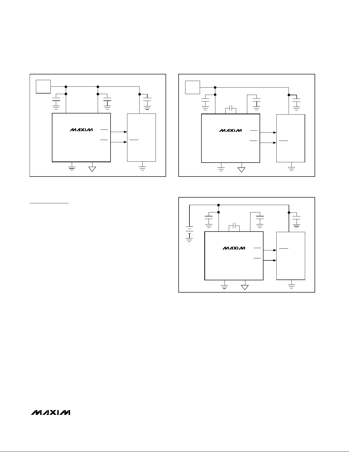
MAX1329/MAX1330
12-/16-Bit DASs with ADC, DACs, DPIOs, APIOs,
Reference, Voltage Monitors, and Temp Sensor
______________________________________________________________________________________ 63
Applications Information
Power-Supply Considerations
The circuit in Figure 23 applies an external 3.0V power
supply to both DVDDand AVDD. To drive AVDDdirectly,
disable the internal charge pump through the CP/VM
Control register. The bypass switch between DV
DD
and
AV
DD
can be either open or closed in this configuration.
Figure 24 shows the charge pump enabled to supply
AV
DD
. The charge-pump output voltage is set to 5.0V
through the CP/VM Control register. See the
Charge-
Pump Component Selection
section.
Figure 25 shows DV
DD
is powered from a battery with
the charge-pump output set to 3.0V. The charge pump
can draw high peak currents from DV
DD
under maximum load. Select an appropriately sized bypass capacitor for DV
DD
(≥ 10 times C
FLY
). Supply ripple can be
reduced by increasing CA
VDD
and/or the charge-pump
clock frequency.
Running Directly Off Batteries
The MAX1329/MAX1330 can be powered directly from
two alkaline cells, two silver oxide button cells, or a lithium-coin cell. DVDDrequires 1.8V to 3.6V and AV
DD
requires 2.7V to 5.5V for proper operation. Save power
by running DVDDdirectly off the battery and shorting to
AVDDby closing the internal bypass switch. Use the
2.7V AVDDvoltage monitor to detect when it drops to
2.7V. Power is saved during this time because the internal charge pump is off. Once the battery voltage drops
to 2.7V, open the bypass switch and enable the internal
charge pump as long as DVDDis between 1.8V and
2.7V. Following this procedure optimizes the battery life.
Digital-Interface Connections
Figure 26 provides standard digital-interface connections
between the MAX1329/MAX1330 and a µC. The µC generates its own 32kHz clock for timekeeping and the
MAX1329/MAX1330 provide the high-frequency clock
required by the µC. See the
Clock Control Register
section to program the CLKIO output and frequency and set
the ODLY bit to delay the turn-off time to enable the µC
time to go to sleep. During sleep, CLKIO becomes an
input and requires a weak pulldown resistor (≤1MΩ) to
minimize power dissipation. See the DPIO Setup and
DPIO Control registers to program DPIO1–DPIO4 as
wake-ups. Upon wake-up, the internal oscillator starts and
outputs to CLKIO. See the
CP/VM Control Register
section to program the RST1 and RST2 as a reset or interrupt.
Figure 23. Power-Supply Circuit Using an External 3.0V Power
Supply for DV
DD
and AV
DD
Figure 24. Power-Supply Circuit Using an External 3.0V Power
Supply for DV
DD
and Internal Charge Pump Set to 5V for AV
DD
Figure 25. Power-Supply Circuit Using a Battery for DVDDand
Internal Charge Pump Set to 3.0V for AV
DD
POWER
SUPPLY
0.1µF
2.7V TO 3.6V
C1A C1B
DV
DD
MAX1329
MAX1330
DGND AGND
0.1µF
AV
DD
RST1
RST2
INTERRUPT
RESET
V
DD
µC
DGND
0.1µF
POWER
SUPPLY
C
DVDD
2.7V TO 3.6V
C
C1A C1B
DV
DD
MAX1329
MAX1330
DGND AGND
5.0V
C
RST1
RST2
AVDD
INTERRUPT
RESET
FLY
AV
DD
V
DD
µC
DGND
0.1µF
C
DVDD
E1
1.8V TO 3.6V
3.0V
C
C
C1A C1B
DV
DD
MAX1329
MAX1330
DGND AGND
FLY
AV
AVDD
DD
RST1
RST2
V
DD
RESET
µC
INTERRUPT
DGND
0.1µF
Page 64

MAX1329/MAX1330
12-/16-Bit DASs with ADC, DACs, DPIOs, APIOs,
Reference, Voltage Monitors, and Temp Sensor
64 ______________________________________________________________________________________
Communication with a Peripheral Device
Powered by the MAX1329/MAX1330
The circuit in Figure 27 shows the MAX1329/MAX1330
providing an interface between a µC and a peripheral
device powered by different supply voltages. This eliminates the need for external level-translation circuitry due
to the different supply voltages. The internal charge
pump boosts the µC supply voltage (DVDD) to the peripheral device supply voltage (AV
DD
). See the APIO Control
and APIO Setup registers to program APIO2–APIO4 as
DIN, SCLK, and CS outputs to the peripheral device,
respectively, and APIO1 as the DOUT input from the
peripheral device. The digital inputs at DIN, SCLK, and
CS are level-translated from DVDDto AVDDand output at
the configured APIO2, APIO3, and APIO4 outputs. The
digital output at DOUT is level-translated from AVDDto
DV
DD
from the configured APIO1 input.
Figure 26. Digital-Interface Connections
Figure 27. Communication with a Peripheral Device Powered by the MAX1329/MAX1330
POWER
SUPPLY
EXTERNAL 1.8V TO 3.6V
C
DVDD
DV
XIN
32.768kHz
MAX1329
MAX1330
CLKIO
CS
SCLK
DOUT
RST1
RST2
DPIO1
DPIO2
XOUT
µC
HCLKIN
OUTPUT
SCK
MOSIDIN
MISO
RESET
INTERRUPT
INTERRUPT
INTERRUPT
3.0V/4.0V/5.0V
C
AVDD
C
FLY
DD
C1A C1B
AV
DD
DV
DD
µC
DGND
OUTPUT
SCK
MOSI
MISO
CS
SCLK
DIN
DOUT
MAX1329
MAX1330
DGND
APIO4
APIO3
APIO2
APIO1
AGND
CS
SCLK
DIN
DOUT
AV
DD
PERIPHERAL
DEVICE
AGND
Page 65

MAX1329/MAX1330
12-/16-Bit DASs with ADC, DACs, DPIOs, APIOs,
Reference, Voltage Monitors, and Temp Sensor
______________________________________________________________________________________ 65
Optical Reflectometry Application with
Dual LED and Single Photodiode
Figure 28 illustrates the MAX1329 in an optical reflectometry application with two transmitting LEDs and one
receiving photodiode. The LEDs transmit light at specific
frequencies onto the sample strip and the photodiode
receives the reflections from the strip. Set the DACA output to provide the appropriate bias currents for the LEDs.
The DSWA and DSWB switches are open in this configuration. The LED bias current is calculated as I
LED
=
V
OUTA/RB
. REFADC is used as an analog ground and
DACB is set to ensure that the photodiode is not forward
biased. The IFcurrent is converted to a voltage through
the RFresistor and measured by the internal ADC.
SPDT1 and SPDT2 are configured as single-pole
double-throw switches and enable switching between
Figure 28. Optical Reflectometry Application with Dual LED and Single Photodiode
REFDAC
DACA
REFDAC
DACB
SPDT1
MAX1329
SPDT2
DSWA
DSWB
OUTA
SNO1
SCM1
SNC1
SNC2
SCM2
SNO2
OUTB
FBA
V
BAT
LED
Q
1
V
BAT
LED
Q
2
R
B
I
R
F
F
FBB
PHOTO
DIODE
= 0.5, 0.82, 1
REF
A
V
A
= 0.5, 0.82, 1
V
REFADC
REFADJ2.5V
REFDAC
1.25V
2.50V
1μF
0.01μF
1μF
Page 66

MAX1329/MAX1330
12-/16-Bit DASs with ADC, DACs, DPIOs, APIOs,
Reference, Voltage Monitors, and Temp Sensor
66 ______________________________________________________________________________________
the two LEDs. The LEDs can be powered directly from
V
BAT
or from AVDDpowered by the internal charge
pump if the VDof the LEDs require a higher or regulated voltage. Ambient light rejection is performed in the
digital domain in this configuration by digitizing the
photodiode current with the internal ADC while both
LEDs are off and subtracting this from the result when
the LEDs are turned on.
Three-Electrode Potentiostat with
Software-Switchable Single- or Dual-
Channel Connection
The MAX1329 is used in a software switchable singleor dual-channel three-electrode potentiostat application
(see Figure 29). In both configurations, the DAC buffer
feedback switches, DSWA and DSWB, are normally
open but can be closed during high sensor current to
keep the DAC buffer outputs compliant. In the dualchannel configuration, the SPDT1 switch is open and
the OSW1 switch is closed. DACA biases the working
electrode (WE) and DACB biases the reference electrode (RE) both relative to the counter electrode (CE).
The CE is shared by the two channels. In this configuration, RE is really a second working electrode and I
A
and IBare the two sensor currents being measured. I
A
and IBare converted to voltages through RAand R
B
and measured by the internal ADC. In the single-channel configuration, the SPDT1 switch is closed and the
OSW1 switch is open. DACA biases the WE relative to
the RE and the RE is set by IN1-. Op amp 1’s forcesense configuration holds RE constant while the CE
swings up and down depending on the sensor current
and the sensor impedance. In this configuration, IAis
the sensor current being measured. The R1resistor is
typically a large value to keep op amp 1 stable when
the sensor is not present or not active.
Two-Electrode Potentiostat with AC and
DC Excitation
The circuit in Figure 30 shows the MAX1330 in a twoelectrode potentiostat application with both AC and DC
excitation to the sensor. The DSWA can be open or
closed and OSW1 and OSW2 should be normally open
although OSW1 can be closed during high sensor
current to keep op amp 1 in compliance. REFADC is
analog ground and the working electrode (WE) is connected to analog ground through op amp 1. The sensor
current to be measured is converted to a voltage
through RFand measured by the internal ADC. For DC
operation, the bias voltage between WE and the
counter electrode (CE) is set by DACA. For AC operation, DACA is configured to generate a waveform by
programming the FIFOA Control and FIFOA Data registers for the desired operation. Op amp 2 is configured
as a 2nd-order Sallen Key lowpass filter to smooth the
steps in the AC waveform going to the sensor. The
DACA can be sequenced to create an AC waveform
through the SPI interface or by configuring one of the
DPIOs and driving it with a clock. The internal ADC
includes a 16-word FIFO to facilitate data gathering
during this mode of operation.
Temperature Measurement with Two
Remote Sensors
For external measurements, select single-ended AIN1
and AIN2 temperature measurement relative to AGND
in the lower multiplexer. Two diode-connected 2N3904
transistors are used as external temperature sensing
diodes in Figure 31. For internal temperature sensor
measurements, select internal temperature measurement in the lower multiplexer. During all temperature
measurements, autoconvert and burst modes are
unavailable. Divide the ADC result by eight to obtain
the measured temperature.
When using an external reference at REFADJ, disable the
internal reference and use the temperature correction
equation in the
Temperature Measurement
section.
Page 67

MAX1329/MAX1330
12-/16-Bit DASs with ADC, DACs, DPIOs, APIOs,
Reference, Voltage Monitors, and Temp Sensor
______________________________________________________________________________________ 67
Figure 29. Three-Electrode Potentiostat Software-Switchable Single- or Dual-Channel Connection
REFDAC
DACA
REFDAC
DACB
MAX1329
SPDT1
DSWA
DSWB
OSW1
OUTA
OUTB
FBA
FBB
SNO1
SCM1
SNC1
IN1-
I
A
R
A
R
B
I
B
WE
RE
CE
R
1
OA1
OUT1
2.5V
REF
A
= 0.5, 0.82, 1
V
A
= 0.5, 0.82, 1
V
REFADC
REFADJ
REFDAC
IN1+
2.50V
1.25V
1μF
0.01μF
1μF
Page 68
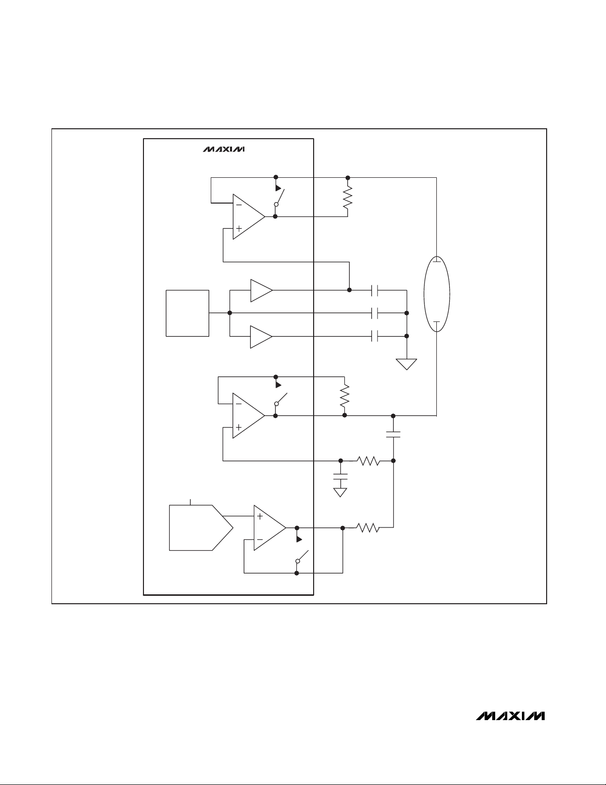
MAX1329/MAX1330
12-/16-Bit DASs with ADC, DACs, DPIOs, APIOs,
Reference, Voltage Monitors, and Temp Sensor
68 ______________________________________________________________________________________
Figure 30. Two-Electrode Potentiostat with AC and DC Excitation
MAX1330
IN1-
= 0.5, 0.82, 1
A
V
2.5V
REF
= 0.5, 0.82, 1
A
V
OSW1
OA1
OA2
OSW2
OUT1
OUT2
IN1+
REFADC
REFADJ
REFDAC
IN2-
IN2+
2.50V
R
C2
R
F
1.25V
3
1μF
0.1μF
1μF
R
2
WE
CE
SENSOR
C1
REFDAC
R
DACA
OUTA
DSWA
FBA
1
Page 69

MAX1329/MAX1330
12-/16-Bit DASs with ADC, DACs, DPIOs, APIOs,
Reference, Voltage Monitors, and Temp Sensor
______________________________________________________________________________________ 69
Figure 31. Temperature Measurement with Two Remote Sensors
Programmable-Gain Instrumentation
Amplifier
Two op amps and two SPDT switches are configured
as a programmable-gain instrumentation amplifier in
Figure 32. It includes a differential input and a singleended output. SPDT1 and SPDT2 are configured as
single-pole, double-throw switches. The gain is set by
the following equations:
for switch position 1, and
for switch position 2.
AIN1
AIN2
OUTA/OUT3
FBA/IN3-
OUT1
IN1-
OUTB/OUT2
FBB/IN2-
TEMP1
TEMP2
TEMP3
DV
DD
AV
DD
REFADC
REFDAC
AGND
AND C
AIN1
/4
/4
AIN2
TO 10pF.
2N3904
2N3904
AIN1
C
*
AIN1
AGND
AIN2
*
C
AIN2
AGND
*FOR BEST RESULTS, LIMIT C
MAX1329
MAX1330
MUX
MUX
TEMP
SENSOR
PGA
AV = 1, 2, 4, 8
TEMP1
ACCUMULATOR
AV = 0.5, 0.82, 1
2.5V
REF
AV = 0.5, 0.82, 1
12-BIT ADC
DITHER
ALARM
ADC FIFO
REFADC
REFADC
REFADJ
REFDAC
1μF
0.01μF
1μF
V
V
OUT IN IN
⎛
RR
+
23
=
OUT IN IN
⎜
R
⎝
⎛
R
3
=
⎜
RR
+
⎝
12
⎞
+
1( )
⎟
⎠
1
⎞
VV
+
1( )
⎟
⎠
VV
−
+ −
−
+ −
Page 70

MAX1329/MAX1330
12-/16-Bit DASs with ADC, DACs, DPIOs, APIOs,
Reference, Voltage Monitors, and Temp Sensor
70 ______________________________________________________________________________________
Synthesizing a Sine Wave
The MAX1329/MAX1330 can easily create up to a
64-point single or periodic sine wave using the DACA
and FIFOA. The 16-word FIFO or memory is used to
create the first quarter of the waveform and symmetry is
used to extend the waveform to produce a complete
period. See the
DAC FIFO and Direct Digital Synthesis
(DDS) Logic
section for detailed waveform generation.
The first data point is the DACA input register data. The
FIFOA data is offset from this initial data. To determine
the values to be written to the FIFOA Data register use
the following equation.
FIFOA_DATA(n) = A x sin((n/N) x 90°)
where
n = 1 to N,
N = DPTA<3:0>,
A = (V
PEAK/VREFDAC
) x 4096,
V
PEAK
is the desired peak voltage of the sine wave,
and V
REFDAC
is the DAC reference voltage pro-
grammed at REFDAC.
Round the FIFOA_DATA(n) values to the nearest integer and write these values to the FIFOA Data register.
Figure 33 shows a sine wave with a 2V
P-P
output and
with a 1.25V offset. Write the DAC Control register with
0x43 to enable DACA, enable the internal reference,
and to set REFDAC to 2.5V. Write to the DACA input
and output register by performing a direct mode write
with 0x4800 to set DACA to midscale or 1.25V. Write
the FIFOA Control register with 0x7F to disable FIFOA
and allow a write to the FIFOA Data register, enabling
bipolar, symmetry, and continuous modes, and setting
the depth to 16.
The FIFOA data calculated from the above equation is
161, 320, 476, 627, 772, 910, 1039, 1159, 1267, 1362,
1445, 1514, 1568, 1607, 1631, and 1638 decimal. Write
the FIFOA Data register with 0x0A10 1400 1DC0 2730
3040 38E0 40F0 4870 4F30 5520 5A50 5EA0 6200
6470 65F0 6660 as a contiguous bit stream to fill the
FIFOA Data register with data. Write to the FIFOA
Control register with 0xFF to enable FIFOA and to disallow writes to the FIFOA Data register. Write to the DPIO
Control register with 0x0007 to program DPIO1 as an
input to sequence the DACA FIFO on each rising edge.
Write to the Switch Control register with 0x80 to close
the DACA switch to put the buffer into unity gain. Input
a continuous clock to DPIO1 that is 4 x N times (N = 16)
the desired frequency of the synthesized waveform.
Figure 33 should be observable on OUTA.
Figure 32. Programmable-Gain Instrumentation Amplifier,
Switch Position 1
Figure 33. Example Sine-Wave Output
IN1+
V
IN+
IN1-
SCM1
IN2+
V
IN-
IN2-
SCM2
OA1
OSW1
SPDT1
OA2
OSW2
SPDT2
MAX1330
OUT1
SNO1
SNC1
OUT2
SNO2
SNC2
R
3
R
2
R
1
R
1
R
2
R
3
V
OUT
SINE WAVE
2.50
2.25
2.00
1.75
1.50
1.25
1.00
DAC OUTPUT (V)
0.75
0.50
0.25
0
0 10203040506070
DAC SEQUENCES
Page 71
MAX1329/MAX1330
12-/16-Bit DASs with ADC, DACs, DPIOs, APIOs,
Reference, Voltage Monitors, and Temp Sensor
______________________________________________________________________________________ 71
Charge-Pump Component Selection
Optimize the charge-pump circuit for size, quiescent
current, and output ripple by properly selecting the
operating frequency and capacitors C
DVDD
, C
FLY
, and
C
AVDD
(Table 32). The charge pump is capable of providing a maximum of 25mA including what is used
internally. If less than 25mA is required, smaller capacitor values can be utilized.
For lowest ripple, select 117kHz operation (CPDIV<1:0>
= 00 and OSCE = 1 when using the internal oscillator). In
addition, increasing C
AVDD
relative to C
FLY
further
reduces ripple. For highest efficiency, select 14.6kHz
operation (CPDIV<1:0> = 11 and OSCE = 1 when using
the internal oscillator) and select the largest practical
values for C
AVDD
and C
FLY
while maintaining at least a
30-to-1 ratio. For smallest size, select 117kHz operation.
See Table 32 for some suggested values and resulting
ripple for 25mA load current. See Figure 34 for load current vs. flying capacitor value when optimizing for other
load currents.
Note that the capacitors must have low ESR to maintain low ripple. The C
FLY
flying capacitor ESR needs
to be < 0.1Ω; and the C
AVDD
and C
DVDD
filter capaci-
tor ESR needs to be < 0.3Ω. The C
FLY
flying capacitor
can easily be a ceramic capacitor; and the C
AVDD
and
C
DVDD
filter capacitor can be a low-ESR tantalum or
may need to be a combination of a small ceramic and a
larger tantalum capacitor.
When DVDDis lower than AVDD, the charge pump always
operates in voltage-doubler mode. It regulates the output
voltage using a pulse-width-modulation (PWM) scheme.
Using a PWM scheme ensures that the charge pump is
synchronous with the internal ADC preventing corruption
of the conversion results.
Operating the Analog Switches
The MAX1329/MAX1330 include two single-pole doublethrow (SPDT) and three single-pole single-throw (SPST)
analog switches. The two SPDT analog switches are
uncommitted and the three SPST analog switches are
connected between the DAC buffer or op amp outputs
and the inverting inputs.
The analog switches can be controlled using the Switch
Control register or any of the DPIOs. See the DPIO
Control and DPIO Setup registers to program the
DPIOs. The DPIOs should be used when direct control
is critical such as synchronizing with another event or if
the SPI bus bandwidth is not sufficient for the intended
application. The register bit for the analog switch is logically OR’d with DPIOs enabled to control that switch.
The SPDT1 and SPDT2 analog switches can be operated as a SPDT or as a double-pole single-throw (DPST).
In the DPST mode, both switches can be opened or
closed together. This is useful when connecting two
external nodes to a common point. If a lower on-resistance is required, NO_ and NC_ can be connected
together externally and be used as a SPST analog
switch with half the on-resistance.
The SPST analog switches are intended to be used to
set the DAC buffers and op amps to unity gain internally by software control. When the DAC buffers and op
amps are used as transimpedance amplifiers, the SPST
analog switches can be used to short the external transimpedance resistor during high current periods to
keep the amplifier output in compliance.
Table 32. External Component Selection
for 25mA Output Current and 2V
DVDD
-
V
AVDD
≥ 0.4V (Figure 25)
Figure 34. Load Current vs. CFLY Value for 2V
DVDD
- V
AVDD
≥
0.4V
CHARGE-PUMP
CLOCK (kHz)
I
LOAD,
MAX
(mA)
14.4
28.8
57.6
115.2
25 1.7 55.6 17.4
12.5 0.9 27.8 8.7
25 0.9 27.8 8.7
12.5 0.4 13.9 4.3
25 0.4 13.9 4.3
12.5 0.2 6.9 2.2
25 0.2 6.9 2.2
12.5 0.1 3.5 1.1
C
FLY
(µF)
C
AVDD
(µF)
C
DVDD
(µF)
RIPPLE
(mV)
32
32
32
32
CHARGE-PUMP LOAD CURRENT
vs. FLYING CAPACITOR VALUE
50
45
40
35
30
25
LOAD (mA)
I
20
15
10
5
0
05.0
fCP = 115.2kHz
fCP = 57.6kHz
fCP = 28.8kHz
C
(µF)
FLY
fCP = 14.4kHz
4.54.03.0 3.51.0 1.5 2.0 2.50.5
MAX1329 fig34
Page 72

MAX1329/MAX1330
12-/16-Bit DASs with ADC, DACs, DPIOs, APIOs,
Reference, Voltage Monitors, and Temp Sensor
72 ______________________________________________________________________________________
Using the Internal Reference and
Reference Buffers
The MAX1329/MAX1330 include a precision 2.5V internal
reference and two independent programmable buffers for
the ADC and DACs. See the ADC Control and DAC
Control registers to enable the internal reference and program the buffers. The REFADJ output is fixed at 2.5V
(REFE = 1) and the REFADC and REFDAC connect to the
internal ADC reference input and the internal DAC reference inputs, respectively. These buffers can be programmed to output 1.25V, 2.048V, or 2.5V independent
of each other. This allows the dynamic range of the ADC
and DACs to be optimized or set differently. This is useful
if one of the reference voltages is needed to be approximately AV
DD
/2 to be used as an analog ground.
The flexibility of the reference circuit allows the internal
reference to be shutdown (REFE = 0) and an external
voltage reference applied to REFADJ. If either REFADC
or REFDAC requires a different or more accurate voltage, an external reference can be applied directly to
REFADC or REFDAC and the corresponding reference
buffer must be disabled.
Applying a Digital Filter to ADC Data Using
the 20-Bit Accumulator
The MAX1329/MAX1330 incorporate a 20-bit accumulator that can sum up to 256 results of the 12-bit ADC
automatically. See the
ADC Accumulator Register
section to set the number of samples to be summed. Once
the accumulator is full, the ACF bit in the Status register
is asserted.
The accumulator provides a digital filtering sync function, with an effective data rate equal to f
EDR
= fS/n
where fSis the ADC sample rate and n is the number of
samples accumulated. There is a notch at every integer
multiple of f
EDR
. The following equation provides the
transfer function of the filter:
Figure 35 is a plot showing a notch at 60Hz by accumulating 256 samples at 15.36ksps.
The final step is to read the data in the ADC Accumulator
register and divide by the number of samples that were
accumulated. Shift the data right for each binary multiple of accumulated data. For example, for 256 samples
the data should be shifted right eight times.
Increasing ADC Resolution using the
Accumulator with Dither
The MAX1329/MAX1330 incorporate an internal dither
function that can be used along with the 20-bit accumulator to easily increase the resolution of the 12-bit ADC
to up to 16 bits. The oversampling along with the dither
increases the resolution with the penalty of a lower
effective data rate. Use the following equation to determine the number of samples required to increase the
resolution by N number of bits:
Samples = 2
2N
To increase the resolution by 4 bits, from 12 to 16 bits,
256 samples are required. After accumulating the
required number of samples, read the data from the
ADC Accumulator register and shift right by 4 bits with
the 16 LSBs as the increased resolution result.
Figure 35. Plot of the Digital Filter with 60Hz Notch
Hf
()
⎛
⎞
nf
π
sin
⎜
⎟
⎝
⎛
nf
⎜
⎝
f
⎠
s
⎞
π
⎟
f
⎠
s
⎛
⎞
nf
π
c
sin=
=
⎜
⎟
f
⎝
⎠
s
DIGITAL-FILTER TRANSFER FUNCTION
0
-5
-10
-15
-20
-25
-30
-35
FILTER RESPONSE (dB)
-40
-45
-50
0 120 18060 240 300 360 420 480
FREQUENCY (Hz)
Page 73

MAX1329/MAX1330
12-/16-Bit DASs with ADC, DACs, DPIOs, APIOs,
Reference, Voltage Monitors, and Temp Sensor
______________________________________________________________________________________ 73
Using the ADC with the ADC LT
(Less-Than) and GT (Greater-Than)
Digital Alarms
The ADC LT and GT alarms compare the latest ADC
result to the values programmed in the ADC LT Alarm
and ADC GT Alarm registers, if enabled, and assert the
appropriate GTA or LTA status bit in the Status register
once the threshold has been exceeded. The digital
alarms can be used as a safeguard during normal ADC
conversions to signify an event. Change the GT and LT
alarm thresholds, if needed, when selecting a new mux
input channel. The ADC can be put into autoconversion
mode to continuously convert without user intervention.
See the AUTO<2:0> bits in the
ADC Control Register
section to enable the auto mode and to program the
ADC conversion rate.
Layout, Grounding, and Bypassing
For best performance, use PCBs. Do not use wire-wrap
boards. Board layout should ensure that digital and analog signal lines are separated from each other. Do not run
analog and digital (especially clock) signals parallel to
one another or run digital lines underneath the
MAX1329/MAX1330 package. High-frequency noise in
the VDDpower supply can affect the MAX1329/MAX1330
performance. Bypass the AV
DD
and DVDDsupplies with
a 0.1µF capacitor to GND, close to the AV
DD
and DV
DD
pins (see Table 32 for recommended capacitor values).
Minimize capacitor lead lengths for best supply-noise
rejection.
Selector Guide
+
Denotes a lead-free/RoHS-compliant package.
PART NO. OF DACS NO. OF OP AMPS
MAX1329BETL+ 2 1 ±3 ±75 -40°C to +85°C
MAX1330BETL+ 1 2 ±3 ±75 -40°C to +85°C
TEMP SENSOR
ACCURACY (°C)
INTERNAL
REFERENCE TEMP
COEFFICIENT
(ppm/°C max)
TEMP
RANGE
Page 74
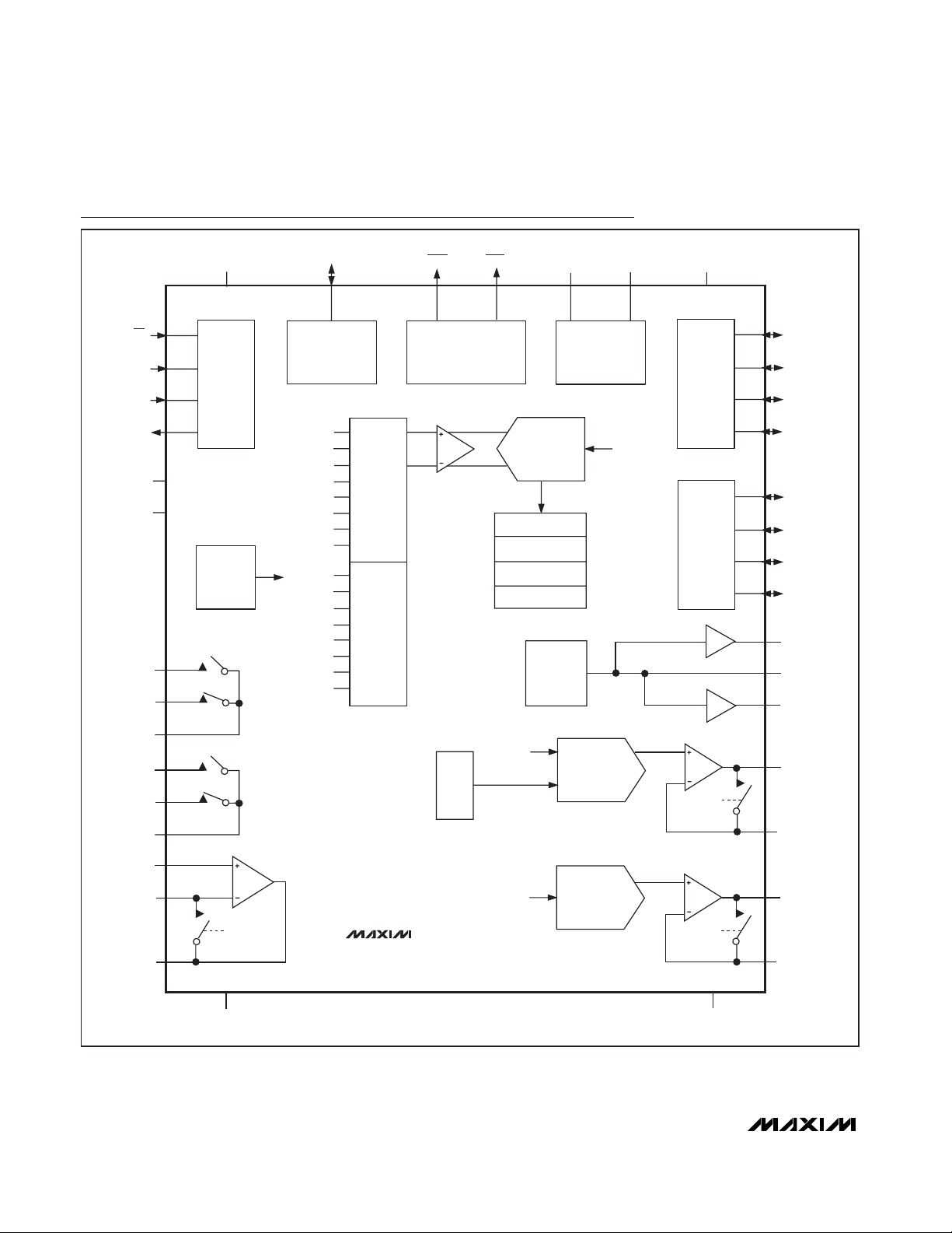
MAX1329/MAX1330
12-/16-Bit DASs with ADC, DACs, DPIOs, APIOs,
Reference, Voltage Monitors, and Temp Sensor
74 ______________________________________________________________________________________
Functional Diagrams
DV
DD
CLKIO
RST1
RST2
C1A
C1B
AV
DD
CS
SCLK
DIN
DOUT
AIN1
AIN2
SERIAL
I/O
TEMP
SENSOR
SNO1
SNC1
SCM1
SNO2
SNC2
SPDT1
SPDT2
INTERNAL
CLOCK AND
AIN1
AIN2
OUTA
FBA
OUT1
IN1-
OUTB
FBB
TEMP1
TEMP2
TEMP3
DV
DD
AV
DD
REFADC
REFDAC
AGND
DIVIDER
/4
/4
UPPER
LOWER
MUX
MUX
VOLTAGE
SUPERVISORS AND
INTERRUPTS
PGA
= 1, 2, 4, 8
A
V
REFDAC
DACA
FIFO
12-BIT ADC
DITHER
ACCUMULATOR
ALARM
ADC FIFO
2.50V
BANDGAP
CHARGE
PUMP
12-BIT
DACA
REFADC
= 0.5, 0.8192, 1.0
A
V
A
= 0.5, 0.8192, 1.0
V
DPIO1
DPIO2
DPIO
DPIO3
DPIO4
APIO1
APIO2
APIO
APIO3
APIO4
REFADC
REFADJ
REFDAC
OUTA
DSWA
SCM2
IN1+
IN1-
OUT1
DGND
OSW1
OA1
MAX1329
REFDAC
12-BIT
DACB
DSWB
AGND
FBA
OUTB
FBB
Page 75

MAX1329/MAX1330
12-/16-Bit DASs with ADC, DACs, DPIOs, APIOs,
Reference, Voltage Monitors, and Temp Sensor
______________________________________________________________________________________ 75
Functional Diagrams (continued)
CS
SCLK
DIN
DOUT
AIN1
AIN2
SNO1
SNC1
SCM1
SNO2
SNC2
DV
DD
SERIAL
I/O
TEMP
SENSOR
SPDT1
SPDT2
INTERNAL
CLOCK AND
AIN1
AIN2
OUTA
FBA
OUT1
IN1-
OUT2
IN2-
TEMP1
TEMP2
TEMP3
DV
DD
AV
DD
REFADC
REFDAC
AGND
CLKIO
DIVIDER
/4
/4
UPPER
MUX
LOWER
MUX
VOLTAGE
INTERRUPTS
PGA
= 1, 2, 4, 8
A
V
DACA
FIFO
RST2
REFDAC
RST1
SUPERVISORS AND
AV
DPIO
APIO
DSWA
DD
DPIO1
DPIO2
DPIO3
DPIO4
APIO1
APIO2
APIO3
APIO4
REFADC
REFADJ
REFDAC
OUTA
12-BIT ADC
DITHER
ACCUMULATOR
ALARM
ADC FIFO
2.50V
BANDGAP
C1A
CHARGE
PUMP
12-BIT
DACA
C1B
REFADC
= 0.5, 0.8192, 1.0
A
V
A
= 0.5, 0.8192, 1.0
V
SCM2
IN1+
IN1-
OUT1
FBA
OA1
OUT2
IN2-
DGND
OSW1
MAX1330
IN2+
OA2
OSW2
AGND
Page 76

MAX1329/MAX1330
12-/16-Bit DASs with ADC, DACs, DPIOs, APIOs,
Reference, Voltage Monitors, and Temp Sensor
76 ______________________________________________________________________________________
Typical Operating Circuit
1.8V TO 3.6V
E1
10µF
0.1µF
1µF
3.0V
33µF
0.1µF
AIN1
2N3904
0.01µF
R
F
WE
SENSOR
RE
CE
AIN2
1µF
REFADC
REFADJ
REFDAC
1µF
OUTA
FBA
FBB
OUTB
C1B
C1ADV
DD
MAX1329
AGND DGND
AV
DD
32.768kHz
CLKIO
SCLK
DIN
DOUT
RST2
DPIO1
DPIO2
V
XIN
XOUT
HCLKIN
µC
OUTPUTCS
SCK
MOSI
MISO
RESETRST1
INTERRUPT
INTERRUPT
INTERRUPT
DGND
DD
Page 77
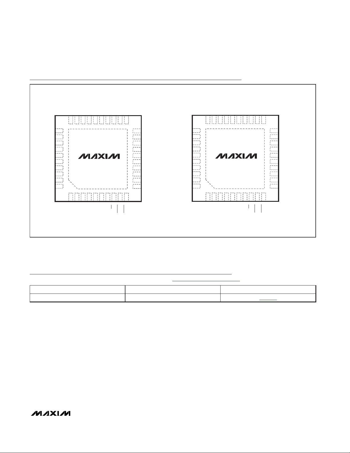
MAX1329/MAX1330
12-/16-Bit DASs with ADC, DACs, DPIOs, APIOs,
Reference, Voltage Monitors, and Temp Sensor
______________________________________________________________________________________ 77
Pin Configurations
PACKAGE TYPE PACKAGE CODE DOCUMENT NO.
40 TQFN-EP T4066-5
21-0141
Package Information
For the latest package outline information and land patterns, go to www.maxim-ic.com/packages.
TOP VIEW
AIN1
REFADC
REFADJ
AGND
AV
DD
C1B
C1A
DV
DD
DGND
CLKIO
AIN2
SNO2
SNC2
REFDAC
SCM2
30 29 28 27 26 25 24 23 22 21
31
32
33
34
35
36
37
38
39
40
+
1 2 3 4 5 6 7 8 9 10
DPIO1
MAX1329
EXPOSED PAD—
CONNECT TO AGND
DOUT
DPIO3
DPIO4
DPIO2
SCLK
THIN QFN
FBA
OUTA
DIN
OUTB
CS
FBB
RST1
N.C.
RST2
TOP VIEW
AIN2
SNO2
SNC2
REFDAC
SCM2
30 29 28 27 26 25 24 23 22 21
31
20
OUT1
IN1-
19
18
IN1+
17
SNC1
16
SCM1
15
SNO1
14
APIO4
13
APIO3
12
APIO2
11
APIO1
AIN1
REFADC
REFADJ
AGND
AV
C1B
C1A
DV
DGND
CLKIO
32
33
34
35
DD
36
37
38
DD
39
40
+
1 2 3 4 5 6 7 8 9 10
DPIO1
MAX1330
EXPOSED PAD—
CONNECT TO AGND
DOUT
DPIO3
DPIO4
DPIO2
FBA
SCLK
OUTA
DIN
OUT2
CS
IN2-
RST1
IN2+
RST2
20
OUT1
IN1-
19
18
IN1+
17
SNC1
16
SCM1
15
SNO1
14
APIO4
13
APIO3
12
APIO2
11
APIO1
THIN QFN
Page 78

MAX1329/MAX1330
12-/16-Bit DASs with ADC, DACs, DPIOs, APIOs,
Reference, Voltage Monitors, and Temp Sensor
Maxim cannot assume responsibility for use of any circuitry other than circuitry entirely embodied in a Maxim product. No circuit patent licenses are
implied. Maxim reserves the right to change the circuitry and specifications without notice at any time.
78
____________________Maxim Integrated Products, 120 San Gabriel Drive, Sunnyvale, CA 94086 408-737-7600
© 2008 Maxim Integrated Products is a registered trademark of Maxim Integrated Products, Inc.
Revision History
REVISION
NUMBER
0 8/08 Initial release —
1 10/08 Corrected Absolute Maximum Ratings table 2
REVISION
DATE
DESCRIPTION
PAGES
CHANGED
 Loading...