

Page 1
General Description
The MAX1316–MAX1318/MAX1320–MAX1322/MAX1324–
MAX1326 14-bit, analog-to-digital converters (ADCs) offer
two, four, or eight independent input channels.
Independent track/hold (T/H) circuitry provides simultaneous sampling for each channel. The MAX1316/
MAX1317/MAX1318 have a 0 to +5V input range with
±6.0V fault-tolerant inputs. The MAX1320/MAX1321/
MAX1322 have a ±5V input range with ±16.5V fault-tolerant inputs. The MAX1324/MAX1325/MAX1326 have a
±10V input range with ±16.5V fault-tolerant inputs. These
ADCs convert two channels in 2µs, and up to eight channels in 3.8µs, and have an 8-channel throughput of
250ksps per channel. Other features include a 10MHz
T/H input bandwidth, internal clock, internal (+2.5V) or
external (+2.0V to +3.0V) reference, and powersaving modes.
A 16.6MHz, 14-bit, bidirectional, parallel interface provides the conversion results and accepts digital configuration inputs.
These devices operate from a +4.75V to +5.25V analog
supply and a separate +2.7V to +5.25V digital supply,
and consume less than 50mA total supply current.
These devices come in a 48-pin TQFP package and operate over the extended -40°C to +85°C temperature range.
Applications
Multiphase Motor Control
Power-Grid Synchronization
Power-Factor Monitoring and Correction
Vibration and Waveform Analysis
Features
♦ 8-/4-/2-Channel, 14-Bit ADCs
±1.5 LSB INL, ±1 LSB DNL, No Missing Codes
90dBc SFDR, -86dBc THD, 76.5dB SINAD, 77dB
SNR at 100kHz Input
♦ On-Chip T/H Circuit for Each Channel
10ns Aperture Delay
50ps Channel-to-Channel T/H Matching
♦ Fast Conversion Time
One Channel in 1.6µs
Two Channels in 1.9µs
Four Channels in 2.5µs
Eight Channels in 3.7µs
♦ High Throughput
526ksps/ch for One Channel
455ksps/ch for Two Channels
357ksps/ch for Four Channels
250ksps/ch for Eight Channels
♦ Flexible Input Ranges
0 to +5V (MAX1316/MAX1317/MAX1318)
±5V (MAX1320/MAX1321/MAX1322)
±10V (MAX1324/MAX1325/MAX1326)
♦ No Calibration Needed
♦ 14-Bit, High-Speed, Parallel Interface
♦ Internal or External Clock
♦ +2.5V Internal Reference or +2.0V to +3.0V
External Reference
♦ +5V Analog Supply, +3V to +5V Digital Supply
46mA Analog Supply Current (typ)
1.6mA Digital Supply Current (max)
Shutdown and Power-Saving Modes
♦ 48-Pin TQFP Package (7mm ✕ 7mm Footprint)
MAX1316–MAX1318/MAX1320–MAX1322/MAX1324–MAX1326
8-/4-/2-Channel, 14-Bit, Simultaneous-Sampling ADCs
with ±10V, ±5V, and 0 to +5V Analog Input Ranges
________________________________________________________________ Maxim Integrated Products 1
Ordering Information
Selector Guide
19-3157; Rev 2; 8/04
For pricing, delivery, and ordering information, please contact Maxim/Dallas Direct! at
1-888-629-4642, or visit Maxim’s website at www.maxim-ic.com.
Pin Configurations and Typical Operating Circuits appear at
end of data sheet.
*Future product—contact factory for availability.
PART TEMP RANGE PIN-PACKAGE
MAX1316ECM -40°C to +85°C 48 TQFP
MAX1317ECM -40°C to +85°C 48 TQFP
MAX1318ECM -40°C to +85°C 48 TQFP
MAX1320ECM -40°C to +85°C 48 TQFP
MAX1321ECM -40°C to +85°C 48 TQFP
MAX1322ECM -40°C to +85°C 48 TQFP
MAX1324ECM -40°C to +85°C 48 TQFP
MAX1325ECM -40°C to +85°C 48 TQFP
MAX1326ECM -40°C to +85°C 48 TQFP
PART INPUT RANGE (V) CHANNEL COUNT
MAX1316ECM 0 to +5 8
MAX1317ECM 0 to +5 4
MAX1318ECM 0 to +5 2
MAX1320ECM ±5 8
MAX1321ECM ±5 4
MAX1322ECM ±5 2
MAX1324ECM ±10 8
MAX1325ECM ±10 4
MAX1326ECM ±10 2
Page 2
MAX1316–MAX1318/MAX1320–MAX1322/MAX1324–MAX1326
8-/4-/2-Channel, 14-Bit, Simultaneous-Sampling ADCs
with ±10V, ±5V, and 0 to +5V Analog Input Ranges
2 _______________________________________________________________________________________
ABSOLUTE MAXIMUM RATINGS
ELECTRICAL CHARACTERISTICS
(AVDD= +5V, DVDD= +3V, AGND = DGND = 0V, V
REF
= V
REFMS
= +2.5V (external reference), C
REF
= C
REFMS
= 0.1µF, C
REF+
=
C
REF-
= 0.1µF, C
REF+-to-REF-
= 2.2µF || 0.1µF, C
COM
= 2.2µF || 0.1µF, C
MSV
= 2.2µF || 0.1µF (unipolar devices, MAX1316/
MAX1317/MAX1318), MSV = AGND (bipolar devices, MAX1320/MAX1321/MAX1322/MAX1324/MAX1325/MAX1326), f
CLK
= 10MHz,
50% duty cycle, INTCLK/
EXTCLK = AGND (external clock), SHDN = DGND, TA = T
MIN
to T
MAX
, unless otherwise noted. Typical val-
ues are at T
A
= +25°C.)
Stresses beyond those listed under “Absolute Maximum Ratings” may cause permanent damage to the device. These are stress ratings only, and functional
operation of the device at these or any other conditions beyond those indicated in the operational sections of the specifications is not implied. Exposure to
absolute maximum rating conditions for extended periods may affect device reliability.
AV
DD
to AGND.........................................................-0.3V to +6V
DV
DD
to DGND.........................................................-0.3V to +6V
AGND to DGND.....................................................-0.3V to +0.3V
CH0–CH7, I.C. to AGND (MAX1316/MAX1317/MAX1318)...±6.0V
CH0–CH7, I.C. to AGND (MAX1320/MAX1321/MAX1322).±16.5V
CH0–CH7, I.C. to AGND (MAX1324/MAX1325/MAX1326).±16.5V
INTCLK/EXTCLK to AGND.......................-0.3V to (AV
DD
+ 0.3V)
EOC, EOLC, WR, RD, CS to DGND.........-0.3V to (DV
DD
+ 0.3V)
CONVST, CLK, SHDN,
ALLON to DGND..................................-0.3V to (DV
DD
+ 0.3V)
MSV, REF
MS
, REF to AGND.....................-0.3V to (AV
DD
+ 0.3V)
REF+, COM, REF- to AGND.....................-0.3V to (AV
DD
+ 0.3V)
D0–D13 to DGND ....................................-0.3V to (DV
DD
+ 0.3V)
Maximum Current into Any Pin Except AV
DD
, DVDD,
AGND, DGND...............................................................±50mA
Continuous Power Dissipation
TQFP (derate 22.7mW/°C above +70°C)...................1818mW
Operating Temperature Range ...........................-40°C to +85°C
Junction Temperature......................................................+150°C
Storage Temperature Range.............................-65°C to +150°C
Lead Temperature (soldering, 10s).................................+300°C
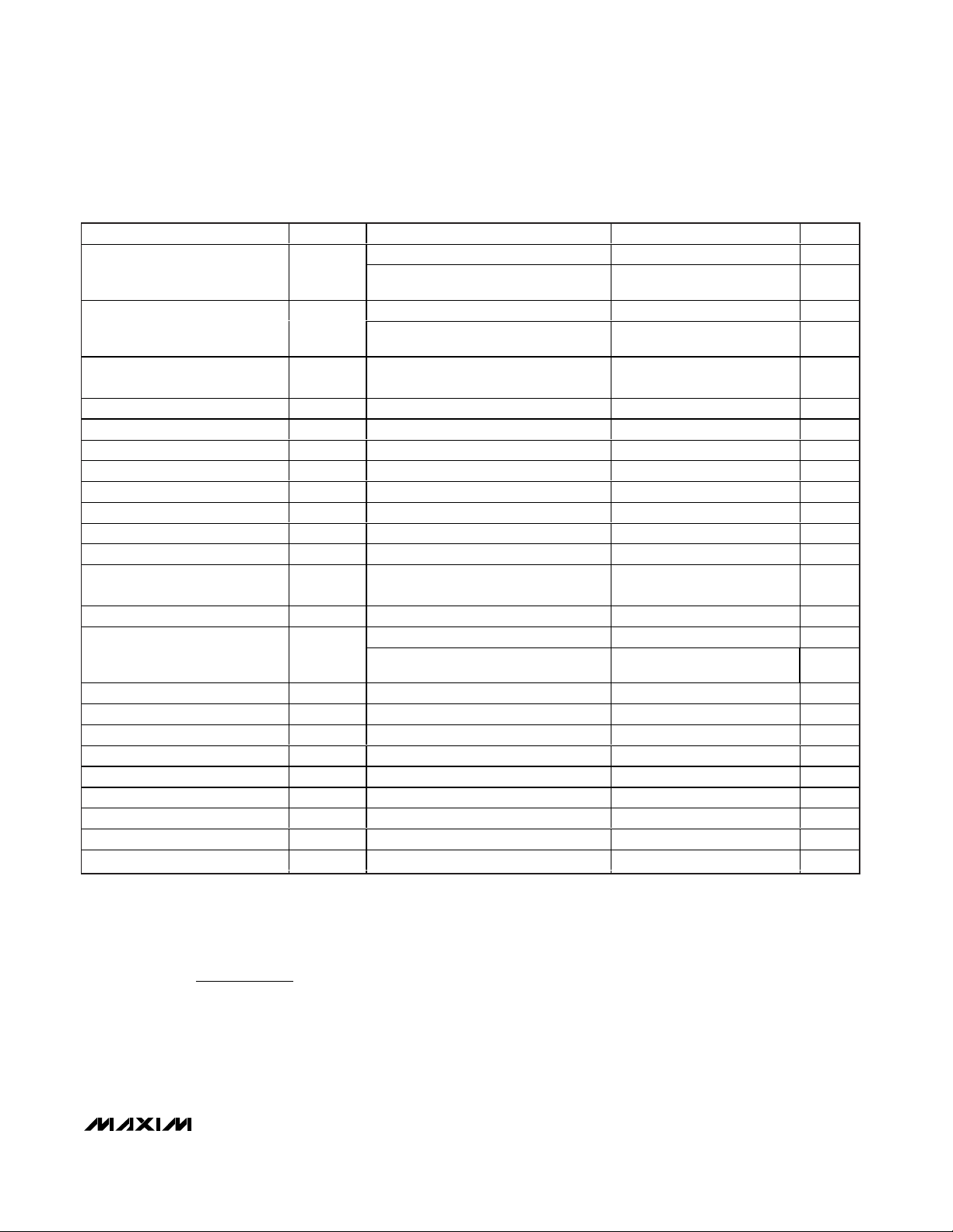
PARAMETER
CONDITIONS
UNITS
STATIC PERFORMANCE (Note 1)
Resolution N 14 Bits
Integral Nonlinearity INL (Note 2)
LSB
Differential Nonlinearity DNL No missing codes (Note 2)
±1 LSB
Unipolar devices
Offset Error
Bipolar devices
LSB
Unipolar devices -4
Offset Drift
Bipolar devices -4
ppm/°C
Unipolar devices between all channels 35 80
Channel Offset Matching
Bipolar devices between all channels 25 60
LSB
Gain Error (Note 3) ±8
LSB
Channel Gain-Error Matching Between all channels 25 LSB
Gain Temperature Coefficient 3
ppm/°C
DYNAMIC PERFORMANCE (at fIN = 100kHz, -0.4dB FS)
Unipolar
76
Signal-to-Noise Ratio SNR
Bipolar 75
dB
Unipolar
76
Signal-to-Noise and Distortion
Ratio
SINAD
Bipolar 75
dB
Spurious-Free Dynamic Range SFDR 83 93 dBc
Total Harmonic Distortion THD -90 -83 dBc
Channel-to-Channel Isolation 83 dB
ANALOG INPUTS (CH0–CH7)
MAX1316/MAX1317/MAX1318 0 +5
MAX1320/MAX1321/MAX1322 -5 +5
Input Voltage Range
MAX1324/MAX1325/MAX1326 -10
V
SYMBOL
MIN TYP MAX
±0.8 ±2.0
±0.5
±40
74.5
76.5
74.5
76.5
±40
±40
+10
Page 3
MAX1316–MAX1318/MAX1320–MAX1322/MAX1324–MAX1326
8-/4-/2-Channel, 14-Bit, Simultaneous-Sampling ADCs
with ±10V, ±5V, and 0 to +5V Analog Input Ranges
_______________________________________________________________________________________ 3
ELECTRICAL CHARACTERISTICS (continued)
(AVDD= +5V, DVDD= +3V, AGND = DGND = 0V, V
REF
= V
REFMS
= +2.5V (external reference), C
REF
= C
REFMS
= 0.1µF, C
REF+
=
C
REF-
= 0.1µF, C
REF+-to-REF-
= 2.2µF || 0.1µF, C
COM
= 2.2µF || 0.1µF, C
MSV
= 2.2µF || 0.1µF (unipolar devices, MAX1316/
MAX1317/MAX1318), MSV = AGND (bipolar devices, MAX1320/MAX1321/MAX1322/MAX1324/MAX1325/MAX1326), f
CLK
= 10MHz,
50% duty cycle, INTCLK/EXTCLK = AGND (external clock), SHDN = DGND, T
A
= T
MIN
to T
MAX
, unless otherwise noted. Typical val-
ues are at T
A
= +25°C.)
PARAMETER
SYMBOL
CONDITIONS
MIN
TYP
MAX
UNITS
VIN = 0V
VIN = -5V
Input Current (Note 4)
mA
MAX1316/MAX1317/MAX1318
MAX1320/MAX1321/MAX1322
Input Resistance (Note 4)
MAX1324/MAX1325/MAX1326
Ω
Input Capacitance 15 pF
TRACK/HOLD
One channel
Two channels
Four channels
External-Clock Throughput Rate
(Note 5)
Eight channels
One channel (INTCLK/EXTCLK = AVDD)
Two channels (INTCLK/EXTCLK = AVDD)
Four channels (INTCLK/EXTCLK = AVDD)
Internal-Clock Throughput Rate
(Note 5)
Eight channels (INTCLK/EXTCLK = AV
DD
)
Small-Signal Bandwidth 10
Full-Power Bandwidth 10
Aperture Delay 16 ns
Aperture Jitter 50
Aperture-Delay Matching
ps
INTERNAL REFERENCE
REFMS Voltage
V
REF Voltage V
REF
V
REF Temperature Coefficient 30
EXTERNAL REFERENCE (REFMS AND REF EXTERNALLY DRIVEN)
Input Current
µA
REFMS Input Voltage Range
Unipolar devices 2.0 2.5 3.0 V
REF Voltage Input Range V
REF
2.0 2.5 3.0 V
REF Input Capacitance 15 pF
REFMS Input Capacitance 15 pF
DIGITAL INPUTS (D0–D7, RD, WR, CS, CLK, SHDN, ALLON, CONVST)
Input-Voltage High V
IH
0.7 x
V
V
REFMS
V
REFMS
MAX1316/MAX1317/MAX1318
MAX1320/MAX1321/MAX1322
MAX1324/MAX1325/MAX1326
VIN = +5V 0.54 0.72
VIN = +5V 0.29 0.39
VIN = +10V 0.56 0.74
= -10V -1.13 -0.85
V
IN
-0.157 -0.12
-1.16 -0.87
2.475 2.500 2.525
2.475 2.500 2.525
-250 +250
DV
DD
7.58
8.66
14.26
526
455
357
250
526
455
357
250
100
ksps
ksps
MHz
MHz
ps
RMS
ppm/°C
Page 4
MAX1316–MAX1318/MAX1320–MAX1322/MAX1324–MAX1326
8-/4-/2-Channel, 14-Bit, Simultaneous-Sampling ADCs
with ±10V, ±5V, and 0 to +5V Analog Input Ranges
4 _______________________________________________________________________________________
ELECTRICAL CHARACTERISTICS (continued)
(AVDD= +5V, DVDD= +3V, AGND = DGND = 0V, V
REF
= V
REFMS
= +2.5V (external reference), C
REF
= C
REFMS
= 0.1µF, C
REF+
=
C
REF-
= 0.1µF, C
REF+-to-REF-
= 2.2µF || 0.1µF, C
COM
= 2.2µF || 0.1µF, C
MSV
= 2.2µF || 0.1µF (unipolar devices, MAX1316/
MAX1317/MAX1318), MSV = AGND (bipolar devices, MAX1320/MAX1321/MAX1322/MAX1324/MAX1325/MAX1326), f
CLK
= 10MHz,
50% duty cycle, INTCLK/EXTCLK = AGND (external clock), SHDN = DGND, T
A
= T
MIN
to T
MAX
, unless otherwise noted. Typical val-
ues are at T
A
= +25°C.)
PARAMETER
SYMBOL
CONDITIONS
MIN
TYP
MAX
UNITS
Input-Voltage Low V
IL
0.3 x
V
Input Hysteresis 15 mV
Input Capacitance C
IN
15 pF
Input Current I
IN
VIN = 0V or DV
DD
±1µA
CLOCK-SELECT INPUT (INTCLK/EXTCLK)
Input-Voltage High
0.7 x
V
Input-Voltage Low
0.3 x
V
DIGITAL OUTPUTS (D0–D13, EOC, EOLC)
Output-Voltage High V
OH
I
SOURCE
= 0.8mA
DV
DD
-
0.6
V
Output-Voltage Low V
OL
I
SINK
= 1.6mA 0.4 V
Tri-State Leakage Current RD ≥ VIH or CS ≥ V
IH
1µA
Tri-State Output Capacitance RD ≥ VIH or CS ≥ V
IH
15 pF
POWER SUPPLIES
Analog-Supply Voltage AV
DD
V
Digital-Supply Voltage DV
DD
V
MAX1316/MAX1317/MAX1318, all channels
selected
46 51
MAX1320/MAX1321/MAX1322, all channels
selected
46 51
Analog-Supply Current I
AVDD
MAX1324/MAX1325/MAX1326, all channels
selected
46 51
mA
MAX1316/MAX1317/MAX1318,
all channels selected
1 1.6
MAX1320/MAX1321/MAX1322,
all channels selected
1 1.6
Digital-Supply Current (Note 6) I
DVDD
C
LOAD
=
100pF
MAX1324/MAX1325/MAX1326,
all channels selected
1 1.6
mA
I
AVDD
V
SHDN
= DVDD, VCH = float 10
Shutdown Current (Note 7)
I
DVDD
V RD = V WR = DVDD, V
SHDN
= DV
DD
0.1 2
µA
Power-Supply Rejection Ratio PSRR AVDD = +4.75V to +5.75V (Note 8) 50 dB
AV
DD
DV
DD
AV
DD
0.06
4.75 5.25
2.70 5.25
Page 5
MAX1316–MAX1318/MAX1320–MAX1322/MAX1324–MAX1326
8-/4-/2-Channel, 14-Bit, Simultaneous-Sampling ADCs
with ±10V, ±5V, and 0 to +5V Analog Input Ranges
_______________________________________________________________________________________ 5
Note 1: For the MAX1316/MAX1317/MAX1318, VIN= 0 to +5V. For the MAX1320/MAX1321/MAX1322, VIN= -5V to +5V. For the
MAX1324/MAX1325/MAX1326, V
IN
= -10V to +10V.
Note 2: All channel performance is guaranteed by correlation to a single channel test.
Note 3: Offset nulled.
Note 4: The analog input resistance is terminated to an internal bias point. Calculate the analog input current using:
for V
CH
within the input voltage range.
Note 5: Throughput rate is given per channel. Throughput rate is a function of clock frequency (f
CLK
= 10MHz). See the Data
Throughput section for more information.
Note 6: All analog inputs are driven with an FS 100kHz sine wave.
I
VV
R
CH
CH
BIAS
CH
_
_
_
=
−
TIMING CHARACTERISTICS (Figures 3, 4, 5, 6 and 7) (Tables 1, 3)
PARAMETER
SYMBOL
CONDITIONS MIN TYP MAX
UNITS
Internal clock 1.6 1.8 µs
Time-to-First-Conversion Result t
CONV
External clock, Figure 6 16
Clock
cycles
Internal clock 0.3 0.36 µs
Time-to-Next-Conversion Result t
NEXT
External clock, Figure 6 3
Clock
cycles
CONVST Pulse-Width Low
(Acquisition Time)
t
ACQ
(Note 9) 0.16 100 µs
CS Pulse Width t
2
30 ns
RD Pulse-Width Low t
3
30 ns
RD Pulse-Width High t
4
30 ns
WR Pulse-Width Low t
5
30 ns
CS to WR t
6
ns
WR to CS t
7
ns
CS to RD t
8
ns
RD to CS t
9
ns
Data-Access Time
(RD Low to Valid Data)
t
10
30 ns
Bus-Relinquish Time (RD High) t
11
30 ns
Internal clock 80 ns
EOC Pulse Width t
12
External clock, Figure 6 1
Clock
cycles
Input-Data Setup Time t
14
10 ns
Input-Data Hold Time t
15
10 ns
External-Clock Period t
16
0.08
µs
External-Clock High Period t
17
Logic sensitive to rising edges 20 ns
External-Clock Low Period t
18
Logic sensitive to rising edges 20 ns
External-Clock Frequency (Note 11) 0.1 12.5 MHz
Internal-Clock Frequency 10 MHz
CONVST High to CLK Edge t
19
20
ns
EOC Low to RD t
20
0ns
(Note 10)
(Note 10)
(Note 10)
(Note 10)
(Note 12)
10.00
Page 6
INTEGRAL NONLINEARITY
vs. DIGITAL OUTPUT CODE
MAX1316 toc01
DIGITAL OUTPUT CODE
INL (LSB)
1228881924096
-0.75
-0.50
-0.25
0
0.25
0.50
0.75
1.00
-1.00
0 16384
DIFFERENTIAL NONLINEARITY
vs. DIGITAL OUTPUT CODE
MAX1316 toc02
DIGITAL OUTPUT CODE
DNL (LSB)
1228881924096
-0.75
-0.50
-0.25
0
0.25
0.50
0.75
1.00
-1.00
0 16384
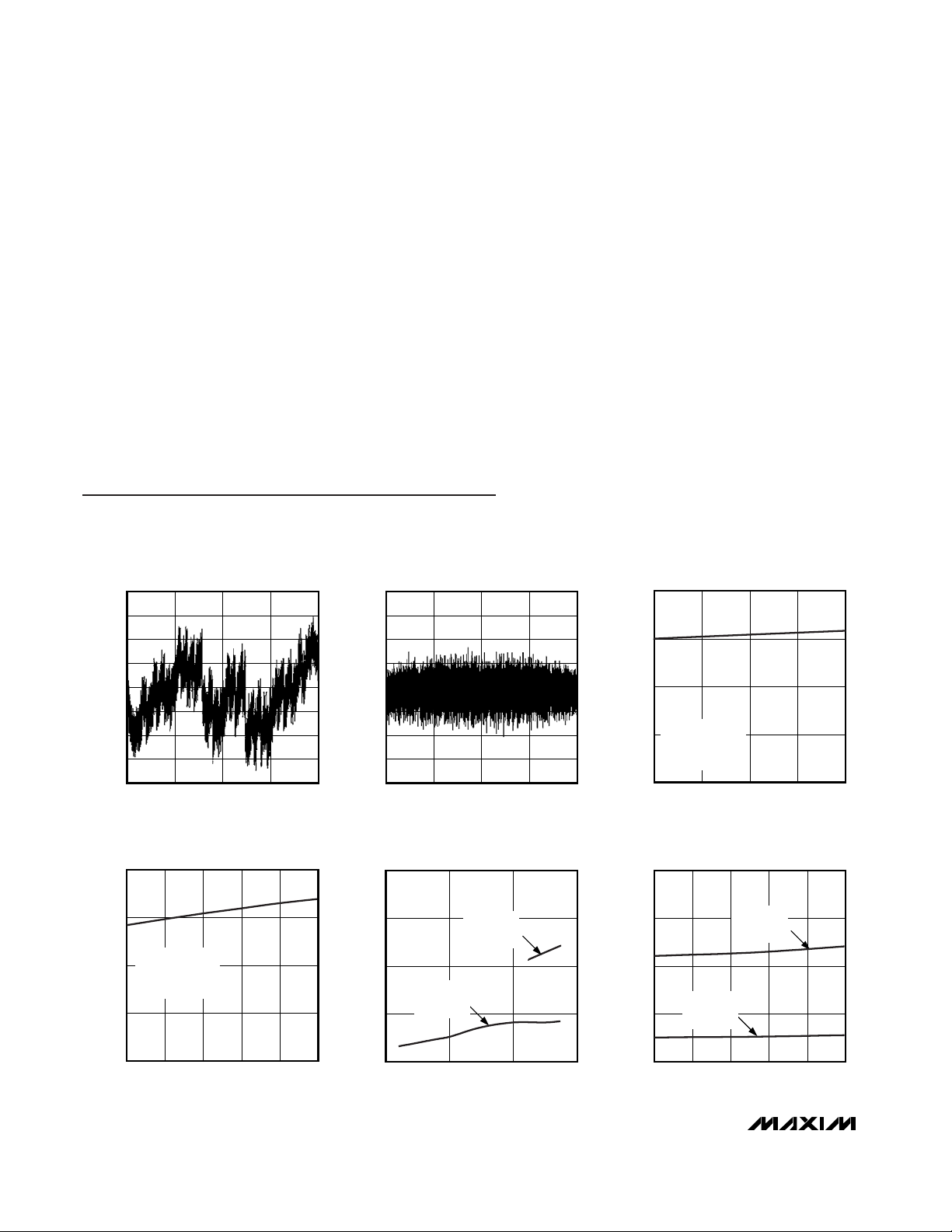
ANALOG SUPPLY CURRENT
vs. SUPPLY VOLTAGE
MAX1316 toc03
SUPPLY VOLTAGE (V)
SUPPLY CURRENT (mA)
5.125.004.87
35
40
45
50
30
4.75 5.25
f
SAMPLE
= 250ksps
ALL 8 CHANNELS
DRIVEN WITH FULLSCALE SINE WAVES
ANALOG SUPPLY CURRENT
vs. TEMPERATURE
MAX1316 toc04
TEMPERATURE (°C)
SUPPLY CURRENT (mA)
603510-15
35
40
45
50
30
-40 85
f
SAMPLE =
250ksps
ALL 8 CHANNELS
DRIVEN WITH FULLSCALE SINE WAVES
SHUTDOWN CURRENT
vs. SUPPLY VOLTAGE
MAX1316 toc05
SUPPLY VOLTAGE (V)
SHUTDOWN CURRENT (µA)
4.53.5
0.2
0.4
0.6
0.8
0
2.5 5.5
ANALOG
SHUTDOWN
CURRENT
DIGITAL
SHUTDOWN
CURRENT
SHUTDOWN CURRENT
vs. TEMPERATURE
MAX1316 toc06
TEMPERATURE (°C)
SHUTDOWN CURRENT (µA)
603510-15
0.2
0.4
0.6
0.8
0
-40 85
ANALOG
SHUTDOWN
CURRENT
DIGITAL
SHUTDOWN
CURRENT
MAX1316–MAX1318/MAX1320–MAX1322/MAX1324–MAX1326
8-/4-/2-Channel, 14-Bit, Simultaneous-Sampling ADCs
with ±10V, ±5V, and 0 to +5V Analog Input Ranges
6 _______________________________________________________________________________________
TIMING CHARACTERISTICS (Figures 3, 4, 5, 6 and 7) (Tables 1, 3) (continued)
Note 7: Shutdown current is measured with analog input floating. The large amplitude of the maximum shutdown current specifi-
cation is due to automatic test equipment limitations.
Note 8: Defined as the change in positive full scale caused by ±5% variation in the nominal supply voltage.
Note 9: CONVST must remain low for at least the acquisition period. The maximum acquisition time is limited by internal capacitor
droop.
Note 10: CS-to-WR and CS-to-RD pins are internally AND together. Setup and hold times do not apply.
Note 11: Minimum clock frequency is limited only by the internal T/H droop rate. Limit the time between the falling edge of CONVST
to the falling edge of EOLC to a maximum of 0.25ms.
Note 12: To avoid T/H droop degrading the sampled analog input signals, the first clock pulse should occur within 10µs of the ris-
ing edge of CONVST, and have a minimum clock frequency of 100kHz.
Typical Operating Characteristics
(AV
DD
= +5V, DVDD= +3V, AGND = DGND = 0V, V
REF
= V
REFMS
= +2.5V (external reference), see the Typical Operating Circuits sec-
tion, f
CLK
= 10MHz, 50% duty cycle, INTCLK/EXTCLK = AGND (external clock), SHDN = DGND, TA = +25°C, unless otherwise noted.)
Page 7
Typical Operating Characteristics (continued)
(AV
DD
= +5V, DVDD= +3V, AGND = DGND = 0V, V
REF
= V
REFMS
= +2.5V (external reference), see the Typical Operating Circuits sec-
tion, f
CLK
= 10MHz, 50% duty cycle, INTCLK/EXTCLK = AGND (external clock), SHDN = DGND, TA = +25°C, unless otherwise noted.)
INTERNAL REFERENCE VOLTAGE
vs. ANALOG SUPPLY VOLTAGE
MAX1316 toc07
AVDD (V)
V
REF
(V)
5.25.14.8 4.9 5.0
2.4997
2.4998
2.4999
2.5000
2.5001
2.5002
2.5003
2.5004
2.4996
4.7 5.3
INTERNAL REFERENCE VOLTAGE
vs. TEMPERATURE
MAX1316 toc08
TEMPERATURE (°C)
V
REF
(V)
6035-15 10
2.497
2.498
2.499
2.500
2.501
2.502
2.503
2.504
2.496
-40 85
OFFSET ERROR vs. SUPPLY VOLTAGE
MAX1316 toc09
AVDD (V)
OFFSET ERROR (LSB)
5.155.054.954.85
-1.5
-1.0
-0.5
0
0.5
1.0
1.5
-2.0
4.75 5.25
NORMALIZED AT TA = +25°C
MAX1316–MAX1318/MAX1320–MAX1322/MAX1324–MAX1326
8-/4-/2-Channel, 14-Bit, Simultaneous-Sampling ADCs
with ±10V, ±5V, and 0 to +5V Analog Input Ranges
_______________________________________________________________________________________ 7
OFFSET ERROR vs. TEMPERATURE
MAX1316 toc10
TEMPERATURE (°C)
OFFSET ERROR (%FSR)
6035-15 10
-0.03
-0.02
-0.01
0
0.02
0.01
0.03
0.04
-0.04
-40 85
NORMALIZED AT TA = +25°C
GAIN ERROR vs. SUPPLY VOLTAGE
MAX1316 toc11
AVDD (V)
GAIN ERROR (LSB)
5.155.054.954.85
10
11
12
13
14
15
16
9
4.75 5.25
GAIN ERROR vs. TEMPERATURE
MAX1316 toc12
TEMPERATURE (°C)
GAIN ERROR (%FSR)
6035-15 10
0.02
0.03
0.04
0.05
0.07
0.06
0.08
0.09
0.01
-40 85
Page 8
Typical Operating Characteristics (continued)
(AV
DD
= +5V, DVDD= +3V, AGND = DGND = 0V, V
REF
= V
REFMS
= +2.5V (external reference), see the Typical Operating Circuits sec-
tion, f
CLK
= 10MHz, 50% duty cycle, INTCLK/EXTCLK = AGND (external clock), SHDN = DGND, TA = +25°C, unless otherwise noted.)
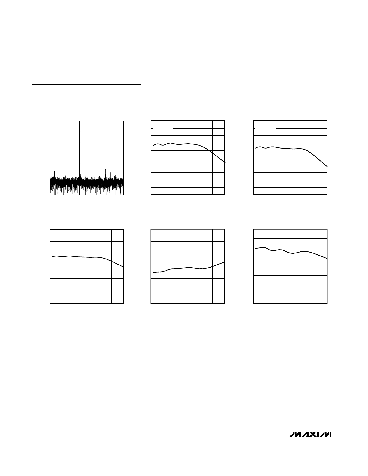
FFT
MAX1316 toc13
FREQUENCY (MHz)
AMPLITUDE (dB)
0.200.150.100.05
-120
-100
-80
-60
-40
-20
0
-140
0 0.25
f
ANALOG_IN
= 103kHz
f
SAMPLE
= 490kHz
f
CLK
= 10MHz
SINAD = 76.7dB
SNR = 77.0dB
THD = -88.3dB
SFDR = 91.0dB
SIGNAL-TO-NOISE RATIO
vs. CLOCK FREQUENCY
MAX1316 toc14
f
CLK
(MHz)
SNR (dB)
1816141210
71
72
73
74
75
76
77
78
79
80
70
820
fIN = 100kHz
SIGNAL-TO-NOISE PLUS DISTORTION
vs. CLOCK FREQUENCY
MAX1316 toc15
f
CLK
(MHz)
SINAD (dB)
1816141210
71
72
73
74
75
76
77
78
79
80
70
820
f
IN
= 100kHz
EFFECTIVE NUMBER OF BITS
vs. CLOCK FREQUENCY
MAX1316 toc16
f
CLK
(MHz)
ENOB (BITS)
1816141210820
11.0
11.5
12.0
12.5
13.0
13.5
10.5
f
IN
= 100kHz
TOTAL HARMONIC DISTORTION
vs. CLOCK FREQUENCY
MAX1316 toc17
f
CLK
(MHz)
THD (dB)
1816141210820
-95
-90
-85
-80
-75
-70
-100
SPURIOUS-FREE DYNAMIC RANGE
vs. CLOCK FREQUENCY
MAX1316 toc17b
f
CLK
(MHz)
SFDR (dB)
1816141210820
65
70
75
80
85
90
95
100
60
MAX1316–MAX1318/MAX1320–MAX1322/MAX1324–MAX1326
8-/4-/2-Channel, 14-Bit, Simultaneous-Sampling ADCs
with ±10V, ±5V, and 0 to +5V Analog Input Ranges
8 _______________________________________________________________________________________
Page 9
OUTPUT HISTOGRAM
(DC INPUT)
MAX1316 toc20
DIGITAL OUTPUT CODE
COUNTS
821782168214 82158211 8212 82138210
500
1000
1500
2000
2500
3000
3500
4000
4500
0
01013
8209
2306
1562
154
341
3815
CONVERSION TIME
vs. TEMPERATURE
MAX1316 toc19
TEMPERATURE (°C)
CONVERSION TIME (µs)
603510-15
0.2
0.4
0.6
0.8
1.0
1.2
1.4
1.6
1.8
2.0
0
-40 85
t
NEXT
t
CONV
INTERNAL CLOCK
CONVERSION TIME
vs. ANALOG SUPPLY VOLTAGE
MAX1316 toc18
ANALOG SUPPLY VOLTAGE (V)
CONVERSION TIME (µs)
5.1255.0004.875
0.2
0.4
0.6
0.8
1.0
1.2
1.4
1.6
1.8
2.0
0
4.750 5.250
t
NEXT
t
CONV
INTERNAL CLOCK
Typical Operating Characteristics (continued)
(AV
DD
= +5V, DVDD= +3V, AGND = DGND = 0V, V
REF
= V
REFMS
= +2.5V (external reference), see the Typical Operating Circuits sec-
tion, f
CLK
= 10MHz, 50% duty cycle, INTCLK/EXTCLK = AGND (external clock), SHDN = DGND, TA = +25°C, unless otherwise noted.)
MAX1316–MAX1318/MAX1320–MAX1322/MAX1324–MAX1326
8-/4-/2-Channel, 14-Bit, Simultaneous-Sampling ADCs
with ±10V, ±5V, and 0 to +5V Analog Input Ranges
_______________________________________________________________________________________ 9
Pin Description
PIN
MAX1316
MAX1320
MAX1324
MAX1317
MAX1321
MAX1325
MAX1318
MAX1322
MAX1326
NAME FUNCTION
1, 15, 17 1, 15, 17 1, 15, 17 AV
DD
Analog Supply Input. AVDD is the power input for the analog section
of the converter. Apply 4.75V to 5.25V to AV
DD
. Bypass AVDD to
AGND (pin 14 to pin 15, pin 16 to pin 17, pin 1 to pin 2) with a 0.1µF
capacitor at each AV
DD
input.
2, 3, 14, 16, 23
AGND
Analog Ground. AGND is the power return for AV
DD
. Connect all
AGNDs together.
4 4 4 CH0 Channel 0 Analog Input
5 5 5 CH1 Channel 1 Analog Input
666MSV
Midscale Voltage Bypass. For the MAX1316/MAX1317/MAX1318,
connect a 2.2µF and a 0.1µF capacitor from MSV to AGND. For the
MAX1320/MAX1321/MAX1322/MAX1324/MAX1325/MAX1326,
connect MSV directly to AGND.
7 7 — CH2 Channel 2 Analog Input
8 8 — CH3 Channel 3 Analog Input
9 — — CH4 Channel 4 Analog Input
2, 3, 14, 16, 23 2, 3, 14, 16, 23
Page 10

MAX1316–MAX1318/MAX1320–MAX1322/MAX1324–MAX1326
8-/4-/2-Channel, 14-Bit, Simultaneous-Sampling ADCs
with ±10V, ±5V, and 0 to +5V Analog Input Ranges
10 ______________________________________________________________________________________
Pin Description (continued)
PIN
MAX1316
MAX1320
MAX1324
MAX1317
MAX1321
MAX1325
MAX1318
MAX1322
MAX1326
NAME FUNCTION
10 — — CH5 Channel 5 Analog Input
11 — — CH6 Channel 6 Analog Input
12 — — CH7 Channel 7 Analog Input
13 13 13
Clock-Mode Select Input. Use INTCLK/EXTCLK to select the internal
or external conversion clock. Connect INTCLK/EXTCLK to AV
DD
to
select the internal clock. Connect INTCLK/EXTCLK to AGND to use
an external clock connected to CLK.
18 18 18 REF
MS
Midscale Reference Bypass or Input. REFMS is the bypass point for
an internally generated reference voltage. For the MAX1316/
MAX1317/MAX1318, connect a 0.1µF capacitor from REF
MS
to
AGND. For the MAX1320/MAX1321/MAX1322/MAX1324/
MAX1325/MAX1326, connect REF
MS
directly to REF and bypass
with a 0.1µF capacitor from REF
MS
to AGND.
19 19 19 REF
ADC Reference Bypass or Input. REF is the bypass point for an
internally generated reference voltage. Bypass REF with a 0.01µF
capacitor to AGND. REF can be driven externally by a precision
external voltage reference.
20 20 20 REF+
Positive Reference Bypass. REF+ is the bypass point for an
internally generated reference voltage. Bypass REF+ with a 0.1µF
capacitor to AGND. Also bypass REF+ to REF- with a 2.2µF and a
0.1µF capacitor.
21 21 21 COM
Reference Common Bypass. COM is the bypass point for an
internally generated reference voltage. Bypass COM to AGND with
a 2.2µF and a 0.1µF capacitor.
22 22 22 REF-
Negative Reference Bypass. REF- is the bypass point for an
internally generated reference voltage. Bypass REF- with a 0.1µF
capacitor to AGND. Also bypass REF- to REF+ with a 2.2µF and a
0.1µF capacitor.
24 24 24 D0
Digital I/O Bit 0 of 14-Bit Parallel Data Bus. High impedance when
RD = 1 or CS = 1.
25 25 25 D1
Digital I/O Bit 1 of 14-Bit Parallel Data Bus. High impedance when
RD = 1 or CS = 1.
26 26 26 D2
Digital I/O Bit 2 of 14-Bit Parallel Data Bus. High impedance when
RD = 1 or CS = 1.
INTCLK/
EXTCLK
Page 11

MAX1316–MAX1318/MAX1320–MAX1322/MAX1324–MAX1326
8-/4-/2-Channel, 14-Bit, Simultaneous-Sampling ADCs
with ±10V, ±5V, and 0 to +5V Analog Input Ranges
______________________________________________________________________________________ 11
Pin Description (continued)
PIN
MAX1316
MAX1320
MAX1324
MAX1317
MAX1321
MAX1325
MAX1318
MAX1322
MAX1326
NAME FUNCTION
27 27 27 D3
Digital I/O Bit 3 of 14-Bit Parallel Data Bus. High impedance when
RD = 1 or CS = 1.
28 28 28 D4
Digital I/O Bit 4 of 14-Bit Parallel Data Bus. High impedance when
RD = 1 or CS = 1.
29 29 29 D5
Digital I/O Bit 5 of 14-Bit Parallel Data Bus. High impedance when
RD = 1 or CS = 1.
30 30 30 D6
Digital I/O Bit 6 of 14-Bit Parallel Data Bus. High impedance when
RD = 1 or CS = 1.
31 31 31 D7
Digital I/O Bit 7 of 14-Bit Parallel Data Bus. High impedance when
RD = 1 or CS = 1.
32 32 32 D8
Digital Out Bit 8 of 14-Bit Parallel Data Bus. High impedance when
RD = 1 or CS = 1.
33 33 33 D9
Digital Out Bit 9 of 14-Bit Parallel Data Bus. High impedance when
RD = 1 or CS = 1.
34 34 34 D10
Digital Out Bit 10 of 14-Bit Parallel Data Bus. High impedance when
RD = 1 or CS = 1.
35 35 35 D11
Digital Out Bit 11 of 14-Bit Parallel Data Bus. High impedance when
RD = 1 or CS = 1.
36 36 36 D12
Digital Out Bit 12 of 14-Bit Parallel Data Bus. High impedance when
RD = 1 or CS = 1.
37 37 37 D13
Digital Out Bit 13 of 14-Bit Parallel Data Bus. High impedance when
RD = 1 or CS = 1.
38 38 38 DV
DD
Digital-Supply Input. Apply +2.7V to +5.25V to DVDD. Bypass DV
DD
to DGND with a 0.1µF capacitor.
39 39 39 DGND
Digital-Supply GND. DGND is the power return for DV
DD
. Connect
DGND to AGND at only one point (see the Layout, Grounding, and
Bypassing section).
40 40 40 EOC
End-of-Conversion Output. EOC goes low to indicate the end of a
conversion. EOC returns high after one clock period.
Page 12

MAX1316–MAX1318/MAX1320–MAX1322/MAX1324–MAX1326
8-/4-/2-Channel, 14-Bit, Simultaneous-Sampling ADCs
with ±10V, ±5V, and 0 to +5V Analog Input Ranges
12 ______________________________________________________________________________________
Pin Description (continued)
PIN
MAX1316
MAX1320
MAX1324
MAX1317
MAX1321
MAX1325
MAX1318
MAX1322
MAX1326
NAME FUNCTION
41 41 41 EOLC
End-of-Last-Conversion Output. EOLC goes low to indicate the end
of the last conversion. EOLC returns high when CONVST goes low
for the next conversion sequence.
42 42 42 RD
Read Input. When RD and CS go low, the device initiates a read
command of the parallel data buses, D0–D13. D0–D13 are high
impedance while either RD or CS is high.
43 43 43 WR
Write Input. The write command initiates when WR and CS go low. A
write command loads the configuration byte on D0–D7.
44 44 44 CS
Chip-Select Input. Pulling CS low activates the digital interface.
D0–D13 are high impedance while either CS or RD is high.
45 45 45
Convert-Start Input. Driving CONVST high places the device in hold
mode and initiates the conversion process. The analog inputs are
sampled on the rising edge of CONVST. When CONVST is low, the
analog inputs are tracked.
46 46 46 CLK
External-Clock Input. CLK accepts an external-clock signal up to
15MHz. Connect CLK to DGND for internally clocked conversions.
To select external-clock mode, set INTCLK/EXTCLK = 0.
47 47 47 SHDN
Shutdown Input. Set SHDN = 0 for normal operation. Set SHDN = 1
for shutdown mode.
48 48 48 ALLON
Enable-All-Channels Input. Drive ALLON high to enable all input
channels. When ALLON is low, only input channels selected as
active are powered. Select channels as active using the
configuration register.
— 9–12 7–12 I.C. Internally Connected. Connect I.C. to AGND. For factory use only.
CONVST
Page 13

MAX1316–MAX1318/MAX1320–MAX1322/MAX1324–MAX1326
8-/4-/2-Channel, 14-Bit, Simultaneous-Sampling ADCs
with ±10V, ±5V, and 0 to +5V Analog Input Ranges
______________________________________________________________________________________ 13
Detailed Description
The MAX1316–MAX1318/MAX1320–MAX1322/MAX1324MAX1326 are 14-bit ADCs. They offer two, four, or eight
(independently selectable) input channels, each with its
own T/H circuitry. Simultaneous sampling of all active
channels preserves relative phase information, making
these devices ideal for motor control and power monitoring. These devices are available with 0 to +5V, ±5V, and
±10V input ranges. The 0 to +5V devices feature ±6V
fault-tolerant inputs. The ±5V and ±10V devices feature
±16.5V fault-tolerant inputs. Two channels convert in 2µs;
all eight channels convert in 3.8µs, with a maximum 8channel throughput of 263ksps per channel. Internal or
external reference and internal- or external-clock capability offer great flexibility and ease of use. A write-only configuration register can mask out unused channels, and a
shutdown feature reduces power. A 16.6MHz, 14-bit, parallel data bus outputs the conversion result. Figure 1
shows the functional diagram of these devices.
Analog Inputs
T/H
To preserve phase information across these multichannel devices, each input channel has a dedicated
T/H amplifier.
Use a low-input source impedance to minimize gainerror harmonic distortion. The time required for the T/H
to acquire an input signal depends on the input source
impedance. If the input signal’s source impedance is
high, the acquisition time lengthens and more time
must be allowed between conversions. The acquisition
time (t
1
) is the maximum time the device takes to
acquire the signal. Use the following formula to calculate acquisition time:
t
1
= 10 (RS+ RIN) x 6pF
where RIN= 2.2kΩ, RS= the input signal’s source
impedance, and t1is never less than 180ns. A source
impedance of less than 100Ω does not significantly
affect the ADC’s performance.
Figure 1. Functional Diagram
MAX1316–MAX1318
MAX1320–MAX1322
MAX1324–MAX1326
CONVST
D13
MSV
DGND
AV
DD
SHDN
CLK
CH0
INTERFACE
AND
CONTROL
8 x 1
MUX
14-BIT
ADC
CH7
D0
DV
DD
AGND
ALLON
REF
MS
REF
REF+
COM
REF-
S/H
S/H
8 x 14
SRAM
OUTPUT
DRIVERS
5kΩ
5kΩ
CONFIGURATION
REGISTER
D7
D8
2.500V
*
*SWITCH CLOSED ON UNIPOLAR DEVICES, OPEN ON BIPOLAR DEVICES
INTCLK/EXTCLK
WR
CS
RD
EOC
EOLC
Page 14

MAX1316–MAX1318/MAX1320–MAX1322/MAX1324–MAX1326
8-/4-/2-Channel, 14-Bit, Simultaneous-Sampling ADCs
with ±10V, ±5V, and 0 to +5V Analog Input Ranges
14 ______________________________________________________________________________________
To improve the input-signal bandwidth under AC conditions, drive the input with a wideband buffer (>50MHz)
that can drive the ADC’s input capacitance and settle
quickly. For example, the MAX4265 can be used for +5V
unipolar devices, or the MAX4350 can be used for ±5V
bipolar inputs.
The T/H aperture delay is typically 13ns. The aperturedelay mismatch between T/Hs of 50ps allows the relative
phase information of up to eight different inputs to be
preserved. Figure 2 shows a simplified equivalent input
circuit, illustrating the ADC’s sampling architecture.
Input Bandwidth
The input tracking circuitry has a 12MHz small-signal
bandwidth, making it is possible to digitize high-speed
transient events and measure periodic signals with
bandwidths exceeding the ADC’s sampling rate by using
undersampling techniques. To avoid high-frequency
signals being aliased into the frequency band of interest,
anti-alias filtering is recommended.
Input Range and Protection
These devices provide ±10V, ±5V, or 0 to +5V analog
input voltage ranges. Figure 2 shows the equivalent input
circuit. Overvoltage protection circuitry at the analog
input provides ±16.5V fault protection for the bipolar input
devices and ±6.0V fault protection for the unipolar input
devices. This fault-protection circuit limits the current
going into or out of the device to less than 50mA, providing an added layer of protection from momentary overvoltage or undervoltage conditions at the analog input.
Power-Saving Modes
Shutdown Mode
During shutdown, the analog and digital circuits in the
device power down and the device draws less than
100µA from AVDD, and less than 100µA from DVDD.
Select shutdown mode using the SHDN input. Set SHDN
high to enter shutdown mode. After coming out of shutdown, allow a 1ms wake-up time before making the first
conversion. When using an external clock, apply at least
20 clock cycles with CONVST high before making the first
conversion. When using internal-clock mode, wait at least
2µs before making the first conversion.
ALLON
ALLON is useful when some of the analog input channels
are selected (see the Configuration Register section).
Drive ALLON high to power up all input channel circuits,
regardless of whether they are selected as active by the
configuration register. Drive ALLON low or connect to
ground to power only the input channels selected as
active by the configuration register, saving 2mA per
channel (typ). The wake-up time for any channel turned
on with the configuration register is 2µs (typ) when
ALLON is low. The wake-up time with ALLON high is
only 0.01µs. New configuration-register information
does not become active until the next CONVST falling
edge. Therefore, when using software to control power
states (ALLON = 0), pulse CONVST low once before
applying the actual CONVST signal (Figure 3). With an
external clock, apply at least 15 clock cycles before
the second CONVST. If using internal-clock mode, wait
at least 1.5µs or until the first EOC before generating
the second CONVST.
Figure 2. Typical Input Circuit
CH_
R1
R2
V
BIAS
C
PAR
1pF
5pF
MAX1316–MAX1318
MAX1320–MAX1322
MAX1324–MAX1326
INPUT RANGE (V)
0 TO +5
±5
±10
R1 (kΩ)
3.33
6.67
13.33
R2 (kΩ)
5.00
2.86
2.35
V
BIAS
(V)
0.90
2.50
2.06
Table 1. Conversion Times Using the
Internal Clock
NUMBER OF CHANNELS
INTERNAL-CLOCK
CONVERSION TIME
1 1.6
2 1.9
3 2.2
4 2.5
5 2.8
6 3.1
7 3.4
8 3.7
Page 15

MAX1316–MAX1318/MAX1320–MAX1322/MAX1324–MAX1326
8-/4-/2-Channel, 14-Bit, Simultaneous-Sampling ADCs
with ±10V, ±5V, and 0 to +5V Analog Input Ranges
______________________________________________________________________________________ 15
Clock Modes
These devices provide an internal clock of 10MHz
(typ). Alternatively, an external clock can be used.
Internal Clock
Internal-clock mode frees the microprocessor from the
burden of running the ADC conversion clock. For internalclock operation, connect INTCLK/EXTCLK to AVDDand
connect CLK to DGND. Table 1 illustrates the total conversion time using internal-clock mode.
External Clock
For external-clock operation, connect INTCLK/EXTCLK
to AGND and connect an external-clock source to CLK.
Note that INTCLK/EXTCLK is referenced to the analog
power supply, AVDD. The external-clock frequency can
be up to 15MHz, with a duty cycle between 30% and
70%. Clock frequencies of 100kHz and lower can be
used, but the droop in the T/H circuits reduce linearity.
Selecting an Input Buffer
Most applications require an input buffer to achieve 14bit accuracy. Although slew-rate and bandwidth are
important, the most critical specification is settling time.
The sampling requires a relatively brief sampling interval of 150ns. At the beginning of the acquisition, the
internal sampling capacitor array connects to CH_ (the
amplifier output), causing some output disturbance.
Ensure the amplifier is capable of settling to at least 14bit accuracy during this interval. Use a low-noise, lowdistortion, wideband amplifier (such as the MAX4350 or
MAX4265), which settles quickly and is stable with the
ADC’s capacitive load (in parallel with any bypass
capacitors on the analog inputs).
Applications Section
Digital Interface
The bidirectional, parallel, digital interface sets the 8-bit
configuration register (see the Configuration Register
section) and outputs the 14-bit conversion result. The
interface includes the following control signals: chip
select (CS), read (RD), write (WR), end of conversion
(EOC), end of last conversion (EOLC), convert start
(CONVST), shutdown (SHDN), all on (ALLON), internalclock select (INTCLK /EXTCLK), and external-clock input
(CLK). Figures 4, 5, 6, 7, Table 4, and the Timing
Characteristics section show the operation of the interface. D0–D7 are bidirectional, and D8–D13 are output
only. All bits are high impedance when RD = 1 or CS = 1.
Configuration Register
Enable channels as active by writing to the configuration
register through I/O lines D0–D7 (Table 2). The bits in the
configuration register map directly to the channels, with
D0 controlling channel zero, and D7 controlling channel
seven. Setting any bit high activates the corresponding
input channel, while resetting any bit low deactivates the
corresponding channel. Devices with fewer than eight
channels contain some bits that have no function.
Figure 3. Software Channel Wake-Up Timing (ALLON = 0)
CONVST
D0–D7
CLK
WR
EOC
EOLC
LATCH
t
ACQ
t
ACQ
DUMMY
CONVERSION
START
ACTUAL
CONVERSION
START
DATA-IN
DATA-IN CHANGES ONE OR MORE CHANNELS
FROM POWER-DOWN TO ACTIVE MODE
12345 1415 1
>14 CYCLES
SAMPLE
Page 16

MAX1316–MAX1318/MAX1320–MAX1322/MAX1324–MAX1326
8-/4-/2-Channel, 14-Bit, Simultaneous-Sampling ADCs
with ±10V, ±5V, and 0 to +5V Analog Input Ranges
16 ______________________________________________________________________________________
To write to the configuration register, pull CS and WR
low, load bits D0–D7 onto the parallel bus, and force
WR high. The data are latched on the rising edge of
WR (Figure 4). It is possible to write to the configuration
register at any point during the conversion sequence;
however, it is not active until the next convert-start signal. At power-up, write to the configuration register to
select the active channels before beginning a conversion. Shutdown does not change the configuration register. See the Shutdown Mode and the ALLON sections
for information about using the configuration register for
power saving.
Starting a Conversion
To start a conversion using internal-clock mode, pull
CONVST low for at least the acquisition time (t1). The
T/H acquires the signal while CONVST is low, and conversion begins on the rising edge of CONVST. An endof-conversion signal (EOC) pulses low when the first
result becomes available, and for each subsequent
result until the end of the conversion cycle. The end-oflast-conversion signal (EOLC) goes low when the last
conversion result is available (Figures 5, 6, and 7).
To start a conversion using external-clock mode, pull
CONVST low for at least the acquisition time (t1). The T/H
acquires the signal while CONVST is low, and conversion
begins on the rising edge of CONVST. Apply an external
clock to CLK. To avoid T/H droop degrading the sampled
analog input signals, the first clock pulse should occur
within 10µs from the rising edge of CONVST, and have a
minimum clock frequency of 100kHz. The first conversion
result is available for read on the rising edge of the 17th
clock cycle, and subsequent conversions after every third
clock cycle thereafter (Figures 5, 6, and 7).
In both internal- and external-clock modes, CONVST
must be held high until the last conversion result is
read. For best operation, the rising edge of CONVST
must be a clean, high-speed, low-jitter digital signal.
Table 3 shows the total throughput as a function of the
clock frequency and the number of channels selected
for conversion. The calculations use the nominal speed
of the internal clock (10MHz) and a 200ns CONVST
pulse width.
Table 2. Configuration Register
BIT/CHANNEL
PART NO.
STATE
D7/CH7
ON11111111
MAX1316
MAX1320
MAX1324
OFF00000000
ON1111NANANANA
MAX1317
MAX1321
MAX1325
OFF0000NANANANA
ON 1 1 NA NA NA NA NA NA
MAX1318
MAX1322
MAX1326
OFF 0 0 NA NA NA NA NA NA
NA = Not applicable.
Figure 4. Write Timing
D0–D7
DATA-IN
RD
CS
WR
t
2
t
5
t
6
t
14
t
15
t
7
D0/CH0 D1/CH1 D2/CH2 D3/CH3 D4/CH4 D5/CH5 D6/CH6
Page 17

MAX1316–MAX1318/MAX1320–MAX1322/MAX1324–MAX1326
8-/4-/2-Channel, 14-Bit, Simultaneous-Sampling ADCs
with ±10V, ±5V, and 0 to +5V Analog Input Ranges
______________________________________________________________________________________ 17
Data Throughput
The data throughput (fTH) of the MAX1316–MAX1318/
MAX1320–MAX1322/MAX1324–MAX1326 is a function
of the clock speed (f
CLK
). In internal-clock mode, f
CLK
=
10MHz. In external-clock mode, 100kHz ≤ f
CLK
≤
12.5MHz. When reading during conversion (Figures 5
and 6), calculate fTHas follows:
where N is the number of active channels and t
QUIET
includes acquistion time t
ACQ
. t
QUIET
is the period of bus
inactivity before the rising edge of CONVST. Typically use
t
QUIET
= t
ACQ
+ 50ns, and prevent disturbance on the
output bus from corrupting signal acquistion. See the
Starting a Conversion section for more information.
Reading a Conversion Result
Reading During a Conversion
Figures 5 and 6 show the interface signals for initiating a
read operation during a conversion cycle. These figures
show two channels selected for conversion. If more channels are selected, the results are available successively
every third clock cycle. CS can be low at all times; it can
be low during the RD cycles, or it can be the same as RD.
After initiating a conversion by bringing CONVST high,
wait for EOC to go low (about 1.6 µs in internal-clock
mode or 17 clock cycles in external-clock mode) before
reading the first conversion result. Read the conversion
result by bringing RD low, thus latching the data to the
parallel digital-output bus. Bring RD high to release the
digital bus. Wait for the next falling edge of EOC (about
300ns in internal-clock mode or three clock cycles in
external-clock mode) before reading the next result.
When the last result is available, EOLC goes low.
f
t
xN
f
TH
QUIET
CLK
=
+
+−+
1
16 3 1 1()
Table 3. Throughput vs. Channels Sampled (t
QUIET
= t
ACQ
= 200ns, f
CLK
= 10MHz)
CHANNELS
SAMPLED
(N)
CLOCK CYCLES
UNTIL LAST
RESULT
CLOCK CYCLE FOR
READING LAST
CONVERSION
TOTAL
CONVERSION
TIME (ns)
SAMPLES PER
SECOND
(ksps)
THROUGHPUT
PER CHANNEL
(ksps)
1 16 1 1900 526 526
2 19 1 2200 909 455
3 22 1 2500 1200 400
4 25 1 2800 1429 357
5 28 1 3100 1613 323
6 31 1 3400 1765 294
7 34 1 3700 1892 270
8 37 1 4000 2000 250
Figure 5. Read During Conversion—Two Channels Selected, Internal Clock
CONVST
CH0
TRACK
HOLD
D0–D13
SAMPLE
t
1
t
13
t
12
t
10
t
3
t
11
TRACK
CH1
t
CONV
t
NEXT
EOC
RD
t
20
Page 18

MAX1316–MAX1318/MAX1320–MAX1322/MAX1324–MAX1326
8-/4-/2-Channel, 14-Bit, Simultaneous-Sampling ADCs
with ±10V, ±5V, and 0 to +5V Analog Input Ranges
18 ______________________________________________________________________________________
Figure 6. Read During Conversion—Two Channels Selected, External Clock
CONVST
CLK
CH0
TRACK
HOLD
D0–D13
SAMPLE
t
ACQ
t
19
t
13
t
12
t
QUIET
t
10
t
3
t
11
TRACK
CH1
EOC
RD
1 2 3 16 17 18 19 20 21 22 23 1
t
16
t
17
t
18
Figure 7. Reading After Conversion—Eight Channels Selected, External Clock
CLK
D0–D13
CONVST
TRACK
HOLD
SAMPLE
t
ACQ
t
19
t
13
1 2 38 39 40 41 42 43
t
17
t
8
t
10
t
11
t
3
t
4
t
9
t
18
t
16
t
12
t
QUIET
CH0 CH1 CH2 CH3 CH4 CH5 CH6 CH7
ONLY LAST PULSE SHOWN
EOC
RD
CS
EOLC
Page 19

MAX1316–MAX1318/MAX1320–MAX1322/MAX1324–MAX1326
8-/4-/2-Channel, 14-Bit, Simultaneous-Sampling ADCs
with ±10V, ±5V, and 0 to +5V Analog Input Ranges
______________________________________________________________________________________ 19
Reading After Conversion
Figure 7 shows the interface signals for a read operation
after a conversion with all eight channels enabled. At the
falling edge of EOLC, on the 38th clock pulse after the initiation of a conversion, driving CS and RD low places the
first conversion result onto the parallel bus, which can be
latched on the rising edge of RD. Successive low pulses
of RD place the successive conversion results onto the
bus. Pulse CONVST low to initiate a new conversion.
Power-Up Reset
At power-up, all channels are selected for conversion
(see the Configuration Register section). After applying
power, allow a 1.0ms wake-up time to elapse before initiating the first conversion. Then, hold CONVST high for
at least 2.0µs after the wake-up time is complete. If
using an external clock, apply 20 clock pulses to CLK
with CONVST high before initiating the first conversion.
Reference
Internal Reference
The internal-reference circuits provide for analog input
voltages of 0 to +5V unipolar (MAX1316/MAX1317/
MAX1318), ±5V bipolar (MAX1320/MAX1321/MAX1322),
or ±10V bipolar (MAX1324/MAX1325/MAX1326). Install
external capacitors for reference stability, as indicated in
Table 4, and as shown in the Typical Operating Circuits.
External Reference
Connect a +2.0V to +3.0V external reference at REF
MS
and/or REF. When connecting an external reference, the
input impedance is typically 5kΩ. The external reference
must be able to drive 200µA of current and have a low
output impedance. For more information about using
external references see the Transfer Functions section.
Layout, Grounding, and Bypassing
For best performance use PC boards with ground
planes. Board layout should ensure that digital and
analog signal lines are separated from each other. Do
not run analog and digital lines parallel to one another
(especially clock lines), or do not run digital lines
underneath the ADC package. Figure 8 shows the recommended system ground connections when not using
a ground plane. A single-point analog ground (star
ground point) should be established at AGND, separate from the logic ground. All other analog grounds
and DGND should be connected to this ground.
Figure 8. Power-Supply Grounding and Bypassing
Table 4. Reference Bypass Capacitors
INPUT VOLTAGE RANGE
LOCATION
UNIPOLAR (µF) BIPOLAR (µF)
MSV bypass capacitor to AGND 2.2 || 0.1 NA
REFMS bypass capacitor to AGND 0.01 0.01 (connect REFMS to REF)
REF bypass capacitor to AGND 0.01 0.01 (connect REFMS to REF)
REF+ bypass capacitor to AGND 0.1 0.1
REF+ to REF- capacitor 2.2 || 0.1 2.2 || 0.1
REF- bypass capacitor to AGND 0.1 0.1
COM bypass capacitor to AGND 2.2 || 0.1 2.2 || 0.1
NA = Not applicable (connect MSV directly to AGND).
SUPPLIES
AV
DD AGND DGND
V
DD
DIGITAL
CIRCUITRY
OPTIONAL
FERRITE
BEAD
+5V RETURN RETURN+3V TO +5V
DV
DD
GND
MAX1316–MAX1318
MAX1320–MAX1322
MAX1324–MAX1326
Page 20

MAX1316–MAX1318/MAX1320–MAX1322/MAX1324–MAX1326
8-/4-/2-Channel, 14-Bit, Simultaneous-Sampling ADCs
with ±10V, ±5V, and 0 to +5V Analog Input Ranges
20 ______________________________________________________________________________________
No other digital system ground should be connected to
this single-point analog ground. The ground return to
the power supply for this ground should be low impedance and as short as possible for noise-free operation.
High-frequency noise in the VDDpower supply may
affect the high-speed comparator in the ADC. Bypass
these supplies to the single-point analog ground with
0.1µF and 2.2µF bypass capacitors close to the device.
If the +5V power supply is very noisy, a ferrite bead can
be connected as a lowpass filter, as shown in Figure 8.
Transfer Functions
Bipolar ±10V Devices
Table 5 and Figure 9 show the two’s complement transfer function for the MAX1324/MAX1325/MAX1326 with a
±10V input range. The full-scale input range (FSR) is
eight times the voltage at REF. The internal +2.500V reference gives a +20V FSR, while an external +2V to +3V
reference allows an FSR of +16V to +24V, respectively.
Calculate the LSB size using the following equation:
This equals 1.2207mV with a +2.5V internal reference.
The input range is centered about V
MSV
. Normally,
MSV = AGND, and the input is symmetrical about zero.
For a custom midscale voltage, drive MSV with an
external voltage source. Noise present on MSV directly
couples into the ADC result. Use a precision, low-drift
voltage reference with adequate bypassing to prevent
MSV from degrading ADC performance. For maximum
FSR, be careful not to violate the absolute maximum
voltage ratings of the analog inputs when choosing
V
MSV
.
Determine the input voltage as a function of V
REF
,
V
MSV
, and the output code in decimal using the follow-
ing equation:
Bipolar ±5V Devices
Table 6 and Figure 10 show the two’s complement
transfer function for the MAX1320/MAX1321/MAX1322
with a ±5V input range. The FSR is four times the voltage at REF. The internal +2.500V reference gives a
+10V FSR, while an external +2V to +3V reference
allows an FSR of +8V to +12V, respectively. Calculate
the LSB size using the following equation:
This equals 0.6104mV when using the internal reference.
LSB
V
REF
=×4
2
14
V LSB CODE V
CH MSV_
=× +
10
LSB
V
REF
=×8
2
14
Figure 9. ±10V Bipolar Transfer Function
8 x V
REF
8 x V
REF
8 x V
REF
2
14
1 LSB =
TWO'S COMPLEMENT BINARY OUTPUT CODE
-8192 -8190 +8191+8189
0x2000
0x2001
0x2002
0x2003
0x1FFF
0x1FFE
0x1FFD
0x1FFC
0x3FFF
0x0000
0x0001
-1 0 +1
(MSV)
INPUT VOLTAGE (V
CH_
- V
MSV
IN LSBs)
Table 5. ±10V Bipolar Code Table
TWO’S COMPLEMENT
BINARY OUTPUT CODE
DECIMAL
OUTPUT
(CODE
10
)
INPUT
VOLTAGE (V)
(V
REF
= 2.5V,
V
MSV
= 0V)
01 1111 1111 1111
0x1FFF
8191
9.9994
±0.5 LSB
01 1111 1111 1110
0x1FFE
8190
9.9982
±0.5 LSB
00 0000 0000 0001
0x0001
1
0.0018
±0.5 LSB
00 0000 0000 0000
0x0000
0
0.0006
±0.5 LSB
11 1111 1111 1111
0x3FFF
-1
-0.0006
±0.5 LSB
10 0000 0000 0001
0x2001
-8191
-9.9982
±0.5 LSB
10 0000 0000 0000
0x2000
-8192
-9.9994
±0.5 LSB
EQUIVALENT
Page 21

MAX1316–MAX1318/MAX1320–MAX1322/MAX1324–MAX1326
8-/4-/2-Channel, 14-Bit, Simultaneous-Sampling ADCs
with ±10V, ±5V, and 0 to +5V Analog Input Ranges
______________________________________________________________________________________ 21
The input range is centered about V
MSV
. Normally,
MSV = AGND, and the input is symmetrical about zero.
For a custom midscale voltage, drive MSV with an
external voltage source. Noise present on MSV directly
couples into the ADC result. Use a precision, low-drift
voltage reference with adequate bypassing to prevent
MSV from degrading ADC performance. For maximum
FSR, be careful not to violate the absolute maximum
voltage ratings of the analog inputs when choosing
V
MSV
. Determine the input voltage as a function of
V
REF
, V
MSV
, and the output code in decimal using the
following equation:
Unipolar 0 to +5V Devices
Table 7 and Figure 11 show the offset binary transfer
function for the MAX1316/MAX1317/MAX1318 with a 0
to +5V input range. The FSR is two times the voltage at
REF. The internal +2.500V reference gives a +5V FSR,
while an external +2V to +3V reference allows an FSR
of +4V to +6V, respectively. Calculate the LSB size
using the following equation:
This equals 0.3052mV when using the internal reference.
LSB
V
REF
=×2
2
14
V LSB CODE V
CH MSV_
=× +
10
Figure 10. ±5V Bipolar Transfer Function
4 x V
REF
4 x V
REF
4 x V
REF
2
14
1 LSB =
TWO'S COMPLEMENT BINARY OUTPUT CODE
-8192 -8190 +8191+8189
0x2000
0x2001
0x2002
0x2003
0x1FFF
0x1FFE
0x1FFD
0x1FFC
0x3FFF
0x0000
0x0001
-1 0 +1
(MSV)
INPUT VOLTAGE (V
CH_
- V
MSV
IN LSBs)
Table 6. ±5V Bipolar Code Table
TWO’S COMPLEMENT
BINARY OUTPUT CODE
DECIMAL
OUTPUT
(CODE
10
)
INPUT
VOLTAGE (V)
(V
REF
= 2.5V,
V
MSV
= 0V)
01 1111 1111 1111
0x1FFF
8191
4.9997
±0.5 LSB
01 1111 1111 1110
0x1FFE
8190
4.9991
±0.5 LSB
00 0000 0000 0001
0x0001
1
0.0009
±0.5 LSB
00 0000 0000 0000
0x0000
0
0.0003
±0.5 LSB
11 1111 1111 1111
0x3FFF
-1
-0.0003
±0.5 LSB
10 0000 0000 0001
0x2001
-8191
-4.9991
±0.5 LSB
10 0000 0000 0000
0x2000
-8192
-4.9997
±0.5 LSB
Table 7. 0 to +5V Unipolar Code Table
BINARY OUTPUT CODE
DECIMAL
OUTPUT
(CODE
10
)
INPUT
VOLTAGE (V)
(V
REF
= V
REFMS
= 2.5V)
11 1111 1111 1111
0x3FFF
16383
4.9998
±0.5 LSB
11 1111 1111 1110
0x3FFE
16382
4.9995
±0.5 LSB
10 0000 0000 0001
0x2001
8193
2.5005
±0.5 LSB
10 0000 0000 0000
0x2000
8192
2.5002
±0.5 LSB
01 1111 1111 1111
0x1FFF
8191
2.4998
±0.5 LSB
00 0000 0000 0001
0x0001
1
0.0005
±0.5 LSB
00 0000 0000 0000
0x0000
0
0.0002
±0.5 LSB
EQUIVALENT
EQUIVALENT
Page 22

MAX1316–MAX1318/MAX1320–MAX1322/MAX1324–MAX1326
8-/4-/2-Channel, 14-Bit, Simultaneous-Sampling ADCs
with ±10V, ±5V, and 0 to +5V Analog Input Ranges
22 ______________________________________________________________________________________
The input range is centered about V
MSV
, which is internally set to +2.500V. For a custom midscale voltage,
drive REFMSwith an external voltage source and MSV
will follow REFMS. Noise present on MSV or REF
MS
directly couples into the ADC result. Use a precision,
low-drift voltage reference with adequate bypassing to
prevent MSV from degrading ADC performance. For
maximum FSR, be careful not to violate the absolute
maximum voltage ratings of the analog inputs when
choosing V
MSV
. Determine the input voltage as a func-
tion of V
REF
, V
MSV
, and the output code in decimal
using the following equation:
Definitions
Integral Nonlinearity
Integral nonlinearity (INL) is the deviation of the values
on an actual transfer function from a straight line. For
these devices, this straight line is a line drawn between
the end points of the transfer function, once offset and
gain errors have been nullified.
Differential Nonlinearity
Differential nonlinearity (DNL) is the difference between
an actual step width and the ideal value of 1 LSB. For
these devices, the DNL of each digital output code is
measured and the worst-case value is reported in the
Electrical Characteristics table. A DNL error specification of less than ±1 LSB guarantees no missing codes
and a monotonic transfer function.
Unipolar Offset Error
For the unipolar MAX1316/MAX1317/MAX1318, the ideal
zero-scale transition from 0x0000 to 0x0001 occurs at
1 LSB (see Figure 11). The unipolar offset error is the
amount of deviation between the measured zero-scale
transition point and the ideal zero-scale transition point.
Bipolar Offset Error
For the bipolar MAX1320/MAX1321/MAX1322/
MAX1324/MAX1325/MAX1326, the ideal zero-point transition from 0x3FFF to 0x0000 occurs at MSV, which is
usually connected to ground (see Figures 9 and 10).
The bipolar offset error is the amount of deviation
between the measured zero-point transition and the
ideal zero-point transition.
Gain Error
The ideal full-scale transition from 0x1FFE to 0x1FFF
occurs at 1 LSB below full scale (see the Transfer
Functions section). The gain error is the amount of deviation between the measured full-scale transition point
and the ideal full-scale transition point, once offset error
has been nullified.
Signal-to-Noise Ratio
For a waveform perfectly reconstructed from digital
samples, signal-to-noise ratio (SNR) is the ratio of the
full-scale analog input (RMS value) to the RMS quantization error (residual error). The ideal, theoretical minimum analog-to-digital noise is caused by quantization
noise error only and results directly from the ADC’s resolution (N bits):
where N = 14 bits.
In reality, there are other noise sources besides quanti-
zation noise: thermal noise, reference noise, clock jitter,
etc. SNR is computed by taking the ratio of the RMS
signal to the RMS noise, which includes all spectral
components minus the fundamental, the first five harmonics, and the DC offset.
SNR N dB=×+(. . )602 176
V LSB CODE V
CH MSV_
=× +
()
10
- 2.500V
Figure 11. 0 to +5V Unipolar Transfer Function
2 x V
REF
2 x V
REF
2 x V
REF
2
14
1 LSB =
BINARY OUTPUT CODE
0 2 16,38316,381
0x0000
0x0001
0x0002
0x0003
0x3FFF
0x3FFE
0x3FFD
0x3FFC
0x1FFF
0x2000
0x2001
8190
8192
8194
(MSV)
INPUT VOLTAGE (LSBs)
Page 23

MAX1316–MAX1318/MAX1320–MAX1322/MAX1324–MAX1326
8-/4-/2-Channel, 14-Bit, Simultaneous-Sampling ADCs
with ±10V, ±5V, and 0 to +5V Analog Input Ranges
______________________________________________________________________________________ 23
Signal-to-Noise Plus Distortion
Signal-to-noise plus distortion (SINAD) is the ratio of the
fundamental input frequency’s RMS amplitude to the
RMS equivalent of all the other ADC output signals:
Effective Number of Bits
The effective number of bits (ENOB) indicates the global
accuracy of an ADC at a specific input frequency and
sampling rate. An ideal ADC’s error consists of quantization noise only. With an input range equal to the fullscale range of the ADC, calculate the ENOB as follows:
Total Harmonic Distortion
Total harmonic distortion (THD) is the ratio of the RMS
sum of the first five harmonics of the input signal to the
fundamental itself. This is expressed as:
where V1is the fundamental amplitude and V2 through
V5are the 2nd- through 5th-order harmonics.
Spurious-Free Dynamic Range
Spurious-free dynamic range (SFDR) is the ratio of the
RMS amplitude of the fundamental (maximum signal
component) to the RMS value of the next-largest frequency component.
Aperture Delay
Aperture delay (tAD) is the time delay from the sampling
clock edge to the instant when an actual sample is taken.
Aperture Jitter
Aperture Jitter (tAJ) is the sample-to-sample variation in
aperture delay.
Channel-to-Channel Isolation
Channel-to-channel isolation indicates how well each
analog input is isolated from the other channels. Channelto-channel isolation is measured by applying DC to channels 1 to 7, while a -0.5dBFS sine wave is applied to
channel 0. A 100kHz FFT is taken for channel 0 and
channel 1. Channel-to-channel isolation is expressed in
dB as the power ratio of the two 100kHz magnitudes.
Small-Signal Bandwidth
A small -20dBFS analog input signal is applied to an
ADC in a manner that ensures that the signal’s slew
rate does not limit the ADC’s performance. The input
frequency is then swept up to the point where the
amplitude of the digitized conversion result has
decreased 3dB.
Full-Power Bandwidth
A large -0.5dBFS analog input signal is applied to an
ADC, and the input frequency is swept up to the point
where the amplitude of the digitized conversion result
has decreased by 3dB. This point is defined as fullpower input bandwidth frequency.
Chip Information
TRANSISTOR COUNT: 80,000
PROCESS: BiCMOS 0.6µm
THD
VVVV
V
=×
+++
⎡
⎣
⎢
⎢
⎢
⎤
⎦
⎥
⎥
⎥
20
2
2
3
2
4
2
5
2
1
log
ENOB
SINAD=-176
602..
SINAD dB
Signal
Noise Distortion
RMS
RMS
( ) log
()
=×
+
⎡
⎣
⎢
⎤
⎦
⎥
20
Page 24

MAX1316–MAX1318/MAX1320–MAX1322/MAX1324–MAX1326
8-/4-/2-Channel, 14-Bit, Simultaneous-Sampling ADCs
with ±10V, ±5V, and 0 to +5V Analog Input Ranges
24 ______________________________________________________________________________________
Typical Operating Circuits
MAX1316
MAX1317
MAX1318
CH0
CH7
CH6
CH5
CH4
CH3
CH2
CH1
D12
D0
D1
D2
D3
D4
D5
D6
D7
D8
D9
D10
D11
AV
DD
AGND
DV
DD
DGND
MSV
REF
MS
REF
REF+
COM
REF-
+5V
GND
+3V
GND
D13
SHDN
ALLON
ANALOG
INPUTS
0 TO +5V
PARALLEL
DIGITAL
OUTPUT
CONVST
CLK
DIGITAL
INTERFACE
AND
CONTROL
4
5
7
8
9
10
11
12
2, 3, 14, 16, 23
21
22
20
19
18
6
17
44
42
43
38
45
47
48
46
40
41
37
36
35
34
33
32
31
30
29
28
27
26
25
24
39
13
AV
DD
AV
DD
15
1
0.1µF
0.1µF
0.1µF
0.1µF
0.1µF
0.1µF
0.1µF
0.1µF
0.01µF
0.1µF
0.01µF
2.2µF
2.2µF
2.2µF
MAX1316
MAX1317
MAX1318
UNIPOLAR
CONFIGURATION
INTCLK/EXTCLK
CS
RD
WR
EOC
EOLC
PARALLEL
DIGITAL
I/O
Page 25

MAX1316–MAX1318/MAX1320–MAX1322/MAX1324–MAX1326
8-/4-/2-Channel, 14-Bit, Simultaneous-Sampling ADCs
with ±10V, ±5V, and 0 to +5V Analog Input Ranges
______________________________________________________________________________________ 25
Typical Operating Circuits (continued)
MAX1320
MAX1321
MAX1322
MAX1324
MAX1325
MAX1326
CH0
CH7
CH6
CH5
CH4
CH3
CH2
CH1
D12
D0
D1
D2
D3
D4
D5
D6
D7
D8
D9
D10
D11
AV
DD
AGND
DV
DD
DGND
MSV
REF
MS
REF
REF+
COM
REF-
+5V
GND
+3V
GND
D13
SHDN
ALLON
BIPOLAR
ANALOG
INPUTS
CONVST
CLK
DIGITAL
INTERFACE
AND
CONTROL
4
5
7
8
9
10
11
12
2, 3, 14, 16, 23
21
22
20
19
18
6
17
44
42
43
38
45
47
48
46
40
41
37
36
35
34
33
32
31
30
29
28
27
26
25
24
39
13
AV
DD
AV
DD
15
1
0.1µF
0.1µF
0.1µF
0.1µF
0.1µF
0.1µF
0.1µF
0.01µF
0.1µF
2.2µF
2.2µF
MAX1322
MAX1324
MAX1320
MAX1325
MAX1321
MAX1326
BIPOLAR
CONFIGURATION
INTCLK/EXTCLK
CS
RD
WR
EOC
EOLC
PARALLEL
DIGITAL
OUTPUT
PARALLEL
DIGITAL
I/O
Page 26

MAX1316–MAX1318/MAX1320–MAX1322/MAX1324–MAX1326
8-/4-/2-Channel, 14-Bit, Simultaneous-Sampling ADCs
with ±10V, ±5V, and 0 to +5V Analog Input Ranges
26 ______________________________________________________________________________________
Pin Configurations
D12
D11
D10
D9
D8
D7
D6
D5
D4
D3
D2
D1
AVDD
AGND
AGND
CH0
CH1
MSV
CH2
CH3
CH4
CH5
CH6
CH7
1
2
3
4
5
6
7
8
9
10
11
12
36
35
34
33
32
31
30
29
28
27
26
25
8-CHANNEL TQFP
MAX1316
MAX1320
MAX1324
INTCLK/EXTCLK
AGND
AV
DD
AGND
AVDD
REFMS
REF
REF+
COM
REF-
AGND
D0
1314151617181920212223
24
4847464544434241403938
37
ALLON
SHDN
CLK
CONVSTCSWRRDEOLC
EOC
DGND
DVDD
D13
D12
D11
D10
D9
D8
D7
D6
D5
D4
D3
D2
D1
AVDD
AGND
AGND
CH0
CH1
MSV
CH2
CH3
I.C.
I.C.
I.C.
I.C.
1
2
3
4
5
6
7
8
9
10
11
12
36
35
34
33
32
31
30
29
28
27
26
25
4-CHANNEL TQFP
MAX1317
MAX1321
MAX1325
INTCLK/EXTCLK
AGND
AVDD
AGND
AV
DD
REFMS
REF
REF+
COM
REF-
AGND
D0
1314151617181920212223
24
4847464544434241403938
37
ALLON
SHDN
CLK
CONVSTCSWRRDEOLC
EOC
DGND
DVDD
D13
D12
D11
D10
D9
D8
D7
D6
D5
D4
D3
D2
D1
AVDD
AGND
AGND
CH0
CH1
MSV
I.C.
I.C.
I.C.
I.C.
I.C.
I.C.
1
2
3
4
5
6
7
8
9
10
11
12
36
35
34
33
32
31
30
29
28
27
26
25
2-CHANNEL TQFP
MAX1318
MAX1322
MAX1326
INTCLK/EXTCLK
AGND
AVDD
AGND
AV
DD
REFMS
REF
REF+
COM
REF-
AGND
D0
1314151617181920212223
24
4847464544434241403938
37
ALLON
SHDN
CLK
CONVSTCSWRRDEOLC
EOC
DGND
DVDD
D13
TOP VIEW
Page 27

MAX1316–MAX1318/MAX1320–MAX1322/MAX1324–MAX1326
8-/4-/2-Channel, 14-Bit, Simultaneous-Sampling ADCs
with ±10V, ±5V, and 0 to +5V Analog Input Ranges
Maxim cannot assume responsibility for use of any circuitry other than circuitry entirely embodied in a Maxim product. No circuit patent licenses are
implied. Maxim reserves the right to change the circuitry and specifications without notice at any time.
Maxim Integrated Products, 120 San Gabriel Drive, Sunnyvale, CA 94086 408-737-7600 ____________________ 27
© 2004 Maxim Integrated Products Printed USA is a registered trademark of Maxim Integrated Products.
Package Information
(The package drawing(s) in this data sheet may not reflect the most current specifications. For the latest package outline information
go to www.maxim-ic.com/packages
.)
32L/48L,TQFP.EPS
E
1
2
21-0054
PACKAGE OUTLINE, 32/48L TQFP, 7x7x1.4mm
E
2
2
21-0054
PACKAGE OUTLINE, 32/48L TQFP, 7x7x1.4mm
 Loading...