

Page 1
General Description
The MAX13171E along with the MAX13173E/
MAX13175E, form a complete pin-selectable data terminal equipment (DTE) or data communication equipment
(DCE) interface port that support the V.28 (RS-232),
V.10/V.11 (RS-449/V.36, RS-530, RS-530A, X.21), and
V.35 protocols. The MAX13171E transceivers carry the
high-speed clock and data signals, while the MAX13173E
transceivers carry the control signals. The MAX13171E
can be terminated by the MAX13175E pin-selectable
resistor termination network. The MAX13175E contains six
pin-selectable, multiprotocol cable termination networks.
The MAX13171E/MAX13173E have an internal charge
pump and low-dropout transmitter output stages that
allow V.10-, V.11-, V.28-, and V.35-compliant operation
from a single supply. The MAX13171E/MAX13173E feature a no-cable mode that reduces supply current and
disables all transmitter and receiver outputs (high impedance). Short-circuit current limiting and thermal shutdown
circuitry protects the receiver and transmitter outputs
against excessive power dissipation. The MAX13171E/
MAX13173E have extended ESD protection for all the
transmitter outputs and receivers inputs.
The MAX13171E/MAX13173E/MAX13175E operate over
the +3.135V to +5.5V supply range and are available in
5mm x 7mm, 38-pin TQFN packages. These devices operate over the -40°C to +85°C extended temperature range.
Applications
Features
♦ Supports V.28 (RS-232), V.10 (RS-423), V.11
(RS-449/V.36, RS-530, RS-530A, X.21) and V.35
Protocols
♦ Pin-Selectable Cable Termination Using the
MAX13175E
♦ Pin-Selectable DCE/DTE Configurations
♦ 20/40Mbps (max) Data Rate in RS-449, RS-530,
RS-530A, X.21, and V.35
♦ True Fail-Safe Receivers while Maintaining V.11
and V.35 Compatibility
♦ Operates Over a Wide +3.135V to +5.5V V
CC
Supply Range
♦ Flexible V
L
Logic Reference Input Allows
Interfacing Down to 1.62V
♦ Extended ESD Protection for All the Transmitter
Outputs and Receivers Inputs to GND
♦ Small, 5mm x 7mm, 38-Pin TQFN Package
MAX13171E/MAX13173E/MAX13175E
Multiprotocol, Pin-Selectable
Data Interface Chipset
________________________________________________________________
Maxim Integrated Products
1
Ordering Information
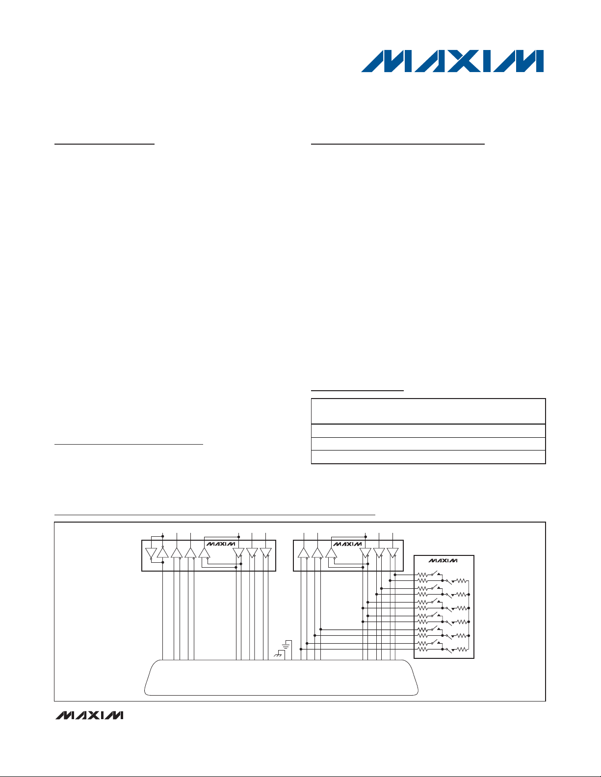
Typical Operating Circuit
19-4595; Rev 1; 7/09
For pricing, delivery, and ordering information, please contact Maxim Direct at 1-888-629-4642,
or visit Maxim’s website at www.maxim-ic.com.
+
Denotes a lead(Pb)-free/RoHS-compliant package.
*
EP = Exposed pad.
PART TEMP RANGE
PINPACKAGE
MAX13171EETU+ - 40°C to + 85°C 38 TQFN-EP*
MAX13173EETU+ - 40°C to + 85°C 38 TQFN-EP*
MAX13175EETU+ - 40°C to + 85°C 38 TQFN-EP*
Data Networking
PCI Cards
CSU and DSU
Telecommunication
Equipment
Data Routers
Data Switches
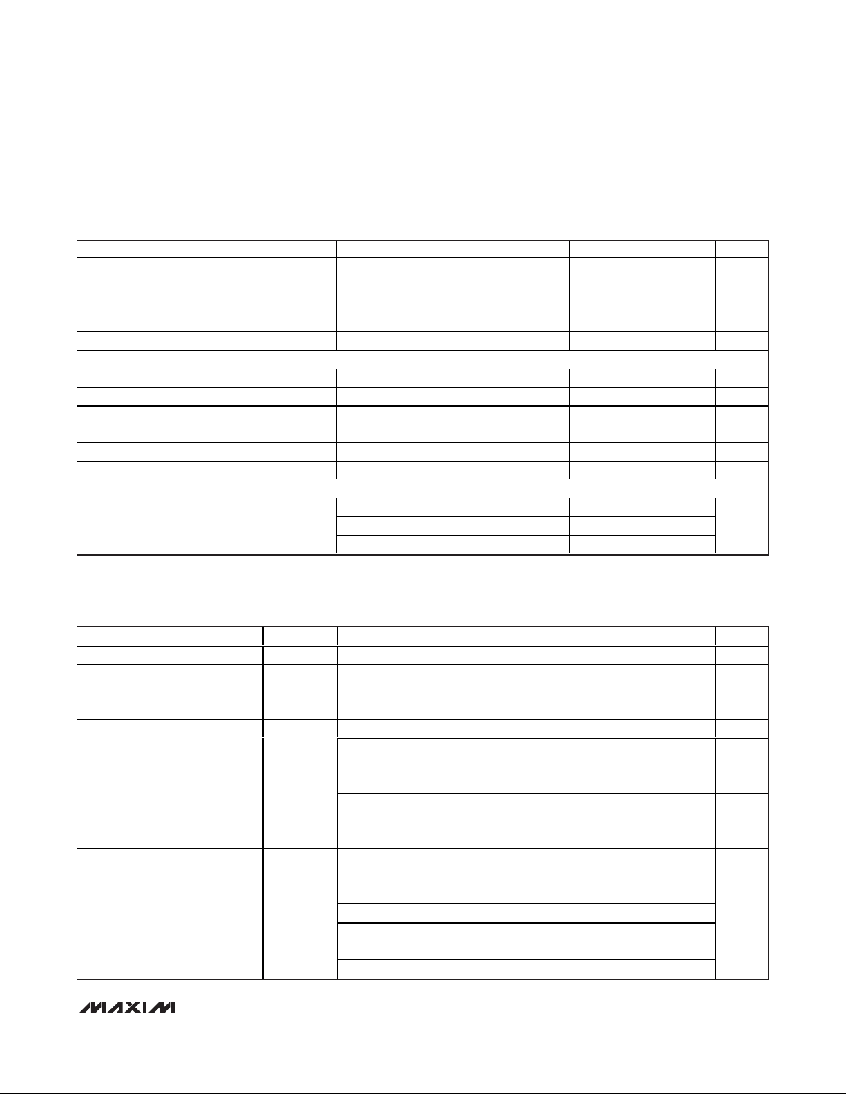
CTS DSR RTSDTRDCD
LL
RXD RXC TXDTXC SCTE
T4
R4
13
18 5 10 8 22 6 23 20 19 4 1 7 16 3 9 17 12 15 11 24 14 2
CTS A (106)
CTS B
LL A (141)
R2R3
DSR A (109)
DSR B
R1
MAX13173E
T3
DCD A (107)
DCD B
DTR A (108)
DTR B
T1T2
RTS A (105)
RTS B
DB-25 CONNECTOR
SG (102)
SHIELD (101)
RXD A (104)
RXD B
R2R3
RXC B
RXC A (115)
R1
MAX13171E
T3
TXC A (114)
TXC B
SCTE A (113)
SCTE B
T1T2
TXD B
TXD A (103)
MAX13175E
Page 2
MAX13171E/MAX13173E/MAX13175E
Multiprotocol, Pin-Selectable
Data Interface Chipset
2 _______________________________________________________________________________________
ABSOLUTE MAXIMUM RATINGS
MAX13171E ELECTRICAL CHARACTERISTICS
(VCC= +3.135V to +5.5V, VL= +1.62V to +5.5V, C1 = C2 = 1µF, C3 = C4 = C5 = 4.7µF (Figure 15), TA= -40°C to +85°C, unless otherwise noted. Typical values are at V
CC
= +3.3V, VL= +1.8V, TA= +25°C.) (Note 2)
Stresses beyond those listed under “Absolute Maximum Ratings” may cause permanent damage to the device. These are stress ratings only, and functional
operation of the device at these or any other conditions beyond those indicated in the operational sections of the specifications is not implied. Exposure to
absolute maximum rating conditions for extended periods may affect device reliability.
Note 1: Package thermal resistances were obtained using the method described in JEDEC specification JESD51-7, using a four-layer
board. For detailed information on package thermal considerations, refer to http://www.maxim-ic.com/thermal-tutorial
.
(All voltages to GND, unless otherwise noted.)
Supply Voltages
V
CC
........................................................................ -0.3V to +6V
V
L
........................................................................... -0.3V to +6V
V
EE
..................................................................... +0.3V to -7.1V
V
DD
.................................................................... -0.3V to +7.1V
V
DD
to VCC............................................................-0.3V to +6V
Logic-Input Voltages
M0, M1, M2, DCE/DTE, LATCH, INVERT, T_IN ..... -0.3V to +6V
Termination Network Inputs
R_A, R_B, R_C.......................................................-15V to +15V
R_A to R_B (only for high-Z state) .....................................±14V
R_A to R_B...........................................................................±6V
R_A to R_C (only for high-Z state) .....................................±14V
R_A to R_C...........................................................................±3V
R_B to R_C (only for high-Z state) .......................................±3V
Logic-Output Voltages
R_OUT ........................................................-0.3V to (V
L
+ 0.3V)
Transmitter Outputs
T_OUT_, T_OUT_/R_IN_
(no-cable, V.28, V.10 modes) ...............................-15V to +15V
Short-Circuit Duration to GND..................................Continuous
Receiver Inputs
R_IN_, T_OUT_/R_IN ............................................-15V to +15V
R_INA to R_INB, T3OUTA/R3INA
to T3OUTB/R3INB ................................................-15V to +15V
Continuous Power Dissipation (T
A
= +70°C)
38-Pin TQFN (derate 35.7mW/°C above +70°C) ........2857mW
Junction-to-Case Thermal Resistance (θ
JC
) (Note 1)
38-Pin TQFN ....................................................................1°C/W
Junction-to-Ambient Thermal Resistance (θ
JA
) (Note 1)
38-Pin TQFN ..................................................................28°C/W
Operating Temperature Range ...........................-40°C to +85°C
Junction Temperature......................................................+150°C
Storage Temperature Range ............................-65°C to +150°C
Lead Temperature (soldering, 10s) ................................+300°C
VCC Operating Range V
VL Operating Range V
VL Supply Current I
PARAMETER SYMBOL CONDITIONS MIN TYP MAX UNITS
VCC Supply Current (DCE Mode)
(Digital Inputs = GND or V
(Transmitter Outputs Static)
Internal Power Dissipation
(DCE Mode)(Static)
CC
)
CC
L
L
I
CC
P
All inputs connected to GND, all receiver
outputs low, V
RS-530, RS-530A, X.21, V.36/RS-449
mode (V.11), no load
RS-530, RS-530A, X.21, V.36/RS-449
mode (V.11), full load
V.35 mode, no load 21 38 mA
V.35 mode, full load 150 210 mA
V.28 mode, no load 15 30 mA
V.28 mode, full load 28 42 mA
No-cable mode 0.01 10 µA
RS-530, RS-530A, X.21, V.36/RS-449
mode (V.11), full load
D
V.35 mode, full load 500
V.28 mode, full load 70
= +5.5V
L
3.135 5.5 V
1.62 V
550 800 µA
15 28 mA
150 200 mA
100
CC
V
mW
Page 3
MAX13171E/MAX13173E/MAX13175E
Multiprotocol, Pin-Selectable
Data Interface Chipset
_______________________________________________________________________________________ 3
MAX13171E ELECTRICAL CHARACTERISTICS (continued)
(VCC= +3.135V to +5.5V, VL= +1.62V to +5.5V, C1 = C2 = 1µF, C3 = C4 = C5 = 4.7µF (Figure 15), TA= -40°C to +85°C, unless otherwise noted. Typical values are at V
CC
= +3.3V, VL= +1.8V, TA= +25°C.) (Note 2)
PARAMETER SYMBOL CONDITIONS MIN TYP MAX UNITS
Positive Charge-Pump Output
Voltage
Negative Charge-Pump Output
Voltage
Charge-Pump Enable Time
Thermal Shutdown Protection THSD +145 °C
LOGIC INPUTS (M0, M1, M2, DCE/DTE, T1IN, T2IN, T3IN)
Input High Voltage V
Input Low Voltage V
Logic-Input Current I
Pullup Resistor R
LOGIC OUTPUTS (R1OUT, R2OUT, R3OUT)
Output High Voltage V
Output Low Voltage V
Output Pullup Resistor R
V.11 TRANSMITTER
Open-Circuit Differential Output
Voltage
Loaded Differential Output
Voltage
Change in Magnitude of Output
Differential Voltage
Common-Mode Output Voltage V
Change in Magnitude of
Common-Mode Output Voltage
Short-Circuit Current I
Rise Time t
Fall Time t
V.28, V.35 modes, no load (Note 3) 5.93 7.1
V.28 mode, full load (Note 3) 5.6 5.86
V.35 mode, full load (Note 3) 4.6 5.1
RS - 530, RS - 530A, X .21, V .36/RS - 449 m od e
( V .11) ( N ote 3)
No-cable mode V
V.28, V.35 modes, no load (Note 3) -5.89
V.28 mode, full load (Note 3) -5.74 -5.4
V.35 mode, full load, Note 3 -4.46 -3.8
RS - 530, RS - 530A, X .21, V .36/RS - 449 m od e
( V .11) ( N ote 3)
No-cable mode 0
Time until all V
meet
T1IN, T2IN, T3IN -1 +1 µA
M0, M1, M2, DCE/DTE to V
I
I
No-cable mode (to VL) 71.4 kΩ
Open circuit, R = 1.95kΩ, Figure 1 -V
R = 50Ω, Figure 1
R = 50Ω, Figure 1 I2I
| R = 50Ω, Figure 1 0.2 V
R = 50Ω, Figure 1 3.0 V
| R = 50Ω, Figure 1 (Note 3) 0.2 V
V
Figures 2, 6 4.5 ns
Figures 2, 6 6.5 ns
= 4mA 0.66 x V
SOURCE
= 4mA 0.33 x V
SINK
= GND 150 mA
OUT
and VEE specifications
DD
V
V
|∆V
|∆V
V
DD
V
EE
IH
IN
PUIN
OH
OL
PUY
ODO
ODL
OC
SC
IL
OD
OC
r
f
V
4.9 5.26 5.7
CC
V
-4.84 -4.47 -4.16
< 1 ms
0.66 x V
L
L
0.33 x V
50 100 170 kΩ
L
+V
CC
0.5 x
V
ODO
CC
V
V
L
V
V
L
V
V
Page 4
MAX13171E/MAX13173E/MAX13175E
Multiprotocol, Pin-Selectable
Data Interface Chipset
4 _______________________________________________________________________________________
MAX13171E ELECTRICAL CHARACTERISTICS (continued)
(VCC= +3.135V to +5.5V, VL= +1.62V to +5.5V, C1 = C2 = 1µF, C3 = C4 = C5 = 4.7µF (Figure 15), TA= -40°C to +85°C, unless otherwise noted. Typical values are at V
CC
= +3.3V, VL= +1.8V, TA= +25°C.) (Note 2)
PARAMETER SYMBOL CONDITIONS MIN TYP MAX UNITS
Transmitter Input to Output
Propagation Delay (Figures 2, 6)
Data Skew |t
Channel-to-Channel Skew t
V.11 RECEIVER
Differential Threshold Voltage V
Input Hysteresis ∆V
Receiver Input Current I
Receiver Input Resistance R
Rise or Fall Time tr, t
Receiver Input to Output Delay t
Data Skew |t
Channel-to-Channel Skew t
V.35 TRANSMITTER
Differential Output Voltage V
Output High Current I
Output Low Current I
Output Leakage Current I
Rise or Fall Time tr, t
Transmitter Input to Output Delay t
Data Skew |t
Channel-to-Channel Skew t
V.35 RECEIVER
Differential Threshold Voltage V
Input Hysteresis ∆V
Receiver Input Current I
Receiver Input Resistance R
Rise or Fall Time tr, t
Receiver Input to Output Delay t
Data Skew |t
Channel-to-Channel Skew t
V.28 TRANSMITTER
Output-Voltage Swing |VOD|
Short-Circuit Current I
t
, t
PHL
PHL-tPLH
SKEW
TH
TH
IN
IN
, t
PHL
PHL-tPLH
SKEWR
OD
OH
OL
Z
PLH, tPHL
PLH - tPHL
SKEWR
TH
TH
IN
IN
, t
PHL
- t
PHL
SKEWR
Figures 2, 6 22 28
PLH
VL ≥ +3V, Figures 2, 6 20 25
| Figures 2, 6 (Note 3) 2 ns
Figures 2, 6 (Notes 3, 4) 3 ns
-7V ≤ VCM ≤ +7V -200 -50 mV
-7V ≤ VCM ≤ +7V 15 mV
-10V ≤ V
-10V ≤ V
Figures 2, 7 3 ns
f
Figures 2, 7 2.5 ns
PLH
≤ +10V -0.66 +0.66 mA
A,B
≤ +10V 15 30 kΩ
A,B
| Figures 2, 7 (Note 3) 3 ns
Figures 2, 7 (Notes 3, 4) 3 ns
Full load, -4V < VCM < +4V, Figure 3 ±0.44 ±0.55 ±0.66 V
V
= 0V -13 -11 -9 mA
A,B
V
= 0V 9 11 13 mA
A,B
-0.25V ≤ V
≤ +0.25V, power off or
OUT
no-cable mode
Figures 3, 6 5 ns
f
Figures 3, 6 19 35 ns
| Figures 3, 6 (Note 3) 3 ns
Figures 3, 6 (Notes 3, 4) 3 ns
-2V ≤ VCM ≤ +2V -200 -50 mV
-2V ≤ VCM ≤ +2V 15 mV
-10V ≤ V
-10V ≤ V
Figures 3, 7 3 ns
f
Figures 3, 7 25 ns
PLH
| Figures 3, 7 (Note 3) 3 ns
PLH
≤ +10V -0.66 +0.66 mA
A,B
≤ +10V 15 30 kΩ
A,B
Figures 3, 7 (Notes 3, 4) 3 ns
Open circuit 7.1
R
= 3kΩ 56
L
OH
±0.05 ±5 µA
85 mA
ns
V
Page 5
MAX13171E/MAX13173E/MAX13175E
Multiprotocol, Pin-Selectable
Data Interface Chipset
_______________________________________________________________________________________ 5
MAX13171E ELECTRICAL CHARACTERISTICS (continued)
(VCC= +3.135V to +5.5V, VL= +1.62V to +5.5V, C1 = C2 = 1µF, C3 = C4 = C5 = 4.7µF (Figure 15), TA= -40°C to +85°C, unless otherwise noted. Typical values are at V
CC
= +3.3V, VL= +1.8V, TA= +25°C.) (Note 2)
MAX13173E ELECTRICAL CHARACTERISTICS
(VCC= +3.135V to +5.5V, VL= +1.62V to +5.5V, C1 = C2 = 1µF, C3 = C4 = C5 = 4.7µF (Figure 15), TA= -40°C to +85°C, unless
otherwise noted. Typical values are at V
CC
= +3.3V, VL= +1.8V, TA= +25°C.) (Note 2)
Output Leakage Current I
Output Slew Rate SR
Transmitter Input to Output Delay t
V.28 RECEIVER
Input Threshold Low V
Input Threshold High V
Input Hysteresis V
Input Resistance R
Rise or Fall Time tr, t
Receiver Input to Output Delay t
ESD PROTECTION
T_OUT, T3OUT_/R1IN_, R_IN to
GND
PARAMETER SYMBOL CONDITIONS MIN TYP MAX UNITS
Z
R/F
, t
PHL
PLHRL
IL
IH
HYST
IN
f
PHL, tPLH
-0.25V ≤ V
no-cable mode
RL = 3kΩ, CL = 2500pF (swing in ±3V),
Figures 4, 10
= 3kΩ, CL = 2500pF, Figures 4, 10 1 2 µs
-15V ≤ VIN ≤ +15V 3 5 7 kΩ
Figures 5, 11 3 ns
Figures 5, 11 150 ns
Human Body Model ±15
Air Gap Discharge IEC 61000-4-2 ±12
Contact Discharge IEC 61000-4-2 ±8
≤ +0.25V, power off or
OUT
±0.05 ±5 µA
4 30 V/µs
0.8 1.2 V
1.2 2 V
0.25 V
kV
PARAMETER SYMBOL CONDITIONS MIN TYP MAX UNITS
VCC Operating Range V
VL Operating Range V
VL Supply Current I
VCC Supply Current I
Internal Power Dissipation P
Positive Charge-Pump Output
Voltage
CC
L
L
CC
V
DD
All inputs connected to GND, all receiver
outputs low, V
RS-530A, no load 11 21 mA
RS-530, X.21, V.36/RS-449, DCE mode,
INVERT = low, full load, transmitter outputs
static, digital inputs = GND or V
V.28 mode, no load 21 38 mA
V.28 mode, full load 42 65 mA
No-cable mode 0.01 10 µA
RS-530, X.21, V.36/RS-449; DCE mode,
D
INVERT = low, full load
V.28 mode, no load (Note 3) 5.9 7.1
V.28 mode with full load (Note 3) 5.6 5.79
RS-530 mode, full load (Note 3) 4.84 5.15 5.5
RS-530A mode, full load 5.15
No-cable mode V
= +5.5V
L
3.135 5.5 V
1.62 V
680 1100 µA
41 210 mA
L
120 mW
CC
CC
V
V
Page 6
MAX13171E/MAX13173E/MAX13175E
Multiprotocol, Pin-Selectable
Data Interface Chipset
6 _______________________________________________________________________________________
MAX13173E ELECTRICAL CHARACTERISTICS (continued)
(VCC= +3.135V to +5.5V, VL= +1.62V to +5.5V, C1 = C2 = 1µF, C3 = C4 = C5 = 4.7µF (Figure 15), TA= -40°C to +85°C, unless
otherwise noted. Typical values are at V
CC
= +3.3V, VL= +1.8V, TA= +25°C.) (Note 2)
PARAMETER SYMBOL CONDITIONS MIN TYP MAX UNITS
Negative Charge-Pump Output
Voltage
Thermal Shutdown Protection THSD +145 °C
Charge-Pump Enable Time
LOGIC INPUTS (M0, M1, M2, DCE/DTE, INVERT, T1IN, T2IN, T3IN, T4IN, T5IN/R5OUT)
Input High Voltage V
Input Low Voltage V
Logic-Input Current I
Pullup Resistor R
LOGIC OUTPUTS (R1OUT, R2OUT, R3OUT, R4OUT, T5IN/R5OUT)
Output High Voltage V
Output Low Voltage V
Output Pullup Resistor R
V.11 TRANSMITTER (T1, T2, T3)
Open-Circuit Differential Output
Voltage
Loaded Differential Output
Voltage
V.28 mode, no load (Note 3) -5.83
V.28 mode with full load (Note 3) -5.55 -5.3
V
EE
RS-530 mode, full load (Note 3) -4.71 -4.44 -4.17
RS-530A mode, full load -4.44
No-cable mode 0
Time until all V
and VEE specifications
DD
meet
IH
IL
T1IN, T2IN, T3IN, T4IN -1 +1 µA
M0, M1, M2, DCE/DTE, INVERT to V
I
I
= 4mA 0.66 x V
SOURCE
= 4mA 0.33 x V
SINK
No-cable mode (to VL) 71.4 kΩ
Open circuit, R = 1.95kΩ, Figure 1 -V
V
IN
PUIN
OH
OL
PUY
ODO
R = 50Ω, Figure 1
V
ODL
R = 50Ω, Figure 1 |2|
V
< 1 ms
0.66 x V
L
0.33 x V
L
50 100 170 kΩ
L
CC
+V
CC
V
V
L
V
V
L
V
0.5 x
V
ODO
V
Change in Magnitude of Output
Differential Voltage
Common-Mode Output Voltage V
Change in Magnitude of
Common-Mode Output Voltage
Short-Circuit Current I
Output Leakage Current I
Rise Time t
Fall Time t
Transmitter Input to Output Prop
Delay
Data Skew |t
Channel-to-Channel Skew t
| R = 50Ω, Figure 1 0.2 V
|∆V
OD
R = 50Ω, Figure 1 3.0 V
| R = 50Ω, Figure 1 (Note 3) 0.2 V
V
= GND 150 mA
OUT
-0.25V ≤ V
≤ +0.25V, power-off or no-
OUT
cable mode
Figures 2, 6 4 10 ns
Figures 2, 6 6 10 ns
Figures 2, 6 20 28 ns
PLH
Figures 2, 6, VL ≥ +3V 25 ns
| Figures 2, 6 (Note 3) 2 ns
PLH
Figures 2, 6 (Notes 3, 4) 3 ns
t
PHL
PHL
|∆V
SC
SKEW
OC
OC
Z
r
f
, t
- t
±0.05 ±5 µA
Page 7
MAX13171E/MAX13173E/MAX13175E
Multiprotocol, Pin-Selectable
Data Interface Chipset
_______________________________________________________________________________________ 7
MAX13173E ELECTRICAL CHARACTERISTICS (continued)
(VCC= +3.135V to +5.5V, VL= +1.62V to +5.5V, C1 = C2 = 1µF, C3 = C4 = C5 = 4.7µF (Figure 15), TA= -40°C to +85°C, unless
otherwise noted. Typical values are at V
CC
= +3.3V, VL= +1.8V, TA= +25°C.) (Note 2)
PARAMETER SYMBOL CONDITIONS MIN TYP MAX UNITS
V.11 RECEIVER (R1, R2, R3)
Differential Threshold Voltage V
Input Hysteresis ∆V
Receiver Input Current I
Receiver Input Resistance R
Rise or Fall Time tr, t
Receiver Input to Output Delay t
Data Skew |t
Channel-to-Channel Skew t
V.10 TRANSMITTER (T2, T4, T5)
Open-Circuit Output Voltage
Swing
Output-Voltage Swing V
Short-Circuit Current I
Output Leakage Current I
Rise or Fall Time tr, t
Transmitter Input to Output Delay t
V.10 RECEIVER (R2, R4, R5)
Input Threshold Voltage V
Input Hysteresis ∆V
Receiver Input Current I
Receiver Input Resistance R
Rise or Fall Time tr, t
Receiver Input to Output Delay
Data Skew |t
V.28 TRANSMITTER (All CHANNELS)
Output-Voltage Swing |VOD|
Short-Circuit Current I
Output Leakage Current I
-7V ≤ VCM ≤ +7V -200 -50 mV
-7V ≤ VCM ≤ +7V 15 mV
-10V ≤ V
-10V ≤ V
Figures 2, 7 3 ns
f
Figures 2, 7 27 ns
PLH
| Figures 2, 7 (Note 3) 3 ns
PLH
≤ +10V -0.66 +0.66 mA
A,B
≤ +10V 15 30 kΩ
A,B
Figures 2, 7 (Notes 3, 4) 3 ns
RL = 3.9kΩ (out high) 4 6
RL = 3.9kΩ (out low) -6 -4
PHL
PHL
SKEWR
V
TH
TH
IN
IN
, t
- t
O
RL = 450Ω (out high) 3.6
T
RL = 450Ω (out low) -3.6
RL = 450Ω
SC
Z
PLH, tPHLRL
TH
TH
IN
IN
t
PLH
t
PHL
- t
PHL
VO = GND -55 +55 mA
-0.25V ≤ V
≤ +0.25V, power-off or
OUT
no-cable mode
RL = 450Ω, CL = 100pF, Figure 8 2 µs
f
= 450Ω, CL = 100pF, Figure 8 1 µs
-10V ≤ VA ≤ +10V -0.66 +0.66 mA
-10V ≤ VA ≤ +10V 15 30 kΩ
Figures 5, 9 3 ns
f
Figure 9 55
Figure 9 109
| Figures 5, 9 (Note 3) 60 ns
PLH
Open circuit 7.1
= 3kΩ 56
R
L
OH
Z
-0.25V ≤ V
no-cable mode
≤ +0.25V, power-off or
OUT
0.9 x
|
|V
O
±0.05 +5 µA
50 250 mV
25 mV
90 mA
±0.05 ±5 µA
V
V
ns
V
Page 8
MAX13171E/MAX13173E/MAX13175E
Multiprotocol, Pin-Selectable
Data Interface Chipset
8 _______________________________________________________________________________________
MAX13173E ELECTRICAL CHARACTERISTICS (continued)
(VCC= +3.135V to +5.5V, VL= +1.62V to +5.5V, C1 = C2 = 1µF, C3 = C4 = C5 = 4.7µF, Figure 15, TA= -40°C to +85°C, unless
otherwise noted. Typical values are at V
CC
= +3.3V, VL= +1.8V, TA= +25°C.) (Note 2)
MAX13175E ELECTRICAL CHARACTERISTICS (continued)
(VCC= +3.135V to +5.5V, VL= +1.62V to +5.5V, C1 = C2 = 1µF, C3 = C4 = C5 = 4.7µF, Figure 15, TA= -40°C to +85°C, unless
otherwise noted. Typical values are at V
CC
= +3.3V, VL= +1.8V, TA= +25°C.) (Note 2)
PARAMETER SYMBOL CONDITIONS MIN TYP MAX UNITS
Output Slew Rate SR
Transmitter Input to Output Delay t
V.28 RECEIVER (All CHANNELS)
Input Threshold Low V
Input Threshold High V
Input Hysteresis V
Input Resistance R
Rise or Fall Time tr, t
Receiver Input to Output Delay t
ESD PROTECTION
T_OUT, T_OUT/R_IN_, R_IN
R/F
, t
PHL
IL
IH
HYST
IN
PHL, tPLH
RL = 3kΩ, CL = 2500pF (swing in ±3V)
Figures 4, 10
PLHRL
f
= 3kΩ, CL = 2500pF, Figures 4, 10 1 2 µs
-15V ≤ VIN ≤ +15V 3 5 7 kΩ
Figures 5, 11 3 ns
Figures 5, 11 150 ns
Human Body Model ±15
Air Gap Discharge IEC 61000-4-2 ±15
Contact Discharge
4 30 V/µs
0.8 1.2 V
1.2 2 V
0.25 V
kV
±5
PARAMETER SYMBOL CONDITIONS MIN TYP MAX UNITS
VCC Operating Range V
VL Operating Range V
VDD Operating Range V
VEE Operating Range V
VL POR Rising Threshold 0.7 1.06 1.46 V
VCC POR Rising Threshold 1 1.88 2.75 V
VDD Supply Current I
VCC Supply Current
VL Supply Current I
VEE Supply Current I
TERMINATOR INPUTS
Differential-Mode Impedance
V.35 Mode
Common-Mode Impedance V.35
Mode
CC
L
DD
EE
DD
I
CC
I
CC_NOCABVEE
EE
All inputs connected to GND or VL, except
no-cable mode
All inputs connected to GND or VL, except
no-cable mode
= 0V, M[x] = 1111 (Note 5) 1.29 2.6 mA
All inputs connected to GND or V
L
All inputs connected to GND or V
-2V ≤ V
-2V ≤ V
≤ +2V, all channels, Figure 12 90 104 110 Ω
CM
≤ +2V, all channels, Figure 13 135 153 165 Ω
CM
3.135 5.5 V
1.62 V
4.5 7.1 V
-7.1 -4 V
0.05 0.25 mA
2.15 5.9 mA
L
L
-1 +1 µA
-3.5 -1 mA
CC
V
Page 9
MAX13171E/MAX13173E/MAX13175E
Multiprotocol, Pin-Selectable
Data Interface Chipset
_______________________________________________________________________________________ 9
Note 2: All devices are 100% production tested at TA= +85°C for the MAX13171E/MAX13173E and TA= +25°C for the
MAX13175E. Specifications over temperature are guaranteed by design.
Note 3: Guaranteed by design, not production tested.
Note 4: Output-to-output skews are evaluated as difference of propagation delays between different channels in the same condition
and for the same polarity (LH or HL).
Note 5: M[x] is the input bus DTE/DCE, M2, M1, M0.
MAX13175E ELECTRICAL CHARACTERISTICS (continued)
(VCC= +3.135V to +5.5V, VL= +1.62V to +5.5V, C1 = C2 = 1µF, C3 = C4 = C5 = 4.7µF, Figure 15, TA= -40°C to +85°C, unless
otherwise noted. Typical values are at V
CC
= +3.3V, VL= +1.8V, TA= +25°C.) (Note 2)
PARAMETER SYMBOL CONDITIONS MIN TYP MAX UNITS
Differential-Mode Impedance
V.11 Mode
Differential Path Enable Time 50 µs
Differential Path Disable Time 300 µs
Common-Mode Path Enable Time 12 µs
Common-Mode Path Disable
Time
High-Impedance Leakage
Current
LOGIC INPUTS (M0, M1, M2, LATCH, DCE/DTE)
Input High Voltage V
Input Low Voltage V
Logic Input Current I
ESD PROTECTION
All Other Pins Human Body Model ±2 kV
-7V ≤ VCM ≤ +7V, all channels, except nocable mode, Figure 12
-7V ≤ V
V
AB
I
IN
-15V ≤ V
Z
IH
IL
VIN = GND or V
Human Body Model ±15
Air Gap Discharge IEC 61000-4-2 ±10R_A, R_B to GND
Contact Discharge IEC 61000-4-2 ±6
≤ +7V, no cable, VEE = 0V,
CM
< 2V, Figure 12
≤ +15V -50 +50 µA
R_A
L
100 104 110
115
2µs
0.66 x V
L
0.33 x V
-1 +1 µA
L
Ω
V
V
kV
Page 10
MAX13171E/MAX13173E/MAX13175E
Multiprotocol, Pin-Selectable
Data Interface Chipset
10 ______________________________________________________________________________________
MAX13171E Typical Operating Characteristics
(VCC= +3.3V, VL= +1.8V, TA= +25°C, unless otherwise noted.)
V.28 SUPPLY CURRENT
vs. DATA RATE
MAX13171E toc02
DATA RATE (kbps)
SUPPLY CURRENT (mA)
20015050 100
10
20
30
40
60
50
70
80
0
0250
DCE MODE, ALL TRANSMITTERS
OPERATING AT THE SPECIFIED
DATA RATE, R
L
= 3kΩ, CL = 2500pF
RS-530 SUPPLY CURRENT
350
DCE MODE, R = 50Ω,
ALL TRANSMITTERS
300
OPERATING AT THE
SPECIFIED DATA RATE
250
vs. DATA RATE
MAX13171E toc01
V.35 SUPPLY CURRENT
350
DCE MODE, FULLY LOADED,
ALL TRANSMITTERS
300
OPERATING AT THE
SPECIFIED DATA RATE
250
vs. DATA RATE
MAX13171E toc03
200
150
SUPPLY CURRENT (mA)
100
50
0
0.1 10,000
DATA RATE (kbps)
V.11 DIFFERENTIAL OUTPUT VOLTAGE
vs. TEMPERATURE
3
2
1
0
DC OUTPUT
DCE MODE,
R = 50Ω
-1
-2
DIFFERENTIAL OUTPUT VOLTAGE (V)
-3
-40 85
TEMPERATURE (°C)
100010
V.28 OUTPUT VOLTAGE
vs. TEMPERATURE
8
V
OUT+
V
OUT-
603510-15
MAX13171E toc04
6
4
2
DC OUTPUT
0
DCE MODE,
= 3kΩ
R
L
-2
OUTPUT VOLTAGE (V)
-4
-6
-8
-40 85
V
OUT+
V
OUT-
TEMPERATURE (°C)
6035-15 10
V.35 LOADED DIFFERENTIAL OUTPUT
VOLTAGE vs. COMMON-MODE VOLTAGE
560
DC OUTPUT
555
550
545
540
535
DIFFERENTIAL OUTPUT VOLTAGE (mV)
530
-4 4
|VOD|
-2 0 2
COMMON-MODE VOLTAGE (V)
MAX13171E toc07
V.11/V.35 RECEIVER INPUT CURRENT
vs. INPUT VOLTAGE
500
DC OUTPUT
400
DTE MODE
300
200
100
0
-100
INPUT CURRENT (µA)
-200
-300
-400
-500
-10 104-4-6 6
INPUT VOLTAGE (V)
R1INA
R2INA, R3INA
80-2 2-8
200
150
SUPPLY CURRENT (mA)
100
50
0
600
400
MAX13171E toc05
200
0
-200
OUTPUT VOLTAGE (V)
-400
-600
2.5
2.0
1.5
MAX13171E toc08
1.0
0.5
0
-0.5
INPUT CURRENT (mA)
-1.0
-1.5
-2.0
-2.5
0.1 10,000
DATA RATE (kbps)
100010
V.35 OUTPUT VOLTAGE
vs. TEMPERATURE
V
OH
DC OUTPUT
DCE MODE,
= 0V, FULL LOAD
V
CM
V
OL
-40 85
TEMPERATURE (°C)
6035-15 10
V.28 RECEIVER INPUT CURRENT
vs. INPUT VOLTAGE
DC OUTPUT
DTE MODE
-10 104-4-6 6
INPUT VOLTAGE (V)
80-2 2-8
MAX13171E toc06
MAX13171E toc09
Page 11
MAX13171E/MAX13173E/MAX13175E
Multiprotocol, Pin-Selectable
Data Interface Chipset
______________________________________________________________________________________
11
MAX13171E Typical Operating Characteristics (continued)
(VCC= +3.3V, VL= +1.8V, TA= +25°C, unless otherwise noted.)
V.11 LOOPBACK OPERATION (40Mbps)
MAX13171E toc10
10ns/div
R_OUT
2V/div
T_OUT_/R_IN_
2V/div
T_IN
2V/div
R = 50Ω
V.28 LOOPBACK OPERATION (250kbps)
MAX13171E toc11
1µs/div
R_OUT
2V/div
T_OUT_/R_IN_
5V/div
T_IN
2V/div
RL = 3kΩ, CL = 2500pF
V.35 LOOPBACK OPERATION (40Mbps)
FULL LOAD
T_IN
2V/div
MAX13171E toc12
V.28 SLEW RATE vs.
35
30
25
LOAD CAPACITANCE
Ω
RL = 3k
MAX13171E toc13
T_OUT_/R_IN_
0.5V/div
R_OUT
2V/div
V.11/V.35 RECEIVER PROPAGATION
DELAY vs. TEMPERATURE
20
18
16
14
12
10
8
6
PROPAGATION DELAY (ns)
4
2
0
-40 8560-15
t
PHL
10 35
TEMPERATURE (°C)
1µs/div
t
PLH
25
20
MAX13171E toc14
15
10
PROPAGATION DELAY (ns)
5
0
-40 8560-15
V.11 TRANSMITTER PROPAGATION
DELAY vs. TEMPERATURE
t
PLH
t
PHL
10 35
TEMPERATURE (°C)
SLEW RATE (V/µs)
20
15
10
5
0
0500040001000
30
25
MAX13171E toc15
20
15
10
PROPAGATION DELAY (ns)
SR
F
SR
R
2000 3000
LOAD CAPACITANCE (pF)
V.35 TRANSMITTER PROPAGATION
DELAY vs. TEMPERATURE
t
PHL
t
PLH
5
0
-40 8560-15
10 35
TEMPERATURE (°C)
MAX13171E toc16
Page 12
MAX13171E/MAX13173E/MAX13175E
Multiprotocol, Pin-Selectable
Data Interface Chipset
12 ______________________________________________________________________________________
MAX13173E Typical Operating Characteristics
(VCC= +3.3V, VL= +1.8V, TA= +25°C, unless otherwise noted.)
V.28 SUPPLY CURRENT
vs. DATA RATE
MAX13171E toc18
DATA RATE (kbps)
SUPPLY CURRENT (mA)
200100 15050
10
20
30
40
50
60
70
80
90
0
0250
DCE MODE, INVERT = 1
ALL TRANSMITTERS
OPERATING AT THE
SPECIFIED DATA RATE
FULL LOAD, RL = 50Ω,
C
L
= 2500pF
NO LOAD
V.11 DIFFERENTIAL OUTPUT VOLTAGE
vs. TEMPERATURE
MAX13171E toc19
TEMPERATURE (°C)
DIFFERENTIAL OUTPUT VOLTAGE (V)
6035-15 10
-3
-2
-1
0
2
1
3
4
-4
-40 85
DC OUTPUT
DCE MODE,
INVERT = 1,
R = 50Ω
V
OUT+
V
OUT-
V.10 OUTPUT VOLTAGE
vs. TEMPERATURE
MAX13171E toc20
TEMPERATURE (°C)
OUTPUT VOLTAGE (V)
6035-15 10
-6
-4
-2
0
4
2
6
8
-8
-40 85
DC OUTPUT
DCE MODE
V
OUT+
RL = 3.9kΩ
RL = 3.9kΩ
RL = 450Ω
V
OUT-
V.28 OUTPUT VOLTAGE
vs. TEMPERATURE
MAX13171E toc21
TEMPERATURE (°C)
OUTPUT VOLTAGE (V)
6035-15 10
-6
-4
-2
0
4
2
6
8
-8
-40 85
DC OUTPUT
DCE MODE,
R
L
= 3kΩ
V
OUT+
V
OUT-
V.11 RECEIVER INPUT CURRENT
vs. INPUT VOLTAGE
MAX13171E toc22
INPUT VOLTAGE (V)
INPUT CURRENT (µV)
62-6 -2
-400
-300
-200
0
200
100
300
-100
400
500
-500
-10 1040-8 -4 8
DC OUTPUT
DCE MODE
R3INA
R2INA
R1INA
R-530 SUPPLY CURRENT
vs. DATA RATE
MAX13171E toc17
DATA RATE (kbps)
SUPPLY CURRENT (mA)
10 1000
50
100
150
200
250
0
0 100,000
DCE MODE, INVERT = 1
3 TRANSMITTERS OPERATING
AT THE SPECIFIED DATA RATE
IN V.11 MODE
FULL LOAD, R = 50
Ω
NO LOAD, R = 1.95k
Ω
INPUT CURRENT (mA)
V.28 RECEIVER INPUT CURRENT
vs. INPUT VOLTAGE
4
DC OUTPUT
3
2
1
0
-1
-2
-3
-4
-15 15010-10
-5 5
INPUT VOLTAGE (V)
MAX13171E toc23
Page 13

MAX13171E/MAX13173E/MAX13175E
Multiprotocol, Pin-Selectable
Data Interface Chipset
______________________________________________________________________________________
13
MAX13173E Typical Operating Characteristics (continued)
(VCC= +3.3V, VL= +1.8V, TA= +25°C, unless otherwise noted.)
SLEW RATE (V/µs)
35
30
25
20
15
10
5
0
0 500040001000
V.28 SLEW RATE vs.
LOAD CAPACITANCE
RL = 3k
Ω
SR
R
LOAD CAPACITANCE (pF)
V.28 LOOPBACK OPERATION (250kbps)
T_IN
2V/div
SR
F
2000 3000
RL = 3kΩ, CL = 2500pF
MAX13171E toc24
RISE/FALL TIME (µs)
MAX13171E toc27
V.10 TRANSMITTER RISE/FALL
TIME vs. LOAD CAPACITANCE
2.0
1.8
1.6
1.4
1.2
1.0
0.8
0.6
0.4
0.2
0
0 500040001000
LOAD CAPACITANCE (pF)
FALL
RISE
2000 3000
V.11 LOOPBACK OPERATION (40Mbps)
FULL LOAD
T_IN
MAX13171E toc25
2V/div
T_OUT_/R_IN_
2V/div
R_OUT
2V/div
V.10 LOOPBACK OPERATION (100kbps)
T_IN
2V/div
MAX13171E toc26
10ns/div
MAX13171E toc28
RL = 3.9kΩ
T_OUT_/R_IN_
5V/div
R_OUT
2V/div
25
20
15
10
PROPAGATION DELAY (ns)
5
0
T_OUT_/R_IN_
1µs/div
V.11 RECEIVER PROPAGATION
DELAY vs. TEMPERATURE
t
PHL
t
PLH
-40 85
TEMPERATURE (°C)
6035-15 10
MAX13171E toc29
5V/div
R_OUT
2V/div
V.11 TRANSMITTER PROPAGATION
DELAY vs. TEMPERATURE
25
20
15
10
PROPAGATION DELAY (ns)
5
0
-40 85
RL = 450Ω
4µs/div
t
PHL
t
PLH
TEMPERATURE (°C)
6035-15 10
MAX13171E toc30
Page 14

MAX13171E/MAX13173E/MAX13175E
Multiprotocol, Pin-Selectable
Data Interface Chipset
14 ______________________________________________________________________________________
MAX13175E Typical Operating Characteristics
(VCC= +3.3V, VL= +1.8V, TA= +25°C, unless otherwise noted.)
V.11 OR V.35 DIFFERENTIAL
IMPEDANCE vs. TEMPERATURE
110
109
108
107
VCM = +7V
106
105
104
IMPEDANCE (I)
103
102
101
100
-40 85
VCM = 0V
VCM = -7V
TEMPERATURE (NC)
603510-15
MAX13175E toc31
V.11 OR V.35 DIFFERENTIAL IMPEDANCE
vs. SUPPLY VOLTAGE (VEE)
110
109
108
107
106
105
104
IMPEDANCE (I)
103
102
101
100
-6-7 -4
-5
VEE (V)
MAX13175E toc34
V.11 OR V.35 DIFFERENTIAL IMPEDANCE
vs. COMMON-MODE VOLTAGE (V
110
109
108
107
106
105
104
IMPEDANCE (I)
103
102
101
100
VCM (V)
V.35 COMMON-MODE IMPEDANCE
vs. TEMPERATURE
165
160
155
150
IMPEDANCE (I)
145
140
135
-40 85
VCM = +2V
VCM = -2V
TEMPERATURE (NC)
603510-15
)
CM
53-1 1-3-5-7 7
MAX13175E toc32
MAX13175E toc35
V.11 OR V.35 DIFFERENTIAL IMPEDANCE
110
109
108
107
106
105
104
IMPEDANCE (I)
103
102
101
100
3.0 5.5
185
180
175
170
165
160
155
IMPEDANCE (I)
150
145
140
135
-2 2
vs. SUPPLY VOLTAGE (VCC)
5.04.54.03.5
VCC (V)
V.35 COMMON-MODE IMPEDANCE vs.
COMMON-MODE VOLTAGE (VCM)
0-1
VCM (V)
1
MAX13175E toc33
MAX13175E toc36
Page 15

MAX13171E/MAX13173E/MAX13175E
Multiprotocol, Pin-Selectable
Data Interface Chipset
______________________________________________________________________________________
15
MAX13175E Typical Operating Characteristics (continued)
(VCC= +3.3V, VL= +1.8V, TA= +25°C, unless otherwise noted.)
V.35 COMMON-MODE IMPEDANCE
vs. SUPPLY VOLTAGE
165
160
155
150
IMPEDANCE (I)
145
140
135
3.0 5.5
VCM = +2V
VCM = -2V
VCC (V)
V.11 OR V.35 DIFFERENTIAL IMPEDANCE
MAGNITUDE vs. FREQUENCY
120
100
80
60
IM PEDANCE (I )
40
20
0
0.1 100
FREQUENCY (MHz)
MAX13175E toc37
5.04.54.03.5
101
V.35 COMMON-MODE IMPEDANCE
vs. SUPPLY VOLTAGE (V
165
160
155
150
IMPEDANCE (I)
145
140
135
M AX13175E toc40
)
EE
VCM = +2V
VCM = -2V
-6-7 -4
-5
VEE (V)
PHASE (DEGREES)
HI-Z MODE SUPPLY CURRENT
vs. TEMPERATURE
800
700
MAX13175E toc38
600
500
400
300
SUPPLY CURRENT (FA)
200
100
0
-40 85
TEMPERATURE (NC)
V.11 OR V.35 DIFFERENTIAL IMPEDANCE
PHASE vs. FREQUENCY
15
10
5
0
-5
-10
-15
-20
-25
-30
-35
0.1 100
FREQUENCY (MHz)
101
MAX13175E toc39
I
CC
I
EE
6035-15 10
M AX13175E toc41
Page 16

MAX13171E/MAX13173E/MAX13175E
Multiprotocol, Pin-Selectable
Data Interface Chipset
16 ______________________________________________________________________________________
MAX13171E Pin Description
PIN NAME FUNCTION
1, 2, 6, 30, 31 N.C. No Connection. Not internally connected.
3, 16 V
4 T1IN Transmitter 1 Logic Input
5 T2IN Transmitter 2 Logic Input
7 T3IN Transmitter 3 Logic Input
8 R1OUT Receiver 1 Logic Output with Internal Pullup to V
9 R2OUT Receiver 2 Logic Output with Internal Pullup to V
10 R3OUT Receiver 3 Logic Output with Internal Pullup to V
11 M0 Mode-Select 0 Input with Internal Pullup to V
12 V
13 M1 Mode-Select 1 Input with Internal Pullup to V
14 M2 Mode-Select 2 Input with Internal Pullup to V
15 DCE/DTE DCE/DTE Mode-Select Input with Internal Pullup to V
17 R3INB Receiver 3 Noninverting Input
18 R3INA Receiver 3 Inverting Input
19, 24, 29, 35 GND Ground
20 R2INB Receiver 2 Noninverting Input
21 R2INA Receiver 2 Inverting Input
22 T3OUTB/R1INB Transmitter 3 Noninverting Output/Receiver 1 Noninverting Input
23 T3OUTA/R1INA Transmitter 3 Inverting Output/Receiver 1 Inverting Input
25 T2OUTB Transmitter 2 Noninverting Output
26 T2OUTA Transmitter 2 Inverting Output
27 T1OUTB Transmitter 1 Noninverting Output
28 T1OUTA Transmitter 1 Inverting Output
32 V
33 C2-
34 C2+
36 C1-
37 C1+
38 V
—EP
CC
L
EE
DD
Device Supply Voltage. Bypass VCC with a 4.7µF capacitor to ground as close as possible to
pin 3.
L
L
L
L
Logic-Supply Reference Input. VL determines the voltage level of the logic interface. Bypass V
with a 0.1µF capacitor to ground as close as possible to the device.
L
L
L
Charge-Pump Negative Supply Output. Connect a 4.7µF ceramic capacitor from VEE to ground
as close as possible to the device.
V
Charge-Pump Flying-Capacitor Negative Terminal. Connect a 1µF ceramic capacitor
EE
between C2+ and C2-.
V
Charge-Pump Flying-Capacitor Positive Terminal. Connect a 1µF ceramic capacitor
EE
between C2+ and C2-.
V
Charge-Pump Flying-Capacitor Negative Terminal. Connect a 1µF ceramic capacitor
DD
between C1+ and C1-.
V
Charge-Pump Flying-Capacitor Positive Terminal. Connect a 1µF ceramic capacitor
DD
between C1+ and C1-.
Charge-Pump Positive-Supply Output. Connect a 4.7µF ceramic capacitor from VDD to ground
as close as possible to the device.
Exposed Pad. Internally connected to V
performance. Not intended as an electrical connection point. Do not share the same plane as
the MAX13173E.
. Connect to a large VEE plane to maximize thermal
EE
L
Page 17

MAX13171E/MAX13173E/MAX13175E
Multiprotocol, Pin-Selectable
Data Interface Chipset
______________________________________________________________________________________ 17
MAX13173E Pin Description
PIN NAME FUNCTION
1 T1IN Transmitter 1 Logic Input
2V
3 T2IN Transmitter 2 Logic Input
4 T3IN Transmitter 3 Logic Input
5V
6 R1OUT Receiver 1 Logic Output with Internal Pullup to V
7 R2OUT Receiver 2 Logic Output with Internal Pullup to V
8 R3OUT Receiver 3 Logic Output with Internal Pullup to V
9 R5OUT/T5IN Receiver 5 Logic Output/Transmitter 5 Logic Input
10 T4IN Transmitter 4 Logic Input
11 R4OUT Receiver 4 Logic Output
12 M0 Mode-Select 0 Input with Internal Pullup to V
13 M1 Mode-Select 1 Input with Internal Pullup to V
14 M2 Mode-Select 2 Input with Internal Pullup to V
15 DCE/DTE DCE/DTE Mode-Select Input with Internal Pullup to V
16 INVERT
17 T4OUTA/R4INA Transmitter 4 Inverting Output/Receiver 4 Inverting Input
18, 25, 31, 35 GND Ground
19 R3INB Receiver 3 Noninverting Input
20 R3INA Receiver 3 Inverting Input
21 R2INB Receiver 2 Noninverting Input
22 R2INA Receiver 2 Inverting Input
23 T3OUTB/R1INB Transmitter 3 Noninverting Output/Receiver 1 Noninverting Input
24 T3OUTA/R1INA Transmitter 3 Inverting Output/Receiver 1 Inverting Input
26 T2OUTB Transmitter 2 Noninverting Output
27 T2OUTA Transmitter 2 Inverting Output
28 T1OUTB Transmitter 1 Noninverting Output
29 T1OUTA Transmitter 1 Inverting Output
30 T5OUTA/R5INA Transmitter 5 Inverting Output/Receiver 5 Inverting Input
32 V
33 C2-
34 C2+
36 C1-
CC
L
EE
Device Supply Voltage. Bypass VCC with a 4.7µF capacitor to ground as close as possible to
the device.
Logic-Supply Reference Input. VL determines the voltage level of the logic interface. Bypass V
with a 0.1µF capacitor to ground, as close as possible to the device.
L
L
L
L
L
L
T4/R4 and T5/R5 S el ect Inp ut w i th Inter nal P ul l up to V
for channels 4 and 5.
Charge-Pump Negative-Supply Output. Connect a 4.7µF ceramic capacitor from VEE to ground
as close as possible to the device.
V
Charge-Pump Flying-Capacitor Negative Terminal. Connect a 1µF ceramic capacitor
EE
between C2+ and C2-.
V
Charge-Pump Flying-Capacitor Positive Terminal. Connect a 1µF ceramic capacitor
EE
between C2+ and C2-.
V
Charge-Pump Flying-Capacitor Negative Terminal. Connect a 1µF ceramic capacitor
DD
between C1+ and C1-.
L
. IN V E RT r ever ses the acti on of DCE/DTE
L
L
Page 18

MAX13171E/MAX13173E/MAX13175E
Multiprotocol, Pin-Selectable
Data Interface Chipset
18 ______________________________________________________________________________________
MAX13173E Pin Description (continued)
MAX13175E Pin Description
PIN NAME FUNCTION
V
Charge-Pump Flying-Capacitor Positive Terminal. Connect a 1µF ceramic capacitor
37 C1+
38 V
—EP
PIN NAME FUNCTION
1, 38 R1B Load 1, Node B
2, 3 R1A Load 1, Node A
4, 5 R2A Load 2, Node A
6, 7 R2B Lode 2, Node B
8 R2C Lode 2, Center Tap
9, 10 R3A Load 3, Node A
11, 12 R3B Lode 3, Node B
13, 18 GND Ground
14 R3C Lode 3, Center Tap
15 V
16 V
17 V
19 V
20, 21 R4B Load 4, Node B
22, 23 R4A Load 4, Node A
24, 25 R5B Load 5, Node B
26, 27 R5A Load 5, Node A
28, 29 R6A Load 6, Node A
30, 31 R6B Load 6, Node B
32 DCE/DTE DCE/DTE Mode-Select Input
33 LATCH
34 M2 Mode-Select Input 2
35 M1 Mode-Select Input 1
36 M0 Mode-Select Input 0
37 R1C Load 1, Center Tap
—EP
DD
L
EE
DD
CC
DD
between C1+ and C1-.
Charge-Pump Positive-Supply Output. Connect a 4.7µF ceramic capacitor from VDD to ground
as close as possible to the device.
Exposed Pad. Internally connected to V
performance, not intended as an electrical connection point. Does not share the same plane as
the MAX13171E.
. Connect to a large VEE plane to maximize thermal
EE
Logic-Supply Reference Input. VL determines the voltage level of the logic interface.
Negative Supply Voltage. Bypass VEE to GND with a 0.1µF capacitor. Connect to VEE from the
MAX13173E.
Positive Supply Voltage. Bypass VDD to GND with a 0.1µF capacitor. Connect to VDD from the
MAX13173E.
Supply Voltage. Bypass VCC to GND with a 0.1µF capacitor as close as possible to the device.
Latch Signal Input. When LATCH is low, the input latches are transparent. When LATCH is high,
the data at the mode-select inputs are latched.
Exposed Pad. Internally connected to V
performance, not intended as an electrical connection point. If V
MAX13173E’s V
, planes can be shared.
EE
. Connect to a large VEE plane to maximize thermal
EE
is powered from the
EE
Page 19

MAX13171E/MAX13173E/MAX13175E
Multiprotocol, Pin-Selectable
Data Interface Chipset
______________________________________________________________________________________ 19
Test Circuits
Figure 1. V.11 DC Test Circuit
Figure 3. V.35 Transmitter/Receiver Test Circuit
Figure 2. V.11 AC Test Circuit
Figure 4. V.10/V.28 Transmitter Test Circuit
Figure 5. V.10/V.28 Receiver Test Circuit
A
V
OD
B
100pF
B
R
V
R
OC
T
A
100Ω
100pF
R
B
A
15pF
50Ω
V
B
T
V
OD
A
125Ω
50Ω
CM
125Ω
50Ω
50Ω
B
R
A
15pF
A
T
C
V
L
O
A
T
R
L
R
15pF
Page 20

MAX13171E/MAX13173E/MAX13175E
Multiprotocol, Pin-Selectable
Data Interface Chipset
20 ______________________________________________________________________________________
Timing Diagrams
Figure 6. V.11 Transmitter Propagation Delays
Figure 7. V.11 Receiver Propagation Delays
Figure 8. V.10 Transmitter Propagation Delay
Figure 9. V.10 Receiver Propagation Delay
V
L
TIN_
B - A
0V
V
0
-V
0
VL/2
t
PLH
50%
t
R
90%
10%
f = 1MHz: tr, tf ≤ 1ns
VL/2
t
PHL
90%
50%
10%
t
F
B - A
+1V
-1V
V
0H
R
V
0L
0
t
PLH
VL/2
90%
10%
t
R
f = 1MHz: tr, tf ≤ 1ns
INPUT
OUTPUT
V
L
TIN_
0V
V
0H
A
-V
0L
V
/2 VL/2
L
t
PHL
90%
0
10%
tF
tR, tF ≤ 10ns
V
IH
A
V
IL
V
0H
R
V
0L
0
t
PHL
VL/2
90%
10%
t
F
tR, tF ≤ 10ns
0
t
90%
10%
0
t
10%
PLH
t
PHL
90%
10%
PLH
V
/2
L
t
F
0
90%
t
R
/2
V
L
t
R
Page 21

MAX13171E/MAX13173E/MAX13175E
Multiprotocol, Pin-Selectable
Data Interface Chipset
______________________________________________________________________________________ 21
Timing Diagrams (continued)
Figure 10. V.28 Transmitter Propagation Delay
Figure 11. V.28 Receiver Propagation Delay
Figure 12. V.11 or V.35 Differential Impedance Measurement
Figure 13. V.35 Common-Mode Impedance Measurement
V
TIN_
L
0V
V
0H
A
-V
0L
V
/2 VL/2
L
t
PHL
3V
0
tF
V
(2.0V)
IH
(0.8V)
A
V
IL
V
0H
R
V
0L
1.3V
t
VL/2
PHL
t
F
90%
10%
-3V
SRF = 6/t
tR, tF ≤ 10ns
F
tR, tF ≤ 10ns
t
PLH
3V
t
R
/2
V
L
t
R
SRR = 6/t
0
-3V
R
1.3V
t
PLH
90%
10%
A
I
AMMETER
= ±2V
V
DM
R1 = 52Ω
S1 ON
R2 = 52Ω
B
VCM = ±7V OR ±2V
V
DM
R
=
DM
I
R3 = 127Ω
S2 OFF
A
R1 = 52Ω
S1 ON
R3 = 127Ω
S2 ON
VCM = ±2V
AMMETER
R
CM
I
R2 = 52Ω
V
CM
=
I
B
Page 22

MAX13171E/MAX13173E/MAX13175E
Multiprotocol, Pin-Selectable
Data Interface Chipset
22 ______________________________________________________________________________________
Figure 14. MAX13175E Block Diagram
Detailed Description
The MAX13171E/MAX13173E/MAX13175E form a complete pin-selectable DTE or DCE interface port that
supports the V.28 (RS-232), V.10/V.11 (RS-449/V.36,
RS-530, RS-530A, X.21), and V.35 protocols. The
MAX13171E transceivers carry the high-speed clock
and data signals, while the MAX13173E transceivers
carry serial-interface control signaling. The MAX13171E
can be terminated by the MAX13175E pin-selectable
resistor termination network, or by a discrete termination network. The MAX13171E/MAX13173E feature a
low supply current, no-cable mode, true fail-safe operation, and thermal-shutdown circuitry. Thermal shutdown
protects the drivers against excessive power dissipation. When activated, the thermal-shutdown circuitry
places the driver and receiver outputs into a highimpedance state.
The MAX13171E is a three-driver/three-receiver, multiprotocol transceiver that operates from a single
+3.135V to +5.5V supply. The MAX13173E is a five-driver/five-receiver multiprotocol transceiver that operates
from a single +3.135V to +5.5V supply. The
MAX13175E contains six pin-selectable multiprotocol
cable termination networks (Figure 14). Each network is
capable of terminating V.11 (RS-422, RS-530, RS-530A,
RS-449, V.36 and X.21) with a 100Ω differential load,
V.35 with a T-network load, or V.28 (RS-232) and V.10
(RS-423) with an open-circuit load for use with transceivers having on-chip termination. The terminations
and protocols are pin selectable. The MAX13175E
replaces discrete resistor termination networks and
expensive relays required for multiprotocol termination,
saving space and cost.
Dual Charge-Pump Voltage Converter
The MAX13171E/MAX13173E have internal-regulated
dual charge pumps that provide positive and negative
output voltages from a single supply. The charge pump
operates in discontinuous mode. If the output voltage is
less than the regulated voltage, the charge pump is
enabled. If the output voltage exceeds the regulated
voltage, the charge pump is disabled. Each charge
pump requires flying capacitors (C1, C2), and reservoir
capacitors (C3, C5), to generate the VDDand VEEsupplies. Figure 15 shows the charge-pump connections.
Figure 15. Charge Pump
R3B
V
L
MAX13175E
DCE/DTE
R4B R5A R5B
R4A
R6A
R6B
V
CC
R1C R2C R3C
V
DD
V
EP
EE
V
EE
GND
R1A
R2A R2B R3A
R1B
4.7µF
C3
C1
1µF
+3.135V
TO +5.5V
C4
4.7µF
M2 M1 M0
MAX13171E
MAX13173E
V
DD
C1+
C1-
V
CC
LATCH
GND
C2+
C2-
V
C2
1µF
EE
C5
4.7µF
Page 23

MAX13171E/MAX13173E/MAX13175E
Multiprotocol, Pin-Selectable
Data Interface Chipset
______________________________________________________________________________________ 23
Fail-Safe
The MAX13171E/MAX13173E guarantee a logic-high
receiver output when the receiver inputs are shorted, or
when they are connected to a terminated transmission
line with all drivers disabled by setting the receiver
threshold between -50mV and -200mV in the V.11 and
V.35 modes. If the differential receiver input voltage (B A) is ≥ -50mV, R_OUT is logic-high. If (B - A) is ≤ -200mV,
R_OUT is logic-low. In the case of a terminated bus with
all transmitters disabled, the receiver’s differential input
voltage is pulled to zero by the termination. This results in
a logic-high with a 50mV minimum noise margin.
The V.10 receiver threshold is set between 50mV and
250mV. If the V.10 receiver input voltage is less than or
equal to 50mV, R_OUT is logic-high. The V.28 receiver
threshold is set between 0.8V and 2.0V. If the receiver
input voltage is less than or equal to 0.8V, R_OUT is
logic-high. In the case of a terminated bus with transmitters disabled, the receiver’s input voltage is pulled to
GND by the termination.
Mode Selection
The mode-select inputs M0, M1, and M2 determine
which interface protocol is selected (Table 1 for the
MAX13171E, Table 2 for the MAX13173E). The state of
the DCE/DTE input determines whether the transceivers
are configured as a DTE serial port or a DCE serial port.
The INVERT input on the MAX13173E changes the
DCE/DTE functionality regarding T4/T5 and R4/R5 only.
M0, M1, M2, INVERT, and DCE/DTE are internally
pulled up to V
L
to ensure logic-high if left unconnected.
If the M0, M1, and M2 mode inputs are all unconnected, the MAX13171E/MAX13173E enter no-cable mode.
The MAX13175E mode select inputs and DCE/DTE
input do not have an internal pullup to V
L
. They are
pulled logic-high if their mode-select inputs are tied to
the MAX13171E/MAX13173E’s mode select inputs.
Termination Modes
The termination networks in the MAX13175E can be set
to one of three modes, V.11, V.35, or high impedance.
Table 1. MAX13171E Mode Selection
MAX13171E
MODE NAME
Not Used (Default V.11)
RS-530A 0 0 1 0 V.11 V.11 Z V.11 V.11 V.11
RS-530 0 1 0 0 V.11 V.11 Z V.11 V.11 V.11
X.21 0 1 1 0 V.11 V.11 Z V.11 V.11 V.11
V.35 1 0 0 0 V.35 V.35 Z V.35 V.35 V.35
RS-449/V.36 1 0 1 0 V.11 V.11 Z V.11 V.11 V.11
V.28/RS-232 1 1 0 0 V.28 V.28 Z V.28 V.28 V.28
No Cable 1 1 1 0 Z Z Z Z Z Z
Not Used (Default V.11) 0 0 0 1 V.11 V.11 V.11 Z V.11 V.11
RS-530A 0 0 1 1 V.11 V.11 V.11 Z V.11 V.11
RS-530 0 1 0 1 V.11 V.11 V.11 Z V.11 V.11
X.21 0 1 1 1 V.11 V.11 V.11 Z V.11 V.11
V.35 1 0 0 1 V.35 V.35 V.35 Z V.35 V.35
RS-449/V.36 1 0 1 1 V.11 V.11 V.11 Z V.11 V.11
V.28/RS-232 1 1 0 1 V.28 V.28 V.28 Z V.28 V.28
No Cable 1 1 1 1 Z Z Z Z Z Z
M2 M1 M0
0 0 0 0 V.11 V.11 Z V.11 V.11 V.11
DCE/
DTE
T1 T2 T3 R1 R2 R3
Page 24

MAX13171E/MAX13173E/MAX13175E
Multiprotocol, Pin-Selectable
Data Interface Chipset
24 ______________________________________________________________________________________
Table 2. MAX13173E Mode Selection
PROTOCOL M2 M1 M0
Not Used
(Default V.11)
RS-530A 0 0 1 0 0 V.11 V.10 Z V.11 V.10 V.11 Z
RS-530 0 1 0 0 0 V.11 V.11 Z V.11 V.11 V.11 Z
X.21 0 1 1 0 0 V.11 V.11 Z V.11 V.11 V.11 Z
V.35 1 0 0 0 0 V.28 V.28 Z V.28 V.28 V.28 Z
RS-449/V.36 1 0 1 0 0 V.11 V.11 Z V.11 V.11 V.11 Z
V.28/RS-232 1 1 0 0 0 V.28 V.28 Z V.28 V.28 V.28 Z
No Cable 1 1 1 0 0 Z Z Z Z Z Z Z
Not Used
(Default V.11)
RS-530A 0 0 1 0 1 V.11 V.10 Z V.11 V.10 V.11 V.10
RS-530 0 1 0 0 1 V.11 V.11 Z V.11 V.11 V.11 V.10
X.21 0 1 1 0 1 V.11 V.11 Z V.11 V.11 V.11 V.10
V.35 1 0 0 0 1 V.28 V.28 Z V.28 V.28 V.28 V.28
RS-449/V.36 1 0 1 0 1 V.11 V.11 Z V.11 V.11 V.11 V.10
V.28/RS-232 1 1 0 0 1 V.28 V.28 Z V.28 V.28 V.28 V.28
No Cable 1 1 1 0 1 Z Z Z Z Z Z Z Z Z Z
Not Used
(Default V.11)
RS-530A 0 0 1 1 0 V.11 V.10 V.11 Z V.10 V.11 V.10 Z V.10 Z
RS-530 0 1 0 1 0 V.11 V.11 V.11 Z V.11 V.11 V.10 Z V.10 Z
X.21 0 1 1 1 0 V.11 V.11 V.11 Z V.11 V.11 V.10 Z V.10 Z
V.35 1 0 0 1 0 V.28 V.28 V.28 Z V.28 V.28 V.28 Z V.28 Z
RS-449/V.36 1 0 1 1 0 V.11 V.11 V.11 Z V.11 V.11 V.10 Z V.10 Z
V.28/RS-232 1 1 0 1 0 V.28 V.28 V.28 Z V.28 V.28 V.28 Z V.28 Z
No Cable 1 1 1 1 0 Z Z Z Z Z Z Z Z Z V.10
Not Used
(Default V.11)
RS-530A 0 0 1 1 1 V.11 V.10 V.11 Z V.10 V.11 Z V.10 Z V.10
RS-530 0 1 0 1 1 V.11 V.11 V.11 Z V.11 V.11 Z V.10 Z V.10
X.21 0 1 1 1 1 V.11 V.11 V.11 Z V.11 V.11 Z V.10 Z V.10
V.35 1 0 0 1 1 V.28 V.28 V.28 Z V.28 V.28 Z V.28 Z V.28
RS-449/V.36 1 0 1 1 1 V.11 V.11 V.11 Z V.11 V.11 Z V.10 Z V.10
V.28/RS-232 1 1 0 1 1 V.28 V.28 V.28 Z V.28 V.28 Z V.28 Z V.28
No Cable 1 1 1 1 1 Z Z Z Z Z Z Z Z Z Z
0 0 0 0 0 V.11 V.11 Z V.11 V.11 V.11 Z V.10 Z V.10
0 0 0 0 1 V.11 V.11 Z V.11 V.11 V.11 V.10 Z V.10 Z
0 0 0 1 0 V.11 V.11 V.11 Z V.11 V.11 V.10 Z V.10 Z
0 0 0 1 1 V.11 V.11 V.11 Z V.11 V.11 Z V.10 Z V.10
DCE/
INVER TT1 T2 T3R1R2R3T4R4 T5R5
DTE
V.10
V.10
V.10
V.28
V.10
V.28
Z
Z
Z
Z
Z
Z
Z
Z V.10
Z V.10
Z V.10
Z V.28
Z V.10
Z V.28
ZZ
V.10 Z
V.10 Z
V.10 Z
V.28 Z
V.10 Z
V.28 Z
Page 25

MAX13171E/MAX13173E/MAX13175E
Multiprotocol, Pin-Selectable
Data Interface Chipset
______________________________________________________________________________________ 25
As shown in Figure 16, in V.11 mode, switch S1 is
closed and switch S2 is open, presenting 104Ω across
terminals A and B. In V.35 mode, switches S1 and S2
are both closed, presenting a T-network with 104Ω differential impedance and 153Ω common-mode impedance. In high-impedance mode, switches S1 and S2
are both open, presenting a high impedance across
terminals A and B suitable for V.28 and V.10 modes.
The state of the MAX13175E’s mode-select inputs, M0,
M1, M2, and DCE/DTE determines the mode of each of
the six termination networks. Table 3 shows a cross-reference of termination mode and select input state for
each of the six termination networks within the
MAX13175E.
Figure 16. Termination Modes
Table 3. MAX13175E Termination Mode Selection
A
MAX13175E
R1
52Ω
S1
CLOSED
S2
OPEN
R2
52Ω
R3
127Ω
A
R1
52Ω
S1
CLOSED
C
CLOSED
R2
52Ω
A
MAX13175E MAX13175E
R1
52Ω
S1
OPEN
CC
S2
R3
127Ω
R2
52Ω
S2
OPEN
R3
127Ω
B
B
B
(a) V.11 (b) V.35 (c) Z
PROTOCOL DCE/DTE M2 M1 M0 R1 R2 R3 R4 R5 R6
V.10/RS-423 0 0 0 0 Z Z Z Z Z Z
RS-530A 0 0 0 1 Z Z Z V.11 V.11 V.11
RS-530 0 0 1 0 Z Z Z V.11 V.11 V.11
X.21 0 0 1 1 Z Z Z V.11 V.11 V.11
V.35 0 1 0 0 V.35 V.35 Z V.35 V.35 V.35
RS-449/V.36 0 1 0 1 Z Z Z V.11 V.11 V.11
V.28/RS-232 0 1 1 0 Z Z Z Z Z Z
No Cable 0 1 1 1 V.11 V.11 V.11 V.11 V.11 V.11
V.10/RS-423 1 0 0 0 Z Z Z Z Z Z
RS-530A 1 0 0 1 Z Z Z Z V.11 V.11
RS-530 1 0 1 0 Z Z Z Z V.11 V.11
X.21 1 0 1 1 Z Z Z Z V.11 V.11
V.35 1 1 0 0 V.35 V.35 V.35 Z V.35 V.35
RS-449/V.36 1 1 0 1 Z Z Z Z V.11 V.11
V.28/RS-232 1 1 1 0 Z Z Z Z Z Z
No Cable 1 1 1 1 V.11 V.11 V.11 V.11 V.11 V.11
Page 26

MAX13171E/MAX13173E/MAX13175E
Multiprotocol, Pin-Selectable
Data Interface Chipset
26 ______________________________________________________________________________________
No-Cable Mode
The MAX13171E/MAX13173E enter no-cable mode
when the mode-select inputs are left unconnected or
connected high (M0 = M1 = M2 = 1). The receiver outputs enter a high-impedance state in no-cable mode,
allowing these output lines to be shared with other
receiver outputs (the receiver outputs have an internal
pullup resistor to pull the outputs high if not driven).
Also, in no-cable mode, the transmitter outputs enter a
high-impedance state, so these output lines can be
shared with other devices.
The MAX13175E enters no-cable mode when the mode
select inputs, M0, M1, and M2 are connected high. In
no-cable mode, all six termination networks are placed
in V.11 mode, with S1 closed and S2 open.
VLLogic Supply
The MAX13171E/MAX13173E/MAX13175E include a V
L
logic supply that allows user-defined interface logicvoltage levels referenced to V
L
. VLcan go down to
+1.62V and up to V
CC
. All logic inputs and outputs are
referred to V
L
.
Data Rate
The MAX13171E/MAX13173E/MAX13175E support a
maximum data rate of 40Mbps in RS-449/V.36, RS-530,
RS-530A, X.21, V.35 if only one of the MAX13171E
high-speed transceivers is operated at the maximum
data rate. If two high-speed transceivers operate simultaneously, the maximum data rate is 20Mbps.
Applications Information
Capacitor Selection
The capacitors used for the charge pumps, as well as
for supply bypassing, must have a low equivalent
series resistance (ESR), low inductance (ESL), and low
temperature coefficient. Multilayer ceramic capacitors
with an X7R dielectric offer the best combination of performance, size, and cost. The flying capacitors (C1, C2)
should have a value of 1µF, while the bypass capacitor
(C4) and reservoir capacitors (C3, C5) should have a
minimum value of 4.7µF (Figure 15). To reduce the ripple present on the transmitter outputs, capacitors C3,
C4, and C5 can be increased. The values of C1 and C2
should not be increased.
Cable Mode-Select Application
A cable-selectable multiprotocol interface is shown in
Figure 17. The mode control lines M0, M1, and DCE/DTE
are wired to the DB-25 connector. To select the serial
interface mode, the appropriate combination of M0, M1,
and DCE/DTE are grounded within the cable wiring. The
control lines that are not grounded are pulled high by the
internal pullups on the MAX13171E/MAX13173E. The
serial interface protocol of the MAX13171E/
MAX13173E/MAX13175E is selected based on the cable
that is connected to the DB-25 interface.
V.10 (RS-423) Interface
(MAX13173E Only)
The V.10 interface (Figure 18) is an unbalanced singleended interface capable of driving a 450Ω load. The
V.10 driver generates a minimum VOvoltage of ±4V
across A’ and C’ when unloaded, and a minimum voltage of 0.9 x VOwhen loaded with 450Ω. The V.10
receiver has a single-ended input and does not reject
common-mode differences between C and C’. The V.10
receiver-input trip threshold is defined between +50mV
and +250mV with input impedance characteristic
shown in Figure 19.
The MAX13173E V.10 mode receiver has a threshold
between +50mV and +250mV. To ensure that the
receiver has proper fail-safe operation, see the
Fail-
Safe
section. To aid in rejecting system noise, the
MAX13173E V.10 receiver has a typical hysteresis of
25mV. Switch S3 in Figures 20a and 20b is open in
V.10 mode to disable the V.28 5kΩ termination at the
receiver input. Switch S4 is closed and switch S5 is
open to internally ground the receiver B input.
Page 27

MAX13171E/MAX13173E/MAX13175E
Multiprotocol, Pin-Selectable
Data Interface Chipset
______________________________________________________________________________________ 27
DTE_TXD/DCE_RXD
Figure 17. Cable-Selectable Multiprotocol DCE/DTE Port with DB-25 Connector
DTE_SCTE/DCE_RXC
DTE_TXC/DCE_TXC
DTE_RXC/DCE_SCTE
DTE_RXD/DCE_TXD
V
L
DTE_RTS/DCE_CTS
DTE_DTR/DCE_DSR
DTE_DCD/DCE_DCD
DTE_DSR/DCE_DTR
DTE_CTS/DCE_RTS
4.7µF
0.1µF
0.1µF
V
V
CC
DD
V
100pF
EE
0.1µF
100pF 100pF
R1A
R1B
R2A
R2B
R3A
R3B
R4A
R4B
R5A
R5B
R6A
R6B
MAX13175E
DCE/DTE
M2
V
L
LATCH
M1
V
L
0.1µF
M0
DCE
DTE
2
RXD A
TXD A
14
24
11
15
12
17
16
25
21
18
19
20
23
10
22
13
9
3
7
1
4
8
6
5
TXD B
SCTE A
SCTE B
TXC A
TXC B
RXC A
RXC B
RXD A
RXD B
SG
SHIELD
DCE/DTE
M1
M0
RTS A
RTS B
DTR A
DTR B
DCD A
DCD B
DSR A
DSR B
CTS A
CTS B
RXD B
RXC A
RXC B
TXC A
TXC B
SCTE A
SCTE B
TXD A
TXD B
DB-25
CONNECTOR
CTS A
CTS B
DSR A
DSR B
DCD A
DCD B
DTR A
DTR B
RTS A
RTS B
V
CC
C4
C2
1µF
V
EE
C5
4.7µF
T1OUTA
T1OUTB
T2OUTA
T2OUTB
T3OUTA/R1INA
T3OUTB/R1INB
R2INA
R2INB
R3INA
R3INB
C2
1µF
V
EE
C5
4.7µF
T1OUTA
T1OUTB
T2OUTA
T2OUTB
T3OUTA/R1INA
T3OUTB/R1INB
R2INA
R2INB
R3INA
R3INB
T4OUTA/R4INA
T5OUTA/R5INA
0.1µF
V
L
4.7µF
C4
C1
1µF
C3
4.7µF
C1
1µF
C3
4.7µF
T4IN
R4OUT
R5OUT/T5IN
0.1µF
T3IN
R1OUT
R2OUT
R3OUT
NC
T3IN
R1OUT
R2OUT
R3OUT
NC
V
DD
T1IN
T2IN
M0
M1
M2
DCE/DTE
V
DD
T1IN
T2IN
M0
M1
M2
DCE/DTE INVERT
CHARGE
PUMP
T1
T2
T3
R1
R2
R3
MAX13171E
V
CC
CHARGE
PUMP
T1
T2
T3
R1
R2
R3
T4
R4
T5
R5
MAX13173E
Page 28

MAX13171E/MAX13173E/MAX13175E
Multiprotocol, Pin-Selectable
Data Interface Chipset
28 ______________________________________________________________________________________
Figure 18. Typical V.10/V.28 Interface
Figure 19. Receiver Input Impedance Curve
Figure 20a. V.10 Internal Resistance Network for Receivers 1,
2, and 3
Figure 20b. V.10 Internal Resistance Network for Receivers 4
and 5
GENERATOR
-10V
-3.25mA
A
C
UNBALANCED
INTERCONNECTING
CABLE
-3V
LOAD
CABLE
TERMINATION
A′
C′
I
Z
+3V
+3.25mA
+10V
V
Z
RECEIVER
A′
A
R5
55kΩ
R8
B′
C′
5kΩ
B
GND
S3
+
1.4V
R4
55kΩ
S2
11kΩ
-
11kΩ
R6
R7
S1
MAX13171E
MAX13173E
RECEIVER
A′C′A
R5
55kΩ
R8
5kΩ
GND
R6
11kΩ
S3
MAX13173E
RECEIVER
Page 29

MAX13171E/MAX13173E/MAX13175E
Multiprotocol, Pin-Selectable
Data Interface Chipset
______________________________________________________________________________________ 29
V.11 (RS-422) Interface
As shown in Figure 21, the V.11 protocol is a fully balanced differential interface. The V.11 driver generates a
minimum of ±2V between nodes A and B when a 100Ω
(min) resistance is present at the load. The V.11 receiver
is sensitive to differential signals of ±200mV at receiver
inputs A’ and B’. The V.11 receiver input must comply
with the impedance curve of Figure 22 and reject common-mode signals developed across the cable (referenced from C to C’ in Figure 21) of up to ±7V.
The MAX13171E/MAX13173E V.11 mode receivers
have a differential threshold between -50mV and
-200mV to ensure that the receiver has fail-safe operation (see the
Fail-Safe
section.) To aid in rejecting sys-
tem noise, the MAX13171E/MAX13173E V.11 receivers
have a typical hysteresis of 15mV. Switch S3 in Figure
23 is open in V.11 mode to disable the V.28 5kΩ termi-
nation at the inverting receiver input. Because the control signals are slow (60kbps), 100Ω termination
resistance is generally not required for the MAX13173E.
For high-speed data transmission, the V.11 specification recommends terminating the cable at the receiver
with a 100Ω resistor. This resistor, although not
required, prevents reflections from corrupting transmitted data. In Figure 23, the MAX13175E is used to terminate the V.11 receiver. Internal to the MAX13175E, S1 is
closed and S2 is open to present a 100Ω minimum differential resistance. The MAX13171E’s internal V.28 termination is disabled by opening S3.
Figure 23. V.11 Termination and Internal Resistance Networks
Figure 21. Typical V.11 Interface
Figure 22. Receiver Input Impedance
GENERATOR
BALANCED
INTERCONNECTING
CABLE
TERMINATION
A
B
C
A′
B′
C′
LOAD
CABLE
100Ω
MIN
RECEIVER
I
-10V
-3.25mA
Z
-3V
+3V
+3.25mA
+10V
V
Z
A′
R1
52Ω
S1
R2
52Ω
B′
C′
S2
MAX13175E
R3
127Ω
A
R5
55kΩ
R8
5kΩ
S3
B
GND
+
1.4V
R4
55kΩ
S2
R6
11kΩ
-
R7
11kΩ
S1
MAX13171E
RECEIVER
Page 30

MAX13171E/MAX13173E/MAX13175E
Multiprotocol, Pin-Selectable
Data Interface Chipset
30 ______________________________________________________________________________________
V.28 (RS-232) Interface
The V.28 interface is an unbalanced single-ended interface (Figure 18). The V.28 driver generates a minimum
of ±5V across the 3kΩ load impedance between A’ and
C’. The V.28 receiver has a single-ended input.
The MAX13171E/MAX13173E V.28 mode receivers have
a threshold between +0.8V and +2.0V. To aid in rejecting system noise, the MAX13171E/MAX13173E V.28
receivers have a typical hysteresis of 250mV. Switch S3
in Figures 24a and 24b is closed in V.28 mode to enable
the 5kΩ V.28 termination at the receiver inputs.
V.35 Interface
Figure 25 shows a fully-balanced, differential standard
V.35 interface. The generator and the load must both
present a 100Ω ±10Ω differential impedance and a
150Ω ±15Ω common-mode impedance as shown by
the resistive T-networks in Figure 26. The V.35 driver
generates a current output (±11mA, typ) that develops
an output voltage of ±550mV across the generator and
load termination networks. The V.35 receiver is sensitive to ±200mV differential signals at receiver inputs A’
and B’. The V.35 receiver rejects common-mode signals developed across the cable (referenced from C to
C’) of up to ±4V, allowing for error-free reception in
noisy environments.
In Figure 26, the MAX13175E is used to implement the
resistive T-network that is needed to properly terminate
the V.35 driver and receiver. Internal to the
MAX13175E, S1 and S2 are closed to connect the Tnetwork resistors to the circuit. The V.28 termination
resistor (internal to the MAX13171E) is disabled by
opening S3 to avoid interference with the T-network
impedance.
The V.35 specification allows for ±4V of ground difference between the V.35 generator and V.35 load. The
MAX13174E maintains correct termination impedance
over this condition.
Figure 24a. V.28 Termination and Internal Resistance Network
for Receiver 1, 2, and 3
Figure 24b. V.28 Internal Resistance Network for Receiver 4
and 5
A′
A
MAX13171E
MAX13173E
RECEIVER
R8
5kΩ
R5
55kΩ
R6
11kΩ
A′C′A
MAX13173E
RECEIVER
R8
5kΩ
R5
55kΩ
R6
11kΩ
S3
+
-
1.4V
R4
55kΩ
S2
R7
11kΩ
S1
B′
B
C′
GND
S3
GND
Page 31

MAX13171E/MAX13173E/MAX13175E
Multiprotocol, Pin-Selectable
Data Interface Chipset
______________________________________________________________________________________ 31
DTE/DCE Mode Applications
The MAX13171E/MAX13173E can be hardwired for
either DTE or DCE mode in one of two ways: a dedicated DTE or DCE port with an appropriate gender connector, or a port with a connector that can be configured
for DTE or DCE operation by rerouting the signals to the
MAX13171E and MAX13173E, using a dedicated DTE
cable or dedicated DCE cable. The interface mode is
selected by logic outputs from the controller or from
jumpers to either VLor GND on the mode select inputs.
A dedicated DCE port using a DB-25 female connector
is shown in Figure 28. Figure 29 illustrates a dedicated
DTE port using a DB-25 male connector.
Figure 27 shows an application circuit with one common DB-25 connector that can be configured for either
DTE or DCE mode. The configuration requires separate
cables for proper signal routing in DTE or DCE operation. Figure 27 illustrates a DCE or DTE controller-selectable interface. The DCE/DTE and INVERT inputs switch
the port’s mode of operation (Tables 1, 2).
Figure 25. Typical V.35 Interface
Figure 26. V.35 Termination and Internal Resistance Networks
GENERATOR
50Ω
50Ω
A′
B′
125Ω
R1
52Ω
S1
S2
R2
52Ω
BALANCED
INTERCONNECTING
CABLE
A
B
C
GND GND
A
MAX13175E
R3
127Ω
B
LOAD
CABLE
R8
5kΩ
55kΩ
S3
+
1.4V
55kΩ
TERMINATION
R5
R6
11kΩ
-
R7
11kΩ
R4
125Ω
50Ω
50Ω
S1
A′
B′
C′
RECEIVER
MAX13171E
RECEIVER
C′
S2
GND
Page 32

MAX13171E/MAX13173E/MAX13175E
Multiprotocol, Pin-Selectable
Data Interface Chipset
32 ______________________________________________________________________________________
Figure 27. Controller-Selectable Multiprotocol DCE/DTE Port with DB-25 Connector
0.1µF
0.1µF
100pF
100pF 100pF
V
CC
V
DD
V
EE
0.1µF
R1A
R1B
R2A
R2B
R3A
R3B
R4A
R4B
R5A
R5B
R6A
R6B
V
CC
C4
4.7µF
C1
1µF
V
DD
CHARGE
T1IN
T2IN
M0
M1
M2
DCE/DTE
V
DD
T1IN
T2IN
T4IN
M0
M1
M2
DCE/DTE INVERT
PUMP
T1
T2
T3
R1
R2
R3
MAX13171E
V
CC
CHARGE
PUMP
T1
T2
T3
R1
R2
R3
T4
R4
T5
R5
MAX13173E
C3
4.7µF
DTE_TXD/DCE_RXD
DTE_SCTE/DCE_RXC
T3IN
DTE_TXC/DCE_TXC
DTE_RXC/DCE_SCTE
DTE_RXD/DCE_TXD
V
L
0.1µF
C4
4.7µF
DTE_RTS/DCE_CTS
DTE_DTR/DCE_DSR
DTE_DCD/DCE_DCD
DTE_DSR/DCE_DTR
DTE_CTS/DCE_RTS
DTE_LL/DCE_LL
DCE/DTE
INVERT
V
L
M2
M1
M0
C1
1µF
C3
4.7µF
R5OUT/T5IN
0.1µF
R1OUT
R2OUT
R3OUT
T3IN
R1OUT
R2OUT
R3OUT
R4OUT
C2
1µF
V
EE
C5
4.7µF
T1OUTA
T1OUTB
T2OUTA
T2OUTB
T3OUTA/R1INA
T3OUTB/R1INB
R2INA
R2INB
R3INA
R3INB
C2
1µF
V
EE
C5
4.7µF
T1OUTA
T1OUTB
T2OUTA
T2OUTB
T3OUTA/R1INA
T3OUTB/R1INB
R2INA
R2INB
R3INA
R3INB
T4OUTA/R4INA
T5OUTA/R5INA
MAX13175E
LATCH
DCE/DTE
M2
M1
V
L
0.1µF
M0
DCE
DTE
2
RXD A
TXD A
14
24
11
15
12
17
16
19
20
23
10
22
13
TXD B
SCTE A
SCTE B
TXC A
TXC B
RXC A
9
RXC B
3
RXD A
RXD B
7
SG
1
SHIELD
4
RTS A
RTS B
DTR A
DTR B
8
DCD A
DCD B
6
DSR A
DSR B
5
CTS A
CTS B
RXD B
RXC A
RXC B
TXC A
TXC B
SCTE A
SCTE B
TXD A
TXD B
DB-25
CONNECTOR
CTS A
CTS B
DSR A
DSR B
DCD A
DCD B
DTR A
DTR B
RTS A
RTS B
Page 33

MAX13171E/MAX13173E/MAX13175E
Multiprotocol, Pin-Selectable
Data Interface Chipset
______________________________________________________________________________________ 33
Figure 28. Controller-Selectable DCE Port with DB-25 Connector
0.1µF
0.1µF
V
V
CC
DD
V
100pF
EE
0.1µF
100pF 100pF
R1A
R1B
R2A
R2B
R3A
R3B
R4A
R4B
R5A
R5B
R6A
R6B
MAX13175E
DCE/DTE
V
L
V
L
0.1µF
LATCH
M2
M1
M0
DCE
3
RXD A (104)
16
RXD B
17
RXC A (115)
9
RXC B
15
TXC A (114)
12
TXC B
24
SCTE A (113)
11
SCTE B
2
TXD A (103)
14
TXD B
7
SG
1
SHIELD (101)
DB-25
FEMALE
CONNECTOR
4
CTS A
19
CTS B
20
DSR A
23
DSR B
8
DCD A (109)
10
DCD B
20
DTR A (108)
23
DTR B
4
RTS A (105)
19
RTS B
18
LL A (141)
V
CC
C4
4.7µF
C1
1µF
V
DD
CHARGE
T1IN
T2IN
NC
V
DD
T1IN
T2IN
T4IN
NC
PUMP
T1
T2
T3
R1
R2
R3
MAX13171E
M0
M1
M2
DCE/DTE
V
CC
CHARGE
PUMP
T1
T2
T3
R1
R2
R3
T4
R4
T5
R5
MAX13173E
M0
M1
M2
DCE/DTE INVERT
C3
4.7µF
RXD
RXC
T3IN
TXC
SCTE
TXD
V
L
0.1µF
C4
4.7µF
CTS
DSR
DCD
DTR
RTS
LL
V
L
M2
M1
M0
INVERT
C1
1µF
C3
4.7µF
R5OUT/T5IN
0.1µF
R1OUT
R2OUT
R3OUT
T3IN
R1OUT
R2OUT
R3OUT
R4OUT
C2
1µF
V
EE
C5
4.7µF
T1OUTA
T1OUTB
T2OUTA
T2OUTB
T3OUTA/R1INA
T3OUTB/R1INB
R2INA
R2INB
R3INA
R3INB
C2
1µF
V
EE
C5
4.7µF
T1OUTA
T1OUTB
T2OUTA
T2OUTB
T3OUTA/R1INA
T3OUTB/R1INB
R2INA
R2INB
R3INA
R3INB
T4OUTA/R4INA
T5OUTA/R5INA
Page 34

MAX13171E/MAX13173E/MAX13175E
Multiprotocol, Pin-Selectable
Data Interface Chipset
34 ______________________________________________________________________________________
Figure 29. Controller-Selectable Multiprotocol DTE Port with DB-25 Connector
0.1µF
0.1µF
V
V
CC
DD
V
100pF
EE
0.1µF
100pF 100pF
R1A
R1B
R2A
R2B
R3A
R3B
R4A
R4B
R5A
R5B
R6A
R6B
MAX13175E
DCE/DTE
M2
V
CC
C4
4.7µF
C1
1µF
V
DD
CHARGE
T1IN
T2IN
M0
M1
M2
DCE/DTE
V
DD
T1IN
T2IN
T4IN
M0
M1
M2
DCE/DTE INVERT
PUMP
T1
T2
T3
R1
R2
R3
MAX13171E
V
CC
CHARGE
PUMP
T1
T2
T3
R1
R2
R3
T4
R4
T5
R5
MAX13173E
C3
4.7µF
TXD
SCTE
T3IN
TXC
RXC
RXD
V
L
0.1µF
C4
4.7µF
RTS
DTR
DCD
DSR
CTS
LL
INVERT
V
L
M2
M1
M0
C1
1µF
C3
4.7µF
R5OUT/T5IN
0.1µF
R1OUT
R2OUT
R3OUT
T3IN
R1OUT
R2OUT
R3OUT
R4OUT
C2
1µF
V
EE
C5
4.7µF
T1OUTA
T1OUTB
T2OUTA
T2OUTB
T3OUTA/R1INA
T3OUTB/R1INB
R2INA
R2INB
R3INA
R3INB
C2
1µF
V
EE
C5
4.7µF
T1OUTA
T1OUTB
T2OUTA
T2OUTB
T3OUTA/R1INA
T3OUTB/R1INB
R2INA
R2INB
R3INA
R3INB
T4OUTA/R4INA
T5OUTA/R5INA
LATCH
M1
V
L
0.1µF
M0
DTE
2
TXD A (103)
14
TXD B
24
SCTE A (113)
11
SCTE B
15
TXC A (114)
12
TXC B
17
RXC A (115)
9
RXC B
3
RXD A (104)
14
RXD B
7
SG
1
SHIELD (101)
DB-25 MALE
CONNECTOR
4
RTS A (105)
19
RTS B
20
DTR A (108)
23
DTR B
8
DCD A (109)
10
DCD B
6
DSR A (107)
22
DSR B
5
CTS A (106)
13
CTS B
18
LL A (141)
Page 35

MAX13171E/MAX13173E/MAX13175E
Multiprotocol, Pin-Selectable
Data Interface Chipset
______________________________________________________________________________________ 35
Figure 30. DCE-to-DTE X.21 Interface
Complete Multiprotocol X.21 Interface
A complete DTE-to-DCE interface operating in X.21
mode is shown in Figure 30. The MAX13171E is used to
generate the clock and data signals, and the
MAX13173E generates the control signals and local
loopback (LL). The MAX13175E is used to terminate the
clock and data signals to support the V.11 protocol for
cable termination. The control signals do not need
external termination.
ESD Protection
ESD-protection structures are incorporated on all pins to
protect against electrostatic discharges encountered
during handling and assembly. The driver outputs and
receiver inputs of the MAX13171E/MAX13173E have
extra protection against static electricity. Maxim’s engineers have developed state-of-the-art structures to protect these pins against ESD of ±15kV without damage.
The ESD structures withstand high ESD in all states: normal operation, shutdown, and powered down. After an
ESD event, the MAX13171E/MAX13173E/MAX13175E
keep working without latchup or damage. ESD protection can be tested in various ways. The
Electrical
Characteristics
table shows the various limits for each
device and they are characterized for protection to the
following methods:
• Human Body Model
• Contact Method specified in IEC 61000-4-2
• Air-Gap Discharge Method specified in IEC 61000-4-2
DTE
SERIAL
CONTROLLER
SCTE
TXD
TXC
T1
T2
T3
R3
MAX13175EMAX13171E
104Ω
DCE
SERIAL
CONTROLLER
TXD
SCTE
TXC
TXD
SCTE
TXC
104Ω
104Ω
MAX13171EMAX13175E
R3
R2
R1
T1
RXC
RXD
RTS
DTR
DCD
DSR
CTS
LL
R2
R1
MAX13173E
T1
T2
T3
R1
R2
R3
D4
T4
104Ω
104Ω
RXC
RXD
RTS
DTR
DCD
DSR
CTS
LL
MAX13173E
R3
R2
R1
R4
T2
T3
T3
T2
T1
T4
RXC
RXD
RTS
DTR
DCD
DSR
CTS
LL
Page 36

MAX13171E/MAX13173E/MAX13175E
Multiprotocol, Pin-Selectable
Data Interface Chipset
36 ______________________________________________________________________________________
ESD Test Conditions
ESD performance depends on a variety of conditions.
Contact Maxim for a reliability report that documents
test setup, test methodology, and test results.
Human Body Model
Figure 31a shows the Human Body Model, and Figure
31b shows the current waveform it generates when discharged into a low impedance. This model consists of a
100pF capacitor charged to the ESD voltage of interest,
which is then discharged into the test device through a
1.5kΩ resistor.
IEC 61000-4-2
The IEC 61000-4-2 standard covers ESD testing and
performance of finished equipment. However, it does
not specifically refer to integrated circuits. The
MAX13171E/MAX13173E/MAX13175E help equipment
designs to meet IEC 61000-4-2, without the need for
additional ESD-protection components.
The major difference between tests done using the
Human Body Model and IEC 61000-4-2 is higher peak
current in IEC 61000-4-2 because series resistance is
lower in the IEC 61000-4-2 model. Figure 31c shows
the IEC 61000-4-2 model, and Figure 31d shows the
current waveform for the IEC 61000-4-2 ESD Contact
Discharge test.
Figure 31a. Human Body ESD Test Model
Figure 31b. Human Body Current Waveform
Figure 31c. ICE 61000-4-2 ESD Test Model
Figure 31d. IEC 61000-4-2 ESD Generator Current Waveform
HIGH-
VOLTAGE
DC
SOURCE
R
C
1MΩ
CHARGE-CURRENT
LIMIT RESISTOR
C
100pF
s
R
D
1500Ω
DISCHARGE
RESISTANCE
STORAGE
CAPACITOR
DEVICE
UNDER
TEST
HIGH-
VOLTAGE
DC
SOURCE
R
C
50MΩ TO 100MΩ
CHARGE-CURRENT
LIMIT RESISTOR
C
150pF
s
R
D
330Ω
DISCHARGE
RESISTANCE
STORAGE
CAPACITOR
DEVICE
UNDER
TEST
IP 100%
90%
AMPS
36.8%
10%
0
0
t
RL
TIME
t
DL
CURRENT WAVEFORM
PEAK-TO-PEAK RINGING
I
r
(NOT DRAWN TO SCALE)
I
100%
90%
PEAK
I
10%
tr = 0.7ns TO 1ns
30ns
t
60ns
Page 37

MAX13171E/MAX13173E/MAX13175E
Multiprotocol, Pin-Selectable
Data Interface Chipset
______________________________________________________________________________________ 37
Pin Configurations
TOP VIEW
V
C2-
C2+
GND
C1-
C1+
V
N.C.
31 30 29 28 27 26 25 24 23 22 21 20
32
EE
33
34
T1IN
MAX13171E
N.C.
T2IN
35
36
37
38
+
DD
1 2 3 4 5 6 7 8 9 10 11 12
CC
V
N.C.
N.C.
T3IN
GND
R1OUT
T2OUTB
T2OUTA
T1OUTB
T1OUTA
GND
N.C.
TQFN
*CONNECT EXPOSED PAD TO VEE.
T3OUTB/R1INB
T3OUTA/R1INA
*EP
R3OUT
R2OUT
R2INB
R2INA
19
GND
18
R3INA
17
R3INB
V
16
CC
DCE/DTE
15
M2
14
M1
13
L
V
M0
GND
T2OUTB
T2OUTA
T1OUTB
T1OUTA
T5OUTA/R5INA
V
C2-
C2+
GND
C1-
C1+
V
GND
31 30 29 28 27 26 25 24 23 22 21 20
32
EE
33
34
T3IN
MAX13173E
L
V
R1OUT
35
36
37
38
+
DD
1 2 3 4 5 6 7 8 9 10 11 12
CC
V
T1IN
T2IN
R2OUT
T3OUTA/R1INA
R3OUT
TQFN
*CONNECT EXPOSED PAD TO VEE.
R2INA
T3OUTB/R1INB
*EP
T4IN
R5OUT/T5IN
R2INB
R4OUT
R3INA
19
18
17
16
15
14
13
M0
R3INB
GND
T4OUTA/R4INA
INVERT
DCE/DTE
M2
M1
Page 38

MAX13171E/MAX13173E/MAX13175E
Multiprotocol, Pin-Selectable
Data Interface Chipset
Maxim cannot assume responsibility for use of any circuitry other than circuitry entirely embodied in a Maxim product. No circuit patent licenses are
implied. Maxim reserves the right to change the circuitry and specifications without notice at any time.
38
____________________Maxim Integrated Products, 120 San Gabriel Drive, Sunnyvale, CA 94086 408-737-7600
© 2009 Maxim Integrated Products Maxim is a registered trademark of Maxim Integrated Products, Inc.
Package Information
For the latest package outline information and land patterns, go
to www.maxim-ic.com/packages
.
PACKAGE TYPE PACKAGE CODE DOCUMENT NO.
38 TQFN-EP T3857-1
21-0172
Pin Configurations (continued)
Chip Information
PROCESS: BiCMOS
TOP VIEW
R5B
R5A
R5A
R6A
R6A
R6B
DCE/DTE
LATCH
R6B
31 30 29 28 27 26 25 24 23 22 21 20
32
33
R5B
R4A
R4A
R4B
R4B
V
19
CC
18
GND
M2
M1
M0
R1C
R1B
34
R2A
MAX13175E
R2B
R2A
R2B
R2C
R3A
35
36
37
38
+
1 2 3 4 5 6 7 8 9 10 11 12
R1A
R1A
R1B
*EP
R3A
R3B
17
16
15
14
13
R3B
TQFN
*CONNECT EXPOSED PAD TO V
EE
V
DD
V
EE
V
L
R3C
GND
 Loading...