

Page 1
19-3052; Rev 3; 8/04
General Description
The MAX1304–MAX1306/MAX1308–MAX1310/MAX1312–
MAX1314 12-bit, analog-to-digital converters (ADCs) offer
eight, four, or two independent input channels.
Independent track-and-hold (T/H) circuitry provides simultaneous sampling for each channel. The MAX1304/
MAX1305/MAX1306 provide a 0 to +5V input range with
±6V fault-tolerant inputs. The MAX1308/MAX1309/
MAX1310 provide a ±5V input range with ±16.5V fault-tolerant inputs. The MAX1312/MAX1313/MAX1314 have a
±10V input range with ±16.5V fault-tolerant inputs. These
ADCs convert two channels in 0.9µs, and up to eight
channels in 1.98µs, with an 8-channel throughput of
456ksps per channel. Other features include a 20MHz T/H
input bandwidth, internal clock, internal (+2.5V) or external
(+2.0V to +3.0V) reference, and power-saving modes.
A 20MHz, 12-bit, bidirectional parallel data bus provides the conversion results and accepts digital inputs
that activate each channel individually.
All devices operate from a +4.75V to +5.25V analog supply
and a +2.7V to +5.25V digital supply and consume 57mA
total supply current when fully operational.
Each device is available in a 48-pin 7mm x 7mm TQFP
package and operates over the extended -40°C to
+85°C temperature range.
Applications
SIN/COS Position Encoder
Multiphase Motor Control
Multiphase Power Monitoring
Power-Grid Synchronization
Power-Factor Monitoring
Vibration and Waveform Analysis
Features
♦ Up to Eight Channels of Simultaneous Sampling
8ns Aperture Delay
100ps Channel-to-Channel T/H Match
♦ Extended Input Ranges
0 to +5V (MAX1304/MAX1305/MAX1306)
-5V to +5V (MAX1308/MAX1309/MAX1310)
-10V to +10V (MAX1312/MAX1313/MAX1314)
♦ Fast Conversion Time
One Channel in 0.72µs
Two Channels in 0.9µs
Four Channels in 1.26µs
Eight Channels in 1.98µs
♦ High Throughput
1075ksps/Channel for One Channel
901ksps/Channel for Two Channels
680ksps/Channel for Four Channels
456ksps/Channel for Eight Channels
♦ ±1 LSB INL, ±0.9 LSB DNL (max)
♦ 84dBc SFDR, -86dBc THD, 71dB SINAD,
fIN= 500kHz at 0.4dBFS
♦ 12-Bit, 20MHz, Parallel Interface
♦ Internal or External Clock
♦ +2.5V Internal Reference or +2.0V to +3.0V
External Reference
♦ +5V Analog Supply, +3V to +5V Digital Supply
55mA Analog Supply Current
1.3mA Digital Supply Current
Shutdown and Power-Saving Modes
♦ 48-Pin TQFP Package (7mm x 7mm Footprint)
MAX1304–MAX1306/MAX1308–MAX1310/MAX1312–MAX1314
8-/4-/2-Channel, 12-Bit, Simultaneous-Sampling ADCs
with ±10V, ±5V, and 0 to +5V Analog Input Ranges
________________________________________________________________ Maxim Integrated Products 1
For pricing delivery, and ordering information please contact Maxim/Dallas Direct! at
1-888-629-4642, or visit Maxim’s website at www.maxim-ic.com.
Ordering Information
Pin Configurations appear at end of data sheet.
PART TEMP RANGE PIN-PACKAGE
MAX1304ECM -40°C to +85°C 48 TQFP
MAX1305ECM -40°C to +85°C 48 TQFP
MAX1306ECM -40°C to +85°C 48 TQFP
MAX1308ECM -40°C to +85°C 48 TQFP
MAX1309ECM -40°C to +85°C 48 TQFP
MAX1310ECM -40°C to +85°C 48 TQFP
MAX1312ECM -40°C to +85°C 48 TQFP
MAX1313ECM -40°C to +85°C 48 TQFP
MAX1314ECM -40°C to +85°C 48 TQFP
Selector Guide
PART
CHANNEL COUNT
MAX1304ECM 0 to +5 8
MAX1305ECM 0 to +5 4
MAX1306ECM 0 to +5 2
MAX1308ECM ±5 8
MAX1309ECM ±5 4
MAX1310ECM ±5 2
MAX1312ECM ±10 8
MAX1313ECM ±10 4
MAX1314ECM ±10 2
INPUT RANGE (V)
Page 2
MAX1304–MAX1306/MAX1308–MAX1310/MAX1312–MAX1314
8-/4-/2-Channel, 12-Bit, Simultaneous-Sampling ADCs
with ±10V, ±5V, and 0 to +5V Analog Input Ranges
2 _______________________________________________________________________________________
ABSOLUTE MAXIMUM RATINGS
ELECTRICAL CHARACTERISTICS
(AVDD= +5V, DVDD= +3V, AGND = DGND = 0, V
REF
= V
REFMS
= +2.5V (external reference), C
REF
= C
REFMS
= 0.1µF, C
REF+
=
C
REF-
= 0.1µF, C
REF+-to-REF-
= 2.2µF || 0.1µF, C
COM
= 2.2µF || 0.1µF, C
MSV
= 2.2µF || 0.1µF (unipolar devices), MSV = AGND (bipo-
lar devices), f
CLK
= 16.67MHz 50% duty cycle, INTCLK/EXTCLK = AGND (external clock), SHDN = DGND, TA= T
MIN
to T
MAX
,
unless otherwise noted. Typical values are at T
A
= +25°C. See Figures 3 and 4.)
Stresses beyond those listed under “Absolute Maximum Ratings” may cause permanent damage to the device. These are stress ratings only, and functional
operation of the device at these or any other conditions beyond those indicated in the operational sections of the specifications is not implied. Exposure to
absolute maximum rating conditions for extended periods may affect device reliability.
AV
DD
to AGND .........................................................-0.3V to +6V
DV
DD
to DGND.........................................................-0.3V to +6V
AGND to DGND.....................................................-0.3V to +0.3V
CH0–CH7, I.C. to AGND (MAX1304/MAX1305/MAX1306)....±6V
CH0–CH7, I.C. to AGND (MAX1308/MAX1309/MAX1310)..±16.5V
CH0–CH7, I.C. to AGND (MAX1312/MAX1313/MAX1314)..±16.5V
D0–D11 to DGND ....................................-0.3V to (DV
DD
+ 0.3V)
EOC, EOLC, RD, WR, CS to DGND.........-0.3V to (DV
DD
+ 0.3V)
CONVST, CLK, SHDN, CHSHDN to DGND ..-0.3V to (DV
DD
+ 0.3V)
INTCLK/EXTCLK to AGND.......................-0.3V to (AV
DD
+ 0.3V)
REF
MS
, REF, MSV to AGND.....................-0.3V to (AV
DD
+ 0.3V)
REF+, COM, REF- to AGND.....................-0.3V to (AV
DD
+ 0.3V)
Maximum Current into Any Pin Except AV
DD
, DVDD, AGND,
DGND ...........................................................................±50mA
Continuous Power Dissipation (T
A
= +70°C)
TQFP (derate 22.7mW/°C above +70°C)................1818.2mW
Operating Temperature Range ...........................-40°C to +85°C
Junction Temperature......................................................+150°C
Storage Temperature Range .............................-65°C to +150°C
Lead Temperature (soldering, 10s) .................................+300°C
PARAMETER
SYMBOL
CONDITIONS
MIN
TYP
MAX
UNITS
STATIC PERFORMANCE (Note 1)
Resolution N 12 Bits
Integral Nonlinearity INL (Note 2)
LSB
Differential Nonlinearity DNL No missing codes (Note 2)
LSB
Unipolar, 0x000 to 0x001 ±3
Offset Error
Bipolar, 0xFFF to 0x000 ±3
LSB
Unipolar, between all channels ±9
Offset-Error Matching
Bipolar, between all channels ±9
LSB
Unipolar, 0x000 to 0x001 7
Offset-Error Temperature Drift
Bipolar, 0xFFF to 0x000 7
ppm/°C
Gain Error ±2
LSB
Gain-Error Matching Between all channels ±3
LSB
Gain-Error Temperature Drift 4
ppm/°C
DYNAMIC PERFORMANCE at fIN = 500kHz, A
IN
= -0.4dBFS (Note 2)
Signal-to-Noise Ratio SNR 68 71 dB
Signal-to-Noise Plus Distortion
68 71 dB
Total Harmonic Distortion THD -86 -80 dBc
Spurious-Free Dynamic Range
84 dBc
Channel-to-Channel Isolation 80 86 dB
ANALOG INPUTS (CH0 through CH7)
MAX1304/MAX1305/MAX1306 0 +5
MAX1308/MAX1309/MAX1310 -5 +5
Input Voltage V
CH
MAX1312/MAX1313/MAX1314 -10
V
±0.5 ±1.0
±0.3 ±0.9
±16
±16
±20
±20
±16
±14
+10
SINAD
SFDR
Page 3
MAX1304–MAX1306/MAX1308–MAX1310/MAX1312–MAX1314
8-/4-/2-Channel, 12-Bit, Simultaneous-Sampling ADCs
with ±10V, ±5V, and 0 to +5V Analog Input Ranges
_______________________________________________________________________________________ 3
ELECTRICAL CHARACTERISTICS (continued)
(AVDD= +5V, DVDD= +3V, AGND = DGND = 0, V
REF
= V
REFMS
= +2.5V (external reference), C
REF
= C
REFMS
= 0.1µF, C
REF+
=
C
REF-
= 0.1µF, C
REF+-to-REF-
= 2.2µF || 0.1µF, C
COM
= 2.2µF || 0.1µF, C
MSV
= 2.2µF || 0.1µF (unipolar devices), MSV = AGND (bipo-
lar devices), f
CLK
= 16.67MHz 50% duty cycle, INTCLK/EXTCLK = AGND (external clock), SHDN = DGND, TA= T
MIN
to T
MAX
,
unless otherwise noted. Typical values are at T
A
= +25°C. See Figures 3 and 4.)
PARAMETER
SYMBOL
CONDITIONS
MIN
TYP
MAX
UNITS
MAX1304/MAX1305/MAX1306
MAX1308/MAX1309MAX1310
Input Resistance
(Note 3)
R
CH
MAX1312/MAX1313/MAX1314
kΩ
VCH = 0V
VCH = -5V
Input Current
(Note 3)
I
CH
mA
Input Capacitance C
CH
15 pF
TRACK/HOLD
One channel selected for conversion
Two channels selected for conversion 901
Four channels selected for conversion 680
External-Clock Throughput Rate
(Note 4)
f
TH
Eight channels selected for conversion 456
ksps
One channel selected for conversion 983
Two channels selected for conversion 821
Four channels selected for conversion 618
Internal-Clock Throughput Rate
(Note 4, Table 1)
f
TH
Eight channels selected for conversion 413
ksps
Small-Signal Bandwidth 20
MHz
Full-Power Bandwidth 20
MHz
Aperture Delay t
AD
8ns
Aperture-Delay Matching 100 ps
Aperture Jitter t
AJ
50
ps
RMS
INTERNAL REFERENCE
REF Output Voltage V
REF
V
Reference Output-Voltage
Temperature Drift
30
ppm/°C
REFMS Output Voltage
V
REF+ Output Voltage
V
COM Output Voltage
V
REF- Output Voltage
V
Differential Reference Voltage
V
REF+
V
7.58
8.66
14.26
MAX1304/MAX1305/MAX1306
MAX1308/MAX1309/MAX1310
MAX1312/MAX1313/MAX1314
VCH = +5V 0.54 0.72
-0.157 -0.12
VCH = +5V 0.29 0.39
-1.16 -0.87
VCH = +10V 0.56 0.74
= -10V -1.13 -0.85
V
CH
1075
V
REFMS
V
REF+
V
COM
V
REF-
V
-
REF
2.475 2.500 2.525
2.475 2.500 2.525
3.850
2.600
1.350
2.500
Page 4
MAX1304–MAX1306/MAX1308–MAX1310/MAX1312–MAX1314
8-/4-/2-Channel, 12-Bit, Simultaneous-Sampling ADCs
with ±10V, ±5V, and 0 to +5V Analog Input Ranges
4 _______________________________________________________________________________________
PARAMETER
SYMBOL
CONDITIONS
MIN
TYP
MAX
UNITS
EXTERNAL REFERENCE (REF and REFMS are externally driven)
REF Input Voltage Range V
REF
2.0 2.5 3.0 V
REF Input Resistance R
REF
(Note 5) 5 kΩ
REF Input Capacitance 15 pF
REFMS Input Voltage Range
2.0 2.5 3.0 V
REFMS Input Resistance
(Note 6) 5 kΩ
REFMS Input Capacitance 15 pF
REF+ Output Voltage
V
REF
= +2.5V
V
COM Output Voltage
V
REF
= +2.5V
V
REF- Output Voltage
V
REF
= +2.5V
V
Differential Reference Voltage
V
REF+
V
REF
= +2.5V
V
DIGITAL INPUTS (D0–D7, RD, WR, CS, CLK, SHDN, CHSHDN, CONVST)
Input-Voltage High V
IH
0.7 x DV
DD
V
Input-Voltage Low V
IL
V
Input Hysteresis 20 mV
Input Capacitance C
IN
15 pF
Input Current I
IN
VIN = 0 or DV
DD
±1 µA
CLOCK-SELECT INPUT (INTCLK/EXTCLK)
Input-Voltage High V
IH
0.7 x AV
DD
V
Input-Voltage Low V
IL
V
DIGITAL OUTPUTS (D0–D11, EOC, EOLC)
Output-Voltage High V
OHISOURCE
= 0.8mA, Figure 1 DV
DD
- 0.6 V
Output-Voltage Low V
OLISINK
= 1.6mA, Figure 1 0.4 V
RD = high or CS = high
1µA
D 0–D 11 Tr i - S tate Outp ut
C ap aci tance
RD = high or CS = high 15 pF
POWER SUPPLIES
Analog Supply Voltage
V
Digital Supply Voltage
V
MAX1304/MAX1305/MAX1306,
all channels selected
55 60
MAX1308/MAX1309/MAX1310,
all channels selected
54 60
Analog Supply Current
MAX1312/MAX1313/MAX1314,
all channels selected
54 60
mA
ELECTRICAL CHARACTERISTICS (continued)
(AVDD= +5V, DVDD= +3V, AGND = DGND = 0, V
REF
= V
REFMS
= +2.5V (external reference), C
REF
= C
REFMS
= 0.1µF, C
REF+
=
C
REF-
= 0.1µF, C
REF+-to-REF-
= 2.2µF || 0.1µF, C
COM
= 2.2µF || 0.1µF, C
MSV
= 2.2µF || 0.1µF (unipolar devices), MSV = AGND (bipo-
lar devices), f
CLK
= 16.67MHz 50% duty cycle, INTCLK/EXTCLK = AGND (external clock), SHDN = DGND, TA= T
MIN
to T
MAX
,
unless otherwise noted. Typical values are at T
A
= +25°C. See Figures 3 and 4.)
V
REFMS
R
REFMS
V
REF+
V
V
COM
REF-
V
-
REF
3.850
2.600
1.350
2.500
0.02
0.3 x DV
0.3 x AV
DD
DD
D0–D11 Tri-State Leakage Current
0.06
AV
DD
DV
DD
I
AVDD
4.75 5.25
2.70 5.25
Page 5
MAX1304–MAX1306/MAX1308–MAX1310/MAX1312–MAX1314
8-/4-/2-Channel, 12-Bit, Simultaneous-Sampling ADCs
with ±10V, ±5V, and 0 to +5V Analog Input Ranges
_______________________________________________________________________________________ 5
PARAMETER
CONDITIONS
MAX1304/MAX1305/MAX1306,
all channels selected
1.3 2.6
MAX1308/MAX1309/MAX1310,
all channels selected
1.3 2.6
Digital Supply Current
(C
LOAD
= 100pF) (Note 7)
I
DVDD
MAX1312/MAX1313/MAX1314,
all channels selected
1.3 2.6
mA
SHDN = DVDD, VCH = float 0.6 10
Shutdown Current
(Note 8)
I
DVDD
SHDN = DVDD, RD = WR = high
1
µA
Power-Supply Rejection Ratio PSRR AVDD = +4.75V to +5.25V 50 dB
TIMING CHARACTERISTICS (Figure 1)
Internal clock, Figure 7 800
ns
Time to First Conversion Result t
CONV
External clock, Figure 8 12
CLK
Internal clock, Figure 7 200
ns
Time to Subsequent Conversions t
NEXT
External clock, Figure 8 3
CLK
CONVST Pulse-Width Low
(Acquisition Time)
t
ACQ
(Note 9) Figures 6–10 0.1
µs
CS Pulse Width t
CS
Figure 6 30 ns
RD Pulse-Width Low t
RDL
Figures 7, 8, 9 30 ns
RD Pulse-Width High t
RDH
Figures 7, 8, 9 30 ns
WR Pulse-Width Low t
WRL
Figure 6 30 ns
CS to WR t
CTW
Figure 6 (Note 10) ns
WR to CS t
WTC
Figure 6 (Note 10) ns
CS to RD t
CTR
Figures 7, 8, 9 (Note 10) ns
RD to CS t
RTC
Figures 7, 8, 9 (Note 10) ns
Data Access Time
(RD Low to Valid Data)
t
ACC
Figures 7, 8, 9 30 ns
Bus Relinquish Time (RD High) t
REQ
Figures 7, 8, 9 5 30 ns
CLK Rise to EOC Delay t
EOCD
Figure 8 20 ns
CLK Rise to EOLC Fall Delay
Figure 8 20 ns
CONVST Fall to EOLC Rise Delay
Figures 7, 8, 9 20 ns
Internal clock, Figure 7 50 ns
EOC Pulse Width t
EOC
External clock, Figure 8 1
CLK
ELECTRICAL CHARACTERISTICS (continued)
(AVDD= +5V, DVDD= +3V, AGND = DGND = 0, V
REF
= V
REFMS
= +2.5V (external reference), C
REF
= C
REFMS
= 0.1µF, C
REF+
=
C
REF-
= 0.1µF, C
REF+-to-REF-
= 2.2µF || 0.1µF, C
COM
= 2.2µF || 0.1µF, C
MSV
= 2.2µF || 0.1µF (unipolar devices), MSV = AGND (bipo-
lar devices), f
CLK
= 16.67MHz 50% duty cycle, INTCLK/EXTCLK = AGND (external clock), SHDN = DGND, TA= T
MIN
to T
MAX
,
unless otherwise noted. Typical values are at T
A
= +25°C. See Figures 3 and 4.)
SYMBOL
I
AVDD
MIN TYP MAX UNITS
0.02
900
225
1000.0
Cycles
Cycles
t
EOLCD
t
CVEOLCD
Cycle
Page 6
MAX1304–MAX1306/MAX1308–MAX1310/MAX1312–MAX1314
8-/4-/2-Channel, 12-Bit, Simultaneous-Sampling ADCs
with ±10V, ±5V, and 0 to +5V Analog Input Ranges
6 _______________________________________________________________________________________
Note 1: For the MAX1304/MAX1305/MAX1306, V
IN
= 0 to +5V. For the MAX1308/MAX1309/MAX1310, VIN= -5V to +5V. For the
MAX1312/MAX1313/MAX1314, V
IN
= -10V to +10V.
Note 2: All channel performance is guaranteed by correlation to a single channel test.
Note 3: The analog input resistance is terminated to an internal bias point (Figure 5). Calculate the analog input current using:
for V
CH
within the input voltage range.
Note 4: Throughput rate is given per channel. Throughput rate is a function of clock frequency (f
CLK
). The external clock through-
put rate is specified with f
CLK
= 16.67MHz and the internal clock throughput rate is specified with f
CLK
= 15MHz. See the
Data Throughput section for more information.
Note 5: The REF input resistance is terminated to an internal +2.5V bias point (Figure 2). Calculate the REF input current using:
for V
REF
within the input voltage range.
Note 6: The REF
MS
input resistance is terminated to an internal +2.5V bias point (Figure 2). Calculate the REFMSinput current using:
for V
REFMS
within the input voltage range.
Note 7: All analog inputs are driven with a -0.4dBFS 500kHz sine wave.
Note 8: Shutdown current is measured with the analog input floating. The large amplitude of the maximum shutdown current speci-
fication is due to automated test equipment limitations.
Note 9: CONVST must remain low for at least the acquisition period. The maximum acquisition time is limited by internal capacitor droop.
Note 10: CS to WR and CS to RD are internally AND together. Setup and hold times do not apply.
Note 11: Minimum CLK frequency is limited only by the internal T/H droop rate. Limit the time between the rising edge of CONVST
and the falling edge of EOLC to a maximum of 1ms.
I
VV
R
REFMS
REFMS
REFMS
=
− 25.
I
VV
R
REF
REF
REF
=
− 25.
I
VV
R
CH
CH BIAS
CH
_
_
_
=
−
PARAMETER
SYMBOL
CONDITIONS
MIN
TYP
MAX
UNITS
Input-Data Setup Time t
DTW
Figure 6 10 ns
Input-Data Hold Time t
WTD
Figure 6 10 ns
External CLK Period t
CLK
Figures 8, 9
µs
External CLK High Period t
CLKH
Logic sensitive to rising edges,
Figures 8, 9
20 ns
External CLK Low Period t
CLKL
Logic sensitive to rising edges,
Figures 8, 9
20 ns
External Clock Frequency f
CLK
(Note 11) 0.1 20
MHz
Internal Clock Frequency f
INT
15
MHz
CONVST High to CLK Edge t
CNTC
Figures 8, 9 20 ns
ELECTRICAL CHARACTERISTICS (continued)
(AVDD= +5V, DVDD= +3V, AGND = DGND = 0, V
REF
= V
REFMS
= +2.5V (external reference), C
REF
= C
REFMS
= 0.1µF, C
REF+
=
C
REF-
= 0.1µF, C
REF+-to-REF-
= 2.2µF || 0.1µF, C
COM
= 2.2µF || 0.1µF, C
MSV
= 2.2µF || 0.1µF (unipolar devices), MSV = AGND (bipo-
lar devices), f
CLK
= 16.67MHz 50% duty cycle, INTCLK/EXTCLK = AGND (external clock), SHDN = DGND, TA= T
MIN
to T
MAX
,
unless otherwise noted. Typical values are at T
A
= +25°C. See Figures 3 and 4.)
0.05 10.00
Page 7
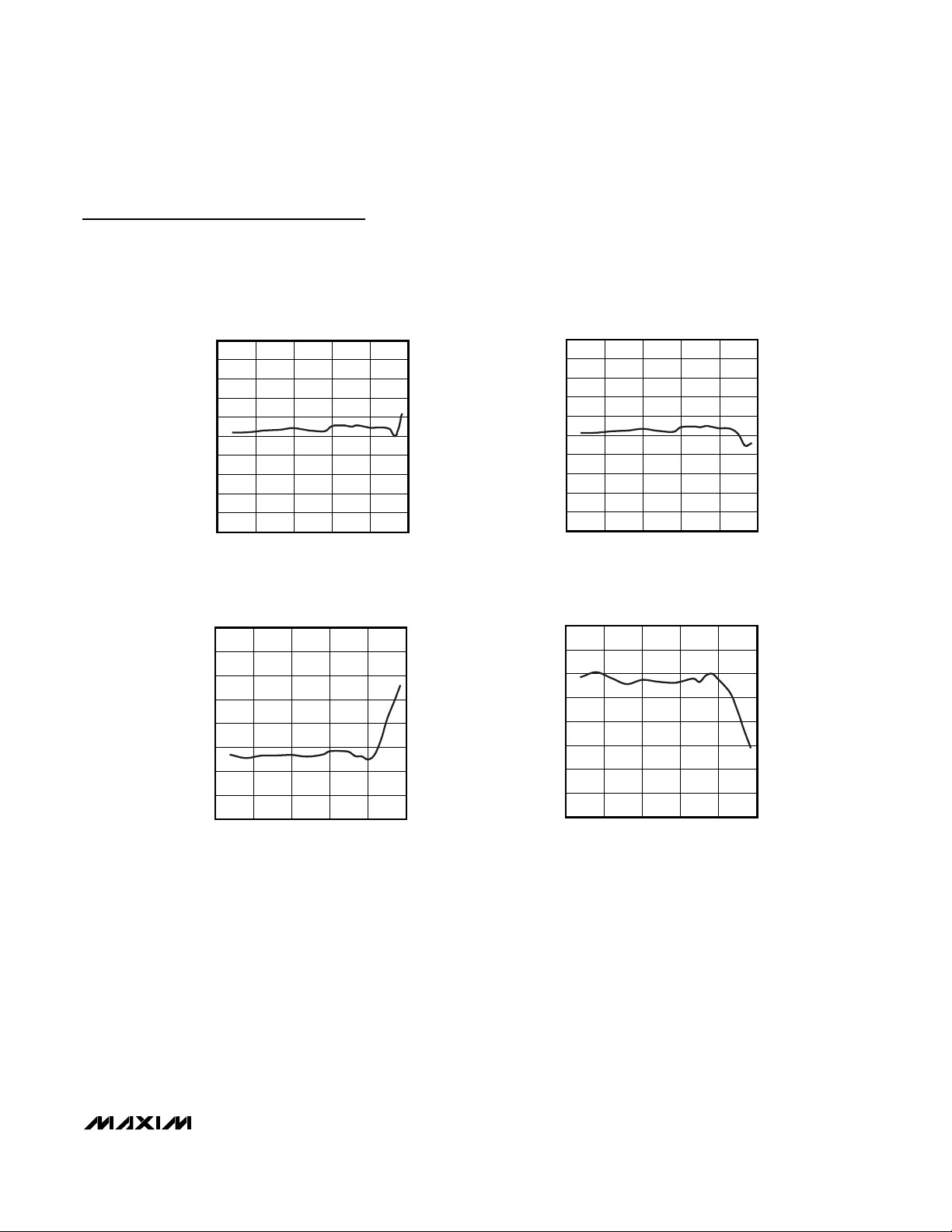
Typical Operating Characteristics
(AVDD= +5V, DVDD= +3V, AGND = DGND = 0, V
REF
= V
REFMS
= +2.5V (external reference), C
REF
= C
REFMS
= 0.1µF, C
REF+
=
C
REF-
= 0.1µF, C
REF+-to-REF-
= 2.2µF || 0.1µF, C
COM
= 2.2µF || 0.1µF, C
MSV
= 2.2µF || 0.1µF (unipolar devices), MSV = AGND (bipolar
devices), f
CLK
= 16.67MHz 50% duty cycle, INTCLK/EXTCLK = AGND (external clock), fIN= 500kHz, AIN= -0.4dBFS. TA= +25°C,
unless otherwise noted.) (Figures 3 and 4)
MAX1304–MAX1306/MAX1308–MAX1310/MAX1312–MAX1314
8-/4-/2-Channel, 12-Bit, Simultaneous-Sampling ADCs
with ±10V, ±5V, and 0 to +5V Analog Input Ranges
_______________________________________________________________________________________ 7
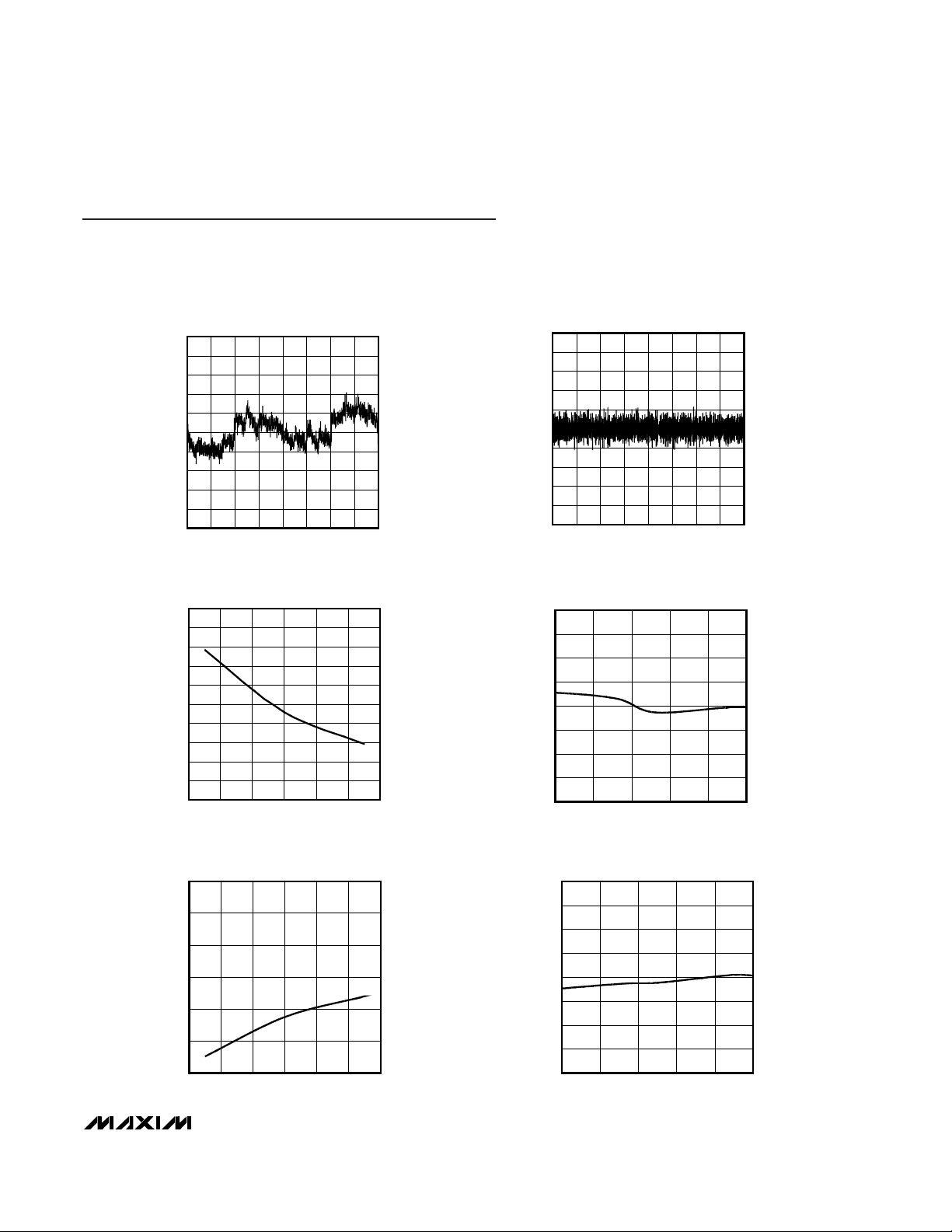
INTEGRAL NONLINEARITY
vs. DIGITAL OUTPUT CODE
MAX1304 toc01
DIGITAL OUTPUT CODE
INL (LSB)
358430722048 25601024 1536512
-0.8
-0.6
-0.4
-0.2
0
0.2
0.4
0.6
0.8
1.0
-1.0
04096
DIFFERENTIAL NONLINEARITY
vs. DIGITAL OUTPUT CODE
MAX1304 toc02
DIGITAL OUTPUT CODE
DNL (LSB)
358430722048 25601024 1536512
-0.8
-0.6
-0.4
-0.2
0
0.2
0.4
0.6
0.8
1.0
-1.0
04096
MAX1304 toc03
AVDD (V)
OFFSET ERROR (LSB)
5.25.15.04.94.8
-0.8
-0.6
-0.4
-0.2
0
0.2
0.4
0.6
0.8
1.0
-1.0
4.7 5.3
OFFSET ERROR
vs. ANALOG SUPPLY VOLTAGE
OFFSET ERROR
vs. TEMPERATURE
MAX1304 toc04
TEMPERATURE (°C)
OFFSET ERROR (LSB)
6035-15 10
-12
-8
-4
0
4
8
12
16
-16
-40 85
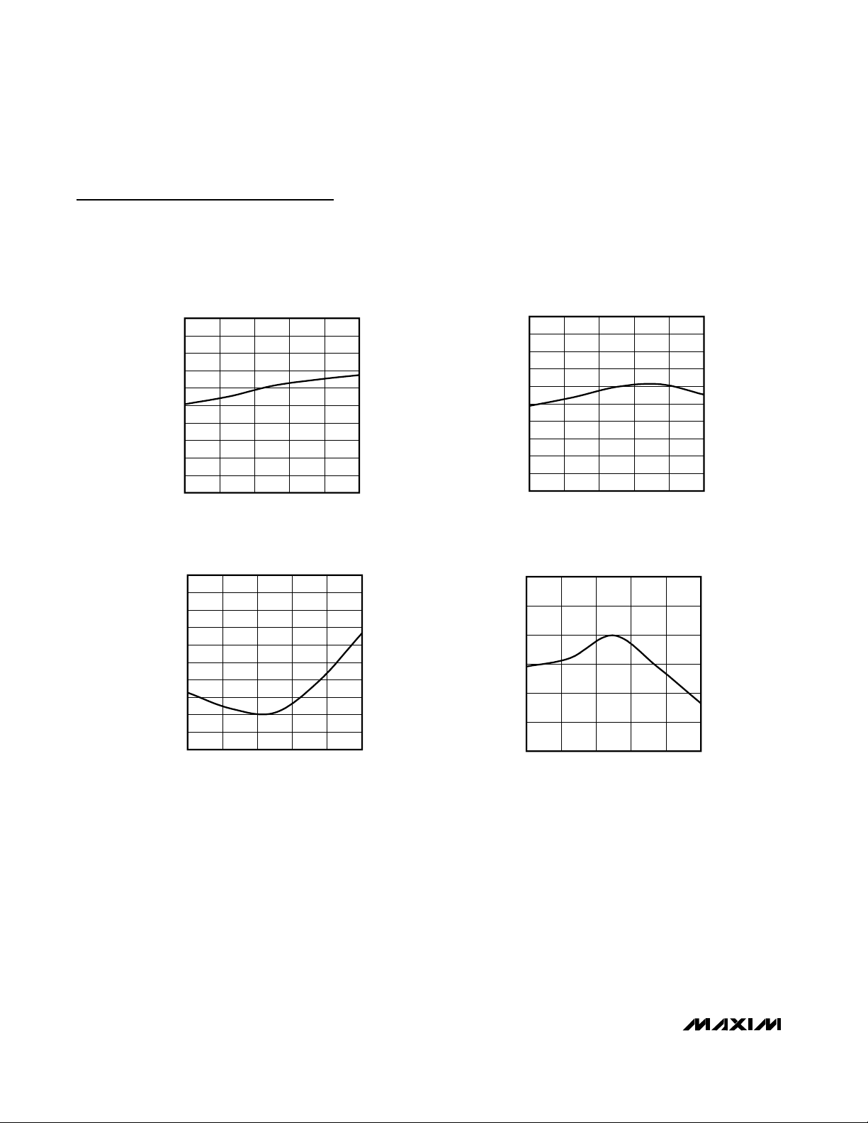
MAX1304 toc05
AVDD (V)
GAIN ERROR (LSB)
5.25.15.04.94.8
-4
-3
-2
-1
0
1
-5
4.7 5.3
GAIN ERROR
vs. ANALOG SUPPLY VOLTAGE
GAIN ERROR
vs. TEMPERATURE
MAX1304 toc06
TEMPERATURE (°C)
GAIN ERROR (LSB)
6035-15 10
-12
-8
-4
0
4
8
12
16
-16
-40 85
Page 8
Typical Operating Characteristics (continued)
(AVDD= +5V, DVDD= +3V, AGND = DGND = 0, V
REF
= V
REFMS
= +2.5V (external reference), C
REF
= C
REFMS
= 0.1µF, C
REF+
=
C
REF-
= 0.1µF, C
REF+-to-REF-
= 2.2µF || 0.1µF, C
COM
= 2.2µF || 0.1µF, C
MSV
= 2.2µF || 0.1µF (unipolar devices), MSV = AGND (bipolar
devices), f
CLK
= 16.67MHz 50% duty cycle, INTCLK/EXTCLK = AGND (external clock), fIN= 500kHz, AIN= -0.4dBFS. TA= +25°C,
unless otherwise noted.) (Figures 3 and 4)
MAX1304–MAX1306/MAX1308–MAX1310/MAX1312–MAX1314
8-/4-/2-Channel, 12-Bit, Simultaneous-Sampling ADCs
with ±10V, ±5V, and 0 to +5V Analog Input Ranges
8 _______________________________________________________________________________________
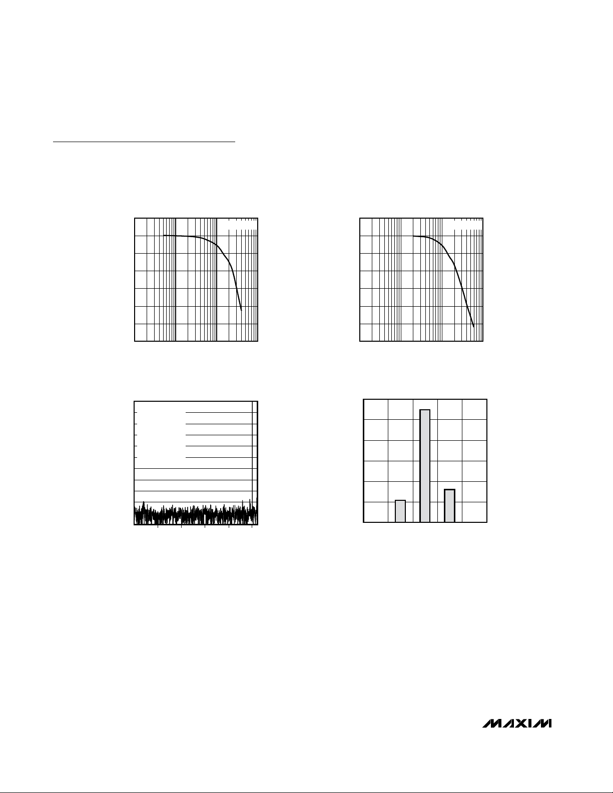
OUTPUT HISTOGRAM (DC INPUT)
MAX1304 toc10
DIGITAL OUTPUT CODE
COUNTS
2048204720462045
1000
2000
3000
4000
5000
6000
0
2044
00
1084
5497
1611
SMALL-SIGNAL BANDWIDTH
vs. ANALOG INPUT FREQUENCY
MAX1304 toc07
ANALOG INPUT FREQUENCY (MHz)
GAIN (dB)
101
-10
-8
-6
-4
-2
0
2
-12
0.1 100
AIN = -20dBFS
LARGE-SIGNAL BANDWIDTH
vs. ANALOG INPUT FREQUENCY
MAX1304 toc08
ANALOG INPUT FREQUENCY (MHz)
GAIN (dB)
101
-10
-8
-6
-4
-2
0
2
-12
0.1 100
AIN = -0.5dBFS
FFT PLOT
(2048-POINT DATA RECORD)
MAX1304 toc09
FREQUENCY (kHz)
AMPLITUDE (dBFS)
300
-100
-90
-80
-70
-60
-50
-40
-30
-20
-10
0
-110
0
100 200 400 500
fTH = 1.04167Msps
f
IN
= 500kHz
A
IN
= -0.05dBFS
SNR = 70.7dB
SINAD = 70.6dB
THD = -87.5dBc
SFDR = 87.1dBc
Page 9
Typical Operating Characteristics (continued)
(AVDD= +5V, DVDD= +3V, AGND = DGND = 0, V
REF
= V
REFMS
= +2.5V (external reference), C
REF
= C
REFMS
= 0.1µF, C
REF+
=
C
REF-
= 0.1µF, C
REF+-to-REF-
= 2.2µF || 0.1µF, C
COM
= 2.2µF || 0.1µF, C
MSV
= 2.2µF || 0.1µF (unipolar devices), MSV = AGND (bipolar
devices), f
CLK
= 16.67MHz 50% duty cycle, INTCLK/EXTCLK = AGND (external clock), fIN= 500kHz, AIN= -0.4dBFS. TA= +25°C,
unless otherwise noted.) (Figures 3 and 4)
MAX1304–MAX1306/MAX1308–MAX1310/MAX1312–MAX1314
8-/4-/2-Channel, 12-Bit, Simultaneous-Sampling ADCs
with ±10V, ±5V, and 0 to +5V Analog Input Ranges
_______________________________________________________________________________________ 9
-100
-95
-90
-85
-80
-75
-70
-65
-60
05101520 25
TOTAL HARMONIC DISTORTION
vs. CLOCK FREQUENCY
MAX1304 toc13
f
CLK
(MHz)
THD (dBc)
60
65
70
75
80
85
90
95
100
051015 20 25
SPURIOUS-FREE DYNAMIC RANGE
vs. CLOCK FREQUENCY
MAX1304 toc14
f
CLK
(MHz)
SFDR (dBc)
60
66
64
62
68
70
72
74
76
78
80
0105152025
SIGNAL-TO-NOISE RATIO
vs. CLOCK FREQUENCY
MAX1304 toc11
f
CLK
(MHz)
SNR (dB)
60
66
64
62
68
70
72
74
76
78
80
0105152025
SIGNAL-TO-NOISE PLUS DISTORTION
vs. CLOCK FREQUENCY
MAX1304 toc12
f
CLK
(MHz)
SINAD (dB)
Page 10
Typical Operating Characteristics (continued)
(AVDD= +5V, DVDD= +3V, AGND = DGND = 0, V
REF
= V
REFMS
= +2.5V (external reference), C
REF
= C
REFMS
= 0.1µF, C
REF+
=
C
REF-
= 0.1µF, C
REF+-to-REF-
= 2.2µF || 0.1µF, C
COM
= 2.2µF || 0.1µF, C
MSV
= 2.2µF || 0.1µF (unipolar devices), MSV = AGND (bipolar
devices), f
CLK
= 16.67MHz 50% duty cycle, INTCLK/EXTCLK = AGND (external clock), fIN= 500kHz, AIN= -0.4dBFS. TA= +25°C,
unless otherwise noted.) (Figures 3 and 4)
MAX1304–MAX1306/MAX1308–MAX1310/MAX1312–MAX1314
8-/4-/2-Channel, 12-Bit, Simultaneous-Sampling ADCs
with ±10V, ±5V, and 0 to +5V Analog Input Ranges
10 ______________________________________________________________________________________
SIGNAL-TO-NOISE RATIO
vs. REFERENCE VOLTAGE
MAX1304 toc15
V
REF
(V)
SNR (dB)
2.82.62.42.2
66
67
68
69
70
71
72
73
74
75
65
2.0 3.0
SIGNAL-TO-NOISE PLUS DISTORTION
vs. REFERENCE VOLTAGE
MAX1304 toc16
V
REF
(V)
SINAD (dB)
2.82.62.42.2
66
67
68
69
70
71
72
73
74
75
65
2.0 3.0
TOTAL HARMONIC DISTORTION
vs. REFERENCE VOLTAGE
MAX1304 toc17
V
REF
(V)
THD (dBc)
2.82.62.42.2
-88
-86
-84
-82
-80
-78
-76
-74
-72
-70
-90
2.0 3.0
SPURIOUS-FREE DYNAMIC RANGE
vs. REFERENCE VOLTAGE
MAX1304 toc18
V
REF
(V)
SFDR (dBc)
2.82.62.42.2
75
80
85
90
95
100
70
2.0 3.0
Page 11
Typical Operating Characteristics (continued)
(AVDD= +5V, DVDD= +3V, AGND = DGND = 0, V
REF
= V
REFMS
= +2.5V (external reference), C
REF
= C
REFMS
= 0.1µF, C
REF+
=
C
REF-
= 0.1µF, C
REF+-to-REF-
= 2.2µF || 0.1µF, C
COM
= 2.2µF || 0.1µF, C
MSV
= 2.2µF || 0.1µF (unipolar devices), MSV = AGND (bipolar
devices), f
CLK
= 16.67MHz 50% duty cycle, INTCLK/EXTCLK = AGND (external clock), fIN= 500kHz, AIN= -0.4dBFS. TA= +25°C,
unless otherwise noted.) (Figures 3 and 4)
MAX1304–MAX1306/MAX1308–MAX1310/MAX1312–MAX1314
8-/4-/2-Channel, 12-Bit, Simultaneous-Sampling ADCs
with ±10V, ±5V, and 0 to +5V Analog Input Ranges
______________________________________________________________________________________ 11
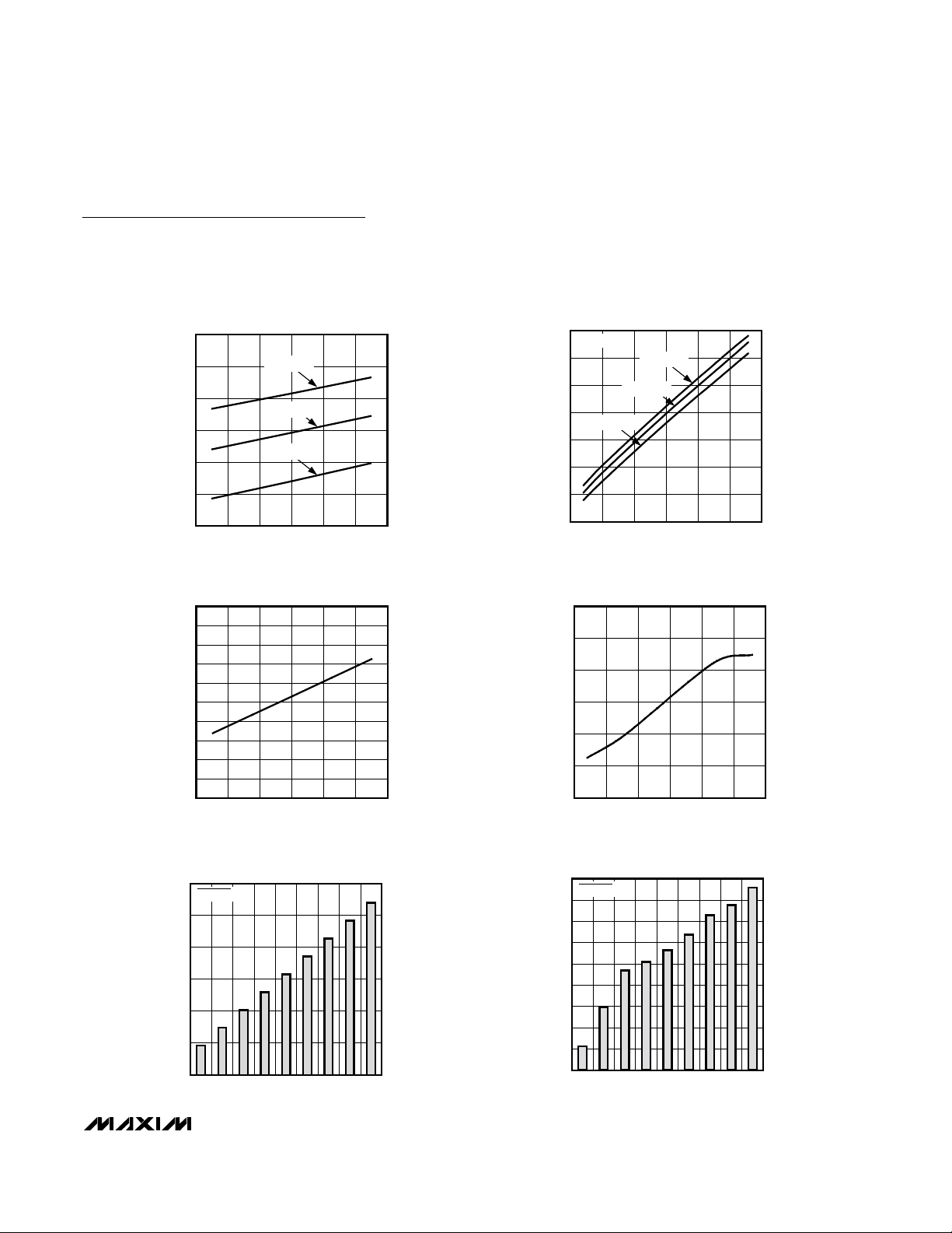
DIGITAL SUPPLY CURRENT
vs. DIGITAL SUPPLY VOLTAGE
MAX1304 toc20
DVDD (V)
I
DVDD
(mA)
5.04.54.03.53.0
0.8
1.0
1.2
1.4
1.6
1.8
2.0
0.6
2.5 5.5
TA = +85°C
TA = +25°C
TA = -40°C
C
LOAD
= 50pF
MAX1304 toc21
AVDD (V)
I
AVDD
(nA)
5.25.15.04.94.8
520
540
560
580
600
620
640
660
680
700
500
4.7 5.3
ANALOG SHUTDOWN CURRENT
vs. ANALOG SUPPLY VOLTAGE
DIGITAL SHUTDOWN CURRENT
vs. DIGITAL SUPPLY VOLTAGE
MAX1304 toc22
DVDD (V)
I
DVDD
(nA)
5.04.54.03.53.0
12
14
16
18
20
22
10
2.5 5.5
ANALOG SUPPLY CURRENT
vs. NUMBER OF CHANNELS SELECTED
MAX1304 toc23
NUMBER OF CHANNELS SELECTED
I
AVDD
(mA)
87654321
40
35
45
50
55
60
30
0
CHSHDN = 0
ANALOG SUPPLY CURRENT
vs. ANALOG SUPPLY VOLTAGE
MAX1304 toc19
AVDD (V)
I
AVDD
(mA)
5.25.15.04.94.8
52
53
54
55
56
57
51
4.7 5.3
TA = +85°C
TA = +25°C
TA = -40°C
DIGITAL SUPPLY CURRENT
vs. NUMBER OF CHANNELS SELECTED
MAX1304 toc24
NUMBER OF CHANNELS SELECTED
I
DVDD
(mA)
87654321
0.8
0.7
0.6
0.5
0.4
0.3
0.2
0.9
1.0
0.1
0
CHSHDN = 0
Page 12

Typical Operating Characteristics (continued)
(AVDD= +5V, DVDD= +3V, AGND = DGND = 0, V
REF
= V
REFMS
= +2.5V (external reference), C
REF
= C
REFMS
= 0.1µF, C
REF+
=
C
REF-
= 0.1µF, C
REF+-to-REF-
= 2.2µF || 0.1µF, C
COM
= 2.2µF || 0.1µF, C
MSV
= 2.2µF || 0.1µF (unipolar devices), MSV = AGND (bipolar
devices), f
CLK
= 16.67MHz 50% duty cycle, INTCLK/EXTCLK = AGND (external clock), fIN= 500kHz, AIN= -0.4dBFS. TA= +25°C,
unless otherwise noted.) (Figures 3 and 4)
MAX1304–MAX1306/MAX1308–MAX1310/MAX1312–MAX1314
8-/4-/2-Channel, 12-Bit, Simultaneous-Sampling ADCs
with ±10V, ±5V, and 0 to +5V Analog Input Ranges
12 ______________________________________________________________________________________
INTERNAL REFERENCE VOLTAGE
vs. ANALOG SUPPLY VOLTAGE
MAX1304 toc25
AVDD (V)
V
REF
(V)
5.25.14.8 4.9 5.0
2.4997
2.4998
2.4999
2.5000
2.5001
2.5002
2.5003
2.5004
2.4996
4.7 5.3
INTERNAL REFERENCE VOLTAGE
vs. TEMPERATURE
MAX1304 toc26
TEMPERATURE (°C)
V
REF
(V)
6035-15 10
2.497
2.498
2.499
2.500
2.501
2.502
2.503
2.504
2.496
-40 85
INTERNAL CLOCK CONVERSION TIME
vs. ANALOG SUPPLY VOLTAGE
MAX1304 toc27
AVDD (V)
TIME (ns)
5.25.15.04.94.8
100
200
300
400
500
600
700
800
900
0
4.7 5.3
t
NEXT
t
CONV
INTERNAL CLOCK CONVERSION TIME
vs. TEMPERATURE
MAX1304 toc28
TEMPERATURE (°C)
TIME (ns)
603510-15
180
200
780
800
820
160
-40 85
t
NEXT
t
CONV
MAX1304 toc29
V
CH_
(V)
I
CH_
(mA)
420-2-4
1.5
1.0
0.5
0
-0.5
-1.0
-1.5
2.0
-2.0
-6 6
ANALOG INPUT CHANNEL CURRENT
vs. ANALOG INPUT CHANNEL VOLTAGE
MAX1304/MAX1305/MAX1306
-3.0
-2.5
-1.0
-0.5
-1.5
-2.0
0
0.5
1.0
2.0
2.5
1.5
3.0
-20 -15 -10 -5 0 5 10 15 20
ANALOG INPUT CHANNEL CURRENT
vs. ANALOG INPUT CHANNEL VOLTAGE
MAX1304 toc30
V
CH_
(V)
I
CH_
(mA)
MAX1308/MAX1309/MAX1310
-2.0
-1.0
-1.5
0
-0.5
0.5
1.0
1.5
2.0
-20 -10 -5-15 0 5 101520
ANALOG INPUT CHANNEL CURRENT
vs. ANALOG INPUT CHANNEL VOLTAGE
MAX1304 toc31
V
CH_
(V)
I
CH_
(mA)
MAX1312/MAX1313/MAX1314
Page 13

MAX1304–MAX1306/MAX1308–MAX1310/MAX1312–MAX1314
8-/4-/2-Channel, 12-Bit, Simultaneous-Sampling ADCs
with ±10V, ±5V, and 0 to +5V Analog Input Ranges
______________________________________________________________________________________ 13
Pin Description
PIN
MAX1304
MAX1308
MAX1312
NAME
FUNCTION
1, 15, 17
Analog Power Input. AVDD is the power input for the analog section of the
converter. Apply +5V to AV
DD
. Connect all AVDD pins together. See the Layout,
Grounding, and Bypassing section for additional information.
2, 3, 14,
16, 23
2, 3, 14,
16, 23
2, 3, 14,
16, 23
Analog Ground. AGND is the power return for AV
DD
. Connect all AGND
pins together.
444CH0 Channel 0 Analog Input
555CH1 Channel 1 Analog Input
666MSV
Midscale Voltage Bypass. For the unipolar MAX1304/MAX1305/MAX1306,
connect a 2.2µF and a 0.1µF capacitor from MSV to AGND. For the bipolar
MAX1308/MAX1309/MAX1310/MAX1312/MAX1313/MAX1314, connect
MSV to AGND.
77—CH2 Channel 2 Analog Input
88—CH3 Channel 3 Analog Input
9——CH4 Channel 4 Analog Input
10 — — CH5 Channel 5 Analog Input
11 — — CH6 Channel 6 Analog Input
12 — — CH7 Channel 7 Analog Input
13 13 13
Clock-Mode Select Input. Connect INTCLK/EXTCLK to AV
DD
to select the
internal clock. Connect INTCLK/EXTCLK to AGND to use an external clock
connected to CLK.
18 18 18
Midscale Reference Bypass or Input. REFMS connects through a 5kΩ resistor to
the internal +2.5V bandgap reference buffer.
For the MAX1304/MAX1305/MAX1306 unipolar devices, V
REFMS
is the input to
the unity-gain buffer that drives MSV. MSV sets the midpoint of the input voltage
range. For internal reference operation, bypass REF
MS
with a ≥0.01µF
capacitor to AGND. For external reference operation, drive REF
MS
with an
external voltage from +2V to +3V.
For the MAX1308/MAX1309/MAX1310/MAX1312/MAX1313/MAX1314 bipolar
devices, connect REF
MS
to REF. For internal reference operation, bypass the
REF
MS
/REF node with a ≥0.01µF capacitor to AGND. For external reference
operation, drive the REFMS/REF node with an external voltage from +2V to +3V.
19 19 19 REF
ADC Reference Bypass or Input. REF connects through a 5kΩ resistor to the
internal +2.5V bandgap reference buffer.
For internal reference operation, bypass REF with a ≥0.01µF capacitor.
For external reference operation with the MAX1304/MAX1305/MAX1306
unipolar devices, drive REF with an external voltage from +2V to +3V.
For external reference operation with the MAX1308/MAX1309/MAX1310/
MAX1312/MAX1313/MAX1314 bipolar devices, connect REF
MS
to REF and
drive the REF
MS
/REF node with an external voltage from +2V to +3V.
MAX1305
MAX1309
MAX1313
1, 15, 17 1, 15, 17 AV
MAX1306
MAX1310
MAX1314
DD
AGND
INTCLK/
EXTCLK
REF
MS
Page 14

MAX1304–MAX1306/MAX1308–MAX1310/MAX1312–MAX1314
8-/4-/2-Channel, 12-Bit, Simultaneous-Sampling ADCs
with ±10V, ±5V, and 0 to +5V Analog Input Ranges
14 ______________________________________________________________________________________
Pin Description (continued)
PIN
FUNCTION
20 20 20
Positive Reference Bypass. Bypass REF+ with a 0.1µF capacitor to AGND. Also
bypass REF+ to REF- with a 2.2µF and a 0.1µF capacitor.
V
REF+
= V
COM
+ V
REF
/ 2.
21 21 21
Reference Common Bypass. Bypass COM to AGND with a 2.2µF and a 0.1µF
capacitor. V
COM
= 13 / 25 x AVDD.
22 22 22 REF-
Negative Reference Bypass. Bypass REF- with a 0.1µF capacitor to AGND.
Also bypass REF- to REF+ with a 2.2µF and a 0.1µF capacitor.
V
REF+
= V
COM
- V
REF
/ 2.
24, 39 24, 39 24, 39
Digital Ground. DGND is the power return for DV
DD
. Connect all DGND
pins together.
25, 38 25, 38 25, 38
Digital Power Input. DVDD powers the digital section of the converter, including
the parallel interface. Apply +2.7V to +5.25V to DV
DD
. Bypass DVDD to DGND
with a 0.1µF capacitor. Connect all DV
DD
pins together.
26 26 26 D0 D i g i tal I/O 0 of 12- Bi t P ar al l el D ata Bus. H i g h i m p ed ance w hen RD = 1 or CS = 1.
27 27 27 D1 D i g i tal I/O 1 of 12- Bi t P ar al l el D ata Bus. H i g h i m p ed ance w hen RD = 1 or CS = 1.
28 28 28 D2 D i g i tal I/O 2 of 12- Bi t P ar al l el D ata Bus. H i g h i m p ed ance w hen RD = 1 or CS = 1.
29 29 29 D3 D i g i tal I/O 3 of 12- Bi t P ar al l el D ata Bus. H i g h i m p ed ance w hen RD = 1 or CS = 1.
30 30 30 D4 D i g i tal I/O 4 of 12- Bi t P ar al l el D ata Bus. H i g h i m p ed ance w hen RD = 1 or CS = 1.
31 31 31 D5 D i g i tal I/O 5 of 12- Bi t P ar al l el D ata Bus. H i g h i m p ed ance w hen RD = 1 or CS = 1.
32 32 32 D6 D i g i tal I/O 6 of 12- Bi t P ar al l el D ata Bus. H i g h i m p ed ance w hen RD = 1 or CS = 1.
33 33 33 D7 D i g i tal I/O 7 of 12- Bi t P ar al l el D ata Bus. H i g h i m p ed ance w hen RD = 1 or CS = 1.
34 34 34 D8
Digital Output 8 of 12-Bit Parallel Data Bus. High impedance when RD = 1 or
CS = 1.
35 35 35 D9
Digital Output 9 of 12-Bit Parallel Data Bus. High impedance when RD = 1 or
CS = 1.
36 36 36 D10
Digital Output 10 of 12-Bit Parallel Data Bus. High impedance when RD = 1 or
CS = 1.
37 37 37 D11
Digital Output 11 of 12-Bit Parallel Data Bus. High impedance when RD = 1 or
CS = 1.
40 40 40 EOC
E nd - of- C onver si on Output. EOC goes low to i nd i cate the end of a conver si on. It
r etur ns hi g h on the next r i si ng C LK ed g e or the fal l i ng C ON V S T ed g e.
41 41 41
End-of-Last-Conversion Output. EOLC goes low to indicate the end of the
last conversion. It returns high when CONVST goes low for the next
conversion sequence.
42 42 42 RD Read Inp ut. P ul l i ng RD l ow i ni ti ates a r ead com m and of the p ar al l el d ata b us.
43 43 43 WR
Write Input. Pulling WR low initiates a write command for configuring the device
with D0–D7.
MAX1304
MAX1308
MAX1312
MAX1305
MAX1309
MAX1313
MAX1306
MAX1310
MAX1314
NAME
REF+
COM
DGND
DV
EOLC
DD
Page 15

MAX1304–MAX1306/MAX1308–MAX1310/MAX1312–MAX1314
8-/4-/2-Channel, 12-Bit, Simultaneous-Sampling ADCs
with ±10V, ±5V, and 0 to +5V Analog Input Ranges
______________________________________________________________________________________ 15
Detailed Description
The MAX1304–MAX1306/MAX1308–MAX1310/MAX1312–
MAX1314 are 12-bit ADCs. The devices offer 8, 4, or 2
independently selectable input channels, each with
dedicated T/H circuitry. Simultaneous sampling of all
active channels preserves relative phase information
making these devices ideal for motor control and power
monitoring. Three input ranges are available, 0 to +5V,
±5V and ±10V. The 0 to +5V devices provide ±6V faulttolerant inputs. The ±5V and ±10V devices provide
±16.5V fault-tolerant inputs. Two-channel conversion
results are available in 0.9µs. Conversion results from
all eight channels are available in 1.98µs. The 8-channel throughput is 456ksps per channel. Internal or
external reference and clock capability offer great flexibility, and ease of use. A write-only configuration register can mask out unused channels and a shutdown
feature reduces power. A 20MHz, 12-bit, parallel data
bus outputs the conversion results. Figure 2 shows the
functional diagram of these ADCs.
100pF
DEVICE PIN
V
DD
I
OL
= 1.6mA
I
OH
= 0.8mA
1.6V
Figure 1. Digital Load Test Circuit
Pin Description (continued)
PIN
MAX1304
MAX1308
MAX1312
NAME
FUNCTION
44 44 44 CS
Chip-Select Input. Pulling CS low activates the digital interface. Forcing CS high
places D0–D11 in high-impedance mode.
45 45 45
Conversion Start Input. Driving CONVST high initiates the conversion process.
The analog inputs are sampled on the rising edge of CONVST.
46 46 46 CLK
External Clock Input. For external clock operation, connect INTCLK/EXTCLK to
DGND and drive CLK with an external clock signal from 100kHz to 20MHz. For
internal clock operation, connect INTCLK/EXTCLK to DV
DD
and connect CLK to
DGND.
47 47 47
Shutdown Input. Driving SHDN high initiates device shutdown. Connect SHDN
to DGND for normal operation.
48 48 48
Active-Low Analog-Input Channel-Shutdown Input. Drive CHSHDN low to
power down analog inputs that are not selected for conversion in the
configuration register. Drive CHSHDN high to power up all analog input
channels regardless of whether they are selected for conversion in the
configuration register. See the Channel Shutdown (
CHSHDN
) section for more
information.
—
9, 10,
11, 12
7, 8, 9,
I.C. Internally connected. Connect I.C. to AGND.
MAX1305
MAX1309
MAX1313
MAX1306
MAX1310
MAX1314
10, 11, 12
C ON V S T
SHDN
CHSHDN
Page 16

MAX1304–MAX1306/MAX1308–MAX1310/MAX1312–MAX1314
8-/4-/2-Channel, 12-Bit, Simultaneous-Sampling ADCs
with ±10V, ±5V, and 0 to +5V Analog Input Ranges
16 ______________________________________________________________________________________
MAX1304–MAX1306
MAX1308–MAX1310
MAX1312–MAX1314
CONVST
D11
MSV
DGND
AV
DD
SHDN
INTCLK/EXTCLK
CLK
CH0
INTERFACE
AND
CONTROL
8 x 1
MUX
12-BIT
ADC
CH7
D0
DV
DD
AGND
CHSHDN
REF
MS
REF
REF+
COM
REF-
T/H
T/H
8 x 12
SRAM
OUTPUT
DRIVERS
5kΩ
5kΩ
CONFIGURATION
REGISTER
D7
D8
2.500V
*
*SWITCH CLOSED ON UNIPOLAR DEVICES, OPEN ON BIPOLAR DEVICES
WR
CS
RD
EOC
EOLC
Figure 2. Functional Diagram
Page 17

MAX1304–MAX1306/MAX1308–MAX1310/MAX1312–MAX1314
8-/4-/2-Channel, 12-Bit, Simultaneous-Sampling ADCs
with ±10V, ±5V, and 0 to +5V Analog Input Ranges
______________________________________________________________________________________ 17
MAX1308
MAX1312
CH0
CH7
CH6
CH5
CH4
CH3
CH2
CH1
D0
D1
D2
D3
D4
D5
D7
D8
D9
D10
D11
AV
DD
AGND
DV
DD
DGND
MSV
REF
MS
REF
REF+
COM
REF-
+5V
GND
+2.7V TO +5.25V
GND
CS
WR
BIPOLAR
ANALOG
INPUTS
PARALLEL
DIGITAL
OUTPUT
CONVST
RD
DIGITAL
INTERFACE
AND
CONTROL
4
5
7
8
9
10
11
12
2, 3, 14, 16, 23
21
22
20
19
18
6
17
48
47
46
25, 38
45
44
43
42
41
40
37
36
35
34
33
D6
32
31
30
29
28
27
26
24, 39
AV
DD
AV
DD
15
1
0.1µF
0.1µF
0.1µF
0.1µF
0.1µF
0.1µF
0.1µF
0.01µF
0.1µF
2.2µF
2.2µF
BIPOLAR
CONFIGURATION
CHSHDN
SHDN
CLK
EOLC
EOC
INTCLK/EXTCLK
13
Figure 3. Typical Bipolar Operating Circuit
Page 18

MAX1304–MAX1306/MAX1308–MAX1310/MAX1312–MAX1314
8-/4-/2-Channel, 12-Bit, Simultaneous-Sampling ADCs
with ±10V, ±5V, and 0 to +5V Analog Input Ranges
18 ______________________________________________________________________________________
MAX1304
CH0
CH7
CH6
CH5
CH4
CH3
CH2
CH1
D0
D1
D2
D3
D4
D5
D7
D8
D9
D10
D11
AV
DD
AGND
DV
DD
DGND
MSV
REF
MS
REF
REF+
COM
REF-
+5V
GND
+2.7V TO +5.25V
GND
CS
WR
UNIPOLAR
ANALOG
INPUTS
PARALLEL
DIGITAL
OUTPUT
CONVST
RD
DIGITAL
INTERFACE
AND
CONTROL
4
5
7
8
9
10
11
12
2, 3, 14, 16, 23
21
22
20
19
18
6
17
48
47
46
25, 38
45
44
43
42
41
40
37
36
35
34
33
D6
32
31
30
29
28
27
26
24, 39
AV
DD
AV
DD
15
1
0.1µF
0.1µF
0.1µF
0.1µF
0.1µF
0.1µF
0.1µF
0.01µF
0.1µF
2.2µF
2.2µF
UNIPOLAR
CONFIGURATION
0.1µF
2.2µF
CHSHDN
SHDN
CLK
EOLC
EOC
INTCLK/EXTCLK
13
0.01µF
Figure 4. Typical Unipolar Operating Circuit
Page 19

MAX1304–MAX1306/MAX1308–MAX1310/MAX1312–MAX1314
8-/4-/2-Channel, 12-Bit, Simultaneous-Sampling ADCs
with ±10V, ±5V, and 0 to +5V Analog Input Ranges
______________________________________________________________________________________ 19
Analog Inputs
Track and Hold (T/H)
To preserve phase information across the multichannel
MAX1304–MAX1306/MAX1308–MAX1310/MAX1312–
MAX1314, all input channels have dedicated T/H amplifiers. Figure 5 shows the equivalent analog input T/H
circuit for one channel.
The input T/H circuit is controlled by the CONVST input.
When CONVST is low, the T/H circuit tracks the analog
input. When CONVST is high the T/H circuit holds the
analog input. The rising edge of CONVST is the analog
input sampling instant. There is an aperture delay (tAD)
of 8ns and a 50ps
RMS
aperture jitter (tAJ). The aperture
delay of each dedicated T/H input is matched within
100ps of each other.
To settle the charge on C
SAMPLE
to 12-bit accuracy,
use a minimum acquisition time (t
ACQ
) of 100ns.
Therefore, CONVST must be low for at least 100ns.
Although longer acquisition times allow the analog input
to settle to its final value more accurately, the maximum
acquisition time must be limited to 1ms. Accuracy with
conversion times longer than 1ms cannot be guaranteed due to capacitor droop in the input circuitry.
Due to the analog input resistive divider formed by R1
and R2 in Figure 5, any significant analog input source
resistance (R
SOURCE
) results in gain error. Further-
more, R
SOURCE
causes distortion due to nonlinear
analog input currents. Limit R
SOURCE
to a maximum
of 100Ω.
Selecting an Input Buffer
To improve the input signal bandwidth under AC conditions, drive the input with a wideband buffer (>50MHz)
that can drive the ADC’s input capacitance (15pF) and
settle quickly. For example, the MAX4431 or the
MAX4265 can be used for the 0 to +5V unipolar devices,
or the MAX4350 can be used for ±5V bipolar inputs.
Most applications require an input buffer to achieve 12-bit
accuracy. Although slew rate and bandwidth are important, the most critical input buffer specification is settling
time. The simultaneous sampling of multiple channels
requires an acquisition time of 100ns. At the beginning of
the acquisition, the ADC internal sampling capacitor array
connects to the analog inputs, causing some disturbance. Ensure the amplifier is capable of settling to at
least 12-bit accuracy during this interval. Use a low-noise,
low-distortion, wideband amplifier that settles quickly and
is stable with the ADC’s 15pF input capacitance.
See the Maxim website at www.maxim-ic.com for application notes on how to choose the optimum buffer
amplifier for your ADC application.
Input Bandwidth
The input-tracking circuitry has a 20MHz small-signal
bandwidth, making it possible to digitize high-speed
transient events and measure periodic signals with
bandwidths exceeding the ADC’s sampling rate by
using undersampling techniques. To avoid high-frequency signals being aliased into the frequency band
of interest, anti-alias filtering is recommended.
Input Range and Protection
The MAX1304/MAX1305/MAX1306 provide a 0 to +5V
input voltage range with fault protection of ±6V. The
MAX1308/MAX1309/MAX1310 provide a ±5V input voltage range with fault protection of ±16.5V. The
MAX1312/MAX1313/MAX1314 provide a ±10V input
voltage range with fault protection of ±16.5V. Figure 5
shows the single-channel equivalent input circuit.
CH_
UNDERVOLTAGE
PROTECTION
CLAMP
OVERVOLTAGE
PROTECTION
CLAMP
R1
2.5pF
AV
DD
C
SAMPLE
C
HOLD
MAX1304–MAX1306
MAX1308–MAX1310
MAX1312–MAX1314
R1 | | R2 = 2kΩ
R2
V
BIAS
*R
SOURCE
ANALOG
SIGNAL
SOURCE
*MINIMIZE R
SOURCE
TO AVOID GAIN ERROR AND DISTORTION.
INPUT RANGE (V)PART
0 TO +5
MAX1304
MAX1305
MAX1306
MAX1308
MAX1309
MAX1310
MAX1312
MAX1313
MAX1314
±5
±10
R1 (kΩ)
3.33
6.67
13.33
R2 (kΩ) V
BIAS
(V)
5.00
2.86
2.35
0.90
2.50
2.06
Figure 5. Single-Channel, Equivalent Analog Input T/H Circuit
Page 20

MAX1304–MAX1306/MAX1308–MAX1310/MAX1312–MAX1314
8-/4-/2-Channel, 12-Bit, Simultaneous-Sampling ADCs
with ±10V, ±5V, and 0 to +5V Analog Input Ranges
20 ______________________________________________________________________________________
Data Throughput
The data throughput (fTH) of the MAX1304–MAX1306/
MAX1308–MAX1310/MAX1312–MAX1314 is a function
of the clock speed (f
CLK
). In internal clock mode, f
CLK
=
15MHz (typ). In external clock mode, 100kHz ≤ f
CLK
≤
20MHz. When reading during conversion (Figures 7 and
8), calculate fTHas follows:
where N is the number of active channels and t
QUIET
is
the period of bus inactivity before the rising edge of
CONVST. See the Starting a Conversion section for
more information.
Table 1 uses the above equation and shows the total
throughput as a function of the number of channels
selected for conversion.
Clock Modes
The MAX1304–MAX1306/MAX1308–MAX1310/MAX1312–
MAX1314 provide a 15MHz internal conversion clock.
Alternatively, an external clock can be used.
Internal Clock
Internal clock mode frees the microprocessor from the
burden of running the ADC conversion clock. For internal clock operation, connect INTCLK/EXTCLK to AV
DD
and connect CLK to DGND. Note that INTCLK/EXTCLK
is referenced to AVDD, not DVDD.
External Clock
For external clock operation, connect INTCLK/EXTCLK
to AGND and connect an external clock source to CLK.
Note that INTCLK/EXTCLK is referenced to AVDD, not
DVDD. The external clock frequency can be up to
20MHz. Linearity is not guaranteed with clock frequencies below 100kHz due to droop in the T/H circuits.
f
tt
xN
f
TH
ACQ QUIET
CLK
=
++
+ − +
1
12 3 1 1()
Table 1. Throughput vs. Channels Sampled: f
CLK
= 15MHz, t
ACQ
= 100ns, t
QUIET
= 50ns
CHANNELS
SAMPLED
(N)
CLOCK CYCLES
UNTIL
CLOCK CYCLE
FOR READING
TOTAL
TIME (ns)
TOTAL
THROUGHPUT
(ksps)
THROUGHPUT
PER CHANNEL
(fTH)
112 1800 983 983
21511000 1643 821
31811200 2117 705
42111400 2474 618
52411600 2752 550
62711800 2975 495
73012000 3157 451
83312200 3310 413
LAST RESULT
LAST CONVERSION
CONVERSION
Page 21

MAX1304–MAX1306/MAX1308–MAX1310/MAX1312–MAX1314
8-/4-/2-Channel, 12-Bit, Simultaneous-Sampling ADCs
with ±10V, ±5V, and 0 to +5V Analog Input Ranges
______________________________________________________________________________________ 21
Applications Information
Digital Interface
The bidirectional parallel digital interface allows for setting
the 8-bit configuration register (see the Configuration
Register section) and reading the 12-bit conversion
result. The interface includes the following control signals:
chip select (CS), read (RD), write (WR), end of conversion
(EOC), end of last conversion (EOLC), conversion start
(CONVST), shutdown (SHDN), channel shutdown
(CHSHDN), internal clock select (INTCLK/EXTCLK), and
external clock input (CLK). Figures 6, 7, 8, 9, Table 2, and
the Timing Characteristics show the operation of the inter-
face. D0–D7 are bidirectional, and D8–D11 are output
only. D0–D11 go high impedance when RD = 1 or CS = 1.
Configuration Register
Enable channels as active by writing to the configuration register through I/O lines D0–D7 (Table 2). The bits
in the configuration register map directly to the channels, with D0 controlling channel zero, and D7 controlling channel seven. Setting any bit high activates the
corresponding input channel, while resetting any bit
low deactivates the corresponding channel. On the
devices with less than eight channels, some of the bits
have no function (Table 2).
To write to the configuration register, pull CS and WR
low, load bits D0 through D7 onto the parallel bus, and
force WR high. The data are latched on the rising edge
of WR (Figure 6). Write to the configuration register at
any point during the conversion sequence. At powerup, write to the configuration register to select the
active channels before beginning a conversion.
However, the new configuration does not take effect
until the next CONVST falling edge. At power-up all
channels default active. Shutdown does not change the
configuration register. The configuration register may
be written to in shutdown. See the Channel Shutdown
(CHSHDN) section for information about using the configuration register for power saving.
Table 2. Configuration Register
BIT/CHANNEL
PART
NUMBER
STATE
D7/CH7
ON 1 1111111
MAX1304
MAX1308
MAX1312
OFF 0 0 0 0 0000
ON 1 111XXXX
MAX1305
MAX1309
MAX1313
OFF 0 000XXXX
ON 1 1 X X XXXX
MAX1306
MAX1310
MAX1314
OFF 0 0 X X XXXX
X = Don’t care (must be 1 or 0).
D0–D7
DATA-IN
RD
CONVST
CONFIGURATION
REGISTER UPDATES
CS
WR
t
CS
t
WRL
t
CTW
t
DTW
t
WTD
t
WTC
Figure 6. Write Timing
D0/CH0 D1/CH1 D2/CH2 D3/CH3 D4/CH4 D5/CH5 D6/CH6
Page 22

MAX1304–MAX1306/MAX1308–MAX1310/MAX1312–MAX1314
8-/4-/2-Channel, 12-Bit, Simultaneous-Sampling ADCs
with ±10V, ±5V, and 0 to +5V Analog Input Ranges
22 ______________________________________________________________________________________
Starting a Conversion
To start a conversion using internal clock mode, pull
CONVST low for the acquisition time (t
ACQ
). The T/H
acquires the signal while CONVST is low, and conversion begins on the rising edge of CONVST. The end-ofconversion signal (EOC) pulses low whenever a
conversion result becomes available for read. The endof-last-conversion signal (EOLC) goes low when the last
conversion result is available (Figure 7).
To start a conversion using external clock mode, pull
CONVST low for the acquisition time (t
ACQ
). The T/H
acquires the signal while CONVST is low. The rising
edge of CONVST is the sampling instant. Apply an
external clock to CLK to start the conversion. To avoid
T/H droop degrading the sampled analog input signals,
the first CLK pulse must occur within 10µs from the
rising edge of CONVST. Additionally, the external clock
frequency must be greater than 100kHz to avoid T/H
droop-degrading accuracy. The first conversion result
is available for read when EOC goes low on the rising
edge of the 13th clock cycle. Subsequent conversion
results are available after every third clock cycle thereafter (Figures 8 and 9).
In both internal and external clock modes, hold
CONVST high until the last conversion result is read. If
CONVST goes low in the middle of a conversion, the
current conversion is aborted and a new conversion is
initiated. Furthermore, there must be a period of bus
inactivity (t
QUIET
) for 50ns or longer before the falling
edge of CONVST for the specified ADC performance.
CONVST
CH0
TRACK
HOLD
D0–D11
SAMPLE
INSTANT
t
ACQ
t
EOC
t
ACC
t
CTR
t
RDH
t
RTC
t
RDL
t
REQ
TRACK
CH1
t
CONV
t
NEXT
EOC
t
CVEOLCD
t
QUIET
≥ 50ns
EOLC
CS*
RD
*CS CAN BE LOW AT ALL TIMES, LOW DURING THE RD CYCLES, OR THE SAME AS RD.
Figure 7. Read During Conversion—Channel 0 and Channel 1 Selected, Internal Clock
Page 23

MAX1304–MAX1306/MAX1308–MAX1310/MAX1312–MAX1314
8-/4-/2-Channel, 12-Bit, Simultaneous-Sampling ADCs
with ±10V, ±5V, and 0 to +5V Analog Input Ranges
______________________________________________________________________________________ 23
Reading a Conversion Result
Reading During a Conversion
Figures 7 and 8 show the interface signals to initiate a
read operation during a conversion cycle. These figures
show two channels selected for conversion. If more
channels are selected, the results are available successively at every EOC falling edge. CS can be low at all
times, low during the RD cycles, or the same as RD.
After initiating a conversion by bringing CONVST high,
wait for EOC to go low. In internal clock mode, EOC
goes low within 900ns. In external clock mode, EOC
goes low on the rising edge of the 13th CLK cycle. To
read the conversion result, drive CS and RD low to
latch data to the parallel digital output bus. Bring RD
high to release the digital bus. In internal clock mode,
the next EOC falling edge occurs within 225ns. In external clock mode, the next EOC falling edge occurs in
three CLK cycles. When the last result is available
EOLC goes low.
Reading After Conversion
Figure 9 shows the interface signals for a read operation
after a conversion with all eight channels enabled. At
the falling of EOLC, driving CS and RD low places the
first conversion result onto the parallel bus. Successive
low pulses of RD place the successive conversion
results onto the bus. When the last conversion results in
the sequence are read, additional read pulses wrap the
pointer back to the first converted result.
CONVST
CLK
CH3
TRACK
HOLD
D0–D11
SAMPLE
INSTANT
t
ACQ
t
CNTC
t
CTR
t
RDH
t
RTC
t
ACC
t
RDL
t
REQ
TRACK
CH7
EOC
RD
1231213 14 15 16 17 18 19 1
t
CLK
t
EOCD
t
CONV
t
NEXT
t
EOC
t
EOCD
t
CLKH
t
EOLCD
t
CVEOLCD
t
QUIET
≥ 50ns
t
CLKL
EOLC
CS*
*CS CAN BE LOW AT ALL TIMES, LOW DURING THE RD CYCLES, OR THE SAME AS RD.
Figure 8. Read During Conversion—Channel 3 and Channel 7 Selected, External Clock
Page 24

MAX1304–MAX1306/MAX1308–MAX1310/MAX1312–MAX1314
8-/4-/2-Channel, 12-Bit, Simultaneous-Sampling ADCs
with ±10V, ±5V, and 0 to +5V Analog Input Ranges
24 ______________________________________________________________________________________
Power-Up Reset
At power-up, all channels are selected for conversion
(see the Configuration Register section). After applying
power, allow the 1ms wake-up time to elapse and then
initiate a dummy conversion and discard the results.
After the dummy conversion is complete, accurate conversions can be obtained.
Power-Saving Modes
Shutdown Mode
During shutdown the internal reference and analog
circuits in the device shutdown and the analog supply
current drops to 0.6µA (typ). Select shutdown mode
using the SHDN input. Set SHDN high to enter shutdown mode. SHDN takes precedence over CHSHDN.
Entering and exiting shutdown mode does not change
the configuration byte. However, a new configuration
byte can be written while in shutdown mode by following the standard write procedure shown in Figure 6.
EOC and EOLC are high when the MAX1304–MAX1306/
MAX1308–MAX1310/MAX1312–MAX1314 are shut down.
The state of the digital outputs D0–D11 is independent
of the state of SHDN. If CS and RD are low, the digital
outputs D0–D11 are active regardless of SHDN. The
digital outputs only go high impedance when CS or RD
is high. When the digital outputs are powered down, the
digital supply current drops to 20nA.
Exiting shutdown (falling edge of SHDN) starts a conversion in the same way as the rising edge of CONVST.
After coming out of shutdown, initiate a dummy conversion and discard the results. After the dummy conversion, allow the 1ms wake-up time to expire before
initiating the first accurate conversion.
Channel Shutdown (CCHHSSHHDDNN)
The channel-shutdown feature allows analog input
channels to be powered down when they are not
selected for conversion. Powering down channels that
are not selected for conversion reduces the analog
supply current by 2.9mA per channel. To power down
channels that are not selected for conversion, pull
CHSHDN low. See the Configuration Register section
for information on selecting and deselecting channels
for conversion.
The drawback of powering down analog inputs that are
not selected for conversion is that it takes time to power
them up. Figure 10 shows how a dummy conversion is
used to power up an analog input in external clock
mode. After selecting a new channel in the configuration register, initiate a dummy conversion and discard
the results. After the dummy conversion, allow the 1ms
wake-up time (t
WAKE
) to expire before initiating the first
accurate conversion.
D0–D11
CONVST
t
CTR
t
ACC
t
REQ
t
RDL
t
RDH
t
RTC
t
CVEOLCD
t
EOC
t
QUIET1
= 50ns
CH0 CH1 CH2 CH3 CH4 CH5 CH6 CH7
ONLY LAST PULSE SHOWN
EOC
RD
CS*
EOLC
* CS CAN BE LOW AT ALL TIMES, LOW DURING THE RD CYCLES, OR THE SAME AS RD.
Figure 9. Read After Conversion—Eight Channels Selected, External Clock
Page 25

MAX1304–MAX1306/MAX1308–MAX1310/MAX1312–MAX1314
8-/4-/2-Channel, 12-Bit, Simultaneous-Sampling ADCs
with ±10V, ±5V, and 0 to +5V Analog Input Ranges
______________________________________________________________________________________ 25
CONVST
CLK
EOC
CS*
EOLC
t
ACQ
t
ACQ
DUMMY
CONVERSION
START
CONFIGURATION REGISTER
POWERS UP ONE OR
MORE CHANNELS
FIRST ACCURATE
CONVERSION
START
CONFIGURATION
REGISTER
UPDATES
12345 1213 1
t
WAKE
≥ 1ms
WR
D0–D7
*CS CAN BE LOW AT ALL TIMES, LOW DURING THE RD CYCLES, OR THE SAME AS RD.
DATA
IN
Figure 10. Powering Up an Analog Input Channel with a Dummy Conversion and Wake-Up Time (
CHSHDN
= 0, External-Clock
Mode, One Channel Selected)
CONVST
CLK
EOC
CS*
EOLC
t
ACQ
t
ACQ
FIRST ACCURATE
CONVERSION START
CONFIGURATION REGISTER
POWERS UP ONE OR
MORE CHANNELS
SECOND ACCURATE
CONVERSION START
CONFIGURATION
REGISTER
UPDATES
12345 1213 1
WR
D0–D7
*CS CAN BE LOW AT ALL TIMES, LOW DURING THE RD CYCLES, OR THE SAME AS RD.
DATA
IN
Figure 11. Powering Up an Analog Input Channel Directly (
CHSHDN
= 1, External-Clock Mode, One Channel Selected)
Page 26

MAX1304–MAX1306/MAX1308–MAX1310/MAX1312–MAX1314
8-/4-/2-Channel, 12-Bit, Simultaneous-Sampling ADCs
with ±10V, ±5V, and 0 to +5V Analog Input Ranges
26 ______________________________________________________________________________________
To avoid the timing requirements associated with powering up an analog channel, force CHSHDN high. With
CHSHDN high, each analog input is powered up
regardless of whether it is selected for conversion in
the configuration register. Note that shutdown mode
takes precedence over the CHSHDN mode.
Reference
Internal Reference
The internal reference circuits provide for analog input
voltages of 0 to +5V for the unipolar MAX1304/
MAX1305/MAX1306, ±5V for the bipolar MAX1308/
MAX1309/MAX1310 or ±10V for the bipolar MAX1312/
MAX1313/MAX1314. Install external capacitors for reference stability, as indicated in Table 3 and shown in
Figures 3 and 4.
As illustrated in Figure 2, the internal reference voltage
is 2.5V (V
REF
). This 2.5V is internally buffered to create
the voltages at REF+ and REF-. Table 4 shows the voltages at COM, REF+, and REF-.
External Reference
External reference operation is achieved by overriding
the internal reference voltage. Override the internal ref-
erence voltage by driving REF with a +2.0V to +3.0V
external reference. As shown in Figure 2, the REF input
impedance is 5kΩ. For more information about using
external references see the Transfer Functions section.
Midscale Voltage (MSV)
The voltage at MSV (V
MSV
) sets the midpoint of the ADC
transfer functions. For the 0 to +5V input range (unipolar
devices), the midpoint of the transfer function is +2.5V.
For the ±5V and ±10V input range devices, the midpoint
of the transfer function is zero.
As shown in Figure 2, there is a unity-gain buffer
between REFMSand MSV in the unipolar MAX1304/
MAX1305/MAX1306. This midscale buffer sets the midpoint of the unipolar transfer functions to either the internal +2.5V reference or an externally applied voltage at
REFMS. V
MSV
follows V
REFMS
within ±3mV.
The midscale buffer is not active for the bipolar
devices. For these devices, MSV must be connected to
AGND or externally driven. REF
MS
must be bypassed
with a 0.01µF capacitor to AGND.
See the Transfer Functions section for more information
about MSV.
Table 3. Reference Bypass Capacitors
INPUT VOLTAGE RANGE
LOCATION
UNIPOLAR (µF) BIPOLAR (µF)
MSV Bypass Capacitor to AGND 2.2 || 0.1 N/A
REFMS Bypass Capacitor to AGND 0.01 0.01
REF Bypass Capacitor to AGND 0.01 0.01
REF+ Bypass Capacitor to AGND 0.1 0.1
REF+ to REF- Capacitor 2.2 || 0.1 2.2 || 0.1
REF- Bypass Capacitor to AGND 0.1 0.1
COM Bypass Capacitor to AGND 2.2 || 0.1 2.2 || 0.1
Table 4. Reference Voltages
PARAMETER
EQUATION
CALCULATED VALUE (V)
V
REF
= 2.000V,
AV
DD
= 5.0V
CALCULATED VALUE (V)
V
REF
= 2.500V,
AV
DD
= 5.0V
CALCULATED VALUE (V)
V
REF
= 3.000V,
AV
DD
= 5.0V
V
COM
2.600 2.600 2.600
V
REF+
3.600 3.850 4.100
V
REF-
1.600 1.350 1.100
V
REF+
- V
REF-
V
REF-
- V
REF+
= V
REF
2.000 2.500 3.000
N/A = Not applicable. Connect MSV directly to AGND.
(
V
= 13 / 25 x AV
COM
V
= V
REF+
V
REF-
= V
COM
COM
+ V
- V
DD
/ 2
REF
/ 2
REF
)
(
)
()
Page 27

MAX1304–MAX1306/MAX1308–MAX1310/MAX1312–MAX1314
8-/4-/2-Channel, 12-Bit, Simultaneous-Sampling ADCs
with ±10V, ±5V, and 0 to +5V Analog Input Ranges
______________________________________________________________________________________ 27
Transfer Functions
Unipolar 0 to +5V Devices
Table 5 and Figure 12 show the offset binary transfer
function for the MAX1304/MAX1305/MAX1306 with a 0
to +5V input range. The full-scale input range (FSR) is
two times the voltage at REF. The internal +2.5V reference gives a +5V FSR, while an external +2V to +3V
reference allows an FSR of +4V to +6V, respectively.
Calculate the LSB size using:
which equals 1.22mV when using a 2.5V reference.
The input range is centered about V
MSV
, internally set
to +2.5V. For a custom midscale voltage, drive REF
MS
with an external voltage source and MSV will follow
REFMS. Noise present on MSV or REFMSdirectly couples into the ADC result. Use a precision, low-drift voltage reference with adequate bypassing to prevent MSV
from degrading ADC performance. For maximum FSR,
do not violate the absolute maximum voltage ratings of
the analog inputs when choosing MSV.
Determine the input voltage as a function of V
REF
,
V
MSV
, and the output code in decimal using:
V
CH_
= LSB x CODE10+ V
MSV
- 2.500V
1
2
2
12
LSB
xV
REF
=
Table 5. 0 to 5V Unipolar Code Table
BINARY
DIGITAL
OUTPUT CODE
DECIMAL
EQUIVALENT
DIGITAL OUTPUT
CODE
(CODE
10
)
INPUT VOLTAGE
(V)
V
REF
= +2.5V
V
REFMS
= +2.5V
1111 1111 1111
= 0xFFF
4095
+4.9994 ± 0.5 LSB
1111 1111 1110
= 0xFFE
4094
+4.9982 ± 0.5 LSB
1000 0000 0001
= 0x801
2049
+2.5018 ± 0.5 LSB
1000 0000 0000
= 0x800
2048
+2.5006 ± 0.5 LSB
0111 1111 1111
= 0x7FF
2047
+2.4994 ± 0.5 LSB
0000 0000 0001
= 0x001
1
+0.0018 ± 0.5 LSB
0000 0000 0000
= 0x000
0
+0.0006 ± 0.5 LSB
)
Figure 12. 0 to +5V Unipolar Transfer Function
(
0xFFF
0xFFE
0xFFD
0xFFC
2 x V
REF
0x801
0x800
0x7FF
BINARY OUTPUT CODE
0x0003
0x0002
0x0001
0x0000
021
2046 2048
3
INPUT VOLTAGE (LSBs)
2050
(MSV)
1 LSB =
2 x V
REF
12
2
40954093
Page 28

MAX1304–MAX1306/MAX1308–MAX1310/MAX1312–MAX1314
8-/4-/2-Channel, 12-Bit, Simultaneous-Sampling ADCs
with ±10V, ±5V, and 0 to +5V Analog Input Ranges
28 ______________________________________________________________________________________
Bipolar ±5V Devices
Table 6 and Figure 13 show the two’s complement transfer function for the ±5V input range MAX1308/MAX1309/
MAX1310. The FSR is four times the voltage at REF. The
internal +2.5V reference gives a +10V FSR, while an
external +2V to +3V reference allows an FSR of +8V to
+12V respectively. Calculate the LSB size using:
which equals 2.44mV when using a 2.5V reference.
The input range is centered about V
MSV
. Normally,
MSV = AGND, and the input is symmetrical about zero.
For a custom midscale voltage, drive MSV with an
external voltage source. Noise present on MSV directly
couples into the ADC result. Use a precision, low-drift
voltage reference with adequate bypassing to prevent
MSV from degrading ADC performance. For maximum
FSR, do not violate the absolute maximum voltage ratings of the analog inputs when choosing MSV.
Determine the input voltage as a function of V
REF
,
V
MSV
, and the output code in decimal using:
V
CH_
= LSB x CODE10+ V
MSV
1
4
2
12
LSB
xV
REF
=
Table 6. ±5V Bipolar Code Table
TWO’s
COMPLEMENT
DIGITAL OUTPUT
CODE
DECIMAL
EQUIVALENT
DIGITAL OUTPUT
CODE
(CODE
10
)
INPUT VOLTAGE
(V)
V
REF
= +2.5V
V
MSV
= 0
0111 1111 1111 =
0x7FF
+2047
+4.9988 ± 0.5 LSB
0111 1111 1110 =
0x7FE
+2046
+4.9963 ± 0.5 LSB
0000 0000 0001 =
0x001
+1
+0.0037 ± 0.5 LSB
0000 0000 0000 =
0x000
0
+0.0012 ± 0.5 LSB
1111 1111 1111 =
0xFFF
-1
-0.0012 ± 0.5 LSB
1000 0000 0001 =
0x801
-2047
-4.9963 ± 0.5 LSB
1000 0000 0000 =
0x800
-2048
-4.9988 ± 0.5 LSB
)
Figure 13. ±5V Bipolar Transfer Function
(
0x7FF
0x7FE
0x7FD
0x7FC
0x001
0x000
0xFFF
4 x V
REF
0x803
TWO'S COMPLEMENT BINARY OUTPUT CODE
0x802
0x801
0x800
-2048 -2046 +2047+2045
INPUT VOLTAGE (V
-1 0 +1
(MSV)
CH_
- V
MSV
1 LSB =
IN LSBs)
4 x V
REF
12
2
Page 29

MAX1304–MAX1306/MAX1308–MAX1310/MAX1312–MAX1314
8-/4-/2-Channel, 12-Bit, Simultaneous-Sampling ADCs
with ±10V, ±5V, and 0 to +5V Analog Input Ranges
______________________________________________________________________________________ 29
Bipolar ±10V Devices
Table 7 and Figure 14 show the two’s complement transfer function for the ±10V input range MAX1312/
MAX1313/MAX1314. The FSR is eight times the voltage at
REF. The internal +2.5V reference gives a +20V FSR,
while an external +2V to +3V reference allows an FSR of
+16V to +24V, respectively. Calculate the LSB size using:
which equals 4.88mV with a +2.5V internal reference.
The input range is centered about V
MSV
. Normally,
MSV = AGND, and the input is symmetrical about zero.
For a custom midscale voltage, drive MSV with an
external voltage source. Noise present on MSV directly
couples into the ADC result. Use a precision, low-drift
voltage reference with adequate bypassing to prevent
MSV from degrading ADC performance. For maximum
FSR, do not violate the absolute maximum voltage ratings of the analog inputs when choosing MSV.
Determine the input voltage as a function of V
REF
,
V
MSV
, and the output code in decimal using:
V
CH_
= LSB x CODE10+ V
MSV
1
8
2
12
LSB
xV
REF
=
Table 7. ±10V Bipolar Code Table
TWO’s
COMPLEMENT
DIGITAL OUTPUT
CODE
DECIMAL
EQUIVALENT
DIGITAL OUTPUT
CODE
(CODE
10
)
INPUT VOLTAGE
(V)
V
REF
= +2.5V
V
MSV
= 0
0111 1111 1111 =
0x7FF
+2047
+9.9976 ± 0.5 LSB
0111 1111 1110 =
0x7FE
+2046
+9.9927 ± 0.5 LSB
0000 0000 0001 =
0x001
+1
+0.0073 ± 0.5 LSB
0000 0000 0000 =
0x000
0
0.0024 ± 0.5 LSB
1111 1111 1111 =
0xFFF
-1
-0.0024 ± 0.5 LSB
1000 0000 0001 =
0x801
-2047
-9.9927 ± 0.5 LSB
1000 0000 0000 =
0x800
-2048
-9.9976 ± 0.5 LSB
)
Figure 14. ±10V Bipolar Transfer Function
(
0x7FF
0x7FE
0x7FD
0x7FC
0x001
0x000
0xFFF
8 x V
REF
0x803
TWO'S COMPLEMENT BINARY OUTPUT CODE
0x802
0x801
0x800
-2048 -2046 +2047+2045
INPUT VOLTAGE (V
-1 0 +1
(MSV)
CH_
- V
MSV
1 LSB =
IN LSBs)
8 x V
REF
12
2
Page 30

MAX1304–MAX1306/MAX1308–MAX1310/MAX1312–MAX1314
8-/4-/2-Channel, 12-Bit, Simultaneous-Sampling ADCs
with ±10V, ±5V, and 0 to +5V Analog Input Ranges
30 ______________________________________________________________________________________
3-Phase Motor Controller
The MAX1304–MAX1306/MAX1308–MAX1310/MAX1312–
MAX1314 are ideally suited for motor-control systems
(Figure 15). The devices’ simultaneously sampled
inputs eliminate the need for complicated DSP algo-
rithms that realign sequentially sampled data into a
simultaneous sample set. Additionally, the variety of
input voltage ranges allows for flexibility when choosing
current sensors and position encoders.
12-BIT
ADC
DSP
CURRENT
SENSOR
I
PHASE1
PHASE 1
PHASE 2
PHASE 3
3-PHASE ELECTRIC MOTOR
POSITION
ENCODER
I
PHASE3
I
PHASE2
IGBT CURRENT DRIVERS
T/H
MAX1308
Figure 15. 3-Phase Motor Control
Page 31

MAX1304–MAX1306/MAX1308–MAX1310/MAX1312–MAX1314
8-/4-/2-Channel, 12-Bit, Simultaneous-Sampling ADCs
with ±10V, ±5V, and 0 to +5V Analog Input Ranges
______________________________________________________________________________________ 31
3-Phase Power-Monitoring System
The 8-channel devices are well suited for use in
3-phase power monitoring (Figure 16). The simultane-
ously sampled eight channels eliminate the need for
complicated DSP algorithms that realign sequentially
sampled data into a simultaneous sample set.
12-BIT
ADC
MICROCONTROLLER
LOAD
I
P1
I
P2
I
P3
V
P2
PHASE 1
NEUTRAL
PHASE 2
PHASE 3
V
P1
V
NEUTRAL
V
P3
BUFFERS
AND INPUT
PROTECTION
I
Pn
T/H
CURRENT
TRANSFORMER
CURRENT
TRANSFORMER
CURRENT
TRANSFORMER
CURRENT
TRANSFORMER
POWER
GRID
MAX1312
LOAD
LOAD
Figure 16. 3-Phase Power Monitoring
Page 32

MAX1304–MAX1306/MAX1308–MAX1310/MAX1312–MAX1314
8-/4-/2-Channel, 12-Bit, Simultaneous-Sampling ADCs
with ±10V, ±5V, and 0 to +5V Analog Input Ranges
32 ______________________________________________________________________________________
Layout, Grounding, and Bypassing
For best performance use PC boards. Board layout must
ensure that digital and analog signal lines are separated
from each other. Do not run analog and digital lines parallel to one another (especially clock lines), and do not run
digital lines underneath the ADC package.
Figure 17 shows the recommended system ground connections. Establish an analog ground point at AGND and
a digital ground point at DGND. Connect all analog
grounds to the analog ground point. Connect all digital
grounds to the digital ground point. For lowest noise
operation, make the power-supply ground returns as low
impedance and as short as possible. Connect the analog
ground point to the digital ground point at one location.
High-frequency noise in the power supplies degrades
the ADC’s performance. Bypass the analog power
plane to the analog ground plane with a 2.2µF capacitor within one inch of the device. Bypass each AVDDto
AGND pair of pins with a 0.1µF capacitor as close to
the device as possible. AVDDto AGND pairs are pin 1
to pin 2, pin 14 to pin 15, and pin 16 to pin 17.
Likewise, bypass the digital power plane to the digital
ground plane with a 2.2µF capacitor within one inch of
the device. Bypass each DVDDto DGND pair of pins
with a 0.1µF capacitor as close to the device as possible. DVDDto DGND pairs are pin 24 to pin 25, and pin
38 to pin 39. If a supply is very noisy use a ferrite bead
as a lowpass filter as shown in Figure 17.
Definitions
Integral Nonlinearity (INL)
INL is the deviation of the values on an actual transfer
function from a straight line. For these devices, this
straight line is drawn between the endpoints of the
transfer function, once offset and gain errors have
been nullified.
Differential Nonlinearity (DNL)
DNL is the difference between an actual step width and
the ideal value of 1 LSB. For these devices, the DNL of
each digital output code is measured and the worstcase value is reported in the electrical characteristics
table. A DNL error specification of less than ±1 LSB
guarantees no missing codes and a monotonic
transfer function.
Offset Error
Offset error is a figure of merit that indicates how well
the actual transfer function matches the ideal transfer
function at a single point. Typically the point at which
offset error is specified is either at or near the zeroscale point of the transfer function or at or near the midscale point of the transfer function.
For the unipolar devices (MAX1304/MAX1305/
MAX1306), the ideal zero-scale transition from 0x000 to
0x001 occurs at 1 LSB above AGND (Figure 12, Table 5).
Unipolar offset error is the amount of deviation between
the measured zero-scale transition point and the ideal
zero-scale transition point.
For the bipolar devices (MAX1308/MAX1309/MAX1310/
MAX1312/MAX1313/MAX1314), the ideal midscale transition from 0xFFF to 0x000 occurs at MSV (Figures 14
and 13, Tables 7 and 6). The bipolar offset error is the
amount of deviation between the measured midscale
transition point and the ideal midscale transition point.
ANALOG SUPPLY
AV
DD AGND DV
DD
DATA
DGND
DIGITAL
CIRCUITRY
OPTIONAL
FERRITE
BEAD
+5V RETURN
DIGITAL
GROUND
POINT
DIGITAL SUPPLY
RETURN +3V TO +5V
DGND
DV
DD
MAX1304–MAX1306
MAX1308–MAX1310
MAX1312–MAX1314
ANALOG
GROUND
POINT
Figure 17. Power-Supply Grounding and Bypassing
Page 33

MAX1304–MAX1306/MAX1308–MAX1310/MAX1312–MAX1314
8-/4-/2-Channel, 12-Bit, Simultaneous-Sampling ADCs
with ±10V, ±5V, and 0 to +5V Analog Input Ranges
______________________________________________________________________________________ 33
Gain Error
Gain error is a figure of merit that indicates how well the
slope of the actual transfer function matches the slope
of the ideal transfer function. For the MAX1304–
MAX1306/MAX1308–MAX1310/MAX1312–MAX1314, the
gain error is the difference of the measured full-scale
and zero-scale transition points minus the difference of
the ideal full-scale and zero-scale transition points.
For the unipolar devices (MAX1304/MAX1305/
MAX1306), the full-scale transition point is from 0xFFE
to 0xFFF and the zero-scale transition point is from
0x000 to 0x001.
For the bipolar devices (MAX1308/MAX1309/MAX1310/
MAX1312/MAX1313/MAX1314), the full-scale transition
point is from 0x7FE to 0x7FF and the zero-scale transition point is from 0x800 to 0x801.
Signal-to-Noise Ratio (SNR)
For a waveform perfectly reconstructed from digital
samples, the theoretical maximum SNR is the ratio of
the full-scale analog input (RMS value) to the RMS
quantization error (residual error). The ideal, theoretical
minimum analog-to-digital noise is caused by quantization error only and results directly from the ADC’s resolution (N bits):
SNR
dB[max]
= 6.02dB× N + 1.76
dB
In reality, there are other noise sources such as thermal
noise, reference noise, and clock jitter.
For these devices, SNR is computed by taking the ratio
of the RMS signal to the RMS noise. RMS noise
includes all spectral components to the Nyquist frequency excluding the fundamental, the first five harmonics, and the DC offset.
Signal-to-Noise Plus Distortion (SINAD)
SINAD is computed by taking the ratio of the RMS signal
to the RMS noise plus distortion. RMS noise plus distortion includes all spectral components to the Nyquist frequency excluding the fundamental and the DC offset.
Effective Number of Bits (ENOB)
ENOB specifies the dynamic performance of an ADC at
a specific input frequency and sampling rate. An ideal
ADC’s error consists of quantization noise only. ENOB for
a full-scale sinusoidal input waveform is computed as:
Total Harmonic Distortion (THD)
THD is the ratio of the RMS sum of the first five harmonics to the fundamental itself. This is expressed as:
where V
1
is the fundamental amplitude, and V2through
V6are the amplitudes of the 2nd- through 6thorder harmonics.
Spurious-Free Dynamic Range (SFDR)
SFDR is the ratio of the RMS amplitude of the fundamental (maximum signal component) to the RMS value of the
next largest spurious component, excluding DC offset.
SFDR is specified in decibels relative to the carrier (dBc).
Channel-to-Channel Isolation
Channel-to-channel isolation indicates how well each
analog input is isolated from the others. The channel-tochannel isolation for these devices is measured by
applying DC to channel 1 through channel 7 while an
AC 500kHz, -0.4dBFS sine wave is applied to channel
0. An FFT is taken for channel 0 and channel 1 and the
difference (in dB) of the 500kHz magnitudes is reported
as the channel-to-channel isolation.
Aperature Delay
Aperture delay (tAD) is the time delay from the CONVST
rising edge to the instant when an actual sample is taken.
THD x
VVVVV
V
=
++++
20
2
2
3
2
4
2
5
2
6
2
1
log
ENOB
SINAD
=
−
176
602..
SINAD dB x
SIGNAL
NOISE DISTORTION
RMS
RMS
() log
()
=
+
20
Page 34

MAX1304–MAX1306/MAX1308–MAX1310/MAX1312–MAX1314
8-/4-/2-Channel, 12-Bit, Simultaneous-Sampling ADCs
with ±10V, ±5V, and 0 to +5V Analog Input Ranges
34 ______________________________________________________________________________________
Aperture Jitter
Aperture Jitter (tAJ) is the sample-to-sample variation in
aperture delay.
Jitter is a concern when considering an ADC’s dynamic
performance, e.g., SNR. To reconstruct an analog input
from the ADC digital outputs, it is critical to know the
time at which each sample was taken. Typical applications use an accurate sampling clock signal that has
low jitter from sampling edge to sampling edge. For a
system with a perfect sampling clock signal, with no
clock jitter, the SNR performance of an ADC is limited
by the ADC’s internal aperture jitter as follows:
where fINrepresents the analog input frequency and
tAJis the time of the aperture jitter.
Small-Signal Bandwidth
A small -20dBFS analog input signal is applied to an
ADC so that the signal’s slew rate does not limit the
ADC’s performance. The input frequency is then swept
up to the point where the amplitude of the digitized
conversion result has decreased by -3dB.
Full-Power Bandwidth
A large, -0.5dBFS analog input signal is applied to an
ADC, and the input frequency is swept up to the point
where the amplitude of the digitized conversion result
has decreased by -3dB. This point is defined as fullpower input bandwidth frequency.
DC Power-Supply Rejection (PSRR)
DC PSRR is defined as the change in the positive fullscale transfer function point caused by a ±5% variation
in the analog power-supply voltage (AVDD).
Chip Information
TRANSISTOR COUNT: 50,000
PROCESS: 0.6µm BiCMOS
SNR x
xxfxt
IN AJ
=
20
1
2
log
π
Page 35

D10
D9
D8
D7
D6
D5
D4
D3
D2
D1
D0
DV
DD
AVDD
AGND
AGND
CH0
CH1
MSV
CH2
CH3
CH4
CH5
CH6
CH7
1
2
3
4
5
6
7
8
9
10
11
12
36
35
34
33
32
31
30
29
28
27
26
25
8-CHANNEL TQFP
MAX1304
MAX1308
MAX1312
INTCLK/EXTCLK
AGND
AVDD
AGND
AVDD
REFMS
REF
REF+
COM
REF-
AGND
DGND
1314151617181920212223
24
4847464544434241403938
37
CHSHDN
SHDN
CLK
CONVSTCSWRRDEOLC
EOC
DGND
DVDDD11
D10
D9
D8
D7
D6
D5
D4
D3
D2
D1
D0
DV
DD
AV
DD
AGND
AGND
CH0
CH1
MSV
CH2
CH3
I.C.
I.C.
I.C.
I.C.
1
2
3
4
5
6
7
8
9
10
11
12
36
35
34
33
32
31
30
29
28
27
26
25
4-CHANNEL TQFP
MAX1305
MAX1309
MAX1313
INTCLK/EXTCLK
AGND
AVDD
AGND
AVDD
REFMS
REF
REF+
COM
REF-
AGND
DGND
1314151617181920212223
24
4847464544434241403938
37
CHSHDN
SHDN
CLK
CONVSTCSWRRDEOLC
EOC
DGND
DVDD
D11
D10
D9
D8
D7
D6
D5
D4
D3
D2
D1
D0
DVDD
AVDD
AGND
AGND
CH0
CH1
MSV
I.C.
I.C.
I.C.
I.C.
I.C.
I.C.
1
2
3
4
5
6
7
8
9
10
11
12
36
35
34
33
32
31
30
29
28
27
26
25
2-CHANNEL TQFP
MAX1306
MAX1310
MAX1314
INTCLK/EXTCLK
AGND
AV
DD
AGND
AVDD
REFMS
REF
REF+
COM
REF-
AGND
DGND
1314151617181920212223
24
4847464544434241403938
37
CHSHDN
SHDN
CLK
CONVSTCSWRRDEOLC
EOC
DGND
DVDD
D11
TOP VIEW
MAX1304–MAX1306/MAX1308–MAX1310/MAX1312–MAX1314
8-/4-/2-Channel, 12-Bit, Simultaneous-Sampling ADCs
with ±10V, ±5V, and 0 to +5V Analog Input Ranges
______________________________________________________________________________________ 35
Pin Configurations
Page 36

MAX1304–MAX1306/MAX1308–MAX1310/MAX1312–MAX1314
8-/4-/2-Channel, 12-Bit, Simultaneous-Sampling ADCs
with ±10V, ±5V, and 0 to +5V Analog Input Ranges
Maxim cannot assume responsibility for use of any circuitry other than circuitry entirely embodied in a Maxim product. No circuit patent licenses are
implied. Maxim reserves the right to change the circuitry and specifications without notice at any time.
36 ____________________Maxim Integrated Products, 120 San Gabriel Drive, Sunnyvale, CA 94086 408-737-7600
© 2004 Maxim Integrated Products Printed USA is a registered trademark of Maxim Integrated Products.
Package Information
(The package drawing(s) in this data sheet may not reflect the most current specifications. For the latest package outline information,
go to www.maxim-ic.com/packages
.)
32L/48L,TQFP.EPS
E
1
2
21-0054
PACKAGE OUTLINE, 32/48L TQFP, 7x7x1.4mm
E
2
2
21-0054
PACKAGE OUTLINE, 32/48L TQFP, 7x7x1.4mm
 Loading...