

Page 1
General Description
The MAX1207 is a 3.3V, 12-bit analog-to-digital converter
(ADC) featuring a fully differential wideband track-andhold (T/H) input, driving the internal quantizer. The
MAX1207 is optimized for low power, small size, and
high dynamic performance. This ADC operates from a
single 3.0V to 3.6V supply, consuming only 316mW,
while delivering a typical signal-to-noise ratio (SNR) performance of 68.5dB at a 32.5MHz input frequency. The
T/H-driven input stage accepts single-ended or differential inputs. In addition to low operating power, the
MAX1207 features a 0.15mW power-down mode to conserve power during idle periods.
A flexible reference structure allows the MAX1207 to
use its internal precision bandgap reference or accept
an externally applied reference. A common-mode reference is provided to simplify design and reduce external
component count in differential analog input circuits.
The MAX1207 supports both a single-ended and differential input clock drive. Wide variations in the clock
duty cycle are compensated with the ADC’s internal
duty-cycle equalizer.
The MAX1207 features parallel, CMOS-compatible outputs. The digital output format is pin selectable to be
either two’s complement or Gray code. A data-valid indicator eliminates external components that are normally
required for reliable digital interfacing. A separate power
input for the digital outputs accepts a voltage from 1.7V
to 3.6V for flexible interfacing with various logic levels.
The MAX1207 is available in a 6mm x 6mm x 0.8mm, 40pin thin QFN package with exposed paddle (EP), and is
specified for the extended industrial (-40°C to +85°C)
temperature range.
Refer to the MAX1209 and MAX1211 (see Pin Compatible
Higher/Lower Speed Versions table) for applications
that require high dynamic performance for IF input frequencies.
Applications
Communication Receivers
Cellular, LMDS, Point-to-Point Microwave,
MMDS, HFC, WLAN
Ultrasound and Medical Imaging
Portable Instrumentation
Low-Power Data Acquisition
Features
♦ Excellent Dynamic Performance
68.5dB SNR at fIN= 32.5MHz
88.7dBc SFDR at fIN= 32.5MHz
♦ 3.3V Low-Power Operation
316mW (Single-Ended Clock Mode)
342mW (Differential Clock Mode)
♦ Differential or Single-Ended Clock
♦ Accepts 20% to 80% Clock Duty Cycle
♦ Fully Differential or Single-Ended Analog Input
♦ Adjustable Full-Scale Analog Input Range
♦ Common-Mode Reference
♦ Power-Down Mode
♦ CMOS-Compatible Outputs in Two’s Complement
or Gray Code
♦ Data-Valid Indicator Simplifies Digital Design
♦ Out-of-Range and Data-Valid Indicators
♦ Miniature, 40-Pin Thin QFN Package with Exposed
Paddle
♦ Pin-Compatible, IF Sampling ADC Available
(MAX1211ETL)
♦ Evaluation Kit Available (Order MAX1211EVKIT)
MAX1207
65Msps, 12-Bit ADC
________________________________________________________________ Maxim Integrated Products 1
Ordering Information
19-3260; Rev 0; 5/04
For pricing, delivery, and ordering information, please contact Maxim/Dallas Direct! at
1-888-629-4642, or visit Maxim’s website at www.maxim-ic.com.
EVALUATION KIT
AVAILABLE
PART
PIN-PACKAGE
40 Thin QFN (6mm x 6mm)
Pin-Compatible Higher/Lower
Speed Versions
PART
SPEED GRADE
(Msps)
TARGET
APPLICATION
MAX1206 40 Baseband
MAX1207 65 Baseband
MAX1208 80 Baseband
MAX1211 65 IF
MAX1209 80 IF
Pin Configuration appears at end of data sheet.
TEMP RANGE
MAX1207ETL -40°C to +85°C
Page 2
MAX1207
65Msps, 12-Bit ADC
2 _______________________________________________________________________________________
ABSOLUTE MAXIMUM RATINGS
Stresses beyond those listed under “Absolute Maximum Ratings” may cause permanent damage to the device. These are stress ratings only, and functional
operation of the device at these or any other conditions beyond those indicated in the operational sections of the specifications is not implied. Exposure to
absolute maximum rating conditions for extended periods may affect device reliability.
VDDto GND...........................................................-0.3V to +3.6V
OV
DD
to GND........-0.3V to the lower of (VDD+ 0.3V) and +3.6V
INP, INN to GND ...-0.3V to the lower of (V
DD
+ 0.3V) and +3.6V
REFIN, REFOUT, REFP, REFN,
COM to GND.....-0.3V to the lower of (V
DD
+ 0.3V) and +3.6V
CLKP, CLKN, CLKTYP, G/
T, DCE,
PD to GND ........-0.3V to the lower of (V
DD
+ 0.3V) and +3.6V
D11–D0, I. C., DAV, DOR to GND ...........-0.3V to (OV
DD
+ 0.3V)
Continuous Power Dissipation (TA= +70°C)
40-Pin Thin QFN 6mm x 6mm x 0.8mm
(derated 26.3mW/°C above +70°C)........................2105.3mW
Operating Temperature Range ...........................-40°C to +85°C
Junction Temperature......................................................+150°C
Storage Temperature Range .............................-65°C to +150°C
Lead Temperature (soldering 10s) ..................................+300°C
ELECTRICAL CHARACTERISTICS
(VDD= 3.3V, OVDD= 2.0V, GND = 0, REFIN = REFOUT (internal reference), C
REFOUT
= 0.1µF, CL≈ 5pF at digital outputs, VIN=
-0.5dBFS, CLKTYP = high, DCE = high, PD = low, G/T = low, f
CLK
= 65MHz (50% duty cycle), C
REFP
= C
REFN
= 0.1µF to GND, 1µF
in parallel with 10µF between REFP and REFN, C
COM
= 0.1µF in parallel with 2.2µF to GND, TA= -40°C to +85°C, unless otherwise
noted. Typical values are at T
A
= +25°C.) (Note 1)
PARAMETER
SYMBOL
CONDITIONS
MIN
TYP
MAX
UNITS
DC ACCURACY
Resolution 12 Bits
Integral Nonlinearity INL fIN = 20MHz (Note 2)
LSB
Differential Nonlinearity DNL
f
IN
= 20MHz, no missing codes over
temperature (Note 2)
LSB
Offset Error V
REFIN
= 2.048V
Gain Error V
REFIN
= 2.048V
ANALOG INPUT (INP, INN)
Differential Input Voltage Range V
DIFF
Differential or single-ended inputs
V
Common-Mode Input Voltage
V
Input Resistance R
IN
Switched capacitor load 15 kΩ
Input Capacitance C
IN
4pF
CONVERSION RATE
Maximum Clock Frequency f
CLK
65
Minimum Clock Frequency 5
Data Latency Figure 5 8.5
DYNAMIC CHARACTERISTICS (Differential inputs, 4096-point FFT)
fIN = 3MHz at -0.5dBFS
Signal-to-Noise Ratio SNR
f
IN
= 32.5MHz at -0.5dBFS (Note 2)
dB
fIN = 3MHz at -0.5dBFS
Signal-to-Noise and Distortion SINAD
f
IN
= 32.5MHz at -0.5dBFS (Note 2)
dB
fIN = 3MHz at -0.5dBFS
Single-Tone Spurious-Free
Dynamic Range
SFDR
f
IN
= 32.5MHz at -0.5dBFS (Note 2)
dBc
fIN = 3MHz at -0.5dBFS
Total Harmonic Distortion
THD
fIN = 32.5MHz at -0.5dBFS (Note 2)
dBc
±0.4 ±0.7
±0.3 ±0.7
67.1 68.5
67.0 68.4
82.2 88.7
±0.2 ±0.9 %FS
±0.3 ±4.9 %FS
±1.024
VDD / 2
68.5
68.4
90.4
-89.3
-86.4 -80.7
MHz
MHz
Clock
cycles
Page 3
MAX1207
65Msps, 12-Bit ADC
_______________________________________________________________________________________ 3
ELECTRICAL CHARACTERISTICS (continued)
(VDD= 3.3V, OVDD= 2.0V, GND = 0, REFIN = REFOUT (internal reference), C
REFOUT
= 0.1µF, CL≈ 5pF at digital outputs, VIN=
-0.5dBFS, CLKTYP = high, DCE = high, PD = low, G/T = low, f
CLK
= 65MHz (50% duty cycle), C
REFP
= C
REFN
= 0.1µF to GND, 1µF
in parallel with 10µF between REFP and REFN, C
COM
= 0.1µF in parallel with 2.2µF to GND, TA= -40°C to +85°C, unless otherwise
noted. Typical values are at T
A
= +25°C.) (Note 1)
PARAMETER
SYMBOL
CONDITIONS
MIN
TYP
MAX
UNITS
fIN = 3MHz at -0.5dBFS
Second Harmonic
HD2
fIN = 32.5MHz at -0.5dBFS (Note 3)
dBc
fIN = 3MHz at -0.5dBFS
Third Harmonic HD3
f
IN
= 32.5MHz at -0.5dBFS (Note 3)
dBc
Third-Order Intermodulation IM3
f
IN1
= 69MHz at -7dBFS,
f
IN2
= 71MHz at -7dBFS
-90 dBc
Two-Tone Spurious-Free
Dynamic Range
f
IN1
= 69MHz at -7dBFS,
f
IN2
= 71MHz at -7dBFS
89 dBc
Aperture Delay t
AD
Figure 14 0.9 ns
Aperture Jitter t
AJ
Figure 14
Output Noise n
OUT
INP = INN = COM 0.5
Overdrive Recovery Time ±10% beyond full scale 1
Clock
INTERNAL REFERENCE (REFIN = REFOUT; V
REFP
, V
REFN
, and V
COM
are generated internally)
REFOUT Output Voltage
V
COM Output Voltage V
COM
V
DD
/ 2
V
Differential Reference
Output Voltage
V
REF
V
REF
= V
REFP
- V
REFN
V
REFOUT Load Regulation 35
REFOUT Temperature Coefficient
TC
REF
Short to V
DD
REFOUT Short-Circuit Current
Short to GND 2.1
mA
B U F F ER ED EXT ER N A L R EF ER EN C E ( RE FIN d r i ven exter nal l y, V
R E F IN
= 2.048V , V
R E F P
, V
R E F N
, and V
C OM
ar e g ener ated i nter nal l y)
REFIN Input Voltage V
REFIN
V
REFP Output Voltage V
REFP
(V
DD
/ 2) + (V
REFIN
/ 4)
V
REFN Output Voltage V
REFN
(V
DD
/ 2) - (V
REFIN
/ 4)
V
COM Output Voltage V
COM
V
DD
/ 2
V
Differential Reference
Output Voltage
V
REF
V
REF
= V
REFP
- V
REFN
V
Differential Reference
Temperature Coefficient
Source 0.4
Maximum REFP Current I
REFP
Sink 1.4
mA
Source 1.0
Maximum REFN Current I
REFN
Sink 1.0
mA
Source 1.0
Maximum COM Current I
COM
Sink 0.4
mA
REFIN Input Resistance
MΩ
SFDR
TT
V
REFOUT
-93.6
-89.4 -82.0
-96.8
-92.7 -84.3
<0.2 ps
1.988 2.048 2.080
1.65
1.024
+100 ppm/°C
0.24
2.048
2.162
1.138
1.60 1.65 1.70
0.970 1.024 1.070
+12.5 ppm/°C
>50
RMS
LSB
RMS
cycles
mV/mA
Page 4
MAX1207
65Msps, 12-Bit ADC
4 _______________________________________________________________________________________
ELECTRICAL CHARACTERISTICS (continued)
(VDD= 3.3V, OVDD= 2.0V, GND = 0, REFIN = REFOUT (internal reference), C
REFOUT
= 0.1µF, CL≈ 5pF at digital outputs, VIN=
-0.5dBFS, CLKTYP = high, DCE = high, PD = low, G/T = low, f
CLK
= 65MHz (50% duty cycle), C
REFP
= C
REFN
= 0.1µF to GND, 1µF
in parallel with 10µF between REFP and REFN, C
COM
= 0.1µF in parallel with 2.2µF to GND, TA= -40°C to +85°C, unless otherwise
noted. Typical values are at T
A
= +25°C.) (Note 1)
PARAMETER
CONDITIONS
UNITS
UNBUFFERED EXTERNAL REFERENCE (REFIN = GND, V
REFP
, V
REFN
, and V
COM
are applied externally)
COM Input Voltage V
COM
V
DD
/ 2
V
REFP Input Voltage V
REFP
- V
COM
V
REFN Input Voltage V
REFN
- V
COM
V
Differential Reference Input
Voltage
V
REF
V
REF
= V
REFP
- V
REFN
V
REFP Sink Current I
REFP
V
REFP
= 2.162V 1.1 mA
REFN Source Current I
REFN
V
REFN
= 1.138V 1.1 mA
COM Sink Current I
COM
0.3 mA
REFP, REFN, Capacitance 13 pF
COM Capacitance 6pF
CLOCK INPUTS (CLKP, CLKN)
Single-Ended Input High
Threshold
V
IH
CLKTYP = GND, CLKN = GND
V
Single-Ended Input Low
Threshold
V
IL
CLKTYP = GND, CLKN = GND
V
Differential Input Voltage Swing CLKTYP = high 1.4
V
P-P
Differential Input Common-Mode
Voltage
CLKTYP = high
V
DCE = OV
DD
20
Minimum Clock Duty Cycle
DCE = GND 45
%
DCE = OV
DD
80
Maximum Clock Duty Cycle
DCE = GND 65
%
Input Resistance R
CLK
Figure 4 5 kΩ
Input Capacitance C
CLK
2pF
DIGITAL INPUTS (CLKTYP, G/T, PD)
Input High Threshold V
IH
0.8 x
V
Input Low Threshold V
IL
0.2 x
V
VIH = OV
DD
±5
Input Leakage Current
V
IL
= 0 ±5
µA
Input Capacitance C
DIN
5pF
SYMBOL
MIN TYP MAX
1.65
0.512
-0.512
1.024
0.8 x
V
DD
VDD / 2
0.2 x
V
DD
OV
DD
OV
DD
Page 5
MAX1207
65Msps, 12-Bit ADC
_______________________________________________________________________________________ 5
ELECTRICAL CHARACTERISTICS (continued)
(VDD= 3.3V, OVDD= 2.0V, GND = 0, REFIN = REFOUT (internal reference), C
REFOUT
= 0.1µF, CL≈ 5pF at digital outputs, VIN=
-0.5dBFS, CLKTYP = high, DCE = high, PD = low, G/T = low, f
CLK
= 65MHz (50% duty cycle), C
REFP
= C
REFN
= 0.1µF to GND, 1µF
in parallel with 10µF between REFP and REFN, C
COM
= 0.1µF in parallel with 2.2µF to GND, TA= -40°C to +85°C, unless otherwise
noted. Typical values are at T
A
= +25°C.) (Note 1)
PARAMETER
SYMBOL
CONDITIONS
MIN
TYP
MAX
UNITS
DIGITAL OUTPUTS (D0–D11, DAV, DOR)
D0–D11, DOR, I
SINK
= 200µA 0.2
Output-Voltage Low V
OL
DAV, I
SINK
= 600µA 0.2
V
D0–D11, DOR, I
SOURCE
= 200µA
Output-Voltage High V
OH
DAV, I
SOURCE
= 600µA
V
Tri-State Leakage Current I
LEAK
(Note 4) ±5 µA
D11–D0, DOR Tri-State Output
Capacitance
C
OUT
(Note 4) 3 pF
DAV Tri-State Output
Capacitance
C
DAV
(Note 4) 6 pF
POWER REQUIREMENTS
Analog Supply Voltage V
DD
3.0 3.3 3.6 V
Digital Output Supply Voltage OV
DD
1.7 2.0
V
Normal operating mode,
f
IN
= 32.4MHz at -0.5dBFS,
CLKTYP = GND, single-ended clock
Normal operating mode,
f
IN
= 32.4MHz at -0.5dBFS,
CLKTYP = OV
DD
, differential clock
119
Analog Supply Current I
VDD
Power-down mode, clock idle,
PD = OV
DD
mA
Normal operating mode,
f
IN
= 32.4MHz at -0.5dBFS,
CLKTYP = GND, single-ended clock
316
Normal operating mode,
f
IN
= 32.4MHz at -0.5dBFS,
CLKTYP = OV
DD
, differential clock
342 393
Analog Power Dissipation P
DISS
Power-down mode, clock idle,
PD = OV
DD
mW
OV
DD
- 0.2
OV
DD
- 0.2
V
+ 0.3V
95.8
DD
103.8
0.045
0.15
Page 6
MAX1207
65Msps, 12-Bit ADC
6 _______________________________________________________________________________________
ELECTRICAL CHARACTERISTICS (continued)
(VDD= 3.3V, OVDD= 2.0V, GND = 0, REFIN = REFOUT (internal reference), C
REFOUT
= 0.1µF, CL≈ 5pF at digital outputs, VIN=
-0.5dBFS, CLKTYP = high, DCE = high, PD = low, G/T = low, f
CLK
= 65MHz (50% duty cycle), C
REFP
= C
REFN
= 0.1µF to GND, 1µF
in parallel with 10µF between REFP and REFN, C
COM
= 0.1µF in parallel with 2.2µF to GND, TA= -40°C to +85°C, unless otherwise
noted. Typical values are at T
A
= +25°C.) (Note 1)
PARAMETER
SYMBOL
CONDITIONS
MIN
TYP
MAX
UNITS
Normal operating mode,
f
IN
= 32.4MHz at -0.5dBFS,
OV
DD
= 2.0V, CL ≈ 5pF
mA
Digital Output Supply Current I
OVDD
Power-down mode, clock idle,
PD = OV
DD
6µA
TIMING CHARACTERISTICS (Figure 5)
Clock Pulse-Width High t
CH
7.7 ns
Clock Pulse-Width Low t
CL
7.7 ns
Data Valid Delay t
DAV
CL = 5pF (Note 5) 6.4 ns
Data Setup Time Before Rising
Edge of DAV
t
SETUP
CL = 5pF (Notes 3, 5) 8.5 ns
Data Hold Time After Rising Edge
of DAV
t
HOLD
CL = 5pF (Notes 3, 5) 6.3 ns
Wake-Up Time from Power-Down
t
WAKE
V
REFIN
= 2.048V 10 ms
Note 1: Specifications ≥+25°C guaranteed by production test, <+25°C guaranteed by design and characterization.
Note 2: Specifications guaranteed by design and characterization. Devices tested for performance during production test.
Note 3: Guaranteed by design and characterization.
Note 4: During power-down, D11–D0, DOR, and DAV are high impedance.
Note 5: Digital outputs settle to V
IH
or VIL.
10.9
Page 7
MAX1207
65Msps, 12-Bit ADC
_______________________________________________________________________________________ 7
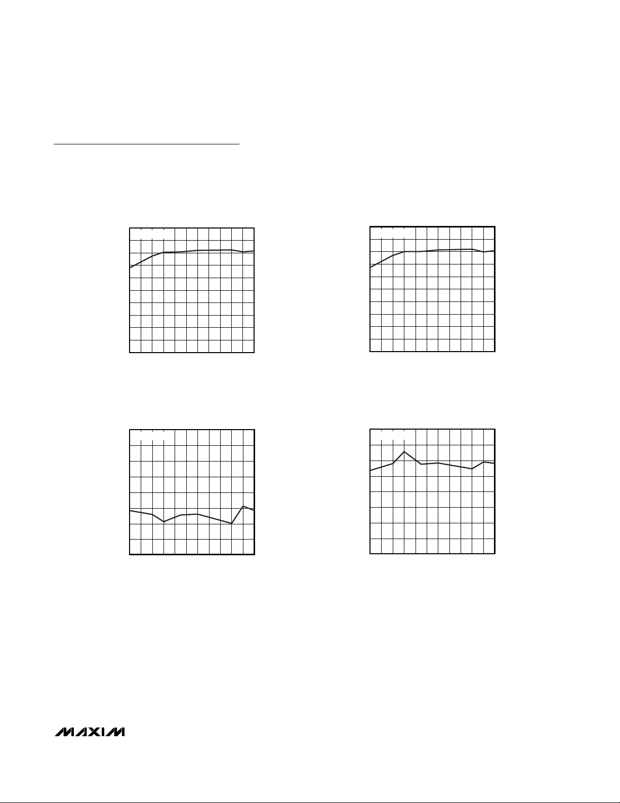
Typical Operating Characteristics
(VDD= 3.3V, OVDD= 2.0V, GND = 0, REFIN = REFOUT (internal reference), C
REFOUT
= 0.1µF, CL≈ 5pF at digital outputs, VIN= -0.5dBFS
differential input, DCE = high, CLKTYP = high, PD = low, G/T = low, f
CLK
= 65MHz (50% duty cycle), C
REFP
= C
REFN
= 0.1µF to GND, 1µF
in parallel with 10µF between REFP and REFN, C
COM
= 0.1µF in parallel with 2.2µF to GND, TA = +25°C, unless otherwise noted.)
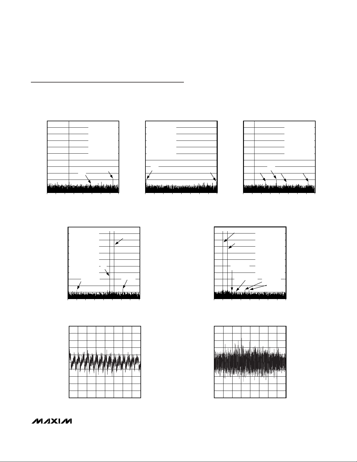
SINGLE-TONE FFT PLOT
(8192-POINT DATA RECORD)
MAX1207 toc01
FREQUENCY (MHz)
AMPLITUDE (dBFS)
282416 208124
-100
-90
-80
-70
-60
-50
-40
-30
-20
-10
0
-110
032
f
CLK
= 65.0036Msps
f
IN
= 10.006MHz
A
IN
= -0.47dBFS
SNR = 68.55dBc
SINAD = 68.50dBc
THD = -87.6dBc
SFDR = 88.5dBc
HD2
HD3
SINGLE-TONE FFT PLOT
(8192-POINT DATA RECORD)
MAX1207 toc02
FREQUENCY (MHz)
AMPLITUDE (dBFS)
282416 208124
-100
-90
-80
-70
-60
-50
-40
-30
-20
-10
0
-110
032
f
CLK
= 65.0036Msps
f
IN
= 32.367MHz
A
IN
= -0.47dBFS
SNR = 68.55dBc
SINAD = 68.50dBc
THD = -87.2dBc
SFDR = 89.0dBc
HD2
HD3
SINGLE-TONE FFT PLOT
(8192-POINT DATA RECORD)
MAX1207 toc03
FREQUENCY (MHz)
AMPLITUDE (dBFS)
282416 208124
-100
-90
-80
-70
-60
-50
-40
-30
-20
-10
0
-110
032
f
CLK
= 65.0036Msps
f
IN
= 69.995MHz
A
IN
= -0.526dBFS
SNR = 68.29dBc
SINAD = 68.23dBc
THD = -86.7dBc
SFDR = 89.0dBc
HD2
HD3
HD4
HD6
TWO-TONE FFT PLOT
(16,384-POINT DATA RECORD)
MAX1207 toc04
FREQUENCY (MHz)
AMPLITUDE (dBFS)
282416 208124
-100
-90
-80
-70
-60
-50
-40
-30
-20
-10
0
-110
032
f
CLK
= 65.0036Msps
f
IN1
= 44.0036MHz
A
IN1
= -7.0dBFS
f
IN2
= 46.0032MHz
A
IN2
= -7.0dBFS
SNR = 64.72dBc
SINAD = 64.69dBc
SFDR
TT
= 87.87dBc
IMD = -86.09dB
IM3 = -89.40dBc
f
IN1
f
IN2
f
IN1 + fIN2
f
IN1
+ 2 x f
IN2
TWO-TONE FFT PLOT
(16,384-POINT DATA RECORD)
MAX1207 toc05
FREQUENCY (MHz)
AMPLITUDE (dBFS)
282416 208124
-100
-90
-80
-70
-60
-50
-40
-30
-20
-10
0
-110
032
f
CLK
= 65.0036Msps
f
IN1
= 68.9989MHz
A
IN1
= -7.0dBFS
f
IN2
= 70.9985MHz
A
IN2
= -7.0dBFS
SNR = 64.34dBc
SINAD = 64.33dBc
SFDR
TT
= 89.17dBc
IMD = -84.38dB
IM3 = -90.16dBc
2 x f
IN2
+ f
IN1
3 x f
IN2
+ f
IN1
2 x f
IN2
+ f
IN
3 x f
IN2
+ 2 x f
IN1
f
IN1
f
IN2
INTEGRAL NONLINEARITY
MAX1207 toc06
DIGITAL OUTPUT CODE
INL (LSB)
358430722048 25601024 1536512
-0.8
-0.6
-0.4
-0.2
0
0.2
0.4
0.6
0.8
1.0
-1.0
0 4096
DIFFERENTIAL NONLINEARITY
MAX1207 toc07
DIGITAL OUTPUT CODE
DNL (LSB)
358430722048 25601024 1536512
-0.4
-0.3
-0.2
-0.1
0
0.1
0.2
0.3
0.4
0.5
-0.5
04096
Page 8
MAX1207
65Msps, 12-Bit ADC
8 _______________________________________________________________________________________
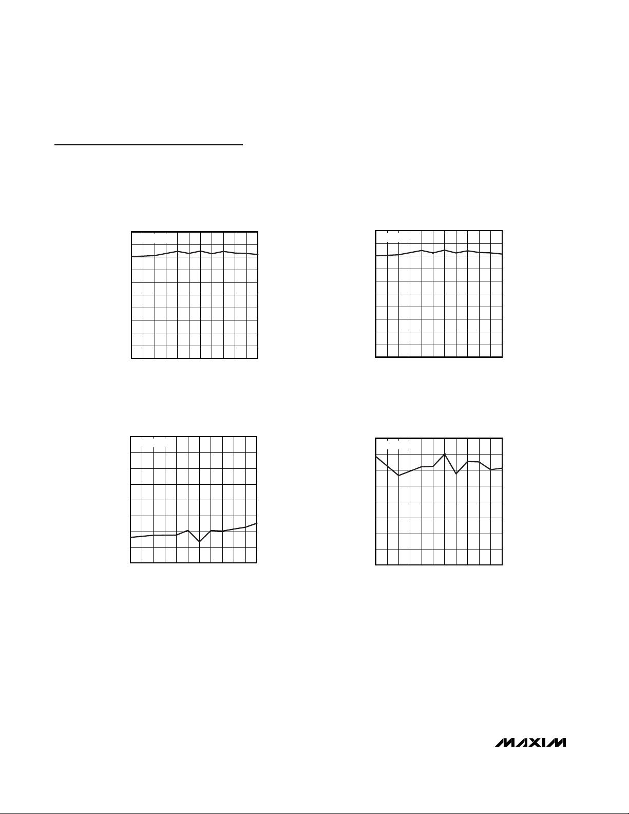
SIGNAL-TO-NOISE RATIO
vs. SAMPLING RATE
MAX1207 toc08
f
CLK
(MHz)
SNR (dB)
605545 5020 25 30 35 4015
61
62
63
64
65
66
67
68
69
70
60
10 65
fIN = 32.3MHz
SIGNAL-TO-NOISE + DISTORTION
vs. SAMPLING RATE
MAX1207 toc09
f
CLK
(MHz)
SINAD (dB)
605545 5020 25 30 35 4015
61
62
63
64
65
66
67
68
69
70
60
10 65
fIN = 32.3MHz
TOTAL HARMONIC DISTORTION
vs. SAMPLING RATE
MAX1207 toc10
f
CLK
(MHz)
THD (dBc)
605545 5020 25 30 35 4015
-95
-90
-85
-80
-75
-70
-65
-60
-100
10 65
fIN = 32.3MHz
SPURIOUS-FREE DYNAMIC RANGE
vs. SAMPLING RATE
MAX1207 toc11
f
CLK
(MHz)
SFDR (dBc)
605545 5020 25 30 35 4015
65
70
75
80
85
90
95
100
60
10 65
fIN = 32.3MHz
Typical Operating Characteristics (continued)
(VDD= 3.3V, OVDD= 2.0V, GND = 0, REFIN = REFOUT (internal reference), C
REFOUT
= 0.1µF, CL≈ 5pF at digital outputs, VIN= -0.5dBFS
differential input, DCE = high, CLKTYP = high, PD = low, G/T = low, f
CLK
= 65MHz (50% duty cycle), C
REFP
= C
REFN
= 0.1µF to GND, 1µF
in parallel with 10µF between REFP and REFN, C
COM
= 0.1µF in parallel with 2.2µF to GND, TA = +25°C, unless otherwise noted.)
Page 9
MAX1207
65Msps, 12-Bit ADC
_______________________________________________________________________________________ 9
Typical Operating Characteristics (continued)
(VDD= 3.3V, OVDD= 2.0V, GND = 0, REFIN = REFOUT (internal reference), C
REFOUT
= 0.1µF, CL≈ 5pF at digital outputs, VIN= -0.5dBFS
differential input, DCE = high, CLKTYP = high, PD = low, G/T = low, f
CLK
= 65MHz (50% duty cycle), C
REFP
= C
REFN
= 0.1µF to GND, 1µF
in parallel with 10µF between REFP and REFN, C
COM
= 0.1µF in parallel with 2.2µF to GND, TA = +25°C, unless otherwise noted.)
SIGNAL-TO-NOISE RATIO
vs. SAMPLING RATE
MAX1207 toc12
f
CLK
(MHz)
SNR (dB)
605545 5020 25 30 35 4015
61
62
63
64
65
66
67
68
69
70
60
10 65
fIN = 70.1MHz
SIGNAL-TO-NOISE + DISTORTION
vs. SAMPLING RATE
MAX1207 toc13
f
CLK
(MHz)
SINAD (dB)
605545 5020 25 30 35 4015
61
62
63
64
65
66
67
68
69
70
60
10 65
fIN = 70.1MHz
TOTAL HARMONIC DISTORTION
vs. SAMPLING RATE
MAX1207 toc14
f
CLK
(MHz)
THD (dBc)
605545 5020 25 30 35 4015
-95
-90
-85
-80
-75
-70
-65
-60
-100
10 65
fIN = 70.1MHz
SPURIOUS-FREE DYNAMIC RANGE
vs. SAMPLING RATE
MAX1207 toc15
f
CLK
(MHz)
SFDR (dBc)
605545 5020 25 30 35 4015
65
70
75
80
85
90
95
100
60
10 65
fIN = 70.1MHz
Page 10
MAX1207
65Msps, 12-Bit ADC
10 ______________________________________________________________________________________
Typical Operating Characteristics (continued)
(VDD= 3.3V, OVDD= 2.0V, GND = 0, REFIN = REFOUT (internal reference), C
REFOUT
= 0.1µF, CL≈ 5pF at digital outputs, VIN= -0.5dBFS
differential input, DCE = high, CLKTYP = high, PD = low, G/T = low, f
CLK
= 65MHz (50% duty cycle), C
REFP
= C
REFN
= 0.1µF to GND, 1µF
in parallel with 10µF between REFP and REFN, C
COM
= 0.1µF in parallel with 2.2µF to GND, TA = +25°C, unless otherwise noted.)
SIGNAL-TO-NOISE RATIO
vs. ANALOG INPUT FREQUENCY
MAX1207 toc16
ANALOG INPUT FREQUENCY (MHz)
SNR (dB)
100755025
61
62
63
64
65
66
67
68
69
70
60
0 125
SIGNAL-TO-NOISE + DISTORTION
vs. ANALOG INPUT FREQUENCY
MAX1207 toc17
ANALOG INPUT FREQUENCY (MHz)
SINAD (dB)
100755025
61
62
63
64
65
66
67
68
69
70
60
0125
TOTAL HARMONIC DISTORTION
vs. ANALOG INPUT FREQUENCY
MAX1207 toc18
ANALOG INPUT FREQUENCY (MHz)
THD (dBc)
100755025
-95
-90
-85
-80
-75
-70
-65
-60
-100
0125
SPURIOUS-FREE DYNAMIC RANGE
vs. ANALOG INPUT FREQUENCY
MAX1207 toc19
ANALOG INPUT FREQUENCY (MHz)
SFDR (dBc)
100755025
65
70
75
80
85
90
95
100
60
0125
Page 11

MAX1207
65Msps, 12-Bit ADC
______________________________________________________________________________________ 11
Typical Operating Characteristics (continued)
(VDD= 3.3V, OVDD= 2.0V, GND = 0, REFIN = REFOUT (internal reference), C
REFOUT
= 0.1µF, CL≈ 5pF at digital outputs, VIN= -0.5dBFS
differential input, DCE = high, CLKTYP = high, PD = low, G/T = low, f
CLK
= 65MHz (50% duty cycle), C
REFP
= C
REFN
= 0.1µF to GND, 1µF
in parallel with 10µF between REFP and REFN, C
COM
= 0.1µF in parallel with 2.2µF to GND, TA = +25°C, unless otherwise noted.)
SIGNAL-TO-NOSIE RATIO
vs. ANALOG INPUT POWER
MAX1207 toc20
ANALOG INPUT POWER (dBFS)
SNR (dB)
-5-10-25 -20 -15
40
45
50
55
60
65
70
75
35
-30 0
fIN = 32.129882MHz
SIGNAL-TO-NOSIE + DISTORTION
vs. ANALOG INPUT POWER
MAX1207 toc21
ANALOG INPUT POWER (dBFS)
SINAD (dB)
-5-10-25 -20 -15
40
45
50
55
60
65
70
75
35
-30 0
fIN = 32.129882MHz
TOTAL HARMONIC DISTORTION
vs. ANALOG INPUT POWER
MAX1207 toc22
ANALOG INPUT POWER (dBFS)
THD (dBc)
-5-10-25 -20 -15
-90
-85
-80
-75
-70
-65
-60
-55
-95
-30 0
fIN = 32.129882MHz
SPURIOUS-FREE DYNAMIC RANGE
vs. ANALOG INPUT POWER
MAX1207 toc23
ANALOG INPUT POWER (dBFS)
SFDR (dBc)
-5-10-25 -20 -15
60
65
70
75
80
85
90
95
55
-30 0
fIN = 32.129882MHz
Page 12

MAX1207
65Msps, 12-Bit ADC
12 ______________________________________________________________________________________
Typical Operating Characteristics (continued)
(VDD= 3.3V, OVDD= 2.0V, GND = 0, REFIN = REFOUT (internal reference), C
REFOUT
= 0.1µF, CL≈ 5pF at digital outputs, VIN= -0.5dBFS
differential input, DCE = high, CLKTYP = high, PD = low, G/T = low, f
CLK
= 65MHz (50% duty cycle), C
REFP
= C
REFN
= 0.1µF to GND, 1µF
in parallel with 10µF between REFP and REFN, C
COM
= 0.1µF in parallel with 2.2µF to GND, TA = +25°C, unless otherwise noted.)
61
64
63
62
65
66
67
68
69
70
71
20 4030 50 60 70 80
SIGNAL-TO-NOISE RATIO
vs. CLOCK DUTY CYCLE
MAX1207 toc24
CLOCK DUTY CYCLE (%)
SNR (dB)
SINGLE-ENDED CLOCK
f
IN
= 32.1271954MHz
DCE = HIGH
DCE = LOW
61
64
63
62
65
66
67
68
69
70
71
20 4030 50 60 70 80
SIGNAL-TO-NOISE + DISTORTION
vs. CLOCK DUTY CYCLE
MAX1207 toc25
CLOCK DUTY CYCLE (%)
SINAD (dB)
SINGLE-ENDED CLOCK
f
IN
= 32.1271954MHz
DCE = HIGH
DCE = LOW
-100
-90
-95
-80
-85
-70
-75
-65
20 40 5030 60 70 80
TOTAL HARMONIC DISTORTION
vs. CLOCK DUTY CYCLE
MAX1207 toc26
CLOCK DUTY CYCLE (%)
THD (dBc)
DCE = LOW
DCE = HIGH
SINGLE-ENDED CLOCK
f
IN
= 32.1271954MHz
65
75
70
85
80
95
90
100
20 40 5030 60 70 80
SPURIOUS-FREE DYNAMIC RANGE
vs. CLOCK DUTY CYCLE
MAX1207 toc27
CLOCK DUTY CYCLE (%)
SFDR (dBc)
DCE = LOW
DCE = HIGH
SINGLE-ENDED CLOCK
f
IN
= 32.1271954MHz
Page 13

MAX1207
65Msps, 12-Bit ADC
______________________________________________________________________________________ 13
Typical Operating Characteristics (continued)
(VDD= 3.3V, OVDD= 2.0V, GND = 0, REFIN = REFOUT (internal reference), C
REFOUT
= 0.1µF, CL≈ 5pF at digital outputs, VIN= -0.5dBFS
differential input, DCE = high, CLKTYP = high, PD = low, G/T = low, f
CLK
= 65MHz (50% duty cycle), C
REFP
= C
REFN
= 0.1µF to GND, 1µF
in parallel with 10µF between REFP and REFN, C
COM
= 0.1µF in parallel with 2.2µF to GND, TA = +25°C, unless otherwise noted.)
65.0
66.5
66.0
65.5
67.0
67.5
68.0
68.5
69.0
69.5
70.0
0.15 1.150.65 1.65 2.15 2.65 3.15
SIGNAL-TO-NOISE RATIO vs. ANALOG
INPUT COMMON-MODE VOLTAGE
MAX1207 toc28
ANALOG INPUT COMMON-MODE VOLTAGE (V)
SNR (dB)
fIN = 32.1271954MHz
65.0
66.5
66.0
65.5
67.0
67.5
68.0
68.5
69.0
69.5
70.0
0.15 1.150.65 1.65 2.15 2.65 3.15
SIGNAL-TO-NOISE RATIO + DISTORTION
vs. ANALOG INPUT
COMMON-MODE VOLTAGE
MAX1207 toc29
ANALOG INPUT COMMON-MODE VOLTAGE (V)
SINAD (dB)
fIN = 32.1271954MHz
-100
-90
-95
-80
-85
-75
-70
0.15 1.15 1.650.65 2.15 2.65 3.15
TOTAL HARMONIC DISTORTION
vs. ANALOG INPUT COMMON-MODE VOLTAGE
MAX1207 toc30
ANALOG INPUT COMMON-MODE VOLTAGE (V)
THD (dBc)
fIN = 32.1271954MHz
70
80
75
90
85
95
100
0.15 1.15 1.650.65 2.15 2.65 3.15
SPURIOUS-FREE DYNAMIC RANGE
vs. ANALOG INPUT COMMON-MODE VOLTAGE
MAX1207 toc31
ANALOG INPUT COMMON-MODE VOLTAGE (V)
SFDR (dBc)
fIN = 32.1271954MHz
Page 14

MAX1207
65Msps, 12-Bit ADC
14 ______________________________________________________________________________________
Typical Operating Characteristics (continued)
(VDD= 3.3V, OVDD= 2.0V, GND = 0, REFIN = REFOUT (internal reference), C
REFOUT
= 0.1µF, CL≈ 5pF at digital outputs, VIN= -0.5dBFS
differential input, DCE = high, CLKTYP = high, PD = low, G/T = low, f
CLK
= 65MHz (50% duty cycle), C
REFP
= C
REFN
= 0.1µF in parallel
with 10µF to GND, 10µF between REFP and REFN, C
COM
= 0.1µF in parallel with 2.2µF to GND, TA = +25°C, unless otherwise noted.)
SIGNAL-TO-NOISE RATIO
vs. TEMPERATURE
MAX1207 toc32
TEMPERATURE (°C)
SNR (dB)
603510-15
61
62
63
64
65
66
67
68
69
70
60
-40 85
fIN = 32.35893MHz
SIGNAL-TO-NOISE + DISTORTION
vs. TEMPERATURE
MAX1207 toc33
TEMPERATURE (°C)
SINAD (dB)
603510-15
61
62
63
64
65
66
67
68
69
70
60
-40 85
fIN = 32.35893MHz
TOTAL HARMONIC DISTORTION
vs. TEMPERATURE
MAX1207 toc34
TEMPERATURE (°C)
THD (dBc)
603510-15
-95
-90
-85
-80
-75
-70
-100
-40 85
fIN = 32.35893MHz
SPURIOUS-FREE DYNAMIC RANGE
vs. TEMPERATURE
MAX1207 toc35
TEMPERATURE (°C)
SFDR (dBc)
603510-15
75
80
85
90
95
100
70
-40 85
fIN = 32.35893MHz
Page 15

MAX1207
65Msps, 12-Bit ADC
______________________________________________________________________________________ 15
OFFSET ERROR
vs. TEMPERATURE
MAX1207 toc36
TEMPERATURE (°C)
OFFSET ERROR (%FS)
603510-15
-0.26
-0.22
-0.18
-0.24
-0.20
-0.16
-0.14
-0.12
-0.28
-40 85
V
REFIN
= 2.048V
GAIN ERROR
vs. TEMPERATURE
MAX1207 toc37
TEMPERATURE (°C)
GAIN ERROR (%FR)
603510-15
0.10
0.20
0.30
0.15
0.25
0.35
0.40
0
-40 85
V
REFIN
= 2.048V
Pin Description
PIN NAME FUNCTION
1 REFP
Positive Reference I/O. Conversion range is ±(V
REFP
- V
REFN
). Bypass REFP to GND with a 0.1µF
capacitor. Connect a 1µF capacitor in parallel with a 10µF capacitor between REFP and REFN.
2 REFN
Negative Reference I/O. Conversion range is ±(V
REFP
- V
REFN
). Bypass REFN to GND with a 0.1µF
capacitor. Connect a 1µF capacitor in parallel with a 10µF capacitor between REFP and REFN.
3 COM
Common-Mode Voltage I/O. Bypass COM to GND with a ≥2.2µF capacitor in parallel with a 0.1µF
capacitor.
4, 7, 16, 35
GND Ground. Connect all ground pins and the EP together.
5 INP
Positive Analog Input. For single-ended input operation, connect signal source to INP and connect INN
to COM. For differential operation, connect the input signal between INP and INN.
6INN
Negative Analog Input. For single-ended input operation, connect INN to COM. For differential operation,
connect the input signal between INP and INN.
8 DCE
Duty-Cycle Equalizer Input. Connect DCE low (GND) to disable the internal duty-cycle equalizer.
Connect DCE high (OV
DD
or VDD) to enable the internal duty-cycle equalizer.
9 CLKN
Negative Clock Input. In differential clock input mode (CLKTYP = OV
DD
or VDD), connect the clock
signal between CLKP and CLKN. In single-ended clock mode (CLKTYP = GND), apply the clock signal
to CLKP and connect CLKN to GND.
10 CLKP
Positive Clock Input. In differential clock input mode (CLKTYP = OV
DD
or VDD), connect the differential
clock signal between CLKP and CLKN. In single-ended clock mode (CLKTYP = GND), apply the singleended clock signal to CLKP and connect CLKN to GND.
Typical Operating Characteristics (continued)
(VDD= 3.3V, OVDD= 2.0V, GND = 0, REFIN = REFOUT (internal reference), C
REFOUT
= 0.1µF, CL≈ 5pF at digital outputs, VIN= -0.5dBFS
differential input, DCE = high, CLKTYP = high, PD = low, G/T = low, f
CLK
= 65MHz (50% duty cycle), C
REFP
= C
REFN
= 0.1µF to GND, 1µF
in parallel with 10µF between REFP and REFN, C
COM
= 0.1µF in parallel with 2.2µF to GND, TA = +25°C, unless otherwise noted.)
Page 16
MAX1207
65Msps, 12-Bit ADC
16 ______________________________________________________________________________________
Pin Description (continued)
PIN NAME FUNCTION
11
Clock Type Definition Input. Connect CLKTYP to GND to define the single-ended clock input. Connect
CLKTYP to OV
DD
or VDD to define the differential clock input.
12–15, 36
V
DD
Analog Power Input. Connect VDD to a 3.0V to 3.6V power supply. Bypass VDD to GND with a parallel
capacitor combination of ≥2.2µF and 0.1µF. Connect all V
DD
pins to the same potential.
17, 34 OV
DD
Output Driver Power Input. Connect OVDD to a 1.7V to VDD power supply. Bypass OVDD to GND with a
parallel capacitor combination of ≥2.2µF and 0.1µF.
18 DOR
Data Out-of-Range Indicator. The DOR digital output indicates when the analog input voltage is out of
range. When DOR is high, the analog input is beyond its full-scale range. When DOR is low, the analog
input is within its full-scale range.
19 D11 CMOS Digital Output, Bit 11 (MSB)
20 D10 CMOS Digital Output, Bit 10
21 D9 CMOS Digital Output, Bit 9
22 D8 CMOS Digital Output, Bit 8
23 D7 CMOS Digital Output, Bit 7
24 D6 CMOS Digital Output, Bit 6
25 D5 CMOS Digital Output, Bit 5
26 D4 CMOS Digital Output, Bit 4
27 D3 CMOS Digital Output, Bit 3
28 D2 CMOS Digital Output, Bit 2
29 D1 CMOS Digital Output, Bit 1
30 D0 CMOS Digital Output, Bit 0 (LSB)
31, 32 I. C. Internally Connected. Leave I. C. unconnected.
33 DAV
Data Valid Output. The DAV is a single-ended version of the input clock that is compensated to correct
for any input clock duty-cycle variations. The MAX1211 evaluation kit (MAX1211EVKIT) utilizes DAV to
latch data (D0–D11) into external back-end digital circuitry.
37 PD Power-Down Input. Force PD high for power-down mode. Force PD low for normal operation.
38
Internal Reference Voltage Output. For internal reference operation, connect REFOUT directly to REFIN
or use a resistive-divider from REFOUT to set the voltage at REFIN. Bypass REFOUT to GND with a
≥0.1µF capacitor.
39 REFIN Reference Input. V
REFIN
= 2 x (V
REFP
- V
REFN
). Bypass REFIN to GND with a ≥0.1µF capacitor.
40 G/T
Output Format Select Input. Connect G/T to GND for the two’s complement digital output format. Connect
G/T to OV
DD
or VDD for the Gray code digital output format.
—EP
Exposed Paddle. EP is internally connected to GND. Externally connect EP to GND to achieve specified
performance.
CLKTYP
REFOUT
Page 17
MAX1207
65Msps, 12-Bit ADC
______________________________________________________________________________________ 17
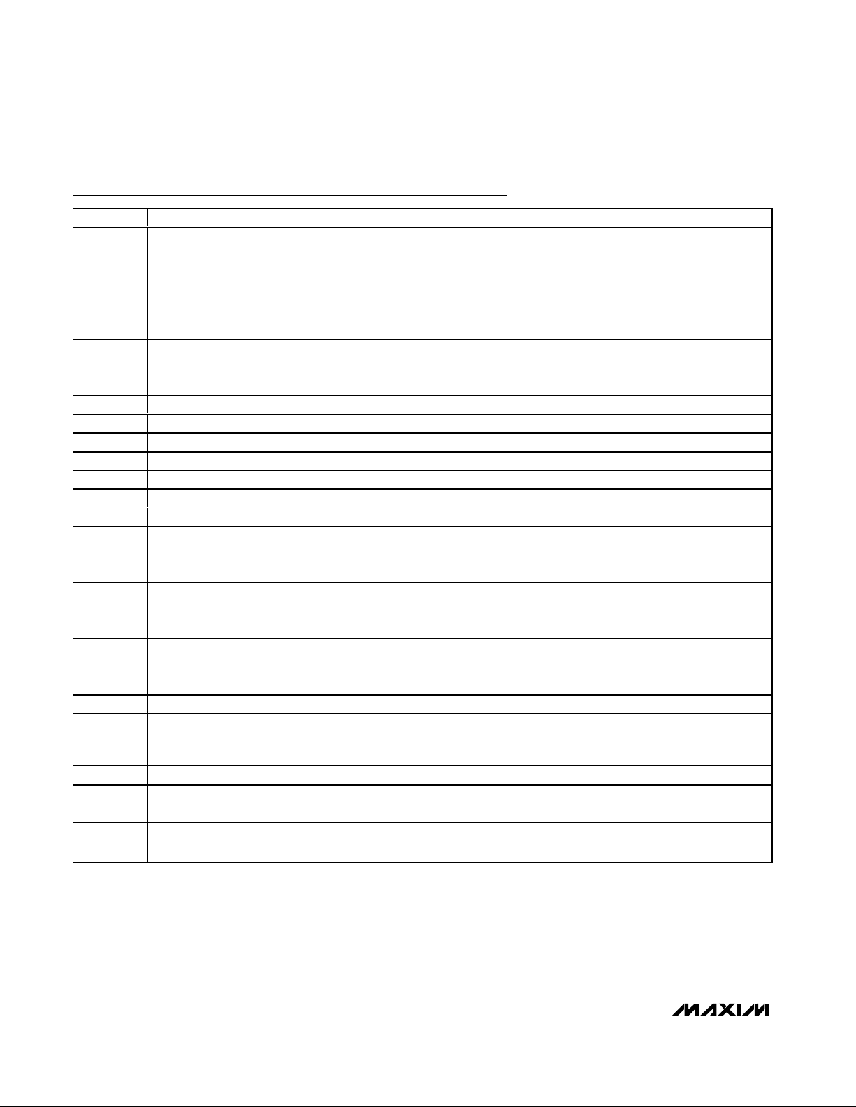
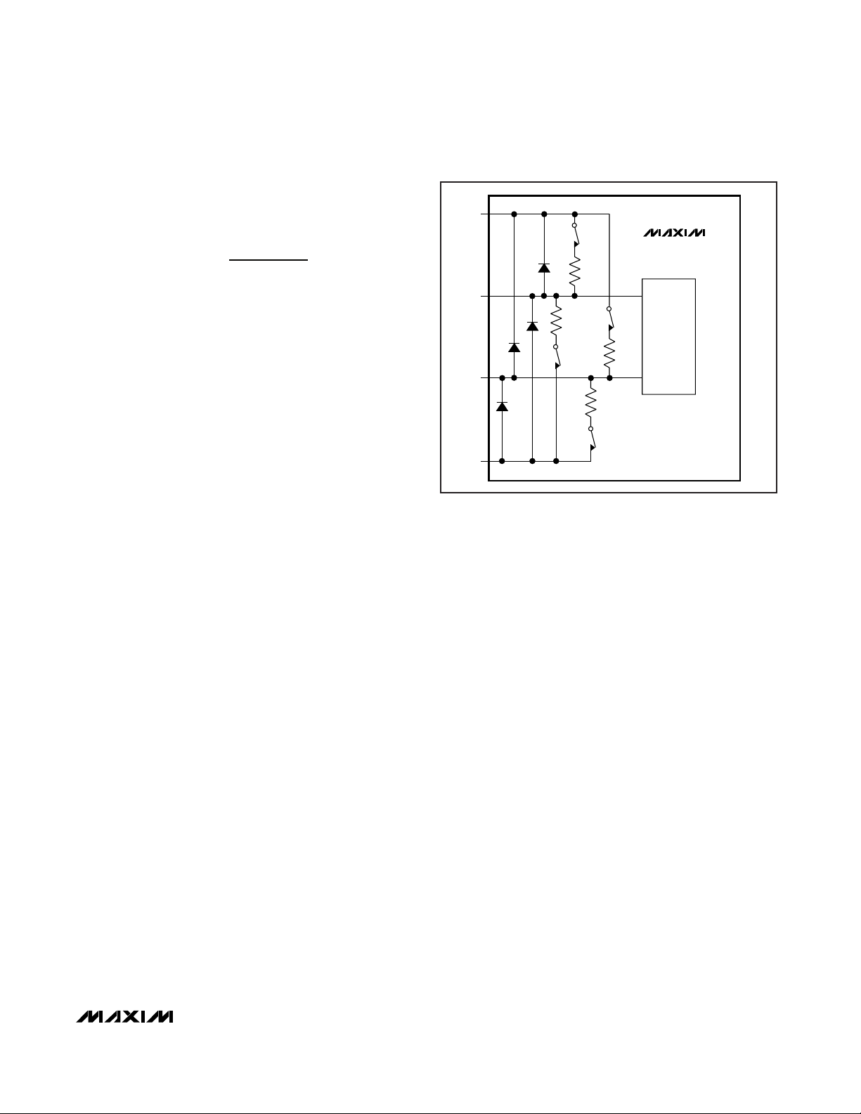
Detailed Description
The MAX1207 uses a 10-stage, fully differential,
pipelined architecture (Figure 1) that allows for highspeed conversion while minimizing power consumption. Samples taken at the inputs move progressively
through the pipeline stages every half clock cycle.
From input to output, the total clock-cycle latency is 8.5
clock cycles.
Each pipeline converter stage converts its input voltage
into a digital output code. At every stage, except the
last, the error between the input voltage and the digital
output code is multiplied and passed along to the next
pipeline stage. Digital error correction compensates for
ADC comparator offsets in each pipeline stage and
ensures no missing codes. Figure 2 shows the
MAX1207 functional diagram.
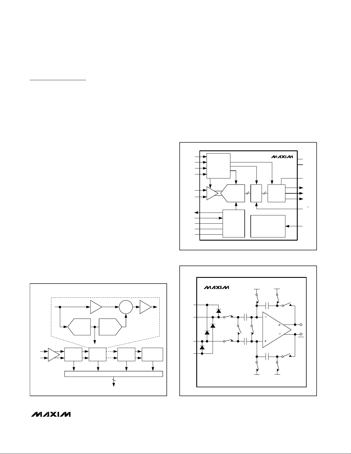
Input Track-and-Hold (T/H) Circuit
Figure 3 displays a simplified functional diagram of the
input T/H circuits. In track mode, switches S1, S2a,
S2b, S4a, S4b, S5a, and S5b are closed. The fully differential circuits sample the input signals onto the two
capacitors (C2a and C2b) through switches S4a and
S4b. S2a and S2b set the common mode for the operational transconductance amplifier (OTA), and open
simultaneously with S1, sampling the input waveform.
Switches S4a, S4b, S5a, and S5b are then opened
before switches S3a and S3b connect capacitors C1a
and C1b to the output of the amplifier and switch S4c is
closed. The resulting differential voltages are held on
capacitors C2a and C2b. The amplifiers charge capacitors C1a and C1b to the same values originally held on
C2a and C2b. These values are then presented to the
first-stage quantizers and isolate the pipelines from the
fast-changing inputs. The wide input-bandwidth T/H
amplifier allows the MAX1207 to track and sample/hold
analog inputs of high frequencies well beyond Nyquist.
Analog input INP to INN can be driven either differentially or single ended. For differential inputs, balance
the input impedance of INP and INN and set the common-mode voltage to midsupply (V
DD
/ 2) for optimum
performance.
CLOCK
GENERATOR
AND
DUTY-CYCLE
EQUALIZER
INP
INN
12-BIT
PIPELINE
ADC
DEC
REFERENCE
SYSTEM
COM
REFOUT
REFN
REFP
OV
DD
DAV
OUTPUT
DRIVERS
D0–D11
DOR
G/T
REFIN
POWER CONTROL
AND
BIAS CIRCUITS
CLKP
CLKN
CLKTYP
PD
V
DD
GND
T/H
DCE
MAX1207
Figure 2. Functional Diagram
S3b
S3a
CML
SWITCHES SHOWN IN TRACK MODE
S5b
S5a
V
DD
INP
INN
GND
S1
OUT
OUT
C2a
C2b
S4c
S4a
S4b
C1b
C1a
INTERNAL
BIAS
INTERNAL
BIAS
CML
S2a
S2b
OTA
MAX1207
Figure 3. Internal T/H Circuit
INP
INN
STAGE 1
GAIN OF 8
4 BITS 1.5 BITS 1.5 BITS
1.5 BITS
D0–D11
1 BIT
DIGITAL ERROR CORRECTION
T/H
T/H
FLASH
ADC
DAC
x2
+
-
∑
STAGE 2
GAIN OF 2
STAGE 10
END OF PIPE
STAGE 9
GAIN OF 2
Figure 1. Pipeline Architecture—Stage Blocks
Page 18
MAX1207
65Msps, 12-Bit ADC
18 ______________________________________________________________________________________
Reference Output (REFOUT)
An internal bandgap reference is the basis for all the
internal voltages and bias currents used in the
MAX1207. The power-down logic input (PD) enables
and disables the reference circuit. REFOUT has
approximately 17kΩ to GND when the MAX1207 is in
power-down. The reference circuit requires 10ms to
power up and settle when power is applied to the
MAX1207 or when PD transitions from high to low.
The internal bandgap reference and buffer generate
REFOUT to be 2.048V with a +100ppm/°C temperature
coefficient. Connect an external ≥0.1µF bypass capacitor from REFOUT to GND for stability. REFOUT sources
up to 1.4mA and sinks up to 100µA for external circuits
with a load regulation of 35mV/mA. Short-circuit protection limits I
REFOUT
to a 2.1mA source current when
shorted to GND and a 240µA sink current when shorted
to VDD.
Analog Inputs and Reference
Configurations
The MAX1207 full-scale analog input range is ±V
REF
with a common-mode input range of V
DD
/ 2 ±0.8V.
V
REF
is the difference between V
REFP
and V
REFN
. The
MAX1207 provides three modes of reference operation.
The voltage at REFIN (V
REFIN
) sets the reference oper-
ation mode (Table 1).
To operate the MAX1207 with the internal reference, connect REFOUT to REFIN either with a direct short or
through a resistive-divider. In this mode, COM, REFP, and
REFN are low-impedance outputs with V
COM
= V
DD
/ 2,
V
REFP
= V
DD
/ 2 + V
REFIN
/ 4, and V
REFN
= V
DD
/ 2 -
V
REFIN
/ 4. The REFIN input impedance is very large
(>50MΩ). When driving REFIN through a resistive-divider,
use resistances ≥10kΩ to avoid loading REFOUT.
Buffered external reference mode is virtually identical to
internal reference mode except that the reference
source is derived from an external reference and not
the MAX1207 REFOUT. In buffered external reference
mode, apply a stable 0.7V to 2.3V source at REFIN.
COM, REFP, and REFN are low-impedance outputs
with V
COM
= V
DD
/ 2, V
REFP
= V
DD
/ 2 + V
REFIN
/ 4, and
V
REFN
= V
DD
/ 2 - V
REFIN
/ 4.
To operate the MAX1207 in unbuffered external reference mode, connect REFIN to GND. Connecting REFIN
to GND deactivates the on-chip reference buffers for
COM, REFP, and REFN. With their buffers deactivated,
COM, REFP, and REFN inputs must be driven through
separate, external reference sources. Drive V
COM
to
V
DD
/ 2 ±5%, and drive REFP and REFN such that
V
COM
= (V
REFP
+ V
REFN
) / 2. The analog input range is
±(V
REFP
- V
REFN
).
All three modes of reference operation require the same
bypass capacitor combination. Bypass COM with a
0.1µF capacitor in parallel with a ≥2.2µF capacitor to
GND. Bypass REFP and REFN each with a 0.1µF capacitor to GND. Bypass REFP to REFN with a 1µF capacitor
in parallel with a 10µF capacitor. Place the 1µF capacitor
as close to the device as possible. Bypass REFIN and
REFOUT to GND with a 0.1µF capacitor.
For detailed circuit suggestions, see Figures 12 and 13.
Clock Input and Clock Control Lines
(CLKP, CLKN, CLKTYP, DCE)
The MAX1207 accepts both differential and singleended clock inputs. For single-ended clock input operation, connect CLKTYP to GND, CLKN to GND, and drive
CLKP with the external single-ended clock signal. For
differential clock input operation, connect CLKTYP to
OVDDor VDDand drive CLKP and CLKN with the external differential clock signal. To reduce clock jitter, the
external single-ended clock must have sharp falling
edges. Consider the clock input as an analog input and
route it away from any other analog inputs and digital
signal lines.
CLKP and CLKN are high impedance when the
MAX1207 is powered down (Figure 4).
Low clock jitter is required for the specified SNR performance of the MAX1207. Analog input sampling occurs
on the falling edge of the clock signal, requiring this
V
REFIN
REFERENCE MODE
35% V
REFOUT
to 100% V
REFOUT
In t e r n a l re f e r e n c e m o d e . RE FIN i s d r i ven b y RE FOU T ei ther thr oug h a d i r ect shor t or a r esi sti ve
d i vi d er . V
C OM
= V
D D
/ 2, V
RE F P
= V
D D
/ 2 + V
RE F IN
/ 4, and V
RE F N
= V
D D
/ 2 - V
RE F IN
/ 4.
0.7V to 2.3V
Buffered external reference mode. An external 0.7V to 2.3V reference voltage is applied
to REFIN. V
COM
= V
DD
/ 2, V
REFP
= V
DD
/ 2 + V
REFIN
/ 4, and V
REFN
= V
DD
/ 2 - V
REFIN
/ 4.
<0.5V
Unbuffered external reference mode. REFP, REFN, and COM are driven by external
reference sources. V
REF
is the difference between the externally applied V
REFP
and V
REFN
.
Table 1. Reference Modes
Page 19
MAX1207
65Msps, 12-Bit ADC
______________________________________________________________________________________ 19
edge to have the lowest possible jitter. Jitter limits the
maximum SNR performance of any ADC according to
the following relationship:
where fINrepresents the analog input frequency and t
J
is the total system clock jitter. Clock jitter is especially
critical for undersampling applications. For example,
assuming that clock jitter is the only noise source, to
obtain the specified 68.5dB of SNR with an input frequency of 32.5MHz, the system must have less than
1.8ps of clock jitter.
Clock Duty-Cycle Equalizer (DCE)
The MAX1207 clock duty-cycle equalizer allows for a
wide 20% to 80% clock duty cycle when enabled (DCE
= OV
DD
or VDD). When disabled (DCE = GND), the
MAX1207 accepts a narrow 45% to 65% clock duty
cycle. See the Typical Operating Characteristics section
for Dynamic Performance vs. Clock Duty-Cycle plots.
The clock duty-cycle equalizer uses a delay-locked
loop to create internal timing signals that are duty-cycle
independent. Due to this delay-locked loop, the
MAX1207 requires approximately 100 clock cycles to
acquire and lock to new clock frequencies.
Disabling the clock duty-cycle equalizer reduces the
analog supply current by 1.5mA.
System Timing Requirements
Figure 5 shows the relationship between the clock, analog inputs, DAV indicator, DOR indicator, and the resulting output data. The analog input is sampled on the
falling edge of the clock signal and the resulting data
appears at the digital outputs 8.5 clock cycles later.
The DAV indicator is synchronized with the digital output and optimized for use in latching data into digital
back-end circuitry. Alternatively, digital back-end circuitry can be latched with the falling edge of the clock.
Data Valid Output (DAV)
DAV is a single-ended version of the input clock
(CLKP). The output data changes on the falling edge of
DAV, and DAV rises once the output data is valid.
The state of the duty-cycle equalizer input (DCE)
changes the waveform at DAV. With the duty-cycle
equalizer disabled (DCE low), the DAV signal is the
inverse of the signal at CLKP delayed by 6.4ns. With
the duty-cycle equalizer enabled (DCE high), the DAV
signal has a fixed pulse width that is independent of
CLKP. In either case, with DCE high or low, output data
at D0–D11 and DOR are valid from 8.5ns before the ris-
ing edge of DAV to 6.3ns after the rising edge of DAV,
and the rising edge of DAV is synchronized to have a
6.4ns delay from the falling edge of CLKP.
DAV is high impedance when the MAX1207 is in
power-down (PD = high). DAV is capable of sinking
and sourcing 600µA and has three times the drive
strength of D0–D11 and DOR. DAV is typically used to
latch the MAX1207 output data into an external backend digital circuit.
Keep the capacitive load on DAV as low as possible
(<25pF) to avoid large digital currents feeding back into
the analog portion of the MAX1207 and degrading its
dynamic performance. An external buffer on DAV isolates
it from heavy capacitive loads. Refer to the MAX1211
evaluation kit schematic for an example of DAV driving
back-end digital circuitry through an external buffer.
Data Out-of-Range Indicator (DOR)
The DOR digital output indicates when the analog input
voltage is out of range. When DOR is high, the analog
input is out of range. When DOR is low, the analog
input is within range. The valid differential input range is
from (V
REFP
- V
REFN
) to (V
REFN
- V
REFP
). Signals outside this valid differential range cause DOR to assert
high as shown in Table 2.
DOR is synchronized with DAV and transitions along
with output data D0–D11. There is an 8.5 clock-cycle
latency in the DOR function just as with the output data
(Figure 5).
SNR
ft
IN J
=×
×× ×
20
1
2
log
π
10kΩ
10kΩ
10kΩ
10kΩ
SWITCHES S
1_
AND S2_ ARE OPEN
DURING POWER-DOWN, MAKING
CLKP AND CLKN HIGH IMPEDANCE.
SWITCHES S
2_
ARE OPEN IN
SINGLE-ENDED CLOCK MODE.
V
DD
CLKP
CLKN
GND
S
1H
S
2H
S
1L
S
2L
DUTY-
CYCLE
EQUALIZER
MAX1207
Figure 4. Simplified Clock Input Circuit
Page 20

MAX1207
65Msps, 12-Bit ADC
20 ______________________________________________________________________________________
GRAY CODE
OUTPUT CODE
(G/TTTT = 1)
TWO’S COMPLEMENT
OUTPUT CODE
(G/TTTT = 0)
BINARY
D11 D0
OF
D11 D0
DECIMAL
OF
D11 D0
(CODE
10
)
BINARY
D11 D0
OF
D11 D0
DECIMAL
OF
D11 D0
(CODE
10
)
V
IN P
- V
IN N
V
REFP
= 2.162 V
V
REFN
= 1.138 V
1000 0000 0000
0x800 +4095
0x7FF +2047
>+1.0235V
(DATA OUT OF
RANGE)
1000 0000 0000
0x800 +4095
0x7FF +2047 +1.0235V
1000 0000 0001
0x801 +4094
0x7FE +2046 +1.0230V
1100 0000 0011
0xC03 +2050
0x002 +2 +0.0010V
1100 0000 0001
0xC01 +2049
0x001 +1 +0.0005V
1100 0000 0000
0xC00 +2048
0x000 0 +0.0000V
0100 0000 0000
0x400 +2047
0xFFF -1 -0.0005V
0100 0000 0001
0x401 +2046
0xFFE -2 -0.0010V
0000 0000 0001
0x001 +1
0x801 -2047 -1.0235V
0000 0000 0000
0x000 0
0x800 -2048 -1.0240V
0000 0000 0000
0x000 0
0x800 -2048
<-1.0240V
(DATA OUT OF
RANGE)
)
Table 2. Output Codes vs. Input Voltage
DAV
D0–D11
(V
REFP
- V
REFN
)
(V
REFN
- V
REFP
)
N + 4
N + 5
N + 6
N - 2
N - 3
DOR
8.5 CLOCK-CYCLE DATA LATENCY
DIFFERENTIAL ANALOG INPUT (INP - INN)
CLKN
CLKP
t
AD
t
CL
t
CH
t
SETUP
t
SETUP
t
HOLD
t
HOLD
t
DAV
NN + 1N + 2 N + 3 N + 5 N + 6 N + 7N - 1N - 2N - 3 N + 9N + 8N + 4
N
N + 1
N + 2
N + 3
N + 7
N + 8
N + 9
N - 1
Figure 5. System Timing Diagram
HEXADECIMAL
EQUIVALENT
DOR
EQUIVALENT
HEXADECIMAL
EQUIVALENT
DOR
(
EQUIVALENT
1
0
0
0
0
0
0
0
0
0
1
0111 1111 1111 1
0111 1111 1111 0
0111 1111 1110 0
0000 0000 0010 0
0000 0000 0001 0
0000 0000 0000 0
1111 1111 1111 0
1111 1111 1110 0
1000 0000 0001 0
1000 0000 0000 0
1000 0000 0000 1
Page 21
MAX1207
65Msps, 12-Bit ADC
______________________________________________________________________________________ 21
DOR is high impedance when the MAX1207 is in
power-down (PD = high). DOR enters a high-impedance state within 10ns of the rising edge of PD and
becomes active within 10ns of PD’s falling edge.
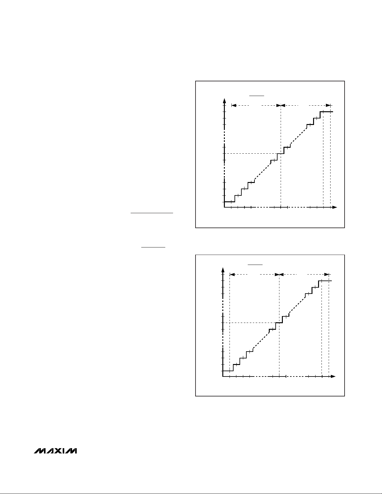
Digital Output Data (D0–D11), Output Format (G/T)
The MAX1207 provides a 12-bit, parallel, tri-state output bus. D0–D11 and DOR update on the falling edge
of DAV and are valid on the rising edge of DAV.
The MAX1207 output data format is either Gray code or
two’s complement, depending on the logic input G/T.
With G/T high, the output data format is Gray code.
With G/T low, the output data format is two’s complement. See Figure 8 for a binary-to-Gray and Gray-tobinary code-conversion example.
The following equations, Table 2, Figure 6, and Figure 8
define the relationship between the digital output and
the analog input:
for Gray code (G/T = 1).
for two’s complement (G/T = 0).
where CODE
10
is the decimal equivalent of the digital
output code as shown in Table 2.
The digital outputs D0–D11 are high impedance when
the MAX1207 is in power-down (PD = high). D0–D11
go high impedance within 10ns of the rising edge of PD
and become active within 10ns of PD’s falling edge.
Keep the capacitive load on the MAX1207 digital outputs D0–D11 as low as possible (<15pF) to avoid large
digital currents feeding back into the analog portion of
the MAX1207 and degrading its dynamic performance.
The addition of external digital buffers on the digital outputs isolate the MAX1207 from heavy capacitive loads.
To improve the dynamic performance of the MAX1207,
add 220Ω resistors in series with the digital outputs
close to the MAX1207. Refer to the MAX1211 evaluation
kit schematic for an example of the digital outputs driving a digital buffer through 220Ω series resistors.
Power-Down Input (PD)
The MAX1207 has two power modes that are controlled
with the power-down digital input (PD). With PD low, the
MAX1207 is in its normal operating mode. With PD
high, the MAX1207 is in power-down mode.
The power-down mode allows the MAX1207 to efficiently use power by transitioning to a low-power state when
conversions are not required. Additionally, the
MAX1207 parallel output bus goes high impedance in
power-down mode, allowing other devices on the bus
to be accessed.
VV V V
CODE
INP INN REFP REFN
− = − ××()2
4096
10
VV V V
CODE
INP INN REFP REFN
− = − ××
−
()2
2048
4096
10
DIFFERENTIAL INPUT VOLTAGE (LSB)
-1-2045
4096
2 x V
REF
1 LSB =
V
REF
= V
REFP
- V
REFN
V
REF
V
REF
0+1-2047 +2047+2045
TWO'S COMPLEMENT OUTPUT CODE (LSB)
0x800
0x801
0x802
0x803
0x7FF
0x7FE
0x7FD
0xFFF
0x000
0x001
Figure 6. Two’s Complement Transfer Function (G/T= 0)
DIFFERENTIAL INPUT VOLTAGE (LSB)
-1-2045
4096
2 x V
REF
1 LSB =
V
REF
= V
REFP
- V
REFN
V
REF
V
REF
0+1-2047 +2047+2045
GRAY OUTPUT CODE (LSB)
0x000
0x001
0x003
0x002
0x800
0x801
0x803
0x400
0xC00
0xC01
Figure 7. Gray Code Transfer Function (G/T= 1)
Page 22
MAX1207
65Msps, 12-Bit ADC
22 ______________________________________________________________________________________
BINARY-TO-GRAY CODE CONVERSION
1) THE MOST SIGNIFICANT GRAY-CODE BIT IS THE SAME
AS THE MOST SIGNIFICANT BINARY BIT.
0111 0100 1100 BINARY
GRAY CODE0
2) SUBSEQUENT GRAY-CODE BITS ARE FOUND ACCORDING
TO THE FOLLOWING EQUATION:
D11 D7 D3 D0
GRAYX = BINARYX +BINARY
X + 1
BIT POSITION
0111 0100 1100 BINARY
GRAY CODE0
D11 D7 D3 D0
BIT POSITION
GRAY
10
= BINARY10BINARY
11
GRAY10 = 1 0
GRAY
10
= 1
1
3) REPEAT STEP 2 UNTIL COMPLETE
01 11 0100 1100 BINARY
GRAY CODE0
D11 D7 D3 D0
BIT POSITION
GRAY
9
= BINARY9BINARY
10
GRAY9 = 1 1
GRAY
9
= 0
10
4) THE FINAL GRAY CODE CONVERSTION IS:
0111 0100 1100 BINARY
GRAY CODE0
D11 D7 D3 D0
BIT POSITION
100 1101 1010
GRAY-TO-BINARY CODE CONVERSION
1) THE MOST SIGNIFICANT BINARY BIT IS THE SAME AS THE
MOST SIGNIFICANT GRAY-CODE BIT.
2) SUBSEQUENT BINARY BITS ARE FOUND ACCORDING TO
THE FOLLOWING EQUATION:
D11 D7 D3 D0
BINARYX = BINARY
X+1
BIT POSITION
BINARY
10
= BINARY11GRAY
10
BINARY10 = 0 1
BINARY
10
= 1
3) REPEAT STEP 2 UNTIL COMPLETE
4) THE FINAL BINARY CONVERSTION IS:
0100 1110 1010
BINARY
GRAY CODE
D11 D7 D3 D0
BIT POSITION
0BINARY
GRAY CODE0100 11 011010
BINARY
9
= BINARY10GRAY
9
BINARY9 = 1 0
BINARY
9
= 1
GRAY
X
01001110 1010
BINARY
GRAY CODE
0
D11 D7 D3 D0
BIT POSITION
1
01 00 1110 1010
BINARY
GRAY CODE
0
D11 D7 D3 D0
BIT POSITION
11
0111 0100 1100
AB Y=AB
00
01
10
11
0
1
1
0
EXCULSIVE OR TRUTH TABLE
WHERE IS THE EXCLUSIVE OR FUNCTION (SEE TRUTH
TABLE BELOW) AND X IS THE BIT POSITION.
+
WHERE IS THE EXCLUSIVE OR FUNCTION (SEE TRUTH
TABLE BELOW) AND X IS THE BIT POSITION.
+
+
+
+
+
+
+
+
+
+
+
+
+
+
+
Figure 8. Binary-to-Gray and Gray-to-Binary Code Conversion
Page 23
MAX1207
65Msps, 12-Bit ADC
______________________________________________________________________________________ 23
In power-down mode, all internal circuits are off, the
analog supply current reduces to 0.045A, and the digital supply current reduces to 6µA. The following list
shows the state of the analog inputs and digital outputs
in power-down mode:
• INP, INN analog inputs are disconnected from the
internal input amplifier (Figure 3).
• REFOUT has approximately 17kΩ to GND.
• REFP, COM, REFN go high impedance with respect
to VDDand GND, but there is an internal 4kΩ resis-
tor between REFP and COM, as well as an internal
4kΩ resistor between REFN and COM.
• D0–D11, DOR, and DAV go high impedance.
• CLKP, CLKN clock inputs go high impedance
(Figure 4).
The wake-up time from power-down mode is dominated by the time required to charge the capacitors at
REFP, REFN, and COM. In internal reference mode and
buffered external reference mode, the wake-up time is
typically 10ms. When operating in the unbuffered external reference mode, the wake-up time is dependent on
the external reference drivers.
Applications Information
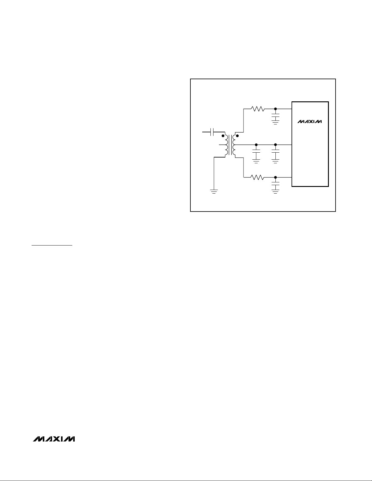
Using Transformer Coupling
In general, the MAX1207 provides better SFDR and
THD with fully differential input signals than singleended input drive. In differential input mode, evenorder harmonics are lower as both inputs are balanced,
and each of the ADC inputs only requires half the signal swing compared to single-ended input mode.
An RF transformer (Figure 9) provides an excellent
solution to convert a single-ended input source signal
to a fully differential signal, required by the MAX1207
for optimum performance. Connecting the center tap of
the transformer to COM provides a V
DD
/ 2 DC level
shift to the input. Although a 1:1 transformer is shown, a
step-up transformer can be selected to reduce the
drive requirements. A reduced signal swing from the
input driver, such as an op amp, can also improve the
overall distortion. The configuration of Figure 9 is good
for input frequencies up to Nyquist (f
CLK
/ 2).
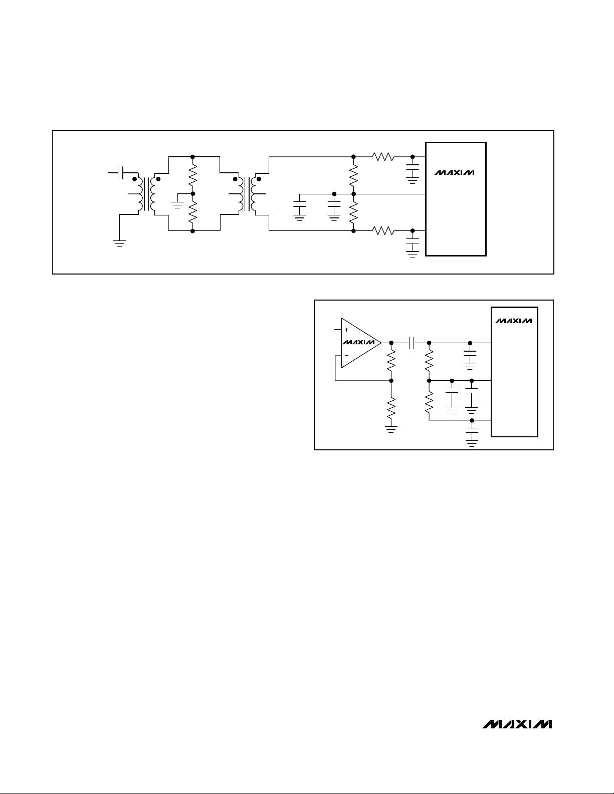
The circuit of Figure 10 converts a single-ended input
signal to fully differential just as in Figure 9. However,
Figure 10 utilizes an additional transformer to improve
the common-mode rejection, allowing high-frequency
signals beyond the Nyquist frequency. The two sets of
49.9Ω termination resistors provide an equivalent 50Ω
termination to the signal source. The second set of ter-
mination resistors connects to COM, providing the correct input common-mode voltage. Two 0Ω resistors in
series with the analog inputs allow high IF input frequencies. These 0Ω resistors can be replaced with lowvalue resistors to limit the input bandwidth.
Single-Ended AC-Coupled Input Signal
Figure 11 shows an AC-coupled, single-ended input
application. The MAX4108 provides high speed, high
bandwidth, low noise, and low distortion to maintain the
input signal integrity.
Buffered External Reference Drives
Multiple ADCs
The buffered external reference mode allows for more
control over the MAX1207 reference voltage and allows
multiple converters to use a common reference. The
REFIN input impedance is >50MΩ.
Figure 12 shows the MAX6062 precision bandgap reference used as a common reference for multiple converters. The 2.048V output of the MAX6062 passes
through a one-pole 10Hz lowpass filter to the MAX4250.
The MAX4250 buffers the 2.048V reference before its
output is applied to the REFIN input of the MAX1207.
The MAX4250 provides a low offset voltage (for high
gain accuracy) and a low noise level.
MAX1207
T1
N.C.
V
IN
6
1
5
2
4
3
12pF
12pF
0.1µF
0.1µF
2.2µF
24.9
Ω
24.9
Ω
MINICIRCUITS
TT1-6
OR
T1-1T
INN
COM
INP
Figure 9. Transformer-Coupled Input Drive for Input
Frequencies Up to Nyquist
Page 24
MAX1207
65Msps, 12-Bit ADC
24 ______________________________________________________________________________________
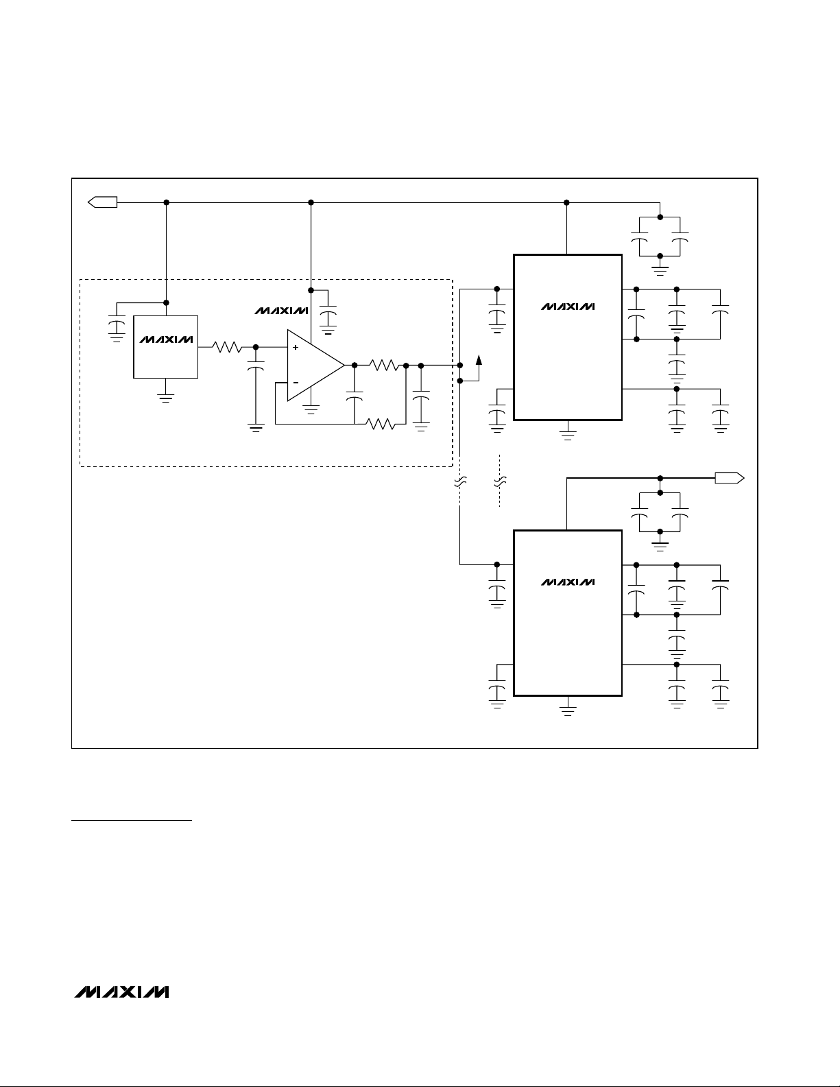
Unbuffered External Reference Drives
Multiple ADCs
The unbuffered external reference mode allows for precise control over the MAX1207 reference and allows
multiple converters to use a common reference.
Connecting REFIN to GND disables the internal reference, allowing REFP, REFN, and COM to be driven
directly by a set of external reference sources.
Figure 13 shows the MAX6066 precision bandgap reference used as a common reference for multiple converters. The 2.500V output of the MAX6066 is followed
by a 10Hz lowpass filter and precision voltage-divider.
The MAX4254 buffers the taps of this divider to provide
the +2.000V, +1.500V, and +1.000V sources to drive
REFP, REFN, and COM. The MAX4254 provides a low
offset voltage and low noise level. The individual voltage followers are connected to 10Hz lowpass filters,
which filter both the reference voltage and amplifier
noise to a level of 3nV/√Hz. The 2.000V and 1.000V ref-
erence voltages set the differential full-scale range of
the associated ADCs at ±1.000V.
The common power supply for all active components
removes any concern regarding power-supply
sequencing when powering up or down.
With the outputs of the MAX4254 matching better than
0.1%, the buffers and subsequent lowpass support as
many as 8 ADCs.
Grounding, Bypassing, and Board Layout
The MAX1207 requires high-speed board layout design
techniques. Refer to the MAX1211 evaluation kit data
sheet for a board layout reference. Locate all bypass
capacitors as close to the device as possible, preferably on the same side as the ADC, using surfacemount devices for minimum inductance. Bypass V
DD
to
GND with a 0.1µF ceramic capacitor in parallel with a
2.2µF ceramic capacitor. Bypass OVDDto GND with a
0.1µF ceramic capacitor in parallel with a 2.2µF ceramic capacitor.
Multilayer boards with ample ground and power planes
produce the highest level of signal integrity. All
MAX1207 GNDs and the exposed backside paddle
must be connected to the same ground plane. The
MAX1207 relies on the exposed backside paddle connection for a low-inductance ground connection. Use
multiple vias to connect the top-side ground to the bottom-side ground. Isolate the ground plane from any
noisy digital system ground planes such as a DSP or
output buffer ground.
Route high-speed digital signal traces away from the
sensitive analog traces. Keep all signal lines short and
free of 90° turns.
Ensure that the differential analog input network layout
is symmetric and that all parasitics are balanced equally. Refer to the MAX1211 evaluation kit data sheet for
an example of symmetric input layout.
MAX1207
0.1µF
100Ω
100Ω
12pF
12pF
INP
INN
COM
0.1µF
V
IN
MAX4108
24.9Ω
24.9Ω
2.2µF
Figure 11. Single-Ended, AC-Coupled Input Drive
MAX1207
T1
N.C.
V
IN
6
1
5
2
4
3
12pF
12pF
0.1µF
0Ω*
49.9
Ω
0.5%
49.9
Ω
0.5%
0Ω*
MINICIRCUITS
ADT1-1WT
T1
N.C. N.C.
6
1
5
2
4
3
MINICIRCUITS
ADT1-1WT
INP
COM
INN
*0Ω RESISTORS CAN BE REPLACED WITH
LOW-VALUE RESISTORS TO LIMIT THE
INPUT BANDWIDTH.
0.1µF4.7µF
49.9
Ω
0.5%
49.9
Ω
0.5%
Figure 10. Transformer-Coupled Input Drive for Input Frequencies Beyond Nyquist
Page 25
MAX1207
65Msps, 12-Bit ADC
______________________________________________________________________________________ 25
Parameter Definitions
Integral Nonlinearity (INL)
Integral nonlinearity is the deviation of the values on an
actual transfer function from a straight line. This straight
line is either a best-straight-line fit or a line drawn
between the end points of the transfer function, once
offset and gain errors have been nullified. The static linearity parameters for the MAX1207 are guaranteed by
design using the best-straight-line fit method.
Differential Nonlinearity (DNL)
Differential nonlinearity is the difference between an
actual step width and the ideal value of 1 LSB. A DNL
error specification of less than 1 LSB guarantees no
missing codes and a monotonic transfer function.
Offset Error
Ideally, the midscale MAX1207 transition occurs at 0.5
LSB above midscale. The offset error is the amount of
deviation between the measured transition point and
the ideal transition point.
16.2kΩ
47Ω
+3.3V
2
2.048V
REFIN
REFP
REFN
COMREFOUT
GND
4
2
3
5
1
1
39
38
39
38
2
3
1
2
3
1
1µF
0.1µF
V
DD
NOTE: ONE FRONT-END REFERENCE CIRCUIT PROVIDES ±15mA OF OUTPUT DRIVE.
* PLACE AS CLOSE TO THE DEVICE AS POSSIBLE.
3
0.1µF
+3.3V
0.1µF
2.2µF
0.1µF
0.1µF
0.1µF
0.1µF
0.1µF
10µF
2.2µF
MAX6062
MAX1207
REFIN
REFP
REFN
COMREFOUT
GND
V
DD
0.1µF
2.2µF
0.1µF
0.1µF
*1µF
0.1µF
0.1µF
0.1µF
10µF
2.2µF
MAX1207
10µF
6V
47µF
6V
1.47kΩ
MAX4250
*1µF
Figure 12. External Buffered (MAX4250) Reference Drive Using a MAX6062 Bandgap Reference
Page 26

MAX1207
65Msps, 12-Bit ADC
26 ______________________________________________________________________________________
21.5kΩ
1%
21.5kΩ
1%
21.5kΩ
1%
21.5kΩ
1%
21.5kΩ
1%
1MΩ
1MΩ
47Ω
1.47kΩ
+3.3V
2
REFP
REFN
COM
REFOUT
GND
2
3
1/4
MAX4254
2.000V
1
1
39
38
39
38
2
3
1
1µF
10µF
6V
0.1µF
V
DD
3
330µF
6V
+3.3V
UNCOMMITTED
NOTE: ONE FRONT-END REFERENCE CIRCUIT
SUPPORTS UP TO 8 MAX1207s.
+3.3V
0.1µF
2.2µF
0.1µF
*1µF
0.1µF
0.1µF
0.1µF
10µF
2.2µF
MAX1207
MAX6066
2.500V
REFIN
REFIN
REFP
REFN
COM
REFOUT
GND
V
DD
0.1µF
2.2µF
0.1µF
*1µF
0.1µF
0.1µF
0.1µF
10µF
2.2µF
MAX1207
47Ω
1.47kΩ
6
5
1/4
MAX4254
1.500V
7
10µF
6V
330µF
6V
47Ω
1.47kΩ
9
10
1/4
MAX4254
1.000V
8
10µF
6V
330µF
6V
11
12
13
4
14
0.1µF
MAX4254
1/4
1
2
3
* PLACE AS CLOSE TO THE DEVICE AS POSSIBLE.
Figure 13. External Unbuffered Reference Driving 8 ADCs with MAX4254 and MAX6066
Page 27

MAX1207
65Msps, 12-Bit ADC
______________________________________________________________________________________ 27
Gain Error
Ideally, the positive full-scale MAX1207 transition
occurs at 1.5 LSB below positive full scale, and the
negative full-scale transition occurs at 0.5 LSB above
negative full scale. The gain error is the difference of
the measured transition points minus the difference of
the ideal transition points.
Aperture Jitter
Figure 14 depicts the aperture jitter (tAJ), which is the
sample-to-sample variation in the aperture delay.
Aperture Delay
Aperture delay (tAD) is the time defined between the
rising edge of the sampling clock and the instant when
an actual sample is taken (Figure 14).
Overdrive Recovery Time
Overdrive recovery time is the time required for the
ADC to recover from an input transient that exceeds the
full-scale limits. The MAX1207 specifies overdrive
recovery time using an input transient that exceeds the
full-scale limits by ±10%.
Signal-to-Noise Ratio (SNR)
For a waveform perfectly reconstructed from digital
samples, the theoretical maximum SNR is the ratio of
the full-scale analog input (RMS value) to the RMS
quantization error (residual error). The ideal, theoretical
minimum analog-to-digital noise is caused by quantization error only and results directly from the ADC’s resolution (N bits):
SNR
dB[max]
= 6.02dB× N + 1.76
dB
In reality, there are other noise sources besides quantization noise: thermal noise, reference noise, clock jitter,
etc. SNR is computed by taking the ratio of the RMS
signal to the RMS noise. RMS noise includes all spectral components to the Nyquist frequency excluding the
fundamental, the first six harmonics (HD2–HD7), and
the DC offset.
Signal-to-Noise Plus Distortion (SINAD)
SINAD is computed by taking the ratio of the RMS signal to the RMS noise plus distortion. RMS noise plus
distortion includes all spectral components to the
Nyquist frequency, excluding the fundamental and the
DC offset.
Effective Number of Bits (ENOB)
ENOB specifies the dynamic performance of an ADC at a
specific input frequency and sampling rate. An ideal
ADC’s error consists of quantization noise only. ENOB for
a full-scale sinusoidal input waveform is computed from:
Total Harmonic Distortion (THD)
THD is the ratio of the RMS sum of the first six harmonics of the input signal to the fundamental itself. This is
expressed as:
where V1is the fundamental amplitude, and V2through
V7are the amplitudes of the 2nd- through 7th-order
harmonics (HD2–HD7).
Single-Tone Spurious-Free
Dynamic Range (SFDR)
SFDR is the ratio expressed in decibels of the RMS
amplitude of the fundamental (maximum signal component) to the RMS amplitude of the next-largest spurious
component, excluding DC offset.
Two-Tone Spurious-Free
Dynamic Range (SFDR
TT
)
SFDRTTrepresents the ratio, expressed in decibels,
of the RMS amplitude of either input tone to the RMS
amplitude of the next-largest spurious component in
the spectrum, excluding DC offset. This spurious
component can occur anywhere in the spectrum up
to Nyquist and is usually an intermodulation product
or a harmonic.
THD
VVVVVV
V
=×
+++++
20
22324252627
2
1
log
ENOB
SINAD=−
176
602..
t
AD
T/H TRACKHOLD HOLD
CLKN
CLKP
ANALOG
INPUT
SAMPLED
DATA
t
AJ
Figure 14. T/H Aperture Timing
Page 28

MAX1207
65Msps, 12-Bit ADC
28 ______________________________________________________________________________________
Intermodulation Distortion (IMD)
IMD is the ratio of the RMS sum of the intermodulation
products to the RMS sum of the two fundamental input
tones. This is expressed as:
The fundamental input tone amplitudes (V1and V2)
are at -7dBFS. Fourteen intermodulation products
(V
IMP_
) are used in the MAX1207 calculation. The
intermodulation products are the amplitudes of the
output spectrum at the following frequencies:
• 2nd-order intermodulation products: f1 + f2, f2 - f1
• 3rd-order intermodulation products: 2 x f1 - f2, 2 x f2
- f1, 2 x f1 + f2, 2 x f2 + f1
• 4th-order intermodulation products: 3 x f1 - f2, 3 x f2
- f1, 3 x f1 + f2, 3 x f2 + f1
• 5th-order intermodulation products: 3 x f1 - 2 x f2, 3
x f2 - 2 x f1, 3 x f1 + 2 x f2, 3 x f2 + 2 x f1
3rd-Order Intermodulation (IM3)
IM3 is the total power of the 3rd-order intermodulation
products to the Nyquist frequency relative to the total
input power of the two input tones f1 and f2. The individual input tone levels are at -7dBFS. The 3rd-order
intermodulation products are 2 x f1 - f2, 2 x f2 - f1, 2 x
f1 + f2, 2 x f2 + f1.
Chip Information
TRANSISTOR COUNT: 18,700
PROCESS: CMOS
IMD x
VV V
VV
IMP IMP IMPn
=
++
+
••• •
20
1
2
2
22
122
2
log
D0
D1
EXPOSED PADDLE (GND)
D3
D4
D7
D8
D9
D5
D6
D2
COM
GND
INP
INN
GND
DCE
CLKN
CLKP
REFN
REFP
1
2
3
4
5
6
7
8
9
10
111213141516171819
20
403938373635343332
31
30
29
28
27
26
25
24
23
22
21
V
DD
GND
OV
DD
D11
D10
V
DDVDDVDD
CLKTYP
REFIN
REFOUTPDV
DD
GND
OVDDDAV
I.C.
I.C.
G/T
THIN QFN
6mm × 6mm × 0.8mm
MAX1207
DOR
TOP VIEW
Pin Configuration
Page 29

MAX1207
65Msps, 12-Bit ADC
Maxim cannot assume responsibility for use of any circuitry other than circuitry entirely embodied in a Maxim product. No circuit patent licenses are
implied. Maxim reserves the right to change the circuitry and specifications without notice at any time.
Maxim Integrated Products, 120 San Gabriel Drive, Sunnyvale, CA 94086 408-737-7600 ____________________ 29
© 2004 Maxim Integrated Products Printed USA is a registered trademark of Maxim Integrated Products.
Package Information
(The package drawing(s) in this data sheet may not reflect the most current specifications. For the latest package outline information,
go to www.maxim-ic.com/packages
.)
Note: For the MAX1207 exposed pad variations, the package code is T4066-3.
QFN THIN 6x6x0.8.EPS
e e
LL
A1 A2
A
E/2
E
D/2
D
E2/2
E2
(NE-1) X e
(ND-1) X e
e
D2/2
D2
b
k
k
L
C
L
C
L
C
L
C
L
E
1
2
21-0141
PACKAGE OUTLINE
36, 40, 48L THIN QFN, 6x6x0.8mm
L1
L
e
8. COPLANARITY APPLIES TO THE EXPOSED HEAT SINK SLUG AS WELL AS THE TERMINALS.
6. ND AND NE REFER TO THE NUMBER OF TERMINALS ON EACH D AND E SIDE RESPECTIVELY.
5. DIMENSION b APPLIES TO METALLIZED TERMINAL AND IS MEASURED BETWEEN 0.25 mm AND 0.30 mm
FROM TERMINAL TIP.
4. THE TERMINAL #1 IDENTIFIER AND TERMINAL NUMBERING CONVENTION SHALL CONFORM TO JESD 95-1
SPP-012. DETAILS OF TERMINAL #1 IDENTIFIER ARE OPTIONAL, BUT MUST BE LOCATED WITHIN THE
ZONE INDICATED. THE TERMINAL #1 IDENTIFIER MAY BE EITHER A MOLD OR MARKED FEATURE.
9. DRAWING CONFORMS TO JEDEC MO220, EXCEPT FOR 0.4mm LEAD PITCH PACKAGE T4866-1.
7. DEPOPULATION IS POSSIBLE IN A SYMMETRICAL FASHION.
3. N IS THE TOTAL NUMBER OF TERMINALS.
2. ALL DIMENSIONS ARE IN MILLIMETERS. ANGLES ARE IN DEGREES.
1. DIMENSIONING & TOLERANCING CONFORM TO ASME Y14.5M-1994.
NOTES:
10. WARPAGE SHALL NOT EXCEED 0.10 mm.
E
2
2
21-0141
PACKAGE OUTLINE
36, 40, 48L THIN QFN, 6x6x0.8mm
 Loading...