

Page 1
MAX1201
+5V Single-Supply, 2.2Msps, 14-Bit
Self-Calibrating ADC
________________________________________________________________
Maxim Integrated Products
1
For free samples & the latest literature: http://www.maxim-ic.com, or phone 1-800-998-8800.
For small orders, phone 1-800-835-8769.
General Description
The MAX1201 is a 14-bit, monolithic, analog-to-digital
converter (ADC) capable of conversion rates up to
2.2Msps. This integrated circuit, built on a CMOS
process, uses a fully differential, pipelined architecture
with digital error correction and a short self-calibration
procedure that corrects for capacitor and gain mismatches and ensures 14-bit linearity at full sample rates.
An on-chip track-and-hold (T/H) maintains superb
dynamic performance up to the Nyquist frequency. The
MAX1201 operates from a single +5V supply.
The fully differential inputs allow an input swing of
±VREF. A single-ended input is also possible using two
operational amplifiers. The reference is also differential
with the positive reference (RFPF) typically connected
to +4.096V and the negative reference (RFNF) tied to
analog ground. Additional sensing pins (RFPS, RFNS)
are provided to compensate for any resistive divider
action that may occur due to finite internal and external
resistances.
The power dissipation is typically only 269mW at +5V
and a sampling rate of 2.2Msps. The device employs a
CMOS compatible, 14-bit parallel, two’s complement output data format. The MAX1201 is available in a 44-pin
MQFP package and is specified over the commercial
temperature (0°C to +70°C) and extended (-40°C to
+85°C) temperature ranges.
Applications
xDSL
Instrumentation
Medical Imaging
Scanners
IR Imaging
Spectrum Analysis
Features
♦ Monolithic 14-Bit, 2.2Msps ADC
♦ Signal-to-Noise Ratio of 83dB
♦ Spurious-Free Dynamic Range of 91dB
♦ Differential Nonlinearity Error: ±0.3LSB
♦ Integral Nonlinearity Error: ±1.2LSB
♦ Single +5V Analog Supply, +3V Digital Supply
♦ Low Power Dissipation: 269mW
♦ On-Demand Self-Calibration
♦ Three-State, Two’s Complement Output Data
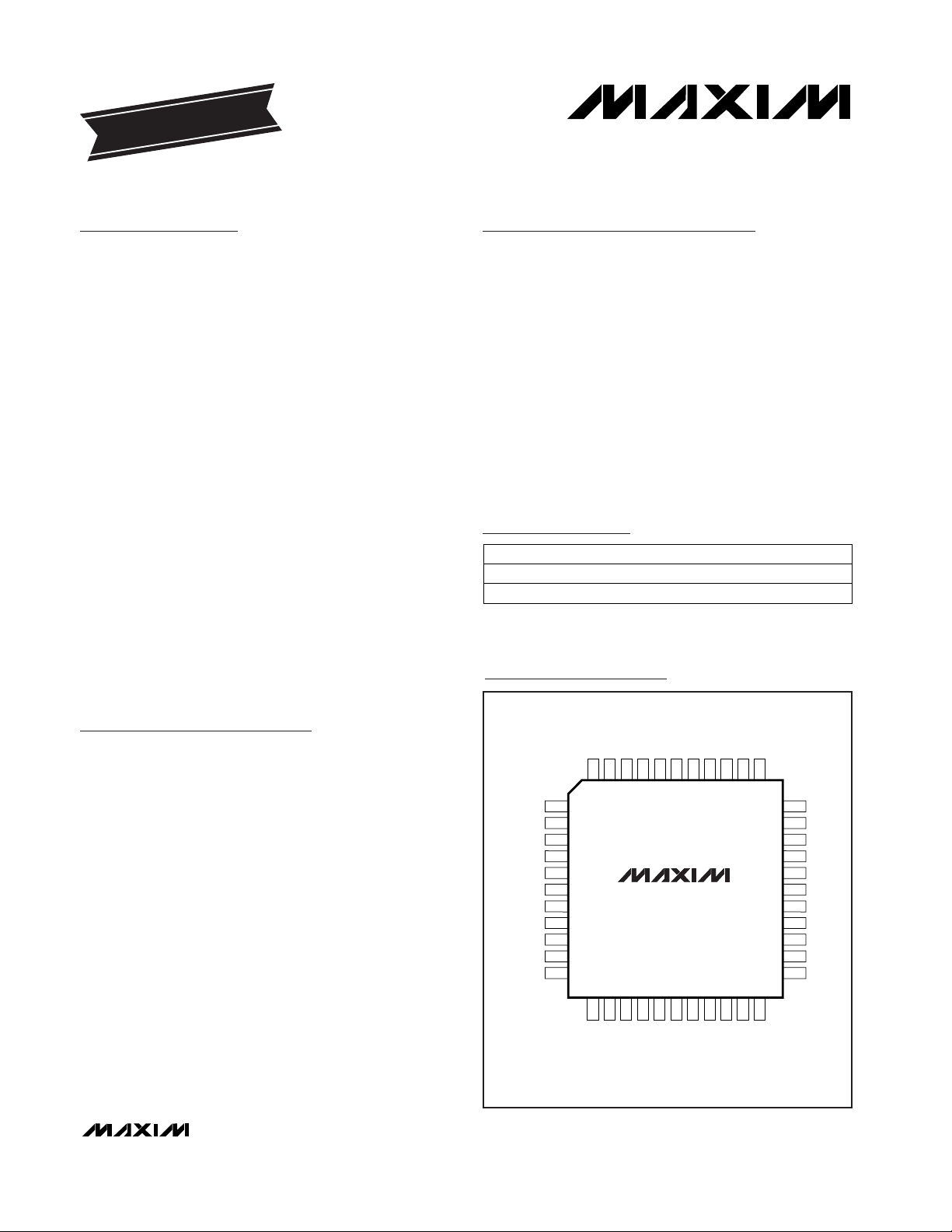
OE
DAV
CLK
DV
DD
DGND
DGND
DV
DD
TEST1
TEST2
TEST3
D0
ST_CAL
AGND
AV
DD
AGND
AGND
AV
DD
DOR
D13
D12
D11
D10
1
2
3
4
5
6
7
8
9
10
11
1213141516171819202122
4443424140393837363534
33
32
31
30
29
28
27
26
25
24
23
D9D8D7
D6
DRV
DD
DGND
D5D4D3D2D1
END_CAL
INN
N.C.
N.C.
INP
RFNS
RFNF
RFPS
RFPFCMTEST0
TOP VIEW
MQFP
MAX1201
19-4776; Rev 1; 11/98
PART TEMP. RANGE PIN-PACKAGE
Ordering Information
Pin Configuration
MAX1201CMH
MAX1201EMH -40°C to +85°C
0°C to +70°C 44 MQFP
44 MQFP
EVALUATION KIT
AVAILABLE
Page 2
MAX1201
+5V Single-Supply, 2.2Msps, 14-Bit
Self-Calibrating ADC
2 _______________________________________________________________________________________
ABSOLUTE MAXIMUM RATINGS
ELECTRICAL CHARACTERISTICS
(AVDD= +5V ±5%, DV
DD
= DRV
DD
= +3.3V, V
RFPS
= +4.096V, V
RFNS
= AGND, VCM= +2.048, VIN= -0.5dBFS, f
CLK
= 4.5056MHz,
digital output load ≤ 20pF, TA= T
MIN
to T
MAX
= 0°C to +70°C, unless otherwise noted. Typical values are at TA= +25°C.) (Note 1)
Stresses beyond those listed under “Absolute Maximum Ratings” may cause permanent damage to the device. These are stress ratings only, and functional
operation of the device at these or any other conditions beyond those indicated in the operational sections of the specifications is not implied. Exposure to
absolute maximum rating conditions for extended periods may affect device reliability.
AVDDto AGND, DGND..........................................................+7V
DV
DD
to DGND, AGND..........................................................+7V
DRV
DD
to DGND, AGND .......................................................+7V
INP, INN, RFPF, RFPS,
RFNF, RFNS, CLK, CM..........(AGND - 0.3V) to (AV
DD
+ 0.3V)
Digital Inputs to DGND............................-0.3V to (DV
DD
+ 0.3V)
Digital Output (DAV) to DGND..............-0.3V to (DRV
DD
+ 0.3V)
Other Digital Outputs to DGND.............-0.3V to (DRV
DD
+ 0.3V)
Continuous Power Dissipation (TA= +70°C)
44-Pin MQFP (derate 11.11mW/°C above +70°C).......889mW
Operating Temperature Ranges (T
A
)
MAX1201CMH ....................................................0°C to +70°C
MAX1201EMH .................................................-40°C to +85°C
Storage Temperature Range.............................-65°C to +160°C
Lead Temperature (soldering, 10sec).............................+300°C
PARAMETER SYMBOL MIN TYP MAX UNITS
Reference Voltage (Note 3) V
REF
4.096 4.5
V
Input Capacitance C
I
21
pF
Input Resistance (Note 4) R
I
25
kΩ
Reference Input Resistance
700 1000
Ω
Input Voltage Range (Notes 2, 3) V
IN
4.096 4.5
V
±4.096 ±4.5
CONDITIONS
Per side in Track Mode
Single-ended
Differential
Input-Referred Noise
75
µV
RMS
Gain Error
-5 -1.7 +5
%FSR
Offset Error
-0.1 ±0.004 +0.1
%FSR
Maximum Sampling Rate f
SAMPLE
2.2528
Msps
Conversion Time (Pipeline
Delay/Latency)
4
f
SAMPLE
Cycles
Integral Nonlinearity
Resolution
(no missing codes; Note 5)
RES
14
Bits
INL
±1.2
LSB
Differential Nonlinearity DNL
-1 ±0.3 +1
LSB
f
CLK
f
SAMPLE
=
f
CLK
/
2
After calibration, guaranteed
Small-Signal Bandwidth
78
MHz
Full-Power Bandwidth
3.3
MHz
Overvoltage Recovery Time
Acquisition Time t
ACQ
100
ns
t
OVR
410
ns
Aperture Delay t
AD
3
ns
To full-scale step (0.006%)
Page 3
MAX1201
+5V Single-Supply, 2.2Msps, 14-Bit
Self-Calibrating ADC
_______________________________________________________________________________________ 3
ELECTRICAL CHARACTERISTICS (continued)
(AVDD= +5V ±5%, DV
DD
= DRV
DD
= +3.3V, V
RFPS
= +4.096V, V
RFNS
= AGND, VCM= +2.048, VIN= -0.5dBFS, f
CLK
= 4.5056MHz,
digital output load ≤ 20pF, TA= T
MIN
to T
MAX
= 0°C to +70°C, unless otherwise noted. Typical values are at TA= +25°C.) (Note 1)
dB
55Gain
55Offset
PSRRPower-Supply Rejection Ratio
sec0.1Warm-Up Time
mW269 380PDSSPower Dissipation
10pF loads on D0–D13 and DAV mA0.3 1I(DRVDD)Output Drive Supply Current
V3DV
DD
DRV
DD
Output Drive Supply Voltage
V4.75 5 5.25AV
DD
Analog Supply Voltage
V3 5.25DV
DD
Digital Supply Voltage
mA12I(DVDD)Digital Supply Current
fIN= 1.0021MHz
fIN= 502.7kHz
fIN= 100.1kHz
fIN= 1.0021MHz
fIN= 502.7kHz
fIN= 100.1kHz
fIN= 1.0021MHz
fIN= 502.7kHz
fIN= 100.1kHz
fIN= 502.7kHz
fIN= 1.0021MHz
fIN= 100.1kHz
86
Spurious-Free Dynamic Range
(Note 5)
89SFDR dB
84 91
78
79
dB
-88 -80
THD
Total Harmonic Distortion
(Note 6)
-85
-83
dB
77 82
SINAD
Signal-to-Noise Ratio +
Distortion (Note 5)
81
82 dB
78 83
SNR
Signal-to-Noise Ratio
(Note 5)
CONDITIONS UNITSMIN TYP MAXSYMBOLPARAMETER
mA53 75I(AVDD)Analog Supply Current
POWER REQUIREMENTS
CL= 20pF
CONDITIONS
ns85 113.5 137t
CH
Clock High Time
ns227t
CLK
ns4/f
SAMPLE
t
CONV
Conversion Time
Clock Period
ns16 75t
REL
Bus Relinquish Time
ns16 75t
AC
Data Access Time
ns85 113.5 137t
CL
Clock Low Time
ns70 150t
OD
Output Delay
ns1/f
CLK
t
DAV
DAV Pulse Width
ns65 145t
S
CLK-to-DAV Rising Edge
UNITSMIN TYP MAXSYMBOLPARAMETER
TIMING CHARACTERISTICS
(AVDD= +5V, DVDD= DRVDD= +3.3V, f
CLK
= 4.5056MHz, TA= T
MIN
to T
MAX
= 0°C to +70°C, unless otherwise noted. Typical
values are at T
A
= +25°C.) (Note 1)
ST_CAL = DV
DD
f
CLK
cycles
17,400t
CAL
Calibration Time
Page 4
MAX1201
+5V Single-Supply, 2.2Msps, 14-Bit
Self-Calibrating ADC
4 _______________________________________________________________________________________
DIGITAL INPUT AND OUTPUT CHARACTERISTICS
(AVDD= +5V, DVDD= DRVDD= +3.3V, TA= T
MIN
to T
MAX
, unless otherwise noted. Typical values are at TA= +25°C.)
Note 1: Reference inputs driven by operational amplifiers for Kelvin-sensed operation.
Note 2: For unipolar mode, the analog input voltage, V
INP
, must be within 0V and V
REF
, V
INN
= V
REF
/2; where V
REF
= V
RFPS
-
V
RFNS
. For differential mode, the analog input voltages V
INP
and V
INN
must be within 0V and V
REF
; where V
REF
= V
RFPS
-
V
RFNS
. The common-mode voltage of the inputs INP and INN is V
REF
/2.
Note 3: Minimum and maximum parameters are not tested. Guaranteed by design.
Note 4: Input resistance varies inversely with sample rate.
Note 5: Calibration remains valid for temperature changes within ±20°C and power-supply variations ±5%.
Note 6: All AC specifications are shown for the differential mode.
I
SOURCE
= 200µA
V
IN_
= DV
DD
V
IN_
= 0
CONDITIONS
4.0Input Capacitance
DVDD- 0.8V
IH
0.8V
IL
Input Low Voltage
Input High Voltage
DV
DD
DV
DD
- 0.4 - 0.03
V
OH
Output High Voltage
0.8CLK
VIL
CLK Input Low Voltage
AVDD- 0.8CLK
VIH
CLK Input High Voltage
9C
CLK
CLK Input Capacitance
±0.1 ±10
I
IN
Digital Input Current
MIN TYP MAX
SYMBOLPARAMETER
I
SINK
= 1.6mA 70 400V
OL
Output Low Voltage
±0.1 ±10I
LEAKAGE
Three-State Leakage Current
3.5C
OUT
Three-State Output Capacitance
mV
µA
pF
pF
V
V
V
V
V
pF
µA
UNITS
±0.1 ±10
V
IN_
= 0 or DV
DD
±1 ±10I
CLK
CLK Input Current µA
Page 5
MAX1201
+5V Single-Supply, 2.2Msps, 14-Bit
Self-Calibrating ADC
_______________________________________________________________________________________
5
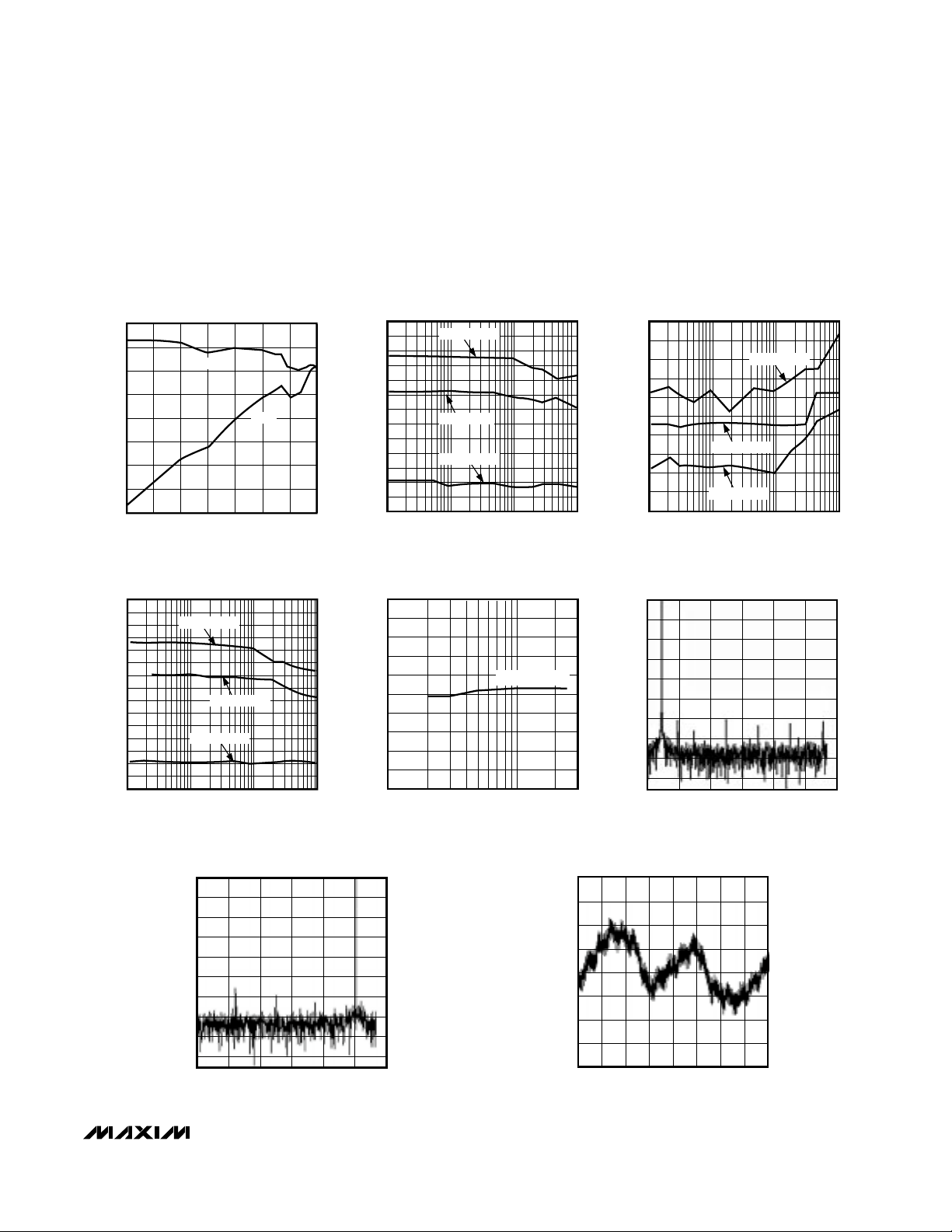
__________________________________________Typical Operating Characteristics
110
30
-70 -60 -40-50 -30 -20 -10 0
SINGLE-TONE SPURIOUS-FREE DYNAMIC
RANGE vs. INPUT AMPLITUDE (f
IN
= 100.1kHz)
MAX1201 toc01
INPUT AMPLITUDE (dBFS)
SFDR (dB)
60
50
40
90
100
80
70
dBFS
dBc
84
86
80
82
78
76
60
62
1k 10k 100k 1M
SIGNAL-TO-NOISE PLUS DISTORTION
vs. INPUT FREQUENCY
MAX1201 toc02
INPUT FREQUENCY (Hz)
SINAD (dB)
66
72
74
64
70
68
AIN = -0.5dBFS
AIN = -6dBFS
AIN = -20dBFS
-70
-72
-74
-90
1k 10k 100k 1M
TOTAL HARMONIC DISTORTION
vs. INPUT FREQUENCY
MAX1201 toc03
INPUT FREQUENCY (Hz)
THD (dB)
-82
-84
-78
-76
-88
-86
-80
AIN = -20dBFS
AIN = -6dBFS
AIN = -0.5dBFS
90
88
86
84
60
1k 10k 100k 1M
SIGNAL-TO-NOISE-RATIO
vs. INPUT FREQUENCY
MAX1201 toc04
INPUT FREQUENCY (Hz)
SNR (dB)
74
80
82
72
70
68
66
64
62
78
76
AIN = -0.5dBFS
AIN = -6dBFS
AIN = -20dBFS
90
88
84
86
70
100k 1M 3M
SIGNAL-TO-NOISE-RATIO PLUS DISTORTION
vs. SAMPLE RATE (f
IN
= 100.1kHz)
MAX1201 toc05
SAMPLE RATE (sps)
SINAD (dB)
74
80
82
72
78
76
AIN = -0.5dBFS
__________________________________________Typical Operating Characteristics
(AVDD= +5V, DVDD= DRVDD= +3.3V, V
RFPS
= +4.096V, V
RFNS
= AGND, f
CLK
= 4.5056MHz, differential input, VCM= +2.048V, cal-
ibrated, TA = +25°C, unless otherwise noted.)
-135
-105
-120
-90
-75
-60
-45
-30
-15
0
0 400k200k 600k 800k 1M 1.2M
TYPICAL FFT, fIN = 100.1kHz,
2048 VALUE RECORD
MAX1201 toc06
FREQUENCY (Hz)
AMPLITUDE (dBFS)
-135
-105
-120
-90
-75
-60
-45
-30
-15
0
0 400k200k 600k 800k 1M 1.2M
TYPICAL FFT, fIN = 1.0021MHz,
2048 VALUE RECORD
MAX1201 toc07
FREQUENCY (Hz)
AMPLITUDE (dBFS)
-2.0
-1.0
-0.5
-1.5
0.5
0
1.0
2.0
1.5
-8192 -4096-2048-6144 0 2048 4096 6144 8192
INTEGRAL NONLINEARITY vs.
TWO’S COMPLEMENT OUTPUT CODE
MAX1201 toc08
TWO’S COMPLEMENT OUTPUT CODE
INL (LSB)
Page 6

MAX1201
+5V Single-Supply, 2.2Msps, 14-Bit
Self-Calibrating ADC
6 _______________________________________________________________________________________
-1.0
-0.5
0
0.5
1.0
-8192 -4096 0-6144 2048-2048 4096 6144 8192
DIFFERENTIAL NONLINEARITY vs.
TWO’S COMPLEMENT OUTPUT CODE
MAX1201 toc9
TWO’S COMPLEMENT OUTPUT CODE
DNL (LSB)
14.0
13.5
13.0
10.0
1k 10k 100k 1M
EFFECTIVE NUMBER OF BITS
vs. INPUT FREQUENCY
MAX1201 toc10
INPUT FREQUENCY (Hz)
ENOB (BITS)
11.0
10.5
12.0
12.5
11.5
AIN = -0.5dBFS
AIN = -6dBFS
AIN = -20dBFS
Typical Operating Characteristics (continued)
(AVDD= +5V, DVDD= DRVDD= +3.3V, V
RFPS
= +4.096V, V
RFNS
= AGND, f
CLK
= 4.5056MHz, differential input, VCM= +2.048V, cal-
ibrated, TA = +25°C, unless otherwise noted.)
Pin Description
2, 4, 5
1
11
10
9
8
7
14
13
12
NAME FUNCTION
AGND Analog Ground
ST_CAL
Digital Input to Start Calibration.
ST_CAL = 0: Normal conversion mode.
ST_CAL = 1: Start self-calibration.
D10 Bit 10
D11 Bit 11
D12 Bit 12
D13 Bit 13 (MSB)
DOR Data Out-of-Range Bit
D7 Bit 7
D8 Bit 8
D9 Bit 9
3, 6 AV
DD
Analog Power Supply, +5V ±5%
PIN
17, 28
16
15
20
19
18
DGND Digital Ground
DRV
DD
Digital Power Supply for the Output Drivers. +3V to +5.25V, DRVDD≤ DVDD.
D6 Bit 6
D3 Bit 3
D4 Bit 4
D5 Bit 5
Page 7

MAX1201
+5V Single-Supply, 2.2Msps, 14-Bit
Self-Calibrating ADC
_______________________________________________________________________________________ 7
Pin Description (continued)
NAME FUNCTION
D2 Bit 2
TEST2
Test Pin 2. Leave unconnected.
TEST3
Test Pin 3. Leave unconnected.
D0 Bit 0 (LSB)
D1 Bit 1
TEST1
Test Pin 1. Leave unconnected.
DV
DD
Digital Power Supply, +3V to +5.25V.
CLK Input Clock. Receives power from AV
DD
to reduce jitter.
DAV
Data Valid Clock. Digital Output. This clock can be used to transfer the data to a memory or any
other data-acquisition system.
OE
Output Enable: Digital Input.
OE = 0: D0–D13 and DOR are high impedance.
OE = 1: All bits are active.
TEST0
Test Pin 0. Leave unconnected.
CM
Common-Mode Voltage. Analog Input. Drive midway between positive and negative reference
voltages.
RFPF Positive Reference Voltage. Force Input.
RFPS Positive Reference Voltage. Sense Input.
RFNF Negative Reference Voltage. Force Input.
PIN
21
25
24
23
22
26
27, 30
31
32
33
34
35
36
37
38
RFNS Negative Reference Voltage, Sense Input.
INP Positive Input Voltage
N.C. Not Connected. No internal connection.
39
40
41, 42
INN Negative Input Voltage
END_CAL
Digital Output for End of Calibration.
END_CAL = 0: Calibration in progress.
END_CAL = 1: Normal conversion mode.
43
44
Page 8

MAX1201
+5V Single-Supply, 2.2Msps, 14-Bit
Self-Calibrating ADC
8 _______________________________________________________________________________________
Detailed Description
Converter Operation
The MAX1201 is a 14-bit, monolithic, analog-to-digital
converter (ADC) capable of conversion rates up to
2.2Msps. It uses a multistage, fully differential, pipelined architecture with digital error correction and selfcalibration to provide 90dB (typ) spurious-free dynamic
range at a 2.2Msps sampling rate. Its signal-to-noise
ratio, harmonic distortion, and intermodulation products
are also consistent with 14-bit accuracy up to the
Nyquist frequency. This makes the device suitable for
applications such as xDSL, digital radio, instrumentation, and imaging.
Figure 1 shows the simplified, internal structure of the
ADC. A switched-capacitor pipelined architecture is
used to digitize the signal at a high throughput rate.
The first four stages of the pipeline use a low resolution
quantizer to approximate the input signal. The multiplying digital-to-analog converter (MDAC) stage is used to
subtract the quantized analog signal from the input.
The residue is then amplified with a fixed gain and
passed on to the next stage. The accuracy of the converter is improved by a digital calibration algorithm
which corrects for mismatches between the capacitors
in the switched capacitor MDAC. Note that the pipeline
introduces latency of four sampling periods between
the input being sampled and the output appearing at
D13–D0. While the device can handle both singleended or differential inputs (see
Requirements for
Reference and Analog Signal Inputs
), the latter mode of
operation will guarantee best THD and SFDR performance. The differential input provides the following
advantages compared to a single-ended operation:
• Twice as much signal input span
• Common-mode noise immunity
• Virtual elimination of the even-order harmonics
• Less stringent requirements on the input signal pro-
cessing amplifiers
Requirements for Reference
and Analog Signal Inputs
Fully differential switched capacitor circuits (SC) are
used for both the reference and analog inputs (Figure
2). This allows either single-ended or differential signals
to be used in the reference and/or analog signal paths.
The signal voltage on these pins (INP, INN, RFP_,
RFN_) should neither exceed the analog supply rail,
AVDDnor fall below ground.
STAGE1
7
DAV
INP
CM AV
DD
RFN_RFP_ AGND
INN
CLK
DV
DD
DGND
DRV
DD
ST_CAL
DOR
D13–D0
17
ADC
ADC MDAC
8X
S/H
STAGE2 STAGE3 STAGE4
CORRECTION AND
CALIBRATION LOGIC
END_CAL
OE
OUTPUT DRIVERS
CLOCK
GENERATOR
MAX1201
Figure 1. Internal Block Diagram
Page 9

MAX1201
+5V Single-Supply, 2.2Msps, 14-Bit
Self-Calibrating ADC
_______________________________________________________________________________________ 9
Choice of Reference
It is important to choose a low-noise reference, such as
the MAX6341, which can provide both excellent load
regulation and low temperature drift. The equivalent
input circuit for the reference pins is shown in Figure 3.
Note that the reference pins drive approximately 1kΩ of
resistance on chip. They also drive a switched capacitor
of 21pF. To meet the dynamic performance, the reference voltage is required to settle to 0.0015% within one
clock cycle. Carefully choose an appropriate driving circuit (Figure 4). The capacitors at the reference pins
(RFPF, RFNF) provide the dynamic charge required during each clock cycle, while the op amps ensure accuracy of the reference signals. These capacitors must have
low dielectric-absorption characteristics, such as polystyrene or teflon capacitors.
The reference pins can be connected to either singleended or differential voltages within the specified maximum levels. Typically, the positive reference pin (RFPF)
would be driven to 4.096V, and the negative reference
pin (RFNF) connected to analog ground. There are
sense pins, RFPS and RFNS, which can be used with
external amplifiers to compensate for any resistive drop
on these lines, internal or external to the chip. Assure a
correct reference voltage by using proper Kelvin connections at the sense pins.
Common-Mode Voltage
The switched capacitor circuit at the analog input allows
signals between AGND and the analog power supply.
Since the common-mode voltage has a strong influence
on the performance of the ADC, the best results are
obtained by choosing VCMto be at half the difference
between the reference voltages V
RFP
and V
RFN
. Achieve
this by using a resistive divider between the two reference potentials. Figure 4 shows the driving circuit for
good dynamic performance.
RFPF
INP
INN
RFPF
CM
CM
RFNF
Figure 2. Simplified MDAC Architecture
RFPF
RFPS
RFNF
RFNS
Figure 3. Equivalent Input at the Reference Pins. The sense
pins should not draw any DC current.
V
RFP
= 4.096V
V
RFN
= 0V
5k
5k
MAX410
CHIP BOUNDARY
CM
RFNS
RFNF
RFPS
RFPF
MAX410
MAX410
Figure 4. Drive Circuit for Reference Pins and Common-Mode
Pin
Page 10

MAX1201
+5V Single-Supply, 2.2Msps, 14-Bit
Self-Calibrating ADC
10 ______________________________________________________________________________________
Analog Signal Conditioning
For single-ended inputs, the negative analog input pin
(INN) is tied to the common-mode voltage pin (CM),
and the positive analog input pin (INP) is connected to
the input signal. The common-mode voltage of INP
must be equal to the common-mode input. To take full
advantage of the ADC’s superior AC performance up to
Nyquist frequency, drive the chip with differential signals. While in communication systems the signals may
inherently be available in differential mode, medical
and/or other applications may only provide singleended inputs. In this case, convert the single-ended
signals into differential ones by using the circuit recommended in Figure 5. Use low-noise, wideband amplifiers, such as the MAX4108, to maintain the signal
purity over the full-power bandwidth of the MAX1201.
Lowpass or bandpass filters may be required to
improve the signal-to-noise-and-distortion ratio of the
incoming signal. For low-frequency signals (<100kHz),
active filters may be used. For higher frequencies, passive filters are more convenient.
Single-Ended to Differential
Conversion Using Transformers
An alternative single-ended to differential-ended conversion method is a balun transformer such as the
CTX03-13675 from Coiltronics. An important benefit of
these transformers is their ability to level-shift a singleended signal, referred to ground on the primary side, to
optimum common-mode voltages on the secondary
side. At frequencies below 20kHz, the transformer core
begins to saturate, causing odd-order harmonics.
Clock Source Requirements
Pipelined ADCs typically need a 50% duty cycle clock.
To avoid this constraint, the MAX1201 provides a
divide-by-two circuit which relaxes this requirement.
The clock generator should be chosen commensurate
with the frequency range, amplitude and slew rate of
the signal source. If the slew rate of the input signal is
low, the jitter requirement on the clock is relaxed.
However, if the slew rate is high, the clock jitter needs
to be kept at a minimum. For a full-scale amplitude
input sine wave, the maximum possible SNR due completely to clock jitter is given by
For example, if fINis 1MHz and σ
JITTER
is 10ps RMS,
then the SNR limit due to jitter is approximately 84dB.
Generating such a clock source requires a low-noise
comparator and a low-phase noise signal generator. The
clock circuit shown in Figure 6 is a possible solution.
SNR
1
2
MAX
IN JITTER
f
=
⋅⋅ ⋅
πσ
MAX4108
INP
INN
CM
V-
V+
IN
CM
V+
V-
MAX4108
Figure 5. A simple circuit generates differential signals from a
single-ended input referred to analog ground. The commonmode voltage at INP and INN is the same as CM.
MAX961
CLK
V+
V+
0.1µF
0.1µF
0.1µF
1k
1k
CLK_IN
5k
Figure 6. Clock Generation Circuit Using Low-Noise Comparator
Page 11

MAX1201
+5V Single-Supply, 2.2Msps, 14-Bit
Self-Calibrating ADC
______________________________________________________________________________________ 11
Calibration Procedure
Since the MAX1201 is based on a pipelined architecture, low-resolution quantizers (“coarse ADCs”) are
used to approximate the input signal. MDACs of the
same resolution are then used to reconstruct the input
signal, which is subtracted from the input and the
residue is amplified by the switched-capacitor gain
stage. This residue is then passed on to the next stage.
The accuracy of the MAX1201 is limited by the precision of the MDAC, which is strongly dependent on the
matching of the capacitors used. The mismatch
between the capacitors is determined and stored in an
on-chip memory, which is later used during the conversion of the input signal.
During the calibration procedure, the clock must be
running continuously. ST_CAL (start of calibration) is
initiated by a positive pulse with a minimum width of
four clock cycles but no longer than about 17,400 clock
cycles (Figure 8).
The ST_CAL input may be asynchronous with the clock,
since it is retimed internally. With ST_CAL activated,
END_CAL goes low one or two clock cycles later and
remains low until the calibration is complete. During this
period, the reference voltages must be stable to less
than 0.01%; otherwise, the calibration will be invalid.
During calibration, the analog inputs INP and INN are
not used; however, better performance is achieved if
these inputs are static. Once END_CAL goes high (indicating that the calibration procedure is complete), the
ADC is ready for conversion.
Once calibrated, the MAX1201 is insensitive to small
changes (±5%) in power supply, voltage, or temperature. Following calibration, if the temperature changes
more than ±20°C, the device should be recalibrated to
maintain optimum performance.
Two’s Complement Output
The MAX1201 outputs data in two’s complement format. Table 1 shows how to convert the various fullscale inputs into their two’s complement output codes.
Applications Information
Signal-to-Noise Ratio (SNR)
For a waveform perfectly reconstructed from digital
samples, the theoretical maximum SNR is the ratio of
full-scale analog input (RMS value) to the RMS quantization error (residual error). The ideal, theoretical minimum analog-to-digital noise is caused by quantization
error only and results directly from the ADC’s resolution
(N bits):
SNR
(MAX)
= (6.02 · N + 1.76)dB
In reality, there are other noise sources besides quantization noise including thermal noise, reference noise,
clock jitter, etc. Therefore, SNR is computed by taking
the ratio of the RMS signal to the RMS noise which
includes all spectral components minus the fundamental, the first nine harmonics, and the DC offset.
t
S
tCHt
CL
N
CLK
AIN
SAMPLE
CLOCK
DAV
N-3 N-2 N-1 N N+1
D0–D13
N+1
N+2
N+3
N+4
N+5
t
OD
Figure 8. Timing for Start and End of Calibration
Figure 7. Main Timing Diagram
Z
Z = HIGH IMPEDANCE (THREE-STATED)
Z
DOR
D0–D13
OE
t
AC
t
REL
Figure 9. Timing for Bus Access and Bus Relinquish—
Controlled by Output Enable (OE)
CLK
ST_CAL
END_CAL
MIN 4 t
CLK
~17,400 CLK CYCLES
Page 12

MAX1201
+5V Single-Supply, 2.2Msps, 14-Bit
Self-Calibrating ADC
12 ______________________________________________________________________________________
Table 1. Binary Output Codes
Signal-to-Noise
Plus Distortion (SINAD)
SINAD is the ratio of the fundamental input frequency’s
RMS amplitude to all other ADC output signals.
SINAD (dB) = 20
· log [Signal
RMS
/ (Noise +
Distortion)
RMS
]
Effective Number of Bits (ENOB)
ENOB indicates the global accuracy of an ADC at a
specific input frequency and sampling rate. An ideal
ADC’s error consists only of quantization noise. With an
input range equal to the full-scale range of the ADC, the
effective number of bits can be calculated as follows:
ENOB = (SINAD - 1.76) / 6.02
Total Harmonic Distortion (THD)
THD is the ratio of the RMS sum of the first nine harmonics of the input signal to the fundamental itself. This
is expressed as:
where V1is the fundamental amplitude, and V2through
V9are the amplitudes of the 2nd through 9th-order harmonics.
Spurious-Free
Dynamic Range (SFDR)
SFDR is the ratio of RMS amplitude of the fundamental
(maximum signal component) to the RMS value of the
next largest spurious component, excluding DC offset.
Grounding and Power-Supply Decoupling
Grounding and power-supply decoupling strongly influence the performance of the MAX1201. At 14-bit resolution, unwanted digital crosstalk may couple through
the input, reference, power supply, and ground connections; this adversely affects the signal-to-noise ratio
or spurious-free dynamic range. In addition, electromagnetic interference (EMI) can either couple into or
be generated by the MAX1201. Therefore, grounding
and power-supply decoupling guidelines should be
closely followed.
First, a multilayer, printed circuit board (PCB) with separate ground and power-supply planes is recommended. Run high-speed signal traces on lines directly
above the ground plane. Since the MAX1201 has separate analog and digital ground buses (AGND and
DGND, respectively), the PCB should also have separate analog and digital ground sections connected at
only one point (star ground). Digital signals should run
above the digital ground plane and analog signals
should run above the analog ground plane. Digital signals should be kept far away from the sensitive analog
inputs, reference input senses, common-mode input,
and clock input.
THD 20 log
V
V
2
2
VV V
=
()
⋅
+++⋅⋅⋅+
324
2
9
2
1
SCALE OFFSET BINARY ONE’S COMPLEMENT TWO’S COMPLEMENT
+FSR - 1LSB 1111 .... 1111 0111 .... 1111 0111 .... 1111
+3/4FSR 1110 .... 0000 0110 .... 0000 0110 .... 0000
+1/2FSR 1100 .... 0000 0100 .... 0000 0100 .... 0000
+1/4FSR 1010 .... 0000 0010 .... 0000 0010 .... 0000
+0 1000 .... 0000 0000 .... 0000 0000 .... 0000
-0 —— .... —— 1111 .... 1111 —— .... ——
-1/4FSR 0110 .... 0000 1101 .... 1111 1110 .... 0000
-1/2FSR 0100 .... 0000 1011 .... 1111 1100 .... 0000
-3/4FSR 0010 .... 0000 1001 .... 1111 1010 .... 0000
-FSR +1LSB 0000 .... 0001 1000 .... 0000 1000 .... 0001
-FSR 0000 .... 0000 —— .... —— 1000 .... 0000
Page 13

MAX1201
+5V Single-Supply, 2.2Msps, 14-Bit
Self-Calibrating ADC
______________________________________________________________________________________ 13
The MAX1201 has three power-supply inputs: analog
VDD(AVDD), digital VDD(DVDD), and drive V
DD
(DRVDD). Each AVDDinput should be decoupled with
parallel ceramic chip capacitors of values 0.1µF and
0.001µF, with these capacitors as close to the pin as
possible and with the shortest possible connection to
the ground plane. The DVDDpins should also have
separate 0.1µF capacitors again adjacent to their
respective pins, as should the DRVDDpin. Minimize the
digital load capacitance. However, if the total load
capacitance on each digital output exceeds 20pF, the
DRVDDdecoupling capacitor should be increased or,
preferably, digital buffers should be added.
The power-supply voltages should also be decoupled
with large tantalum or electrolytic capacitors at the
point the voltages enter the PCB. Ferrite beads with
additional decoupling capacitors forming a pi network
could also improve performance.
The analog power-supply input (AVDD) for the
MAX1201 is typically +5V, while the digital supplies
can vary from +5V to +3V. Usually, DVDDand DRV
DD
pins are connected to the same power supply. Note
that the DVDDsupply voltage must be greater than or
equal to the DRVDDvoltage. For example, a digital
+3.3V supply could be connected to DRVDDwhile a
cleaner +5V supply is connected to DVDDresulting in
slightly improved performance. Alternatively, the +3.3V
supply could be connected to both DRVDDand DVDD.
However, the +3.3V supply should not be connected to
DVDDwhile the +5V supply is connected to DRV
DD
(Table 2).
Table 2. Power-Supply-Voltage
Combinations
Chip Information
TRANSISTOR COUNT: 56,577
SUBSTRATE CONNECTED TO AGND
AV
DD
(V)
DV
DD
(V)
DRV
DD
(V)
ALLOWED/
NOT ALLOWED
5 5 5 Allowed
5 5 3.3 Allowed
5 3.3 3.3 Allowed
5 3.3 5
Not
Allowed
Page 14

MAX1201
+5V Single-Supply, 2.2Msps, 14-Bit
Self-Calibrating ADC
14 ______________________________________________________________________________________
Package Information
MQFP44.EPS
Page 15

MAX1201
+5V Single-Supply, 2.2Msps, 14-Bit
Self-Calibrating ADC
______________________________________________________________________________________ 15
NOTES
Page 16

MAX1201
+5V Single-Supply, 2.2Msps, 14-Bit
Self Calibrating ADC
Maxim cannot assume responsibility for use of any circuitry other than circuitry entirely embodied in a Maxim product. No circuit patent licenses are
implied. Maxim reserves the right to change the circuitry and specifications without notice at any time.
16
____________________Maxim Integrated Products, 120 San Gabriel Drive, Sunnyvale, CA 94086 408-737-7600
© 1998 Maxim Integrated Products Printed USA is a registered trademark of Maxim Integrated Products.
NOTES
 Loading...