

Page 1
19-5554; Rev 0; 9/10
EVALUATION KIT
AVAILABLE
General Description
The MAX12005 satellite IF switch IC is designed for
multi-user applications supporting two quad universal
low-noise blocks (LNBs) to be matrix switched to four
satellite receivers. The system can be easily expanded
to accept 16 satellite IF inputs using the cascade option
and one additional satellite IF switch IC. A configuration
of eight satellite IF inputs to eight satellite receivers is
also possible by using two ICs and adding eight input
splitters. The insertion loss of these splitters can be compensated by a +6dB or +12dB input gain select.
There are two ways to control the switch function.
Each IC contains four DiSEqCK 2.0 decoders and four
alternate tone/voltage decoders. The decoders use an
integrated trimmed oscillator, simplifying the MAX12005
implementation into any system. There are four operational modes, which include LNB mode (for use within
the LNB), cascade master mode, cascade slave mode,
and single mode.
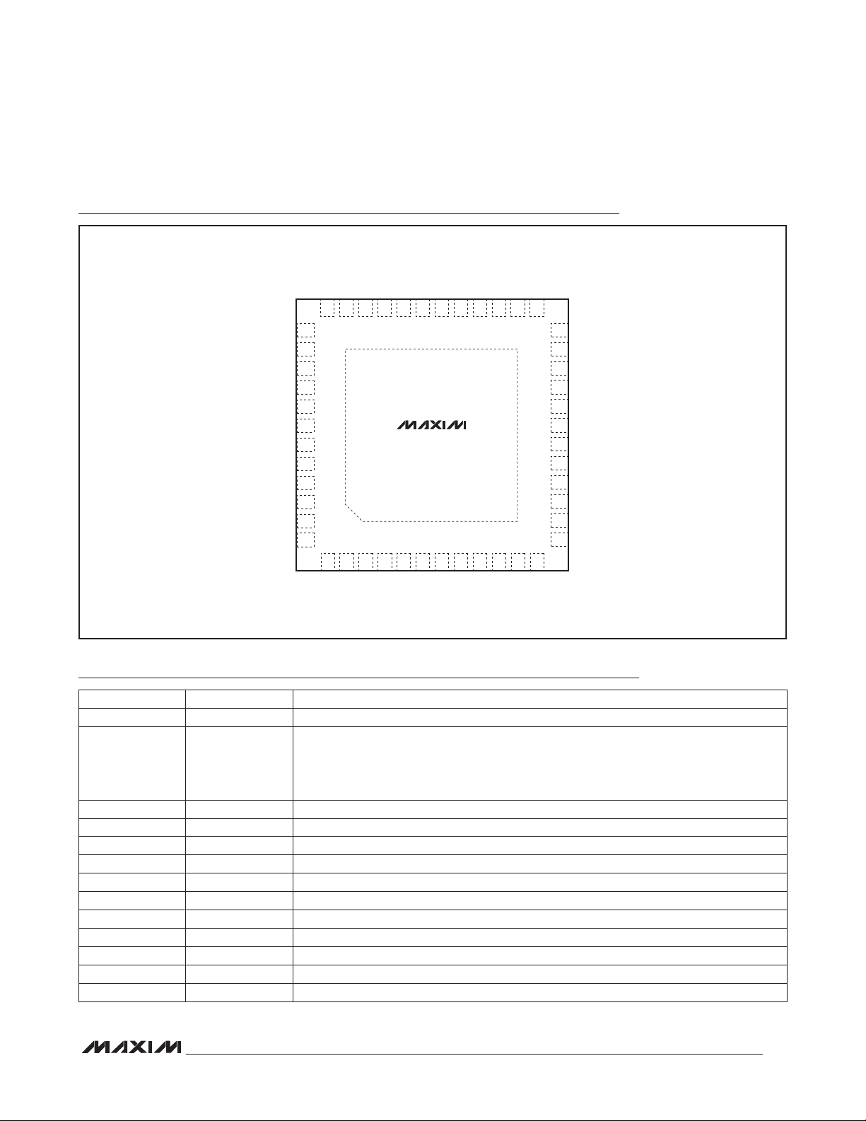
The satellite IF switch is designed on an advanced SiGe
process and is available in a lead-free 48-pin TQFN
surface-mount package (7mm x 7mm).
Satellite IF Switch
MAX12005
Features
S 8-Input-to-4-Output Matrix Switch
S Expandable to 16 Inputs with Cascade Master/
Slave Option
S 950MHz to 2150MHz Operation
S Greater than 30dB Switch Isolation
S 0/+6/+12dB Input Stage Gain Selection to
Compensate for Splitter Insertion Loss
Gain Step for All Input Stages Is Commonly
Controlled Through an Analog Select Pin
S Four Integrated DiSEqC 2.0 Decoders with
Integrated Oscillator
S Alternate Tone/Voltage Detection
S ESD Protected to 2kV HBM
Applications
Direct Broadcast Satellite Receivers
Satellite IF Distribution
L-Band Distribution
Ordering Information
PART TEMP RANGE PIN-PACKAGE
MAX12005ETM+ -40NC to +85NC 48 TQFN-EP*
+Denotes a lead(Pb)-free/RoHS-compliant package.
*EP = Exposed paddle.
DiSEqC is a trademark of EUTELSAT.
_______________________________________________________________ Maxim Integrated Products 1
For pricing, delivery, and ordering information, please contact Maxim Direct at 1-888-629-4642,
or visit Maxim’s website at www.maxim-ic.com.
Page 2
Satellite IF Switch
ABSOLUTE MAXIMUM RATINGS
VCC to GND ..........................................................-0.3V to +3.6V
RFIN1–RFIN8 to GND ...........................................-0.3V to +1.5V
CASCADE_IN1–CASCADE_IN4 to GND .............. -0.3V to +1.5V
RFOUT1–RFOUT4 to GND ....................... -0.3V to (V
DISEQC_TX1–DISEQC_TX4 to GND .........-0.3V to (V
DISEQC_RX1–DISEQC_RX4 to GND ........-0.3V to (V
+ 0.3V)
CC
CC
CC
+ 0.3V)
+ 0.3V)
GAIN_SELECT, MODE_SELECT
to GND ...................................................-0.3V to (V
MAX12005
Stresses beyond those listed under “Absolute Maximum Ratings” may cause permanent damage to the device. These are stress ratings only, and functional
operation of the device at these or any other conditions beyond those indicated in the operational sections of the specifications is not implied. Exposure to absolute
maximum rating conditions for extended periods may affect device reliability.
CAUTION! ESD SENSITIVE DEVICE
CC
+ 0.3V)
Continuous Power Dissipation (T
TQFN (derate 27.8 mW/NC above +70NC) ..................2.2W
Operating Ambient Temperature Range ........... -40NC to +85NC
Maximum Junction Temperature .....................................+150NC
Storage Temperature Range ............................ -65NC to +150NC
Lead Temperature (soldering, 10s) ................................+300NC
Soldering Temperature (reflow) ......................................+260NC
DC ELECTRICAL CHARACTERISTICS
(VCC = +3.0V to +3.5V, T
output loads = 75I. Typical values are at +3.3V and at T
PARAMETER SYMBOL CONDITIONS MIN TYP MAX UNITS
Supply Voltage V
Supply Current I
+12dB GAIN_SELECT Input HighLevel Voltage
+6dB GAIN_SELECT Input Voltage
Level and Range
0dB GAIN_SELECT Input Low-Level
Voltage
Single MODE_SELECT Input HighLevel Voltage
Master MODE_SELECT Input Voltage
Level and Range
Slave MODE_SELECT Input Voltage
Level and Range
LNB MODE_SELECT Input Low-Level
Voltage
GAIN_SELECT and MODE_SELECT
Input Current
DC Voltage Detect Input High Level V
DC Voltage Detect Input Low Level V
DISEQC_RX_ Input Current I
DISEQC_TX_ Output High-Level
Voltage
DISEQC_TX_ Output Low-Level
Voltage
= -40NC to +85NC, mode set to master, input gain stages set to highest gain, inputs matched to 75I,
A
CC
CC
V
IH
V
IN
V
IL
V
IH
V
IN
V
IN
V
IL
I
IN
IH
IL
IN
V
OH
V
OL
= +25NC, unless otherwise noted.) (Note 1)
A
3.0 3.5 V
VCC = 3.3V, 0dB, one input selected, four
outputs selected
VIN = V
CC
(Note 2) 1.23 V
(Note 2) 1.11 V
VIN = high or low 1
I
= -1mA
LOAD
I
= +1mA 0.4 V
LOAD
= +70NC)
A
VCC -
0.4V
1/2 V
CC
Q200mV
VCC -
0.4V
2/3 V
CC
Q200mV
1/3 V
CC
Q200mV
150 250 mA
0.4 V
0.4 V
10
-
V
CC
0.4V
V
mV
V
mV
mV
FA
FA
V
2
Page 3
Satellite IF Switch
AC ELECTRICAL CHARACTERISTICS
(MAX12005 EV Kit, VCC = +3.0V to +3.5V, f
set to 0dB, RF inputs matched to 75I, RF output loads = 75I. Typical values are at +3.3V and at T
noted.) (Note 1)
PARAMETER SYMBOL CONDITIONS MIN TYP MAX UNITS
Operation Frequency f
DISEQC_RX_ Tone Input Level V
Switch Gain at 950MHz (Note 3)
Cascade Input Switch Gain at
950MHz
Switch-to-Switch Gain Match D|S
Gain Slope with Frequency Between 950MHz and 2150MHz +3 dB
Single-Input Source Gain Change
3rd-Order Intermodulation Product
(Case 1)
= 950MHz, VIN = 70dBFV, T
IN
RF
fIN = 22kHz 60 mV
IN
0dB gain 0
+12dB gain +12
|S
21|
| At 950MHz (Note 4) -1.5 +3.5 dB
21
Gain change from single output connected to a single input to four outputs
connected to a single input
Output level set to +89dBFV by varying
IM3
three equal amplitude tones at 955MHz,
962MHz, and 965MHz; measure products
at 952MHz and 958MHz
= -40NC to +85NC, mode set to master, input gain stages
A
= +25NC, unless otherwise
A
950 2150 MHz
0 dB
-0.4 dB
-35 dBc
MAX12005
P-P
dB+6dB gain +6
Output level set to +89dBFV by varying
3rd-Order Intermodulation Product
(Case 2)
RFIN1–RFIN8 Input Return Loss |S
CASCADE_IN1–CASCADE_IN4 Input
Return Loss
RFOUT1–RFOUT4 Output Return Loss |S
Switch Isolation 55 dB
Port-to-Port Isolation 33 dB
DiSEqC Clock f
Note 1: Production tested at +25NC; guaranteed by design and characterization at -40NC and +85NC.
Note 2: To supply the specified input-voltage-detect levels requires the use of a voltage-divider comprised of 12.7kI and 1.02kI
Q0.5% tolerance resistors. The voltage being divided is expected to be V
Note 3: The common input gain step is set by analog control. All gain measurements have only one output connect to each input.
Switch gain measurements do not include cascade inputs as part of the switch signal path.
Note 4: Switch-to-switch gain match is defined as each switch to every other switch gain match. Each switch must be set up with
the same input gain step.
IM3
|S
OSC
three equal amplitude tones at 2135MHz,
2142MHz, and 2145MHz; measure prod-
ucts at 2132MHz and 2138MHz
| -12 dB
11
| -12 dB
11
| -12 dB
22
= 14.75V maximum and VOH = 16.75V minumum.
OL
-34 dBc
8 MHz
3
Page 4
Satellite IF Switch
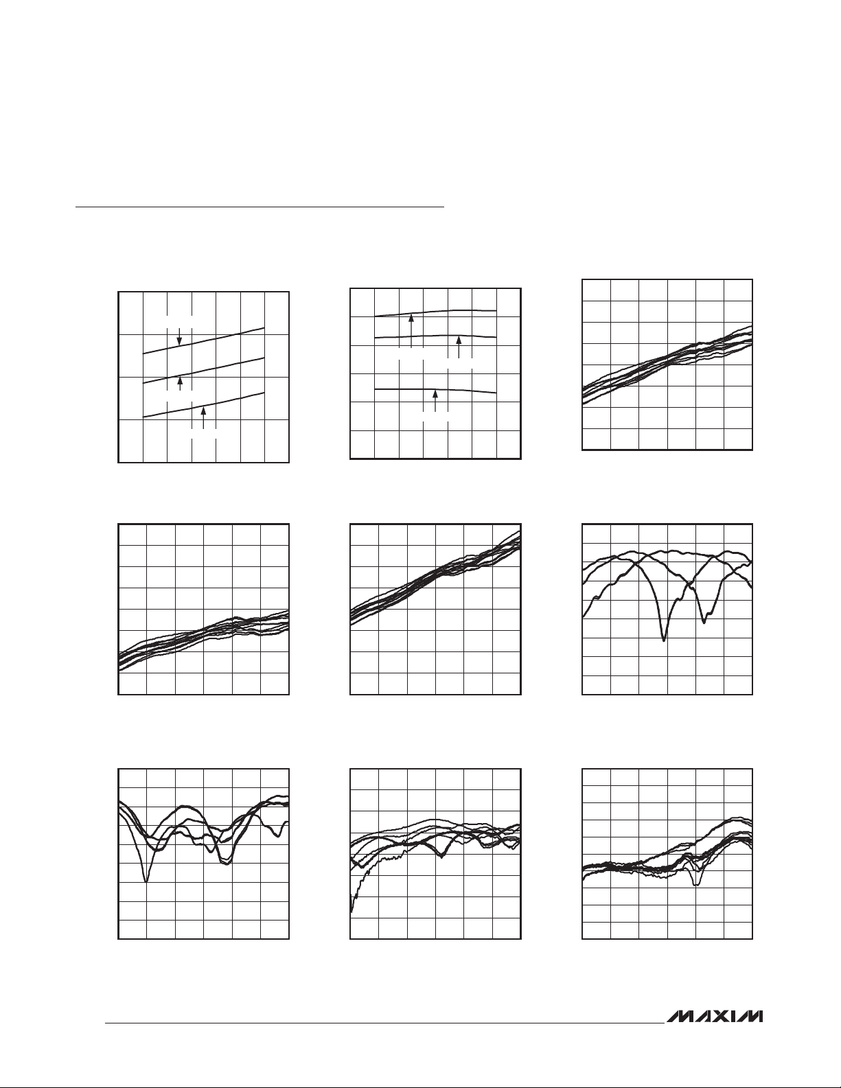
Typical Operating Characteristics
(MAX12005 EV Kit, VCC = +3.0V to +3.5V, fIN = 950MHz, VIN = 70dBFV, TA = -40NC to +85NC, mode set to master, input gain stages
set to 0dB, RF inputs matched to 75I, RF output loads = 75I. Typical values are at +3.3V and at T
Production tested at +25NC; guaranteed by design and characterization at -40NC and +85NC.)
VOLTAGE vs. CURRENT (0dB GAIN)
200
MAX12005
180
160
CURRENT (mA)
140
120
2.9 3.6
TA = +85°C
TA = +25°C
TA = -40°C
VOLTAGE (V)
S21 +85°C (0dB GAIN, VAR. IN/OUT)
4
3
2
1
0
-1
MAGNITUDE (dB)
-2
-3
-4
MAX12005 toc01
-1
GAIN (dB)
-2
-3
-4
3.53.43.33.23.13.0
MAX12005 toc04
-1
MAGNITUDE (dB)
-2
-3
-4
VOLTAGE vs. GAIN (+25°C)
2
1
0
2.9 3.6
2150MHz
VOLTAGE (V)
1550MHz
950MHz
3.53.43.33.23.13.0
S21 -40°C (0dB GAIN, VAR. IN/OUT)
4
3
2
1
0
MAX12005 toc02
MAX12005 toc05
= +25NC, unless otherwise noted.
A
S21 +25°C (0dB GAIN, VAR. IN/OUT)
4
3
2
1
0
-1
MAGNITUDE (dB)
-2
-3
-4
9.5E+08
1.15E+09
FREQUENCY (Hz)
1.35E+09
1.55E+09
RF S11 (VAR. INPUT)
-5
-10
-15
-20
-25
-30
MAGNITUDE (dB)
-35
-40
-45
-50
1.75E+09
1.95E+09
MAX12005 toc03
2.15E+09
MAX12005 toc06
-5
-10
-15
-20
-25
-30
MAGNITUDE (dB)
-35
-40
-45
-50
4
9.5E+08
1.15E+09
FREQUENCY (Hz)
1.35E+09
RF S22 (VAR. OUTPUT)
9.5E+08
1.15E+09
FREQUENCY (Hz)
1.35E+09
1.55E+09
1.55E+09
1.75E+09
1.75E+09
1.95E+09
1.95E+09
2.15E+09
MAX12005 toc07
2.15E+09
9.5E+08
-10
-20
-30
-40
-50
ISOLATION (dB)
-60
-70
-80
-90
9.5E+08
1.15E+09
FREQUENCY (Hz)
1.35E+09
1.55E+09
1.75E+09
SWITCH ISOLATION (VAR. CH)
1.15E+09
FREQUENCY (Hz)
1.35E+09
1.55E+09
1.75E+09
1.95E+09
1.95E+09
2.15E+09
MAX12005 toc08
2.15E+09
9.5E+08
1.15E+09
FREQUENCY (Hz)
1.35E+09
1.55E+09
PORT-TO-PORT ISOLATION (VAR. PORTS)
-30
-35
-40
-45
-50
-55
ISOLATION
-60
-65
-70
-75
-80
9.5E+08
1.15E+09
1.35E+09
1.55E+09
FREQUENCY (Hz)
1.75E+09
1.75E+09
1.95E+09
1.95E+09
2.15E+09
MAX12005 toc09
2.15E+09
Page 5
Satellite IF Switch
Pin Configuration
MAX12005
TOP VIEW
RFOUT3
GND
V
RFOUT2
GND
V
RFOUT1
GND
V
V
MODE_SELECT
GAIN_SELECT
CC
CC
CC
CC
CC
GND
V
35
34 33 32 31 30 29 28 27
36
37
38
39
40
41
42
43
44
45
46
+
47
48
2
3 4 5 6 7 8 9 10
1
GND
RFIN2
RFIN1
VCCRFOUT4
GND
DISEQC_TX1
DISEQC_RX1
MAX12005
GND
RFIN3
DISEQC_TX2
DISEQC_RX2
GND
RFIN4
DISEQC_RX3
RFIN5
DISEQC_RX4
DISEQC_TX3
25
26
12
11
GND
RFIN6
DISEQC_TX4
GND
24
CASCADE_IN4
23
22
GND
21
CASCADE_IN3
GND
20
CASCADE_IN2
19
18
GND
17
CASCADE_IN1
16
GND
RFIN8
15
GND
14
13
RFIN7
GND
TQFN
Pin Description
PIN NAME FUNCTION
1 RFIN1 RF Input from LNB
2, 4, 6, 8, 10, 12,
14, 16, 18, 20,
22, 24, 35, 38,
GND Electrical Ground
41, 44
3 RFIN2 RF Input from LNB
5 RFIN3 RF Input from LNB
7 RFIN4 RF Input from LNB
9 RFIN5 RF Input from LNB
11 RFIN6 RF Input from LNB
13 RFIN7 RF Input from LNB
15 RFIN8 RF Input from LNB
17 CASCADE_IN1 Cascade Input from RF Output of Second MAX12005 in Slave Mode
19 CASCADE_IN2 Cascade Input from RF Output of Second MAX12005 in Slave Mode
21 CASCADE_IN3 Cascade Input from RF Output of Second MAX12005 in Slave Mode
23 CASCADE_IN4 Cascade Input from RF Output of Second MAX12005 in Slave Mode
5
Page 6

Satellite IF Switch
Pin Description (continued)
PIN NAME FUNCTION
25 DISEQC_TX4
26 DISEQC_RX4 Input for DiSEqC Slave Signal from Satellite Receiver or Master
27 DISEQC _TX3
MAX12005
28 DISEQC _RX3 Input for DiSEqC Slave Signal from Satellite Receiver or Master
29 DISEQC _TX2
30 DISEQC _RX2 Input for DiSEqC Slave Signal from Satellite Receiver or Master
31 DISEQC _TX1
32 DISEQC _RX1 Input for DiSEqC Slave Signal from Satellite Receiver or Master
33, 36, 39, 42,
45, 46
34 RFOUT4 RF Output to Satellite Receiver
37 RFOUT3 RF Output to Satellite Receiver
40 RFOUT2 RF Output to Satellite Receiver
43 RFOUT1 RF Output to Satellite Receiver
47 MODE_SELECT Satellite Switch Mode Select
48 GAIN_SELECT Gain Select for All Input Stages
— EP
V
CC
Return DiSEqC Signal Output to Satellite Receiver (Master) or Outputs Envelope of
Received DiSEqC Signal for Use by External Controller
Return DiSEqC Signal Output to Satellite Receiver (Master) or Outputs Envelope of
Received DiSEqC Signal for Use by External Controller
Return DiSEqC Signal Output to Satellite Receiver (Master) or Outputs Envelope of
Received DiSEqC Signal for Use by External Controller
Return DiSEqC Signal Output to Satellite Receiver (Master) or Outputs Envelope of
Received DiSEqC Signal for Use by External Controller
3.0V to 3.5V Supply. Analog supply pins 33, 36, 39, and 42. Digital supply pins 45 and
46.
Exposed Pad Ground. The exposed pad must be soldered to the circuit board for proper thermal and electrical performance.
6
Page 7

Satellite IF Switch
Functional Diagram
33, 36, 39, 42, 45
V
0/+6/+12dB
RFIN1
1
3
RFIN2
RFIN3
5
9:1 MUX
SATELLITE IF SWITCH
9:1 MUX
CC
43
RFOUT1
40
RFOUT2
MAX12005
RFOUT4
V
37
34
46
CC
47
48
16
GND
7
RFIN4
RFIN5
9
RFIN6
11
13
RFIN7
15
RFIN8
CASCADE_IN1
CASCADE_IN2
9:1 MUX
9:1 MUX
CASCADE_IN3
CASCADE_IN4
MAX12005
PORT SWITCH CONTROL
DETECTOR
DiSEqC 2.0
VOLTAGE/ TONE
DISEQC_TX1
DISEQC_RX1
3117 19 21 23 32 29 30 27 28
DISEQC_TX2
DiSEqC 2.0
DISEQC_RX2
DETECTOR
DiSEqC 2.0
VOLTAGE/ TONE
DISEQC_TX3
CONTROL
DETECTOR
VOLTAGE/ TONE
DISEQC_RX3
LOGIC
DiSEqC 2.0
DISEQC_TX4
25 26
DETECTOR
VOLTAGE/ TONE
FREQUENCY
DISEQC_RX4
2, 4, 6, 8, 10, 12, 14, 18,
20, 22, 24, 35, 38, 41, 44
RFOUT3
MODE_SELECT
GAIN_SELECT
8MHz
OSCILLATOR
OUT
GND
7
Page 8

Satellite IF Switch
The MAX12005 satellite IF switch features eight 75I
inputs with three selectable gain steps of 0, +6dB, and
+12dB. Each of the eight input amplifiers feeds into four
nine-to-one multiplexers with the switching controlled
by voltage/tone or DiSEqC signaling from up to four
receivers. The output of each multiplexer is then sent to
a satellite receiver through a 75I buffered output stage.
The satellite IF switch has four modes of operation. Two
MAX12005
modes are used to increase the number of IF inputs by
cascading two MAX12005 ICs together. The first IC is
set to master mode to enable the four cascade inputs.
The second IC is set to slave mode with its outputs
connected to the cascade inputs of the master IC.
The LNB mode sets up the IC to recognize LNB DiSEqC
signaling to control switching and ignore DiSEqC
signaling for multiswitch applications. The single mode
sets up the IC to recognize multiswitch DiSEqC signaling
to control switching and ignore LNB DiSEqC signaling.
For the LNB, single, and slave modes, the four cascade
inputs are disabled.
Detailed Description
Input Gain Select
The voltage supplied to the GAIN_SELECT pin provides
the selection for one of three gain settings available at all
eight input stages, as follows:
GND = 0dB
1/2 VCC = +6dB
V
The +6dB gain step voltage can be set through the
use of a simple supply voltage-divider. This gain select
feature is intended to compensate for input signal losses
due to the use of input RF signal splitters.
= +12dB
CC
Chip Mode Select
The voltage supplied to the MODE_SELECT pin provides
the selection for one of four IC operational modes, as
follows:
GND = LNB Mode
1/3 V
2/3 V
V
The slave mode and master mode voltages can be set
through the use of simple supply voltage-dividers.
= Slave Mode (Cascade Operation)
CC
= Master Mode (Cascade Operation)
CC
= Single Mode
CC
Switch Control
Voltage/tone signaling is the default switch control after
power-up or when a receiver is connected or reconnected with the die power on. After an individual decoder
receives a DiSEqC signal, that decoder switches from
voltage/one control to DiSEqC control until a new receiver
connection is made or when the IC has a power-on reset.
Layout Considerations
To minimize coupling between different sections of the
IC, a star power-supply routing configuration with a large
decoupling capacitor at a central V
mended. The V
each going to a separate V
a bypass capacitor as close as possible to each supply pin. This arrangement provides local decoupling at
each V
for a low-inductance ground connection. Do not share
the capacitor ground vias with any other branch. The
MAX12005 EV kit can be used as a starting point for
layout. For best performance, take into consideration
grounding and routing of RF, baseband, and powersupply PCB proper line. Make connections from vias
to the ground plane as short as possible. On the highimpedance ports, keep traces short to minimize shunt
capacitance. EV kit schematic and Gerber files can be
found at www.maxim-ic.com.
pin. Use at least one via per bypass capacitor
CC
traces branch out from this node,
CC
node in the circuit. Place
CC
node is recom-
CC
SPI is a trademark of Motorola, Inc.
8
Page 9

Satellite IF Switch
DiSEqC Slave Control Interface
The DiSEqC interface is designed according to the
DiSEqC Bus Functional Specification version 4.2. All
framing bytes 0xE0 through 0xE7 are supported. The
following address bytes are supported:
PRIMARY DEVICE
TO SAT RECEIVER 1
TO SAT RECEIVER 2
TO SAT RECEIVER 3
TO SAT RECEIVER 4
RFOUT1
RFOUT2
RFOUT3
RFOUT4
CASCADE3
CASCADE4
CASCADE1
CASCADE2
0x00 Any device
0x10 Any LNB, switcher, or SMATV
0x11 LNB
0x14 Switcher, DC-blocking
RFIN1
RFIN2
RFIN3
RFIN4
RFIN5
RFIN6
RFIN7
RFIN8
SAT A, LOW, VERTICAL
SAT A, LOW, HORIZONTAL
SAT A, HIGH, VERTICAL
SAT A, HIGH, HORIZONTAL
SAT B, LOW, VERTICAL
SAT B, LOW, HORIZONTAL
SAT B, HIGH, VERTICAL
SAT B, HIGH, HORIZONTAL
MAX12005
SECONDARY DEVICE
RFOUT1
RFOUT2
RFOUT3
RFOUT4
CASCADE3
CASCADE4
Figure 1. Typical Cascade Connection Between Two Satellite Switch ICs
CASCADE1
CASCADE2
RFIN1
RFIN2
RFIN3
RFIN4
RFIN5
RFIN6
RFIN7
RFIN8
SAT C, LOW, VERTICAL
SAT C, LOW, HORIZONTAL
SAT C, HIGH, VERTICAL
SAT C, HIGH, HORIZONTAL
SAT D, LOW, VERTICAL
SAT D, LOW, HORIZONTAL
SAT D, HIGH, VERTICAL
SAT D, HIGH, HORIZONTAL
9
Page 10
Satellite IF Switch
Table 1 shows the coherence between the terms used
by the DiSEqC standard and the pin names used by the
MAX12005 along with the command sequences used to
control switching.
Table 2 lists the supported command bytes. The command byte is the 3.byte in the DiSEqC master frame
(refer to the DiSEqC Bus Functional Specification version 4.2, top of page 13). The DiSEqC slave only sends
MAX12005
Table 1. DiSEqC Slave Control Interface
DEVICE
(Note 1)
Primary RFIN1 Satellite A, low band, vertical polarization 0x23, 0x22, 0x20, 0x21
Secondary RFIN1 Satellite C, low band, vertical polarization 0x27, 0x22, 0x20, 0x21
Note 1: The primary device outputs connect directly to the satellite receivers. The secondary device outputs connect to the primary
device through the cascade inputs. Also see Figure 1.
Note 2: Only those DiSEqC commands that differ between sequences have to be sent to change the input, not all four commands.
By default RFIN1 from the primary device is selected.
The DiSEqC interface is designed according to the DiSEqC Bus Functional Specification version 4.2.
INPUT SIGNAL FROM
RFIN2 Satellite A, low band, horizontal polarization 0x23, 0x22, 0x20, 0x25
RFIN3 Satellite A, high band, vertical polarization 0x23, 0x22, 0x24, 0x21
RFIN4 Satellite A, high band, horizontal polarization 0x23, 0x22, 0x24, 0x25
RFIN5 Satellite B, low band, vertical polarization 0x23, 0x26, 0x20, 0x21
RFIN6 Satellite B, low band, horizontal polarization 0x23, 0x26, 0x20, 0x25
RFIN7 Satellite B, high band, vertical polarization 0x23, 0x26, 0x24, 0x21
RFIN8 Satellite B, high band, horizontal polarization 0x23, 0x26, 0x24, 0x25
RFIN2 Satellite C, low band, horizontal polarization 0x27, 0x22, 0x20, 0x25
RFIN3 Satellite C, high band, vertical polarization 0x27, 0x22, 0x24, 0x21
RFIN4 Satellite C, high band, horizontal polarization 0x27, 0x22, 0x24, 0x25
RFIN5 Satellite D, low band, vertical polarization 0x27, 0x26, 0x20, 0x21
RFIN6 Satellite D, low band, horizontal polarization 0x27, 0x26, 0x20, 0x25
RFIN7 Satellite D, high band, vertical polarization 0x27, 0x26, 0x24, 0x21
RFIN8 Satellite D, high band, horizontal polarization 0x27, 0x26, 0x24, 0x25
a reply if requested by a framing byte 0xE2 or 0xE3
in the master frame (refer to DiSEqC Bus Functional
Specification version 4.2, bottom of page 13). All DiSEqC
commands control the contents of the DiSEqC registers
described in chapter 7.1.
Table 3 lists the supported command bytes. The DiSEqC
commands are internally mapped to individually named
registers. The registers do not have an address.
DiSEqC COMMAND SEQUENCE
(Note 2)
10
Page 11

Satellite IF Switch
Table 2. DiSEqC Slave Control Interface Command Bytes
HEX VALUE COMMAND FUNCTION DATA BYTES SLAVE REPLY
0x00 Reset Reset DiSEqC decoder — Framing byte
0x01 Clr Reset
0x04 Set Contend
0x05 Contend
0x06 Clr Contend
0x07 Address
0x08 Move C
0x09 Move
0x10 Status
0x11 Config
0x14 Switch 0
0x20 Set Lo
0x21 Set VR
0x22 Set Pos A
0x23 Set S0A
0x24 Set Hi
0x25 Set HL
0x26 Set Pos B
0x27 Set S0B
0x30 Sleep
0x31 Awake
Clear reset flag
Clears Status_reg, bit 0
Set contention flag
Sets Status_reg, bit 7
Return address only if contention flag is set
Reads Address_reg
Clear contention flag
Clears Status_reg, bit 7
Return address unless contention flag is set
Reads Address_reg
Change address only if contention flag is set
Writes to Address_reg
Change address unless contention flag is set
Writes to Address_reg
Read status register flags
Reads Status_reg
Read configuration flags
Reads Configuration_reg
Read switching state flags
Reads Switch_reg
Select the low local oscillator frequency
Clears Switch_reg, bit 4
Select vertical polarization (or right circular)
Clears Switch_reg, bit 5
Select satellite position A (or position C)
Clears Switch_reg, bit 6
Select switch option A (i.e. positions A/B)
Clears Switch_reg, bit 7
Select the high local oscillator frequency
Sets Switch_reg, bit 4
Select horizontal polarization (or left circular)
Sets Switch_reg, bit 5
Select satellite position B (or position D)
Sets Switch_reg, bit 6
Select switch option B (i.e. positions C/D)
Sets Switch_reg, bit 7
Ignore all bus commands except Awake
Sets Status_reg, bit 1
Respond to future bus commands normally
Clears Status_reg, bit 1
— Framing byte
— Framing byte
—
— Framing byte
—
1 byte Framing byte
1 byte Framing byte
—
—
—
— Framing byte
— Framing byte
— Framing byte
— Framing byte
— Framing byte
— Framing byte
— Framing byte
— Framing byte
— Framing byte
— Framing byte
Framing + data
byte
Framing + data
byte
Framing + data
byte
Framing + data
byte
Framing + data
byte
MAX12005
11
Page 12

Satellite IF Switch
Table 2. DiSEqC Slave Control Interface Command Bytes (continued)
HEX VALUE COMMAND FUNCTION DATA BYTES SLAVE REPLY
0x38 Write N0
0x50 LO string
Write to port group 0
Controls Switch_reg, bits 7 downto 4 (Note 1)
Read current frequency
Reads Low_LOF_reg2/1 or High_LOF_reg2/1
depending on Switch_reg, bit 4 (Note 2)
1 byte Framing byte
—
Framing + 2 data
bytes
MAX12005
0x51 LO now
0x52 LO Lo
0x53 LO Hi
Note 1: Refer to DiSEqC Bus Functional Specification version 4.2, page 18.
Note 2: Refer to DiSEqC Bus Functional Specification version 4.2, page 22.
Read current frequency table entry number
Reads Low_LOF_reg0, bit 3 downto 0 or
High_LOF_reg0, bit 3 downto 0
depending on Switch_reg, bit 4
Read low-frequency table entry number
Reads Low_LOF_reg0, bit 3 downto 0
Read high-frequency table entry number
Reads High_LOF_reg0, bit 3 downto 0
Table 3. DiSEqC Slave Control Interface Registers
ADDRESS BIT ACC NAME FUNCTION DEFAULT
Address_reg 7:0 RW address DiSEqC address
7 RW contention Bus contention flag 0
6 R standby Standby mode 0
5 — Unused — —
4 R aux_power Auxiliary power available 0
Status_reg
Configuration_reg
3 — Unused — —
2 RW voltage 0 = Low DC, 1 = High DC
1 RW sleep 0 = Awake, 1 = Sleep 0
0 RW reset Reset flag 1
7 R analog Analog output facility 0
6 R standby Standby facility 0
5 R positioner Positioner capability 0
4 R power_detection External power-detection capability 0
3 R loop_through Loopthrough facility 0
2 R polarizer Polarizer capability 0
1 R switch Switcher capability 1
0 R lof_values LOF value output capability 1
—
—
—
Framing + data
byte
Framing + data
byte
Framing + data
byte
LNB: 0x11
Switch: 0x14
Depends on
voltage input
12
Page 13

Satellite IF Switch
Table 3. DiSEqC Slave Control Interface Registers (continued)
ADDRESS BIT ACC NAME FUNCTION DEFAULT
7 RW option 0 = Positions A/B, 1 = Positions C/D 0
6 RW satellite 0 = Satellite A(C), 1 = Satellite B(D) 0
5 RW polarization 0 = Vertical, 1 = Horizontal 0
4 RW band 0 = Low band, 1 = High band 0
Switch_reg
Low_LOF_reg_2
Low_LOF_reg_1
Low_LOF_reg_0
High_LOF_reg_2
High_LOF_reg_1
High_LOF_reg_0
3 RW option_switchable Options switch available
2 R satellite_switchable Satellite switch available 1
1 R polarization_switchable Polarization switch available 1
0 R band_switchable Band switch available 1
7:4 R low_10GHz Low LOF value, 10GHz digit 0000
3:0 R low_1GHz 1GHz digit 1001
7:4 R low_100MHz 100MHz digit 0111
3:0 R low_10MHz 10MHz digit 0101
7:4 R low_1MHz 1MHz digit 0000
3:0 R low_table_entry Table entry number 0010
7:4 R high_10GHz High LOF value, 10GHz digit 0001
3:0 R high_1GHz 1GHz digit 0000
7:4 R high_100MHz 100MHz digit 0110
3:0 R high_10MHz 10MHz digit 0000
7:4 R high_1MHz 1MHz digit 0000
3:0 R high_table_entry Table entry number 0100
MAX12005
Depends on
cascade input
Chip Information
PROCESS: BiCMOS
Package Information
For the latest package outline information and land patterns,
go to www.maxim-ic.com/packages. Note that a “+”, “#”, or
“-” in the package code indicates RoHS status only. Package
drawings may show a different suffix character, but the drawing
pertains to the package regardless of RoHS status.
PACKAGE
TYPE
48 TQFN T4877+4
PACKAGE
CODE
OUTLINE
NO.
21-0144 90-0130
LAND
PATTERN NO.
13
Page 14

Satellite IF Switch
Revision History
REVISION
NUMBER
0 9/10 Initial release —
REVISION
DATE
MAX12005
DESCRIPTION
PAGES
CHANGED
Maxim cannot assume responsibility for use of any circuitry other than circuitry entirely embodied in a Maxim product. No circuit patent licenses are implied.
Maxim reserves the right to change the circuitry and specifications without notice at any time.
14 Maxim Integrated Products, 120 San Gabriel Drive, Sunnyvale, CA 94086 408-737-7600
©
2010 Maxim Integrated Products Maxim is a registered trademark of Maxim Integrated Products, Inc.
 Loading...