

Page 1
MAX1179/MAX1187/MAX1189
16-Bit, 135ksps, Single-Supply ADCs with
Bipolar Analog Input Range
________________________________________________________________ Maxim Integrated Products 1
19-2675; Rev 1; 1/03
For pricing, delivery, and ordering information, please contact Maxim/Dallas Direct! at
1-888-629-4642, or visit Maxim’s website at www.maxim-ic.com.
General Description
The MAX1179/MAX1187/MAX1189 16-bit, low-power,
successive-approximation analog-to-digital converters
(ADCs) feature automatic power-down, a factorytrimmed internal clock, and a 16-bit wide parallel interface. The devices operate from a single +4.75V to
+5.25V analog supply and feature a separate digital
supply input for direct interface with +2.7V to +5.25V
digital logic.
The MAX1179 accepts a bipolar input voltage range of
±5V. The MAX1187 accepts an analog input voltage
range from 0 to +10V, while the MAX1189 accepts a
bipolar analog input voltage range of ±10V. All devices
consume only 23mW at a sampling rate of 135ksps
when using an external reference and 29mW when
using the internal +4.096V reference. AutoShutdown™
reduces supply current to 0.4mA at 10ksps. The
MAX1179/MAX1187/MAX1189 are ideal for high-performance, battery-powered data-acquisition applications.
Excellent AC performance (THD = -100dB) and DC
accuracy (±2LSB INL) make the MAX1179/MAX1187/
MAX1189 ideal for industrial process control, instrumentation, and medical applications.
The MAX1179/MAX1187/MAX1189 are available in a
28-pin TSSOP package and are fully specified over the
-40°C to +85°C extended temperature range and the
0°C to +70°C commercial temperature range.
Applications
Temperature Sensing and Monitoring
Industrial Process Control
I/O Modules
Data-Acquisition Systems
Precision Instrumentation
Features
♦ Analog Input Voltage Range: ±10V, ±5V, or 0 to 10V
♦ 16-Bit Wide Parallel Interface
♦ Single +4.75V to +5.25V Analog Supply Voltage
♦ Interfaces with +2.7V to +5.25V Digital Logic
♦ ±2LSB INL (max)
♦ ±1LSB DNL (max)
♦ Low Supply Current (MAX1189)
5.3mA (External Reference)
6.2mA (Internal Reference)
5µA AutoShutdown Mode
♦ Small Footprint
28-Pin TSSOP Package
Ordering Information
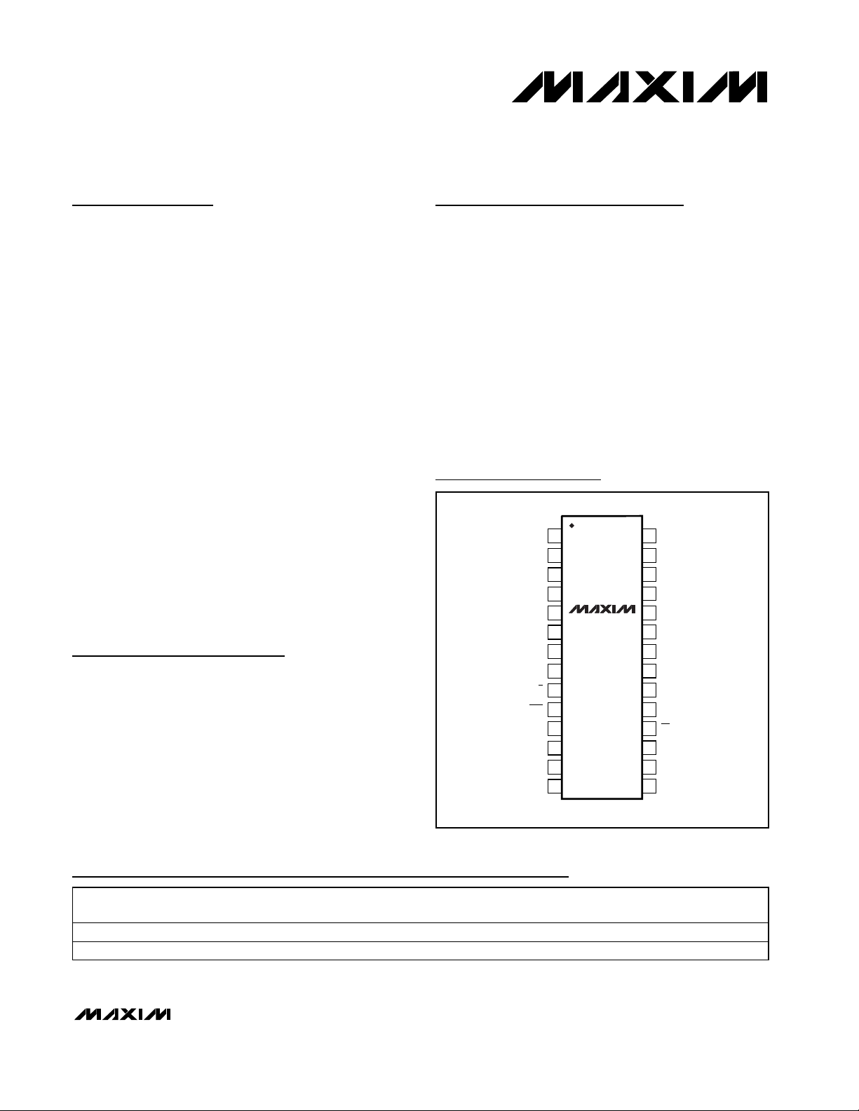
Pin Configuration
AutoShutdown is a trademark of Maxim Integrated Products, Inc.
Ordering Information continued at end of data sheet.
TOP VIEW
D10
D11
D12
D13
D14
D15
R/C
EOC
AV
AGND
AIN
AGND
1
D8
2
D9
3
4
5
MAX1179
6
MAX1187
MAX1189
7
8
9
10
11
DD
12
13
14
28
27
26
25
24
23
22
21
20
19
18
17
16
15
D7
D6
D5
D4
D3
D2
D1
D0
DV
DD
DGND
CS
RESET
REF
REFADJ
TSSOP
PART TEMP RANGE PIN-PACKAGE
MAX1179ACUI 0°C to +70°C 28 TSSOP ±5V ±2
MAX1179BCUI 0°C to +70°C 28 TSSOP ±5V ±2
INPUT VOLTAGE
RANGE
INL (LSB)
Page 2
MAX1179/MAX1187/MAX1189
16-Bit, 135ksps, Single-Supply ADCs with
Bipolar Analog Input Range
2 _______________________________________________________________________________________
ABSOLUTE MAXIMUM RATINGS
Stresses beyond those listed under “Absolute Maximum Ratings” may cause permanent damage to the device. These are stress ratings only, and functional
operation of the device at these or any other conditions beyond those indicated in the operational sections of the specifications is not implied. Exposure to
absolute maximum rating conditions for extended periods may affect device reliability.
AVDDto AGND .........................................................-0.3V to +6V
DV
DD
to DGND.........................................................-0.3V to +6V
AGND to DGND.....................................................-0.3V to +0.3V
AIN to AGND .....................................................-16.5V to +16.5V
REF, REFADJ to AGND............................-0.3V to (AV
DD
+ 0.3V)
CS, R/C, RESET to DGND ........................................-0.3V to +6V
D_, EOC to DGND ...................................-0.3V to (DV
DD
+ 0.3V)
Maximum Continuous Current Into Any Pin ........................50mA
Continuous Power Dissipation (T
A
= +70°C)
28-Pin TSSOP (derate 12.8mW/°C above +70°C) .....1026mW
Operating Temperature Range
MAX11_ _ _CUI...................................................0°C to +70°C
MAX11_ _ _EUI ................................................-40°C to +85°C
Storage Temperature Range .............................-65°C to +150°C
Junction Temperature......................................................+150°C
Lead Temperature (soldering, 10s) .................................+300°C
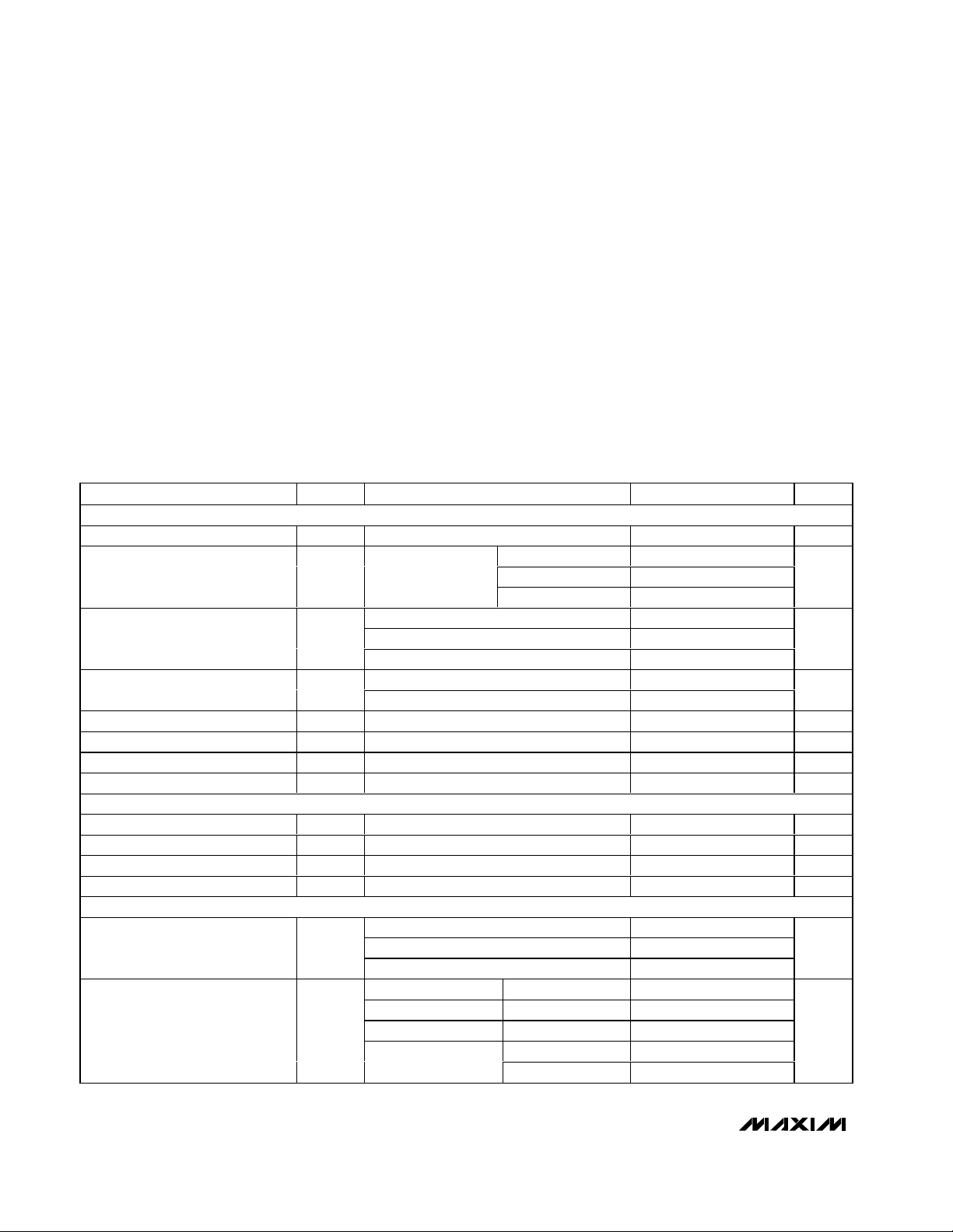
ELECTRICAL CHARACTERISTICS
(AVDD= DVDD= +5V ±5%, external reference = +4.096V, C
REF
= 10µF, C
REFADJ
= 0.1µF, V
REFADJ
= AVDD, TA= T
MIN
to T
MAX
,
unless otherwise noted. Typical values are at T
A
= +25°C.)
DC ACCURACY
Resolution RES 16 Bits
Integral Nonlinearity INL
Transition Noise
Offset Error -10 0 +10 mV
Gain Error 0 ±0.2 %FSR
Offset Drift 16 µV/°C
Gain Drift ±1 ppm/°C
AC ACCURACY (fIN = 1kHz, V
Signal-to-Noise Plus Distortion SINAD 86 90 dB
Signal-to-Noise Ratio SNR 87 91 dB
Total Harmonic Distortion THD -100 -92 dB
Spurious-Free Dynamic Range SFDR 92 103 dB
ANALOG INPUT
Input Range V
Input Resistance R
PARAMETER SYMBOL CONDITIONS MIN TYP MAX UNITS
= full range, 135ksps)
AIN
No missing codes
over temperature
MAX11_ _A -2 +2
MAX11_ _B -2 +2
MAX11_ _C -4 +4
RMS noise, external reference 0.6
Internal reference 0.75
MAX1179 -5 +5
MAX1187 0 +10
AIN
MAX1189 -10 +10
MAX1179/MAX1187 Normal operation 5.3 6.9 9.2
MAX1179 Shutdown mode 3
MAX1177 Shutdown mode 5.3
AIN
MAX1189
MAX11_ _A -1 +1
MAX11_ _B -1.0 +1.5Differential Nonlinearity DNL
MAX11_ _C -1 +2
Normal operation 7.8 10 13.0
Shutdown mode 6
LSB
LSB
LSB
V
kΩ
RMS
Page 3
MAX1179/MAX1187/MAX1189
16-Bit, 135ksps, Single-Supply ADCs with
Bipolar Analog Input Range
_______________________________________________________________________________________ 3
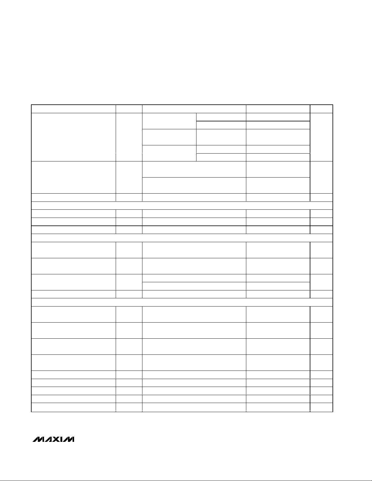
ELECTRICAL CHARACTERISTICS (continued)
(AVDD= DVDD= +5V ±5%, external reference = +4.096V, C
REF
= 10µF, C
REFADJ
= 0.1µF, V
REFADJ
= AVDD, TA= T
MIN
to T
MAX
,
unless otherwise noted. Typical values are at T
A
= +25°C.)
)
PARAMETER SYMBOL CONDITIONS MIN TYP MAX UNITS
MAX1179,
-5V ≤ V
AIN
Input Current I
AIN
MAX1187,
0 ≤ V
AIN
≤ +10V
MAX1189,
-10V ≤ V
AIN
MAX1179, V
Input Current Step at Power-Up I
PU
operating mode
MAX1189, V
operating mode
Input Capacitance C
IN
INTERNAL REFERENCE
REF Output Voltage V
REF
REF Output Tempco ±35 ppm/°C
REF Short-Circuit Current I
REF-(SC
EXTERNAL REFERENCE
REF and REFADJ Input Voltage
Range
REFADJ Buffer Disable Threshold
REF Input Current I
REFADJ Input Current I
REFADJ
Normal mode, f
REF
Shutdown mode (Note 1) ±0.1 ±10
REFADJ = AV
DIGITAL INPUTS/OUTPUTS
Output High Voltage V
Output Low Voltage V
Input High Voltage V
Input Low Voltage V
OH
OL
I
AV
I
AV
IH
IL
= 0.5mA, DVDD = +2.7V to +5.25V,
SOURCE
= +5.25V
DD
= 1.6mA, DVDD = +2.7V to +5.25V,
SINK
= +5.25V
DD
Input Leakage Current Digital input = DVDD or 0V -1 +1 µA
Input Hysteresis V
Input Capacitance C
Three-State Output Leakage I
Three-State Output Capacitance C
HYST
IN
OZ
OZ
Normal operation -1.8 +0.4
≤ +5V
Shutdown mode -1.8 +1.8
Normal/shutdown
mode
Normal operation -1.8 +1.2
≤ +10V
= +5V, shutdown mode to
AIN
= +10V, shutdown mode to
AIN
SAMPLE
DD
Shutdown mode -1.8 +1.8
= 135ksps 60 100
-0.1 +2.0
1 1.4
0.5 0.7
10 pF
4.056 4.096 4.136 V
±10 mA
3.8 4.2 V
AV
DD
0.4
-
AVDD -
0.1
16 µA
-
DV
DD
0.4
0.4 V
0.7 ×
DV
DD
0.3 ×
DV
DD
0.2 V
15 pF
±10 µA
15 pF
mA
mA
V
µA
V
V
V
Page 4
MAX1179/MAX1187/MAX1189
16-Bit, 135ksps, Single-Supply ADCs with
Bipolar Analog Input Range
4 _______________________________________________________________________________________
Note 1: Maximum specification is limited by automated test equipment.
Note 2: To ensure best performance, finish reading the data and wait t
BR
before starting a new acquisition.
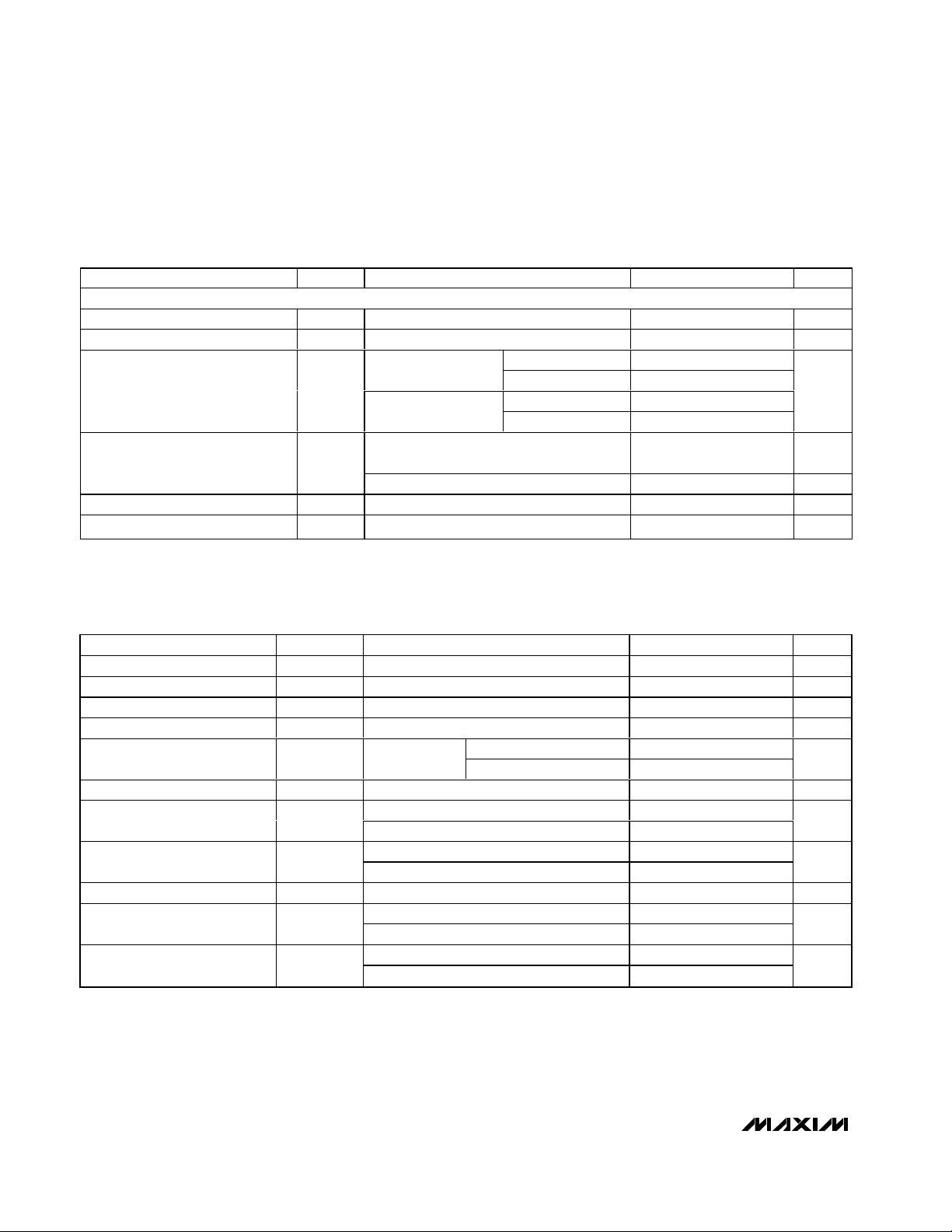
ELECTRICAL CHARACTERISTICS (continued)
(AVDD= DVDD= +5V ±5%, external reference = +4.096V, C
REF
= 10µF, C
REFADJ
= 0.1µF, V
REFADJ
= AVDD, TA= T
MIN
to T
MAX
,
unless otherwise noted. Typical values are at T
A
= +25°C.)
TIMING CHARACTERISTICS (Figures 1 and 2)
(AVDD= +5V ±5V, DVDD= +2.7V to AVDD, external reference = +4.096V, C
REF
= 10µF, C
REFADJ
= 0.1µF, V
REFADJ
= AVDD, C
LOAD
= 20pF, TA= T
MIN
to T
MAX
.)
DD
DD
AVDD
SHDN
DVDD
External reference,
135ksps
Internal reference,
135ksps
Shutdown mode, I
digital input = DV
Standby mode 3.7 mA
POWER SUPPLIES
Analog Supply Voltage AV
Digital Supply Voltage DV
Analog Supply Current I
Shutdown Supply Current I
Digital Supply Current I
Power-Supply Rejection AVDD = DVDD = +4.75V to +5.25V 3.5 LSB
PARAMETER SYMBOL CONDITIONS MIN TYP MAX UNITS
Maximum Sampling Rate f
Acquisition Time t
Conversion Time t
CS Pulse Width High t
CS Pulse Width Low t
R/C to CS Fall Setup Time t
R/C to CS Fall Hold Time t
CS to Output Data Valid t
EOC Fall to CS Fall t
CS Rise to EOC Rise t
Bus Relinquish Time t
PARAMETER SYMBOL CONDITIONS MIN TYP MAX UNITS
S AM P LE ( M A X )
ACQ
CONV
CSH
CSL
DS
DH
DO
DV
EOC
BR
(Note 2) 40 ns
(Note 2)
DVDD = +4.75V to +5.25V 40
DVDD = +2.7V to +5.25V 60
DVDD = +4.75V to +5.25V 40
DVDD = +2.7V to +5.25V 80
DVDD = +4.75V to +5.25V 40
DVDD = +2.7V to +5.25V 80
DVDD = +4.75V to +5.25V 40
DVDD = +2.7V to +5.25V 80
MAX1187 2.9
MAX1179/MAX1189 4.0 5.3
MAX1187 3.8
MAX1179/MAX1189 5.2 6.2
+ I
AVDD
DD
DVDD = +4.75V to +5.25V 40
DV
DVDD
or 0V
= +2.7V to +5.25V 60
DD
(Note 1),
4.75 5.25 V
2.70 5.25 V
0.5 5 µA
0.75 mA
2µs
0ns
0ns
135 ksps
4.7 µs
mA
ns
ns
ns
ns
ns
Page 5
MAX1179/MAX1187/MAX1189
16-Bit, 135ksps, Single-Supply ADCs with
Bipolar Analog Input Range
_______________________________________________________________________________________ 5
Typical Operating Characteristics
(AVDD= DVDD= +5V, external reference = +4.096V, C
REF
= 10µF, C
REFADJ
= 0.1µF, V
REFADJ
= AVDD, C
LOAD
= 20pF, TA= T
MIN
to
T
MAX
, unless otherwise noted. Typical values are at TA= +25°C.) (Typical Application Circuit)
INL vs. CODE
2.5
2.0
1.5
1.0
0.5
0
INL (LSB)
-0.5
-1.0
-1.5
-2.0
-2.5
0
CODE
600002000010000 30000 5000040000
MAX1179/87/89 toc01
DNL (LSB)
2.5
2.0
1.5
1.0
0.5
0
-0.5
-1.0
-1.5
-2.0
-2.5
DNL vs. CODE
CODE
600002000010000 30000 50000400000
4.80
4.75
4.70
MAX1179/87/89 toc02
4.65
4.60
4.55
SUPPLY CURRENT (mA)
4.50
4.45
4.40
SUPPLY CURRENT (AVDD + DVDD)
vs. TEMPERATURE
5.25V
5.0V
4.75V
f
= 135ksps
SAMPLE
SHUTDOWN MODE BETWEEN
-40 80
TEMPERATURE (°C)
CONVERSIONS
6040-20 0 20
MAX1179/87/89 toc03
SUPPLY CURRENT (AVDD + DVDD)
vs. SAMPLE RATE
10
STANDBY MODE
1
0.1
0.01
SUPPLY CURRENT (mA)
0.001
0.0001
0.01 1000
SHUTDOWN MODE
SAMPLE RATE (ksps)
GAIN ERROR
vs. TEMPERATURE
0.20
0.15
0.10
0.05
0
-0.05
GAIN ERROR (%FSR)
-0.10
-0.15
-0.20
-40 0-20 20 40 60 80
TEMPERATURE (°C)
SHUTDOWN CURRENT (AVDD + DVDD)
5.0
vs. TEMPERATURE
NO CONVERSIONS
4.5
4.0
MAX1179/87/89 toc04
3.5
3.0
2.5
2.0
1.5
1.0
SHUTDOWN SUPPLY CURRENT (µA)
0.5
0
1001010.1
-40 80
TEMPERATURE (°C)
6040-20 0 20
MAX1179/87/89 toc05
OFFSET ERROR vs. TEMPERATURE
10
MAX1189
8
6
4
2
0
-2
OFFSET ERROR (mV)
-4
-6
-8
-10
-40 80
TEMPERATURE (°C)
MAX1179/87/89 toc06
6040-20 0 20
INTERNAL REFERENCE
4.136
4.126
4.116
MAX1179/87/89 toc07
4.106
4.096
4.086
INTERNAL REFERENCE (V)
4.076
4.066
4.056
-40 0-20 20 40 60 80
vs. TEMPERATURE
TEMPERATURE (°C)
MAX1179/87/89 toc08
-100
MAGNITUDE (dB)
-120
-140
-160
-180
0
f
SAMPLE
-20
-40
-60
-80
060
FFT AT 1kHz
= 135ksps
MAX 1179/87/89 toc09
4020
FREQUENCY (kHz)
Page 6

MAX1179/MAX1187/MAX1189
16-Bit, 135ksps, Single-Supply ADCs with
Bipolar Analog Input Range
6 _______________________________________________________________________________________
Pin Description
Typical Operating Characteristics (continued)
(AVDD= DVDD= +5V, external reference = +4.096V, C
REF
= 10µF, C
REFADJ
= 0.1µF, V
REFADJ
= AVDD, C
LOAD
= 20pF, TA= T
MIN
to
T
MAX
, unless otherwise noted. Typical values are at TA= +25°C.) (Typical Application Circuit)
SINAD vs. FREQUENCY
100
90
80
70
60
50
SINAD (dB)
40
30
20
10
f
= 131ksps
SAMPLE
0
1 100
10
FREQUENCY (kHz)
120
100
MAX1179/87/89 toc10
80
60
SFDR (dB)
40
20
0
SPURIOUS-FREE DYNAMIC RANGE
vs. FREQUENCY
1 100
10
FREQUENCY (kHz)
MAX1179/87/89 toc11
THD (dB)
TOTAL HARMONIC DISTORTION
vs. FREQUENCY
0
-10
-20
-30
-40
-50
-60
-70
-80
-90
-100
-110
1 100
FREQUENCY (kHz)
MAX1179/87/89 toc12
10
PIN NAME FUNCTION
1 D8 Three-State Digital Data Output
2 D9 Three-State Digital Data Output
3 D10 Three-State Digital Data Output
4 D11 Three-State Digital Data Output
5 D12 Three-State Digital Data Output
6 D13 Three-State Digital Data Output
7 D14 Three-State Digital Data Output
8 D15 Three-State Digital Data Output (MSB)
Read/Convert Input. Power up and place the MAX1179/MAX1187/MAX1189 in acquisition mode by
holding R/C low during the first falling edge of CS. During the second falling edge of CS, the level
9R/C
on R/C determines whether the reference and reference buffer power down or remain on after
conversion. Set R/C high during the second falling edge of CS to power down the reference and
buffer, or set R/C low to leave the reference and buffer powered up. Set R/C high during the third
falling edge of CS to put valid data on the bus.
10 EOC End of Conversion. EOC drives low when conversion is complete.
11 AV
DD
Analog Supply Input. Bypass with a 0.1µF capacitor to AGND.
12 AGND Analog Ground. Primary analog ground (star ground).
13 AIN Analog Input
14 AGND Analog Ground. Connect pin 14 to pin 12.
Page 7

Detailed Description
Converter Operation
The MAX1179/MAX1187/MAX1189 use a successiveapproximation (SAR) conversion technique with an
inherent track-and-hold (T/H) stage to convert an analog input into a 16-bit digital output. Parallel outputs
provide a high-speed interface to microprocessors
(µPs). The Functional Diagram at the end of the data
sheet shows a simplified internal architecture of the
MAX1179/MAX1187/MAX1189. Figure 3 shows a typical
application circuit for the MAX1179/MAX1187/MAX1189.
Analog Input
Input Scaler
The MAX1179/MAX1187/MAX1189 have an input scaler
which allows conversion of true bipolar input voltages
and input voltages greater than the power supply, while
operating from a single +5V analog supply. The input
scaler attenuates and shifts the analog input to match
the input range of the internal DAC. The MAX1179 input
voltage range is ±5V, while the MAX1189 input voltage
range is ±10V. The MAX1187 has a unipolar input voltage range of 0 to +10V. Figure 4 shows the equivalent
input circuit of the MAX1179/MAX1187/MAX1189. This
circuit limits the current going into or out of AIN to less
than 1.8mA.
MAX1179/MAX1187/MAX1189
16-Bit, 135ksps, Single-Supply ADCs with
Bipolar Analog Input Range
_______________________________________________________________________________________ 7
Pin Description (continued)
Figure 1. Load Circuits
PIN NAME FUNCTION
15 REFADJ
16 REF
Reference Buffer Output. Bypass REFADJ with a 0.1µF capacitor to AGND for internal reference
mode. Connect REFADJ to AV
to select external reference mode.
DD
Reference Input/Output. Bypass REF with a 10µF capacitor to AGND. REF is the external reference
input when in external reference mode.
17 RESET Reset Input. Logic high resets the device.
Convert Start. The first falling edge of CS powers up the device and enables acquisition when R/C
18 CS
is low. The second falling edge of CS starts conversion. The third falling edge of CS loads the result
onto the bus when R/C is high.
19 DGND Digital Ground
20 DV
DD
Digital Supply Voltage. Bypass with a 0.1µF capacitor to DGND.
21 D0 Three-State Digital Data Output (LSB)
22 D1 Three-State Digital Data Output
23 D2 Three-State Digital Data Output
24 D3 Three-State Digital Data Output
25 D4 Three-State Digital Data Output
26 D5 Three-State Digital Data Output
27 D6 Three-State Digital Data Output
28 D7 Three-State Digital Data Output
DV
DD
1mA
D0–D15
1mA
A)
HIGH-Z TO V
V
OL
V
OH
DGND
OH
TO VOH, AND
TO HIGH-Z
= 20pF
C
LOAD
,
D0–D15
B)
HIGH-Z TO V
TO VOL, AND
V
OH
TO HIGH-Z
V
OL
= 20pF
C
LOAD
DGND
,
OL
Page 8

MAX1179/MAX1187/MAX1189
Track and Hold (T/H)
In track mode, the internal hold capacitor acquires the
analog signal (see Figure 4). In hold mode, the T/H
switches open and the capacitive DAC samples the
analog input. During the acquisition, the analog input
(AIN) charges capacitor C
HOLD
. The acquisition ends
on the second falling edge of CS. At this instant, the
T/H switches open. The retained charge on C
HOLD
represents a sample of the input. In hold mode, the capacitive DAC adjusts during the remainder of the
conversion time to restore node T/H OUT to zero within
the limits of a 16-bit resolution. Force CS low to put
valid data on the bus after conversion is complete.
Power-Down Modes
Select standby mode or shutdown mode with R/C during
the second falling edge of CS (see Selecting Standby or
Shutdown Mode section). The MAX1179/MAX1187/
MAX1189 automatically enter either standby mode (reference and buffer on) or shutdown (reference and buffer
off) after each conversion depending on the status of
R/C during the second falling edge of CS.
Internal Clock
The MAX1179/MAX1187/MAX1189 generate an internal
conversion clock to free the microprocessor from the burden of running the SAR conversion clock. Total conversion time after entering hold mode (second falling edge of
CS) to end-of-conversion (EOC) falling is 4.7µs (max).
Applications Information
Starting a Conversion
CS and R/C control acquisition and conversion in the
MAX1179/MAX1187/MAX1189 (see Figure 2). The first
falling edge of CS powers up the device and puts it in
acquire mode if R/C is low. The convert start (CS) is
ignored if R/C is high. The MAX1179/MAX1187/
MAX1189 need at least 12ms (C
REFADJ
= 0.1µF, C
REF
= 10µF) for the internal reference to wake up and settle
before starting the conversion, if powering up from
shutdown. Reset the MAX1179/MAX1187/ MAX1189 by
toggling RESET with CS high. The next falling edge of
CS begins acquisition.
Selecting Standby or Shutdown Mode
The MAX1179/MAX1187/MAX1189 have a selectable
standby or low-power shutdown mode. In standby
mode, the ADC’s internal reference and reference
buffer do not power down between conversions, eliminating the need to wait for the reference to power up
before performing the next conversion. Shutdown mode
powers down the reference and reference buffer after
16-Bit, 135ksps, Single-Supply ADCs with
Bipolar Analog Input Range
8 _______________________________________________________________________________________
Figure 2. MAX1179/MAX1187/MAX1189 Timing Diagram
Figure 3. Typical Application Circuit for the MAX1179/MAX1187/
MAX1189
t
CSLtCSH
CS
t
ACQ
R/C
t
DH
EOC
HIGH-Z
D0–D15
REF POWER-
DOWN CONTROL
t
DS
t
CONV
t
t
DV
t
DO
DATA VALID
EOC
t
BR
HIGH-Z
+5V ANALOG +5V DIGITAL
ANALOG
INPUT
AIN
0.1µF0.1µF
µP DATA
AV
DD
DV
DD
D0–D15
BUS
16-BIT
WIDE
MAX1179
MAX1187
R/C
MAX1189
CS
RESET
EOC
REF
REFADJ
AGND DGND
0.1µF
10µF
Page 9

completing a conversion. The reference and reference
buffer require a minimum of 12ms (C
REFADJ
= 0.1µF,
C
REF
= 10µF) to power up and settle from shutdown.
The state of R/C during the second falling edge of CS
selects which power-down mode the MAX1179/
MAX1187/MAX1189 enters upon conversion completion. Holding R/C low causes the MAX1179/MAX1187/
MAX1189 to enter standby mode. The reference and
buffer are left on after the conversion completes. R/C
high causes the MAX1179/MAX1187/MAX1189 to enter
shutdown mode and power down the reference and
buffer after conversion (see Figures 5 and 6). Set the
voltage at REF high during the second falling edge of
CS to realize the lowest current operation.
Standby Mode
While in standby mode, the supply current is less than
3.7mA (typ). The next falling edge of CS with R/C low
causes the MAX1179/MAX1187/MAX1189 to exit standby mode and begin acquisition. The reference and reference buffer remain active to allow quick turn-on time.
MAX1179/MAX1187/MAX1189
16-Bit, 135ksps, Single-Supply ADCs with
Bipolar Analog Input Range
_______________________________________________________________________________________ 9
Figure 4. Equivalent Input Circuit
AIN
Figure 5. Selecting Standby Mode
REF
R2
MAX1187
161Ω
R3
3.4kΩ
TRACK
S1
HOLD
C
HOLD
30pF
TRACK
T/H OUT
HOLD
S2
AIN
MAX1179/MAX1189
R2
161Ω
R3
POWER-
DOWN
S3
3.4kΩ
TRACK
S1
HOLD
C
HOLD
30pF
TRACK
T/H OUT
HOLD
S2
S1, S2 = T/H SWITCH
S3 = POWER-DOWN
(MAX1179/MAX1189
ONLY)
ACQUISITION CONVERSION
CS
R/C
EOC
REF AND
BUFFER
POWER
R2 = 7.85kΩ (MAX1189)
OR 3.92kΩ (MAX1179/MAX1187)
R3 = 5.45kΩ (MAX1189)
OR 17.79kΩ (MAX1179/MAX1187)
DATA
OUT
Page 10

MAX1179/MAX1187/MAX1189
Shutdown Mode
In shutdown mode, the reference and reference buffer
shut down between conversions. Shutdown mode
reduces supply current to 0.5µA (typ) immediately after
the conversion. The next falling edge of CS with R/C
low causes the reference and buffer to wake up and
enter acquisition mode. To achieve 16-bit accuracy,
allow 12ms (C
REFADJ
= 0.1µF, C
REF
= 10µF) for the
internal reference to wake up.
Internal and External Reference
Internal Reference
The internal reference of the MAX1179/MAX1187/
MAX1189 is internally buffered to provide +4.096V output at REF. Bypass REF to AGND and REFADJ to
AGND with 10µF and 0.1µF, respectively.
Sink or source current at REFADJ to make fine adjustments to the internal reference. The input impedance of
REFADJ is nominally 5kΩ. Use the circuit of Figure 7 to
adjust the internal reference to ±1.5%.
External Reference
An external reference can be placed at either the input
(REFADJ) or the output (REF) of the MAX1179/
MAX1187/MAX1189’s internal buffer amplifier. Using
the buffered REFADJ input makes buffering the external
reference unnecessary. The input impedance of
REFADJ is typically 5kΩ. The internal buffer output
must be bypassed at REF with a 10µF capacitor.
Connect REFADJ to AVDDto disable the internal buffer.
Directly drive REF using an external 3.8V to 4.2V reference. During conversion, the external reference must
be able to drive 100µA of DC load current and have an
output impedance of 10Ω or less.
For optimal performance, buffer the reference through
an op amp and bypass REF with a 10µF capacitor.
Consider the MAX1179/MAX1187/MAX1189’s equivalent
input noise (0.6LSB) when choosing a reference.
Reading the Conversion Result
EOC flags the microprocessor when a conversion is
complete. The falling edge of EOC signals that the data
is valid and ready to be output to the bus. D0–D15 are
the parallel outputs of the MAX1179/MAX1187/
MAX1189. These three-state outputs allow for direct
connection to a microcontroller I/O bus. The outputs
remain high-impedance during acquisition and conversion. Data is loaded onto the bus with the third falling
edge of CS with R/C high (after tDO). Bringing CS high
forces the output bus back to high impedance. The
MAX1179/MAX1187/MAX1189 then wait for the next
falling edge of CS to start the next conversion cycle
(see Figure 2).
16-Bit, 135ksps, Single-Supply ADCs with
Bipolar Analog Input Range
10 ______________________________________________________________________________________
Figure 6. Selecting Shutdown Mode
Figure 7. MAX1179/MAX1187/MAX1189 Reference Adjust
Circuit
ACQUISITION CONVERSION
CS
R/C
EOC
REF &
BUFFER
POWER
MAX1179
MAX1187
MAX1189
REFADJ
100kΩ
150kΩ
+5V
68kΩ
0.1µF
DATA
OUT
Page 11

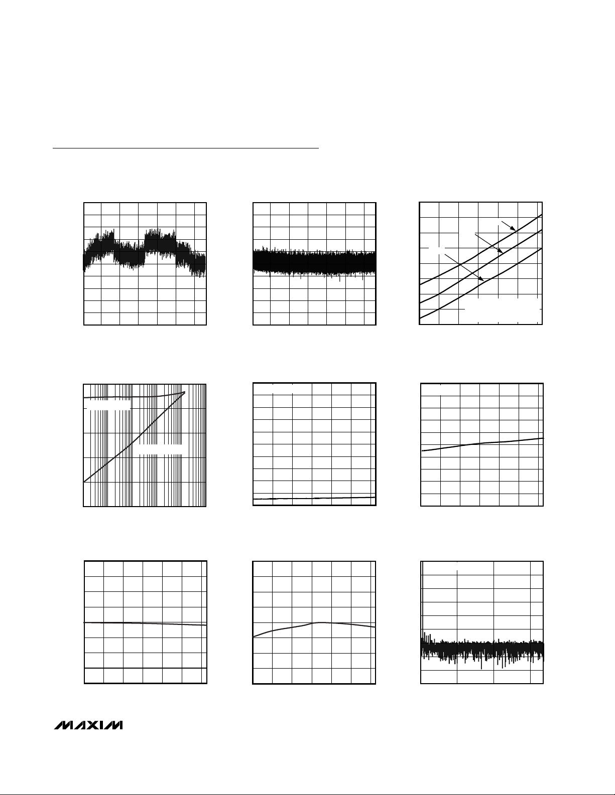
Transfer Function
Figures 8, 9, and 10 show the MAX1179/MAX1187/
MAX1189’s output transfer functions. The MAX1179
and MAX1189 outputs are coded in offset binary, while
the MAX1187 is coded in standard binary.
Input Buffer
Most applications require an input buffer amplifier to
achieve 16-bit accuracy and prevent loading the
source. Switch the channels immediately after acquisition, rather than near the end of or after a conversion
when the input signal is multiplexed. This allows more
time for the input buffer amplifier to respond to a large
step-change in input signal. The input amplifier must
have a high enough slew rate to complete the required
output voltage change before the beginning of the
acquisition time. Figure 11 shows an example of this
circuit using the MAX427.
Figures 12a and 12b show how the MAX1179 and
MAX1189 analog input current varies depending on
whether the chip is operating or powered down. The
part is fully powered down between conversions if the
voltage at R/C is set high during the second falling
edge of CS. The input current abruptly steps to the
powered up value at the start of acquisition. This step
in the input current can disrupt the ADC input, depending on the driving circuit’s output impedance at high
frequencies. If the driving circuit cannot fully settle by
the end of acquisition time, the accuracy of the system
can be compromised. To avoid this situation, increase
the acquisition time, use a driving circuit that can settle
within t
ACQ
, or leave the MAX1179/MAX1189 powered
up by setting the voltage at R/C low during the second
falling edge of CS.
Layout, Grounding, and Bypassing
For best performance, use printed circuit (PC) boards.
Do not run analog and digital lines parallel to each
other, and do not lay out digital signal paths underneath the ADC package. Use separate analog and digital ground planes with only one point connecting the
two ground systems (analog and digital) as close to the
device as possible.
Route digital signals far away from sensitive analog and
reference inputs. If digital lines must cross analog lines,
do so at right angles to minimize coupling digital noise
MAX1179/MAX1187/MAX1189
16-Bit, 135ksps, Single-Supply ADCs with
Bipolar Analog Input Range
______________________________________________________________________________________ 11
Figure 9. MAX1187 Transfer Function
Figure 10. MAX1189 Transfer Function
Figure 8. MAX1179 Transfer Function
OUTPUT CODE
11 . . . 1111
11 . . . 1110
11 . . . 1101
10 . . . 0001
10 . . . 0000
01 . . . 1111
00 . . . 0011
00 . . . 0010
00 . . . 0001
00 . . . 0000
-32768 +32768
-32767 -32765 +32767
INPUT RANGE = -5V TO +5V
FULL-SCALE
TRANSITION
FULL-SCALE RANGE
(FSR) = +10V
1LSB =
0-32766
-1 +1
INPUT VOLTAGE (LSB)
+32766
FSR x V
REF
65536 x 4.096
OUTPUT CODE
11 . . . 1111
11 . . . 1110
11 . . . 1101
10 . . . 0001
10 . . . 0000
01 . . . 1111
00 . . . 0011
00 . . . 0010
00 . . . 0001
00 . . . 0000
-32768 +32768
-32767 -32765 +32767
INPUT RANGE = -10V TO +10V
FULL-SCALE
TRANSITION
FULL-SCALE RANGE
(FSR) = +20V
1LSB =
0-32766
-1 +1
INPUT VOLTAGE (LSB)
+32766
FSR x V
REF
65536 x 4.096
OUTPUT CODE
11 . . . 111
11 . . . 110
11 . . . 101
00 . . . 011
00 . . . 010
00 . . . 001
00 . . . 000
2103
INPUT RANGE = 0 TO +10V
FULL-SCALE
TRANSITION
INPUT VOLTAGE (LSB)
FULL-SCALE RANGE
(FSR) = +10V
FSR x V
1LSB =
65536 x 4.096
65534
65536
65535
REF
Page 12

MAX1179/MAX1187/MAX1189
onto the analog lines. If the analog and digital sections
share the same supply, isolate the digital and analog
supply by connecting them with a low value (10Ω)
resistor or ferrite bead.
The ADC is sensitive to high-frequency noise on the
AVDDsupply. Bypass AVDDto AGND with a 0.1µF
capacitor in parallel with a 1µF to 10µF low-ESR capacitor with the smallest capacitor closest to the device.
Keep capacitor leads short to minimize stray inductance.
Definitions
Integral Nonlinearity
Integral nonlinearity (INL) is the deviation of the values
on an actual transfer function from a straight line. This
straight line can be either a best-straight-line fit or a line
drawn between the end points of the transfer function,
once offset and gain errors have been nullified. The
static linearity parameters for the MAX1179/MAX1187/
MAX1189 are measured using the endpoint method.
Differential Nonlinearity
Differential nonlinearity (DNL) is the difference between
an actual step-width and the ideal value of 1LSB. A
DNL error specification of 1LSB guarantees no missing
codes and a monotonic transfer function.
Signal-to-Noise Ratio
For a waveform perfectly reconstructed from digital
samples, signal-to-noise ratio (SNR) is the ratio of the
full-scale analog input (RMS value) to the RMS quantization error (residual error). The ideal, theoretical minimum analog-to-digital noise is caused by quantization
noise error only and results directly from the ADC’s resolution (N bits):
SNR = ((6.02 ✕N) + 1.76)dB
where N = 16 bits.
In reality, there are other noise sources besides quantization noise: thermal noise, reference noise, clock jitter,
16-Bit, 135ksps, Single-Supply ADCs with
Bipolar Analog Input Range
12 ______________________________________________________________________________________
Figure 12a. MAX1179 Analog Input Current
Figure 12b. MAX1189 Analog Input Current
Figure 11. MAX1179/MAX1187/MAX1189 Fast-Settling Input
Buffer
REF
MAX1179
MAX1187
MAX1189
**
ANALOG
INPUT
MAX427
AIN
*
*MAX1187 ONLY.
**MAX1179/MAX1189 ONLY.
MAX1179
ANALOG INPUT CURRENT
vs. ANALOG INPUT VOLTAGE
2.0
1.5
1.0
0.5
SHUTDOWN MODE
0
-0.5
-1.0
ANALOG INPUT CURRENT (mA)
-1.5
-2.0
-5.0 5.0
ANALOG INPUT VOLTAGE (V)
STANDBY MODE
2.50-2.5
1.5
1.0
0.5
SHUTDOWN MODE
0
-0.5
ANALOG INPUT CURRENT (mA)
-1.0
-1.5
-10 10
MAX1189
ANALOG INPUT CURRENT
vs. ANALOG INPUT VOLTAGE
STANDBY MODE
ANALOG INPUT VOLTAGE (V)
50-5
Page 13

etc. SNR is computed by taking the ratio of the RMS
signal to the RMS noise, which includes all spectral
components minus the fundamental, the first five harmonics, and the DC offset.
Signal-to-Noise Plus Distortion
Signal-to-noise plus distortion (SINAD) is the ratio of the
fundamental input frequency’s RMS amplitude to the
RMS equivalent of all the other ADC output signals.
Effective Number of Bits
Effective number of bits (ENOB) indicates the global
accuracy of an ADC at a specific input frequency and
sampling rate. An ideal ADC’s error consists of quantization noise only. With an input range equal to the fullscale range of the ADC, calculate the effective number
of bits as follows:
Total Harmonic Distortion
Total harmonic distortion (THD) is the ratio of the RMS
sum of the first five harmonics of the input signal to the
fundamental itself. This is expressed as:
where V1is the fundamental amplitude and V2through
V5are the 2nd- through 5th-order harmonics.
Spurious-Free Dynamic Range
Spurious-free dynamic range (SFDR) is the ratio of the
RMS amplitude of the fundamental (maximum signal
component) to the RMS value of the next largest frequency component.
Chip Information
TRANSISTOR COUNT: 15,383
PROCESS: BiCMOS
MAX1179/MAX1187/MAX1189
16-Bit, 135ksps, Single-Supply ADCs with
Bipolar Analog Input Range
______________________________________________________________________________________ 13
Ordering Information (continued)
*Future product—contact factory for availability.
()
=×
20 log
SINAD db
Signal
RMS
()
+
Noise Distortion
RMS
THD
=
20 log
×
SINAD - 1.76
E
NOB
=
602.
PART TEMP RANGE PIN-PACKAGE
MAX1179CCUI 0°C to +70°C 28 TSSOP ±5V ±4
MAX1179AEUI -40°C to +85°C 28 TSSOP ±5V ±2
MAX1179BEUI -40°C to +85°C 28 TSSOP ±5V ±2
MAX1179CEUI -40°C to +85°C 28 TSSOP ±5V ±4
MAX1187ACUI 0°C to +70°C 28 TSSOP 0 to +10V ±2
MAX1187BCUI 0°C to +70°C 28 TSSOP 0 to +10V ±2
MAX1187CCUI 0°C to +70°C 28 TSSOP 0 to +10V ±4
MAX1187AEUI -40°C to +85°C 28 TSSOP 0 to +10V ±2
MAX1187BEUI -40°C to +85°C 28 TSSOP 0 to +10V ±2
MAX1187CEUI -40°C to +85°C 28 TSSOP 0 to +10V ±4
MAX1189ACUI 0°C to +70°C 28 TSSOP ±10V ±2
MAX1189BCUI 0°C to +70°C 28 TSSOP ±10V ±2
MAX1189CCUI 0°C to +70°C 28 TSSOP ±10V ±4
MAX1189AEUI* -40°C to +85°C 28 TSSOP ±10V ±2
MAX1189BEUI* -40°C to +85°C 28 TSSOP ±10V ±2
MAX1189CEUI* -40°C to +85°C 28 TSSOP ±10V ±4
INPUT VOLTAGE
V+V+V+V
223
242
V
1
RANGE
INL (LSB)
2
5
Page 14

MAX1179/MAX1187/MAX1189
16-Bit, 135ksps, Single-Supply ADCs with
Bipolar Analog Input Range
14 ______________________________________________________________________________________
Functional Diagram
REFADJ AV
5kΩ
REFERENCE
OUTPUT
REGISTERS
REF
CLOCK
CAPACITIVE
DAC
SUCCESSIVE-
APPROXIMATION
REGISTER AND
CONTROL LOGIC
AIN
AGND
RESET
CS
R/C
INPUT
SCALER
DV
AGND DGND
DD
16 BITS
MAX1179
MAX1187
MAX1189
DD
16 BITS
D0–D15
EOC
Page 15

MAX1179/MAX1187/MAX1189
16-Bit, 135ksps, Single-Supply ADCs with
Bipolar Analog Input Range
Maxim cannot assume responsibility for use of any circuitry other than circuitry entirely embodied in a Maxim product. No circuit patent licenses are
implied. Maxim reserves the right to change the circuitry and specifications without notice at any time.
Maxim Integrated Products, 120 San Gabriel Drive, Sunnyvale, CA 94086 408-737-7600 ____________________ 15
© 2003 Maxim Integrated Products Printed USA is a registered trademark of Maxim Integrated Products.
Package Information
(The package drawing(s) in this data sheet may not reflect the most current specifications. For the latest package outline information,
go to www.maxim-ic.com/packages.)
TSSOP4.40mm.EPS
 Loading...