

Page 1
19-1081; Rev 1; 8/96
+3V, 400ksps, 4/8-Channel,
8-Bit ADCs with 1µA Power-Down
_______________General Description
The MAX113/MAX117 are microprocessor-compatible,
8-bit, 4-channel and 8-channel analog-to-digital converters (ADCs). They operate from a single +3V supply
and use a half-flash technique to achieve a 1.8µs conversion time (400ksps). A power-down pin (PWRDN)
reduces current consumption to 1µA typical. The
devices return from power-down mode to normal operating mode in less than 900ns, allowing large supplycurrent reductions in burst-mode applications. (In burst
mode, the ADC wakes up from a low-power state at
specified intervals to sample the analog input signals.)
Both converters include a track/hold, enabling the ADC
to digitize fast analog signals.
____________________________Features
♦ +3.0V to +3.6V Single-Supply Operation
♦ 4 (MAX113) or 8 (MAX117) Analog Input Channels
♦ Low Power: 1.5mA (operating mode)
1µA (power-down mode)
♦ Total Unadjusted Error ≤ 1LSB
♦ Fast Conversion Time: 1.8µs per Channel
♦ No External Clock Required
♦ Internal Track/Hold
♦ Ratiometric Reference Inputs
♦ Internally Connected 8th Channel Monitors
Reference Voltage (MAX117)
Microprocessor (µP) interfaces are simplified because
the ADC can appear as a memory location or I/O port
without external interface logic. The data outputs use
latched, three-state buffer circuitry for direct connection
to an 8-bit parallel µP data bus or system input port.
The MAX113/MAX117 input/reference configuration
enables ratiometric operation.
The 4-channel MAX113 is available in a 24-pin DIP or
SSOP. The 8-channel MAX117 is available in a 28-pin
DIP or SSOP. For +5V applications, refer to the
MAX114/MAX118 data sheet.
________________________Applications
Battery-Powered Systems Portable Equipment
System-Health Monitoring Remote Data Acquisition
Communications Systems
______________Ordering Information
PART
MAX113CNG
MAX113CAG
MAX113C/D 0°C to +70°C
MAX113ENG
MAX113EAG
MAX113MRG -55°C to +125°C
Ordering Information continued at end of data sheet.
*Dice are specified at T
**Contact factory for availability.
Pin Configuration appears at end of data sheet.
TEMP. RANGE
0°C to +70°C
0°C to +70°C
-40°C to +85°C 24 Narrow Plastic DIP
-40°C to +85°C
= +25°C, DC parameters only.
A
PIN-PACKAGE
24 Narrow Plastic DIP
24 SSOP
Dice*
24 SSOP
24 Narrow CERDIP**
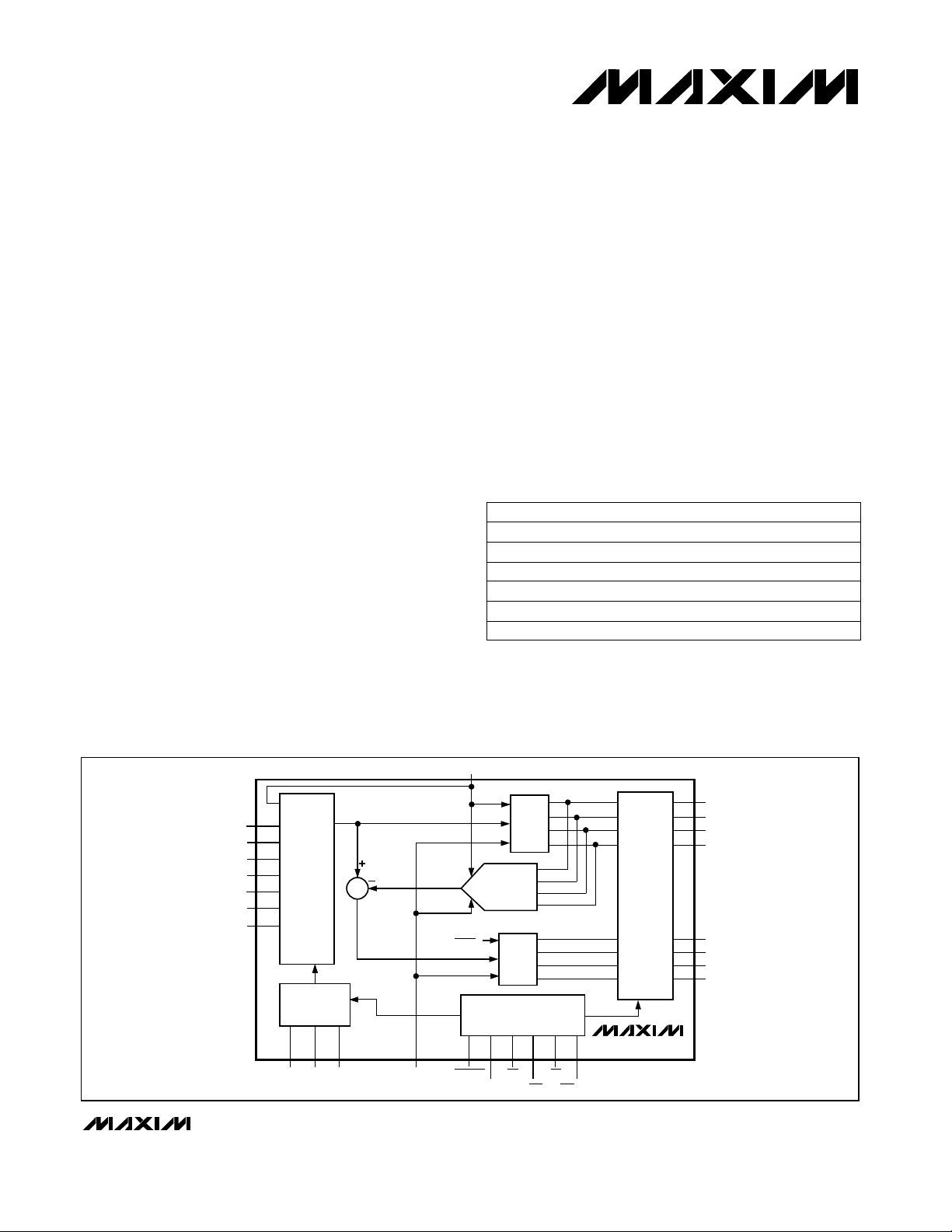
_________________________________________________________Functional Diagram
MAX113/MAX117
REF+
D7
D6
D5
D4
D3
D2
D1
D0
Maxim Integrated Products
1
MODE
4-BIT
FLASH
ADC
(4MSBs)
4-BIT
DAC
4-BIT
FLASH
ADC
(4LSBs)
TIMING AND
CONTROL
RD
INT
CS
WR/RDY
*IN8
*IN7
*IN6
*IN5
IN4
IN3
IN2
IN1
*MAX117 ONLY
________________________________________________________________
MUX
ADDRESS
LATCH
DECODE
A0
Σ
A1 A2 REF-
REF+
16
PWRDN
THREE-
STATE
OUTPUT
DRIVERS
MAX113/MAX117
For free samples & the latest literature: http://www.maxim-ic.com, or phone 1-800-998-8800
Page 2
+3V, 400ksps, 4/8-Channel,
8-Bit ADCs with 1µA Power-Down
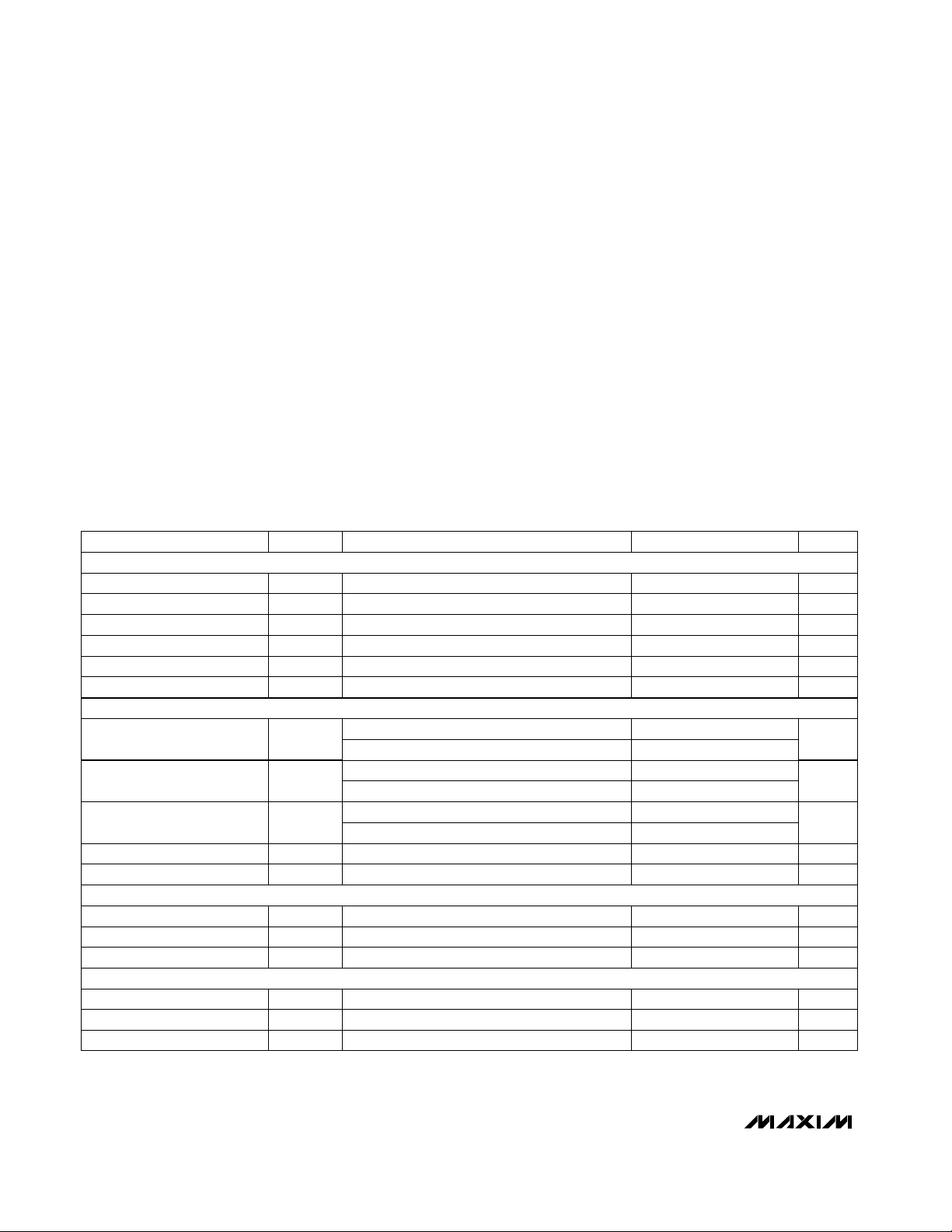
ABSOLUTE MAXIMUM RATINGS
VDDto GND..............................................................-0.3V to +7V
Digital Input Voltage to GND......................-0.3V to (V
Digital Output Voltage to GND...................-0.3V to (V
REF+ to GND..............................................-0.3V to (V
REF- to GND...............................................-0.3V to (V
IN_ to GND.................................................-0.3V to (V
Continuous Power Dissipation (T
24 Narrow Plastic DIP
(derate 13.33mW/°C above +70°C)................................1.08W
24 SSOP (derate 8.00mW/°C above +70°C).................640mW
24 Narrow CERDIP (derate 12.50mW/°C above +70°C) .....1W
Stresses beyond those listed under “Absolute Maximum Ratings” may cause permanent damage to the device. These are stress ratings only, and functional
operation of the device at these or any other conditions beyond those indicated in the operational sections of the specifications is not implied. Exposure to
absolute maximum rating conditions for extended periods may affect device reliability.
= +70°C)
A
DD
DD
DD
DD
DD
+ 0.3V)
+ 0.3V)
+ 0.3V)
+ 0.3V)
+ 0.3V)
28 Wide Plastic DIP
(derate 14.29mW/°C above +70°C)................................1.14W
28 SSOP (derate 9.52mW/°C above +70°C).................762mW
28 Wide CERDIP (derate 16.67mW/°C above +70°C)....1.33W
Operating Temperature Ranges
MAX113C_G/MAX117C_I ....................................0°C to +70°C
MAX113E_G/MAX117E_I..................................-40°C to +85°C
MAX113MRG/MAX117MJI..............................-55°C to +125°C
Storage Temperature Range.............................-65°C to +150°C
Lead Temperature (soldering, 10sec).............................+300°C
MAX113/MAX117
ELECTRICAL CHARACTERISTICS
(VDD= +3V to +3.6V, REF+ = 3V, REF- = GND, Read Mode (MODE = GND), TA= T
CONDITIONS
ACCURACY (Note 1)
No-missing-codes guaranteed
DYNAMIC PERFORMANCE
Signal-to-Noise Plus
Distortion Ratio
Spurious-Free Dynamic
Range
ANALOG INPUT
REFERENCE INPUT
Reference Resistance
REF+ Input Voltage Range
REF- Input Voltage Range
SINAD
THDTotal Harmonic Distortion
SFDR
VIN_Input Voltage Range
REF
MAX11_C/E, f
MAX11_M, f
MAX11_C/E, f
MAX11_M, f
MAX11_C/E, f
MAX11_M, f
V
= 3Vp-p
IN_
GND < V
IN_
SAMPLE
SAMPLE
SAMPLE
< V
= 400kHz, fIN= 30.273kHz
SAMPLE
= 340kHz, fIN= 30.725kHz
= 400kHz, fIN= 30.273kHz
SAMPLE
= 340kHz, fIN= 30.725kHz
= 400kHz, fIN= 30.273kHz
SAMPLE
= 340kHz, fIN= 30.725kHz
DD
MIN
to T
, unless otherwise noted.)
MAX
45
45
50
50
REF-
REF-
V
V
UNITSMIN TYP MAXSYMBOLPARAMETER
LSB±1TUETotal Unadjusted Error
LSB±1DNLDifferential Nonlinearity
LSB±1Zero-Code Error
LSB±1Full-Scale Error
LSB±1/4Channel-to-Channel Mismatch
-50
-50
MHz0.3Input Full-Power Bandwidth
V/µs0.28 0.5Input Slew Rate, Tracking
REF+
DD
REF+
Bits8NResolution
dB
dB
dB
VV
µA±3IIN_Input Leakage Current
pF32CIN_Input Capacitance
kΩ124R
VV
VGND V
2 _______________________________________________________________________________________
Page 3
+3V, 400ksps, 4/8-Channel,
8-Bit ADCs with 1µA Power-Down
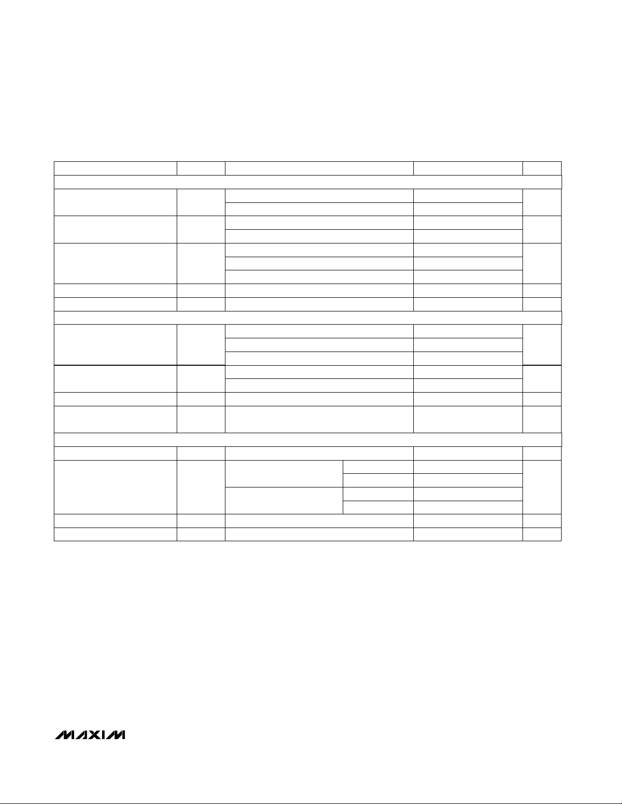
ELECTRICAL CHARACTERISTICS (continued)
(VDD= +3V to +3.6V, REF+ = 3V, REF- = GND, Read Mode (MODE = GND), TA= T
CONDITIONS
LOGIC INPUTS
Input High Voltage
Input Low Voltage
Input High Current
Input Low Current
Input Capacitance (Note 2)
LOGIC OUTPUTS
Output Low Voltage
Output High Voltage
Three-State Capacitance
(Note 2)
POWER REQUIREMENTS
Supply Voltage
VDDSupply Current
V
V
V
INH
INL
I
INH
INL
OL
OH
LKG
OUT
DD
I
DD
IN
CS, WR, RD, PWRDN, A0, A1, A2
MODE
CS, WR, RD, PWRDN, A0, A1, A2
MODE
CS, RD, PWRDN, A0, A1, A2
WR
MODE
CS, WR, RD, PWRDN, MODE, A0, A1, A2
CS, WR, RD, PWRDN, MODE, A0, A1, A2
I
= 20µA, INT, D0–D7
SINK
I
= 400µA, INT, D0–D7
SINK
RDY, I
I
SOURCE
I
SOURCE
D0–D7, RDY, digital outputs = 0V to V
D0–D7, RDY
VDD= 3.6V, CS = RD = 0V,
PWRDN = V
VDD= 3.0V, CS = RD = 0V,
PWRDN = V
CS = RD = VDD, PWRDN = 0V (Note 3)
VDD= 3.0V to 3.6V, V
= 1mA 0.4
SINK
= 20µA, INT, D0–D7
= 400µA, INT, D0–D7
MAX11_C
DD
DD
REF
MAX11_E/M
MAX11_C
MAX11_E/M
= 3.0V
MIN
DD
to T
, unless otherwise noted.)
MAX
2
2.4
VDD- 0.1
VDD- 0.4
0.66
0.8
±1
±3
15 100
0.1
±3Three-State Current
58
2.5 5
2.5 6
1.5 3
1.5 3.5
MAX113/MAX117
UNITSMIN TYP MAXSYMBOLPARAMETER
V
V
µA
µA±1I
pF58C
V0.4V
V
µAI
pFC
V3.0 3.6V
mA
µA110Power-Down VDDCurrent
LSB±1/16 ±1/4PSRPower-Supply Rejection
Note 1: Accuracy measurements performed at V
Note 2: Guaranteed by design.
Note 3: Power-down current increases if logic inputs are not driven to GND or V
_______________________________________________________________________________________ 3
= +3.0V. Operation over supply range is guaranteed by power-supply rejection test.
DD
DD
.
Page 4
+3V, 400ksps, 4/8-Channel,
8-Bit ADCs with 1µA Power-Down
TIMING CHARACTERISTICS
(VDD= +3V, TA= +25°C, unless otherwise noted.) (Note 4)
TA= +25°C
PARAMETER SYMBOL
Conversion Time
(WR-RD Mode)
Conversion Time
(RD Mode)
Power-Up Time t
CS to RD, WR
Setup Time
CS to RD, WR
Hold Time
MAX113/MAX117
CS to RDY Delay
Data Access Time
(RD Mode)
RD to INT Delay
(RD Mode)
Data Hold Time t
Minimum
Acquisition Time
WR Pulse Width
Delay Between WR
and RD Pulses
RD Pulse Width
(WR-RD Mode)
Data Access Time
(WR-RD Mode)
RD to INT Delay
WR to INT Delay
RD Pulse Width
(WR-RD Mode)
Data Access Time
(WR-RD Mode)
WR to INT Delay
Data Access Time
After INT
Multiplexer Address
Hold Time
t
CWR
t
CRD
UP
t
CSS
t
CSH
t
RDY
t
ACC0
t
INTH
DH
t
ACQ
t
WR
t
RD
t
READ1
t
ACC1
t
RI
t
INTL
t
READ2
t
ACC2
t
IHWR
t
ID
t
AH
tRD< t
(Note 5)
CL= 50pF,
= 5.1kΩ to V
R
L
CL= 100pF (Note 5)
CL= 50pF
(Note 6)
tRD< t
t
ACC1
tRD< t
(Note 5)
CL= 50pF
tRD> t
t
ACC2
tRD> t
(Note 5)
Pipelined mode, CL= 50pF
Pipelined mode, CL= 100pF
, CL= 100pF
INTL
DD
, determined by
INTL
, CL= 100pF
INTL
, determined by
INTL
, CL= 100pF
INTL
ALL GRADES
0 ns
0 ns
100 ns
t
CRD
100
100 160 ns
100 ns
450 ns(Note 7) 600
0.6 10 µs
0.8 µs
400 ns
400 ns
300 ns
0.7 1.45 µs
180 ns
180 ns
180 ns
100 ns
50 ns
TA= T
MIN MAX
1.8 µs
2.0 µs
0.9 µs
0
0
+
t
CRD
120
130
170
130
MIN
+
to T
MAX
MAX117M
MIN MAXMIN TYP MAX
0
0
t
CRD
2.42.06
2.62.4
1.41.2
140
150
180
150
UNITSCONDITIONS MAX117C/E
+
ns
700
0.8 100.66 10
500
340
1.6
220
200
130
1.0
600
600
400
1.8
250
250
240
150
70
0.9
500
220
60
Note 4: Input control signals are specified with t
delays get shorter at higher supply voltages. See the Conversion Time vs. Supply Voltage graph in the
Characteristics
to extrapolate timing delays at other power-supply voltages.
= tf= 5ns, 10% to 90% of 3V, and timed from a voltage level of 1.3V. Timing
r
Typical Operating
Note 5: See Figure 1 for load circuit. Parameter defined as the time required for the output to cross 0.66V or 2.0V.
Note 6: See Figure 2 for load circuit. Parameter defined as the time required for the data lines to change 0.5V.
Note 7: Also defined as the Minimum Address-Valid to Convert-Start Time.
4 _______________________________________________________________________________________
Page 5

+3V, 400ksps, 4/8-Channel,
8-Bit ADCs with 1µA Power-Down
__________________________________________Typical Operating Characteristics
(VDD= +3V, TA = +25°C, unless otherwise noted.)
CONVERSION TIME
vs. AMBIENT TEMPERATURE
1.6
1.4
1.2
VDD = 3.6V
1.0
= +3.3V, +25°C)
DD
0.8
(NORMALIZED TO VALUE
AT V
CRD
t
0.6
0.4
-60 140
VDD = 3.0V
-20 20 100
TEMPERATURE (°C)
1400
1300
1200
(ns)
1100
CRD
t
1000
900
60
MAX113/117-01
VDD = 3.3V
CONVERSION TIME
vs. SUPPLY VOLTAGE
INPUT FREQUENCY (WR-RD MODE)
8.0
7.5
7.0
6.5
6.0
5.5
EFFECTIVE BITS
5.0
f
4.5
SAMPLE
= 2.98Vp-p
V
IN
4.0
1k 10k 100k
MAX113/117-04
EFFECTIVE BITS vs.
= 400kHz
INPUT FREQUENCY (Hz)
5
4
3
2
POWER DISSIPATION (mW)
1
0
MAX113/117-02
-20
-40
SNR (dB)
-60
-80
-100
1M
40 80 160
0 200
AVERAGE POWER CONSUMPTION
vs. SAMPLING RATE USING PWRDN
SIGNAL-TO-NOISE RATIO
fIN = 30.27kHz
= 2.88Vp-p
V
IN
f
SAMPLE
SNR = 48.8dB
120
FREQUENCY (kHz)
MAX113/117-06
= 400ksps
MAX113/MAX117
MAX113/117-03
800
3.0 3.4 3.8
2.8 4.0
3.2
SUPPLY VOLTAGE (V)
3.6
0
1
10 100
SAMPLING RATE (ksps)
1000
TOTAL UNADJUSTED ERROR
vs. POWER-UP TIME
5
4
3
TUE (LSB)
2
1
0
VDD = 3.0V
VDD = 3.6V
120 160 240 320
200 280
tUP (ns)
MAX113/117-08
SUPPLY CURRENT vs. TEMPERATURE
(EXCLUDING REFERENCE CURRENT)
4
3
VDD = 3.3V
2
VDD = 3.0V
SUPPLY CURRENT (mA)
1
0
-60 140
TEMPERATURE (°C)
60 100-20 20
MAX113/117-10
V
DD
= 5.25V
_______________________________________________________________________________________
5
Page 6

+3V, 400ksps, 4/8-Channel,
8-Bit ADCs with 1µA Power-Down
______________________________________________________________Pin Description
PIN
MAX113
2 4
4 6
MAX113/MAX117
10
11
15
16
23
24
MAX117
1
3
5
7
8
9, 10, 11
12
13
14
15
16
17
18
19, 20, 21
22
23
24
25
26
27
28
NAME
IN3
IN1
MODE5
INT
REF-13
REF+14
WR/RDY
DD
FUNCTION
Analog Input Channel 6IN6—
Analog Input Channel 5IN5— 2
Analog Input Channel 4IN41
Analog Input Channel 3
Analog Input Channel 2IN23
Analog Input Channel 1
Mode Selection Input. Internally pulled low with a 15µA current source. MODE = 0
activates read mode; MODE = 1 activates write-read mode (see
section).
Three-State Data Output (LSB)D06
Three-State Data Outputs D1, D2, D37, 8, 9
Read Input. RD must be low to access data (see
Interrupt Output. INT goes low to indicate end of conversion (see
section).
GroundGND12
Lower limit of reference span. REF- sets the zero-code voltage. Range is GND ≤
V
< V
REF-
Upper limit of reference span. REF+ sets the full-scale input voltage. Range is
V
< V
REF-
Write-Control Input/Ready-Status Output (see
Chip-Select Input. CS must be low for the device to recognize WR or RD inputs.CS
Three-State Data Outputs D4, D5, D617, 18, 19
Three-State Data Output (MSB)D720
Multiplexer Channel Address Input (MSB)A2—
Multiplexer Channel Address Input A121
Multiplexer Channel Address Input (LSB)A022
Power-Down Input. PWRDN reduces supply current when low.PWRDN
Positive Supply, +3.0V to +3.6VV
Analog Input Channel 7IN7—
.
REF+
≤ VDD. Internally hardwired to IN8 (Table 1).
REF+
Digital Interface
Digital Interface
Digital Interface
section).RD
Digital Interface
section)
6 _______________________________________________________________________________________
Page 7

+3V, 400ksps, 4/8-Channel,
8-Bit ADCs with 1µA Power-Down
MAX113/MAX117
V
DD
= 3k
R
DATA
OUTPUTS
RL = 3k
a) HIGH-Z TO V
Figure 1. Load Circuits for Data-Access Time Test
OH
C
DATA
OUTPUTS
L
b) HIGH-Z TO V
L
C
L
OL
_______________Detailed Description
Converter Operation
The MAX113/MAX117 use a half-flash conversion technique (see
ADC sections achieve an 8-bit result. Using 15 comparators, the flash ADC compares the unknown input
voltage to the reference ladder and provides the upper
four data bits. An internal digital-to-analog converter
(DAC) uses the four most significant bits (MSBs) to
generate both the analog result from the first flash conversion and a residue voltage that is the difference
between the unknown input and the DAC voltage. The
residue is then compared again with the flash comparators to obtain the lower four data bits (LSBs).
An internal analog multiplexer enables the devices to
read four (MAX113) or eight (MAX117) different analog
voltages under microprocessor (µP) control. One of the
MAX117’s analog channels, IN8, is internally hardwired and always reads V
In burst-mode or low-sample-rate applications, the
MAX113/MAX117 can be shut down between conversions, reducing supply current to microamp levels (see
Typical Operating Characteristics
PWRDN pin shuts the devices down, reducing supply
current typically to 1µA when powered from a single
+3V supply. A logic high on PWRDN wakes up the
MAX113/MAX117, and the selected analog input enters
the track mode. The signal is fully acquired after 900ns
(this includes both the power-up delay and the
track/hold acquisition time), and a new conversion can
Functional Diagram
REF+
) in which two 4-bit flash
when selected.
Power-Down Mode
). A logic low on the
V
DD
TO HIGH-Z
OL
3k
10pF
DATA
OUTPUTS
3k
a) V
TO HIGH-Z b) V
OH
Figure 2. Load Circuits for Data-Hold Time Test
DATA
OUTPUTS
10pF
be started. If the power-down feature is not required,
connect PWRDN to VDD. For minimum current consumption, keep digital inputs at the supply rails in
power-down mode. Refer to the
Reference
section for
information on reducing the reference current during
power-down.
___________________Digital Interface
The MAX113/MAX117 have two basic interface modes,
which are set by the MODE pin. When MODE is low,
the converters are in read mode; when MODE is high,
the converters are set up for write-read mode. The A0,
A1, and A2 inputs control channel selection, as shown
in Table 1. The address must be valid for a minimum
time, t
Table 1. Truth Table for Input Channel
Selection
MAX113
00 IN1
10
11
——
——
——
——
, before the next conversion starts.
ACQ
MAX117
A2 A1 A0A1 A0
000
001
010
011
100
101
110
111
SELECTED CHANNEL
(reads V
IN201
IN3
IN4
IN5
IN6
IN7
IN8
REF+
if selected)
_______________________________________________________________________________________ 7
Page 8

+3V, 400ksps, 4/8-Channel,
8-Bit ADCs with 1µA Power-Down
Read Mode (MODE = 0)
In read mode, conversions and data access are controlled by the RD input (Figure 3). The comparator
inputs track the analog input voltage for the duration of
t
. A conversion is initiated by driving CS and RD
ACQ
low. With µPs that can be forced into a wait state, hold
RD low until output data appears. The µP starts the
conversion, waits, and then reads data with a single
read instruction.
In read mode, WR/RDY is configured as a status output
(RDY), so it can drive the ready or wait input of a µP.
RDY is an open-collector output (no internal pull-up)
that goes low after the falling edge of CS and goes high
at the end of the conversion. If not used, the WR/RDY
pin can be left unconnected. The INT output goes low
at the end of the conversion and returns high on the ris-
MAX113/MAX117
ing edge of CS or RD.
Write-Read Mode (MODE = 1)
Figures 4 and 5 show the operating sequence for writeread mode. The comparator inputs track the analog
input voltage for the duration of t
initiated by a falling edge of WR. When WR returns
high, the result of the four-MSBs flash is latched into the
output buffers and the conversion of the four-LSBs flash
starts. INT goes low, indicating conversion end, and the
lower four data bits are latched into the output buffers.
The data is then accessible after RD goes low (see
Timing Characteristics
A minimum acquisition time (t
).
ACQ
going low to the start of another conversion (WR going
low).
Options for reading data from the converter include
using internal delay, reading before delay, and pipelined
operation (discussed in the following sections).
. The conversion is
ACQ
) is required from INT
t
ADDRESS VALID
t
ACQ
t
RDY
UP
t
CSS
(N)
t
AH
WITH EXTERNAL
PULL-UP
t
CRD
t
ACCO
PWRDN
CS
RD
A0–A2
RDY
INT
D0–D7
Figure 3. Read Mode Timing (Mode = 0)
CS
t
CSH
t
WR
t
AH
t
CSS
t
RD
t
INTL
t
ACC2
WR
A0–A2
INT
D0–D7
t
CSS
t
ACQ
ADDRESS
VALID (N)
RD
Figure 4. Write-Read Mode Timing (tRD> t
t
CSH
t
ACQ
ADDRESS VALID (N + 1)
t
INTH
t
(N)
t
ACQ
t
READ2
VALID DATA
(N)
) (Mode = 1)
DH
t
DH
VALID DATA
ADDRESS VALID (N + 1)
INTL
t
t
CSH
AH
t
INTH
Using Internal Delay
The µP waits for the INT output to go low before reading
the data (Figure 4). INT goes low after the rising edge of
WR, indicating that the conversion is complete and the
result is available in the output latch. With CS low, data
outputs D0–D7 can be accessed by pulling RD low. INT
is then reset by the rising edge of CS or RD.
Fastest Conversion:
Reading Before Delay
An external method of controlling the conversion time is
shown in Figure 5. The internally generated delay
(t
) varies slightly with temperature and supply volt-
INTL
age, and can be overridden with RD to achieve the
fastest conversion time. RD is brought low after the rising edge of WR, but before INT goes low. This completes the conversion and enables the output buffers
CS
t
CSH
t
t
ACQ
ADDRESS
VALID (N)
WR
t
RD
t
CWR
t
INTL
t
t
ACC1
CSS
t
AH
WR
A0–A2
INT
D0–D7
t
CSS
RD
Figure 5. Write-Read Mode Timing (tRD< t
8 _______________________________________________________________________________________
t
ACQ
ADDRESS VALID (N + 1)
t
CSH
t
READ1
t
RI
t
VALID DATA
INTL
INTH
(N)
t
DH
) (Mode = 1)
Page 9

+3V, 400ksps, 4/8-Channel,
8-Bit ADCs with 1µA Power-Down
CS
t
CSS
RD, WR
t
ACQ
t
AH
A0–A2
INT
D0–D7
ADDRESS
VALID (N)
OLD DATA (N - 1)
Figure 6. Pipelined Mode Timing (WR = RD) (Mode = 1)
that contain the conversion result (D0–D7). INT also
goes low after the falling edge of RD and is reset on the
rising edge of RD or CS. The total conversion time is
therefore: tWR+ tRD+ t
Besides the two standard write-read-mode options,
“pipelined” operation can be achieved by connecting
WR and RD together (Figure 6). With CS low, driving
WR and RD low initiates a conversion and concurrently
reads the result of the previous conversion.
_____________Analog Considerations
Figures 7a, 7b, and 7c show typical reference connections. The voltages at REF+ and REF- set the ADC’s
analog input range (Figure 10). The voltage at REFdefines the input that produces an output code of all
zeros, and the voltage at REF+ defines the input that
produces an output code of all ones.
The internal resistance from REF+ to REF- can be as
low as 1kΩ, and current will flow through it even when
the MAX113/MAX117 are shut down. Figure 7d shows
how an N-channel MOSFET can be connected to REFto break this current path during power-down. The FET
should have an on-resistance of less than 2Ω with a 3V
gate drive. When REF- is switched, as in Figure 7d, a
new conversion can be initiated after waiting a time
equal to the power-up delay (tUP) plus the N-channel
FET’s turn-on time.
Although REF+ is frequently connected to VDD, the circuit of Figure 7d uses a low-current, low-dropout, 2.5V
voltage reference: the MAX872. Since the MAX872
cannot continuously furnish enough current for the ref-
t
CSH
t
WR
t
ACQ
ADDRESS
VALID (N + 1)
t
IHWR
t
INTL
t
ID
NEW DATA (N)
= 1800ns.
ACC1
Pipelined Operation
Reference
+3V
4.7µF
0.1µF
V
IN+
V
IN-
IN_
GND
V
REF+
REF-
DD
MAX113
MAX117
Figure 7a. Power Supply as Reference
V
IN+
V
IN-
IN_
GND
0.1µF
V
DD
REF+
REF-
MAX113
MAX117
+3V
4.7µF
0.1µF
7
6
8
1
3
LM10
4
2
+2.5V
34.8k
3.01k
Figure 7b. External Reference, 2.5V Full Scale
0.1µF
IN_
GND
V
DD
REF+
REF-
MAX113
MAX117
+3V
4.7µF
* CURRENT PATH MUST STILL
EXIST FROM V
0.1µF
TO GND
IN-
V
IN+
+2.5V
V
IN-
0.1µF
R*
Figure 7c. Input Not Referenced to GND
erence resistance, this circuit is intended for applications where the MAX113/MAX117 are normally in standby and are turned on in order to make measurements
at intervals greater than 100µs. C1 (the capacitor connected to REF+) is slowly charged by the MAX872 during the standby period, and furnishes the reference
current during the short measurement period.
The 4.7µF value of C1 ensures a voltage drop of less
than 1/2LSB when performing four to eight successive
conversions. Larger capacitors reduce the error still further. Use ceramic or tantalum capacitors for C1.
MAX113/MAX117
_______________________________________________________________________________________ 9
Page 10

+3V, 400ksps, 4/8-Channel,
8-Bit ADCs with 1µA Power-Down
+3V
0.1µF
V
DD
MAX113
REF+
MAX872
PWRDN
* IRML2402
Figure 7d. An N-channel MOSFET switches off the reference
MAX113/MAX117
load during power-down
N-FET*
C1
4.7µF
0.1µF
MAX117
REF-
PWRDN
Initial Power-Up
When power is first applied, perform a conversion to
initialize the MAX113/MAX117. Disregard the output
data.
Bypassing
Use a 4.7µF electrolytic in parallel with a 0.1µF ceramic
capacitor to bypass VDDto GND. Minimize capacitor
lead lengths.
Bypass the reference inputs with 0.1µF capacitors, as
shown in Figures 7a, 7b, and 7c.
MAX113
MUX
V
IN2
R
.
IN
.
.
MAX117
R
ON
Figure 8. Equivalent Input Circuit
R
V
IN_
1
2k
V
IN
22pF
T/H
10pF
MAX113
MAX117
Analog Inputs
Figure 9. RC Network Equivalent Input Model
Figure 8 shows the equivalent circuit of the MAX113/
MAX117 input. When a conversion starts and WR is
low, V
is connected to sixteen 0.6pF capacitors.
IN_
During this acquisition phase, the input capacitors
charge to the input voltage through the resistance of
the internal analog switches. In addition, about 22pF of
stray capacitance must be charged. The input can be
OUTPUT CODE
11111111
11111110
11111101
FULL-SCALE
TRANSITION
modeled as an equivalent RC network (Figure 9). As
source impedance increases, the capacitors take
longer to charge.
The typical 32pF input capacitance allows source resistance as high as 1.5kΩ without setup problems. For
larger resistances, the acquisition time (t
increased.
Internal protection diodes, which clamp the analog
input to VDDand GND, allow the channel input pins to
swing from GND - 0.3V to VDD+ 0.3V without damage.
However, for accurate conversions near full scale and
zero scale the inputs must not exceed VDDby more
than 50mV or be lower than GND by 50mV.
10 ______________________________________________________________________________________
ACQ
) must be
00000011
00000010
00000001
00000000
V
REF-
123
INPUT VOLTAGE (LSBs)
Figure 10. Transfer Function
1LSB =
FS - 1LSB
V
- V
REF+
REF-
256
V
REF+
FS
Page 11

+3V, 400ksps, 4/8-Channel,
8-Bit ADCs with 1µA Power-Down
If the analog input exceeds 50mV beyond the supplies, limit the input current to no more than two
milliamperes, as excessive current will degrade the
conversion accuracy of the on channel.
Track/Hold
The track/hold enters hold mode when a conversion
starts (RD low or WR low). INT goes low at the end of
the conversion, at which point the track/hold enters
track mode. The next conversion can start after the
minimum acquisition time, t
ACQ
.
Transfer Function
Figure 10 shows the MAX113/MAX117’s nominal transfer function. Code transitions occur halfway between
successive-integer LSB values. Output coding is binary
with 1LSB = (V
REF+
- V
REF-
) / 256.
Conversion Rate
The maximum sampling rate (f
MAX117 is achieved in write-read mode (tRD< t
and is calculated as follows:
f=
MAX
t + t + t + t
WR RD RI ACQ
f
=
MAX
f 465kHz
MAX
600ns 800ns 300ns 450ns
=
1
+++
where tWR= the write pulse width, tRD= the delay
between write and read pulses, tRI= RD to INT delay,
and t
= minimum acquisition time.
ACQ
) for the MAX113/
MAX
1
INTL
Signal-to-Noise Ratio and
Effective Number of Bits
Signal-to-noise plus distortion (SINAD) is the ratio of the
fundamental input frequency’s RMS amplitude to all
other ADC output signals. The output spectrum is limited to frequencies above DC and below one-half the
ADC sample rate.
The theoretical minimum analog-to-digital noise is
caused by quantization error, and results directly from
the ADC’s resolution: SNR = (6.02N + 1.76)dB, where
N is the number of bits of resolution. Therefore, a perfect 8-bit ADC can do no better than 50dB.
The FFT Plot (see
Typical Operating Characteristics
shows the result of sampling a pure 30.27kHz sinusoid
at a 400kHz rate. This FFT plot of the output shows the
output level in various spectral bands.
The effective resolution (or “effective number of bits”)
the ADC provides can be measured by transposing the
equation that converts resolution to SNR: N = (SINAD -
1.76) / 6.02 (see
Typical Operating Characteristics
Total Harmonic Distortion
Total harmonic distortion (THD) is the ratio of the RMS
sum of all harmonics of the input signal (in the frequency band above DC and below one-half the sample rate)
to the fundamental itself. This is expressed as:
)
2
242
+++
V V V ...V
2
THD = 20log
3
V
1
where V1is the fundamental RMS amplitude, and V
through VNare the amplitudes of the 2nd through Nth
harmonics.
Spurious-Free Dynamic Range
Spurious-free dynamic range (SFDR) is the ratio of the
fundamental RMS amplitude to the amplitude of the
next largest spectral component (in the frequency band
above DC and below one-half the sample rate). Usually
the next largest spectral component occurs at some
harmonic of the input frequency. However, if the ADC is
exceptionally linear, it may occur only at a random
peak in the ADC’s noise floor. See the Signal-to-Noise
Ratio graph in
Typical Operating Characteristics
N
2
MAX113/MAX117
)
).
2
.
______________________________________________________________________________________ 11
Page 12

+3V, 400ksps, 4/8-Channel,
8-Bit ADCs with 1µA Power-Down
__Ordering Information (continued)
PART
MAX117CPI
MAX117CAI
MAX117EPI
MAX117EAI
0°C to +70°C
0°C to +70°C
0°C to +70°CMAX117C/D
-40°C to +85°C
-55°C to +125°CMAX117MJI
PIN-PACKAGETEMP. RANGE
28 Wide Plastic DIP
28 SSOP
Dice*
28 Wide Plastic DIP-40°C to +85°C
28 SSOP
28 Wide CERDIP**
___________________Chip Information
TRANSISTOR COUNT: 2011
*Dice are specified at TA= +25°C, DC parameters only.
**Contact factory for availability.
MAX113/MAX117
__________________________________________________________Pin Configurations
TOP VIEW
IN4
IN3
IN2
IN1
MODE
INT
GND
IN6
1
2
3
4
MAX113
5
D0
6
D1
7
D2
8
D3
9
RD
10
11
12
24
23
22
21
20
19
18
17
16
15
14
13
V
DD
PWRDN
A0
A1
D7
D6
D5
D4
CS
WR/RDY
REF+
REF-
DIP/SSOP
IN5
IN4
IN3
IN2
IN1
MODE
INT
GND
1
2
3
4
5
MAX117
6
7
D0
8
D1
9
D2
10
D3
11
RD
12
13
14
28
27
26
25
24
23
22
21
20
19
18
17
16
15
IN7
V
DD
PWRDN
A0
A1
A2
D7
D6
D5
D4
CS
WR/RDY
REF+
REF-
DIP/SSOP
Maxim cannot assume responsibility for use of any circuitry other than circuitry entirely embodied in a Maxim product. No circuit patent licenses are
Maxim cannot assume responsibility for use of any circuitry other than circuitry entirely embodied in a Maxim product. No circuit patent licenses are
implied. Maxim reserves the right to change the circuitry and specifications without notice at any time.
implied. Maxim reserves the right to change the circuitry and specifications without notice at any time.
12
__________________Maxim Integrated Products, 120 San Gabriel Drive, Sunnyvale, CA 94086 (408) 737-7600
12
__________________Maxim Integrated Products, 120 San Gabriel Drive, Sunnyvale, CA 94086 (408) 737-7600
© 1996 Maxim Integrated Products Printed USA is a registered trademark of Maxim Integrated Products.
© 1996 Maxim Integrated Products Printed USA is a registered trademark of Maxim Integrated Products.
 Loading...