

Page 1
General Description
The MAX1142/MAX1143 are 200ksps, 14-bit ADCs.
These serially interfaced ADCs connect directly to
SPI™, QSPI™, and MICROWIRE™ devices without
external logic. They combine an input scaling network,
internal track/hold, a clock, +4.096V reference, and
three general-purpose digital output pins (for external
multiplexer or PGA control) in a 20-pin SSOP package.
The excellent dynamic performance (SINAD ≥ 81dB),
high-speed (200ksps), and low power (7.5mA) of these
ADCs, make them ideal for applications such as industrial process control, instrumentation, and medical
applications. The MAX1142 accepts input signals of 0
to +12V (unipolar) or ±12V (bipolar), while the
MAX1143 accepts input signals of 0 to +4.096V (unipolar) or ±4.096V (bipolar). Operating from a single
+4.75V to +5.25V analog supply and a +4.75V to
+5.25V digital supply, power-down modes reduce current consumption to 1mA at 10ksps and further reduce
supply current to less than 20µA at slower data rates.
A serial strobe output (SSTRB) allows direct connection
to the TMS320-family of digital signal processors. The
MAX1142/MAX1143 user can select either the internal
clock, or an external serial-interface clock for the ADC
to perform analog-to-digital conversions.
The MAX1142/MAX1143 feature internal calibration circuitry to correct linearity and offset errors. On-demand
calibration allows the user to optimize performance.
Three user-programmable logic outputs are provided
for the control of an 8-channel MUX or a PGA.
Applications
Industrial Process Control
Industrial I/O Modules
Data-Acquisition Systems
Medical Instruments
Portable and Battery-Powered Equipment
Features
♦ 200ksps (Bipolar) and 150ksps (Unipolar)
Sampling ADC
♦ 14-Bits, No Missing Codes
♦ 1LSB INL Guaranteed
♦ 81dB (min) SINAD
♦ +5V Single-Supply Operation
♦ Low Power Operation, 7.5mA (Unipolar Mode)
♦ 2.5µA Shutdown Mode
♦ Software-Configurable Unipolar & Bipolar Input
Ranges
0 to +12V and ±12V (MAX1142)
0 to +4.096V and ±4.096V (MAX1143)
Internal or External Reference
♦ Internal or External Clock
♦ SPI/QSPI/MICROWIRE-Compatible Wire Serial
Interface
♦ Three User-Programmable Logic Outputs
♦ Small 20-Pin SSOP Package
MAX1142/MAX1143
14-Bit ADC, 200ksps, +5V Single-Supply
with Reference
________________________________________________________________
Maxim Integrated Products
1
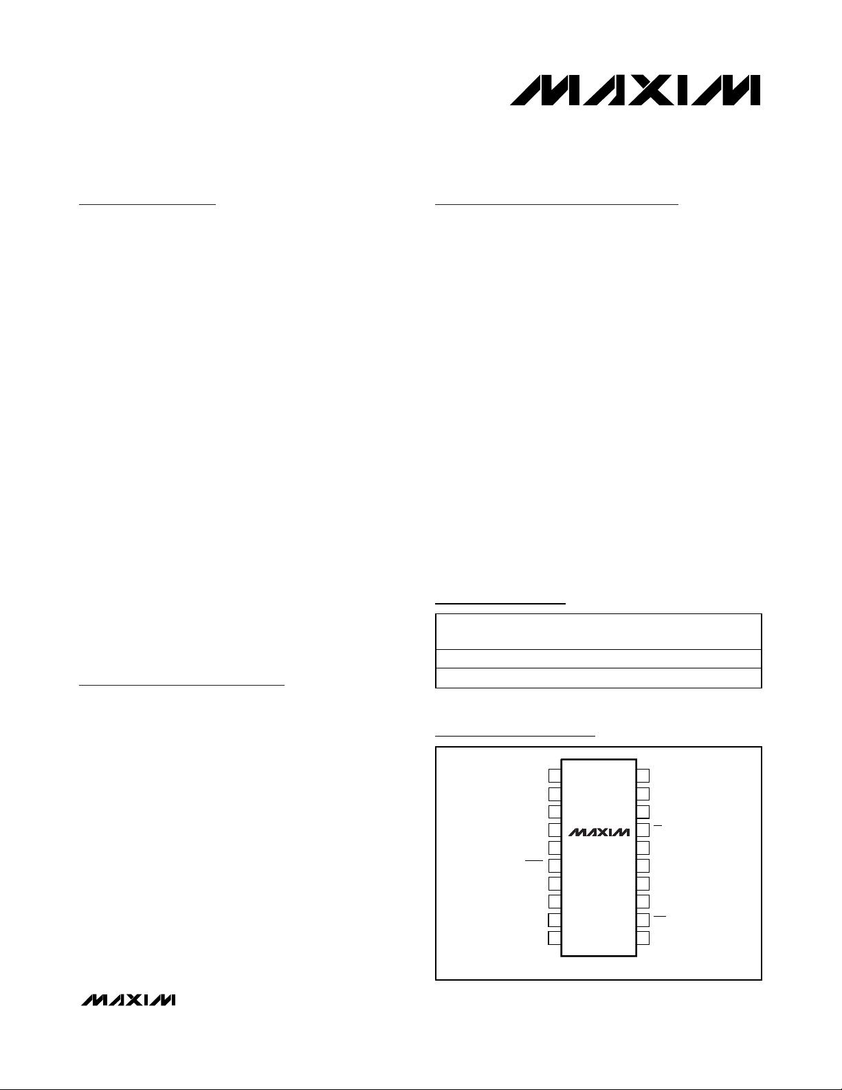
Pin Configuration
19-2037; Rev 0; 5/01
Ordering Information
Functional Diagram appears at end of data sheet.
Typical Application Circuit appears at end of data sheet.
SPI and QSPI are trademarks of Motorola, Inc.
MICROWIRE is a trademark of National Semiconductor Corp.
Ordering Information continued at end of data sheet.
For pricing, delivery, and ordering information, please contact Maxim/Dallas Direct! at
1-888-629-4642, or visit Maxim’s website at www.maxim-ic.com.
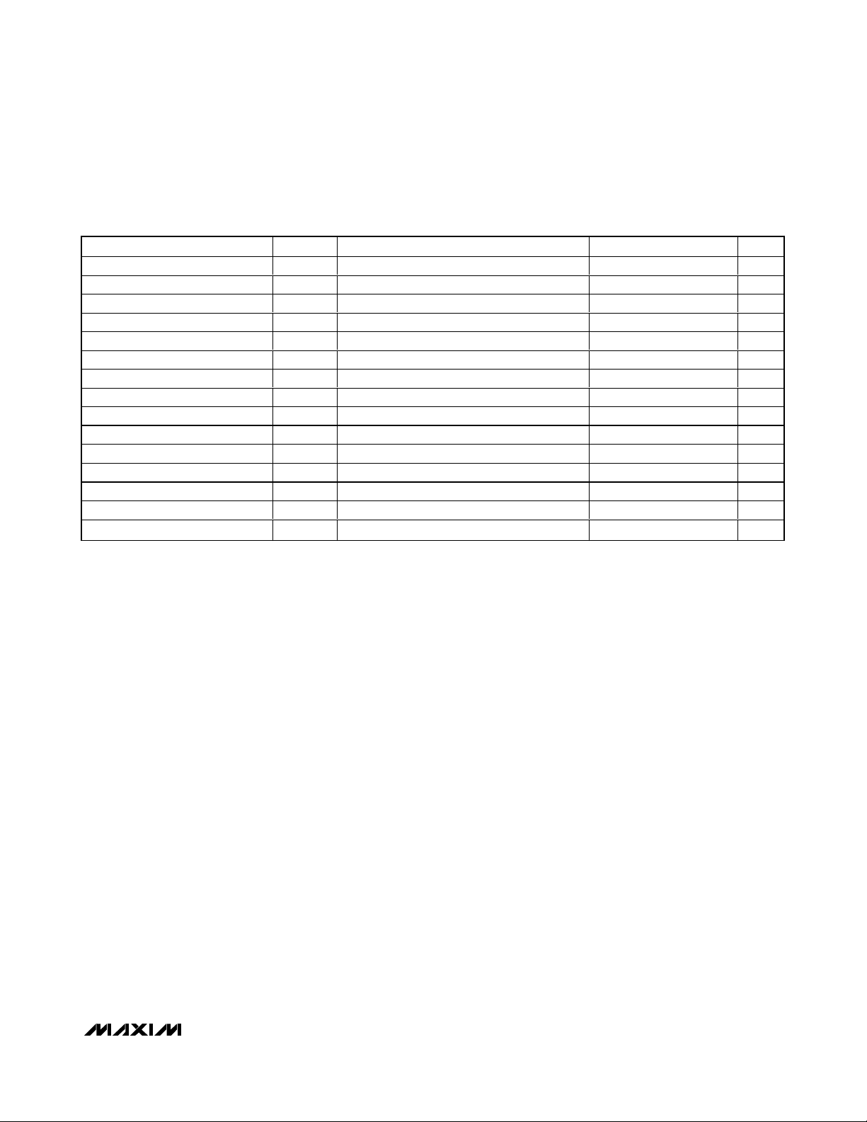
PART TEMP. RANGE
MAX1142ACAP 0°C to +70°C 20 SSOP ±1
MAX1142BCAP 0°C to +70°C 20 SSOP ±2
PIN-
PACKAGE
(LSB)
TOP VIEW
1
REF
2
REFADJ
3
AGND
4
AV
DD
DGND
SHDN
P2
P1
P0
SSTRB
MAX1142
5
MAX1143
6
7
8
9
10 DOUT
SSOP
20
AIN
19
AGND
CREF
18
17
CS
16
DIN
15
DV
DD
DGND
14
SCLK
13
12
RST
11
INL
Page 2
MAX1142/MAX1143
14-Bit ADC, 200ksps, +5V Single-Supply
with Reference
2 _______________________________________________________________________________________
ABSOLUTE MAXIMUM RATINGS
Stresses beyond those listed under “Absolute Maximum Ratings” may cause permanent damage to the device. These are stress ratings only, and functional
operation of the device at these or any other conditions beyond those indicated in the operational sections of the specifications is not implied. Exposure to
absolute maximum rating conditions for extended periods may affect device reliability.
AVDDto AGND, DVDDto DGND .............................-0.3V to +6V
AGND to DGND.....................................................-0.3V to +0.3V
AIN to AGND.....................................................................±16.5V
REFADJ, CREF, REF to AGND.................-0.3V to (AV
DD
+ 0.3V)
Digital Inputs to DGND.............................................-0.3V to +6V
Digital Outputs to DGND .........................-0.3V to (DV
DD
+ 0.3V)
Continuous Power Dissipation (T
A
= +70°C)
20-SSOP (derate 8.00mW/°C above +70°C) ...............640mW
Operating Temperature Ranges
MAX114_CAP ......................................................0°C to +70°C
MAX114_EAP....................................................-40°C to +85°C
Storage Temperature Range .............................-60°C to +150°C
Junction Temperature......................................................+150°C
Lead Temperature (soldering, 10s) .................................+300°C
ELECTRICAL CHARACTERISTICS
(AVDD= DVDD= +5V ±5%, f
SCLK
= 4.8MHz, external clock (50% duty cycle), 24 clocks/conversion (200ksps), bipolar input, external
V
REF
= +4.096V, V
REFADJ
= AVDD, C
REF
= 2.2µF, C
CREF
= 1µF, TA = T
MIN
to T
MAX
, unless otherwise noted. Typical values are at
T
A
= +25°C.)
PARAMETER SYMBOL CONDITIONS MIN TYP MAX UNITS
DC ACCURACY (Note 1)
Resolution 14 Bits
Relative Accuracy (Note 2) INL
Differential Nonlinearity DNL Unipolar Mode ±1 LSB
Transition Noise 0.34 LSB RMS
Offset Error
Gain Error (Note 3)
Offset D r i ft ( Bi p ol ar and U ni p ol ar ) Excluding reference drift ±1 ppm/
G ai n D r i ft ( Bi p ol ar and U ni p ol ar ) Excluding reference drift ±1 ppm/
DYNAMIC SPECIFICATIONS (5kHz sine-wave input, 200ksps, 4.8MHz clock, bipolar input mode).
(MAX1142, 24Vp-p. MAX1143, 8.192Vp-p)
SINAD
SNR
THD
SFDR
ANALOG INPUT
Input Range
Unipolar Mode MAX114_A ±1
Unipolar ±4
Bipolar ±6
Unipolar ±0.2
Bipolar ±0.3
f
= 5kHz 81
IN
f
= 100kHz 82
IN
f
= 5kHz 82
IN
f
= 100kHz 82
IN
f
= 5kHz -88
IN
f
= 100kHz 91
IN
f
= 5kHz 90
IN
f
= 100kHz 95
IN
MAX1142
MAX1143
MAX114_B ±2
Unipolar 0 12
Bipolar -12 12
Unipolar 0 4.096
Bipolar - 4.096 4.096
LSB
mV
%FSR
dB
dB
dB
dB
V
o
C
o
C
Page 3
MAX1142/MAX1143
14-Bit ADC, 200ksps, +5V Single-Supply
with Reference
_______________________________________________________________________________________ 3
ELECTRICAL CHARACTERISTICS (continued)
(AVDD= DVDD= +5V ±5%, f
SCLK
= 4.8MHz, external clock (50% duty cycle), 24 clocks/conversion (200ksps), bipolar input, external
V
REF
= +4.096V, V
REFADJ
= AVDD, C
REF
= 2.2µF, C
CREF
= 1µF, TA = T
MIN
to T
MAX
, unless otherwise noted. Typical values are at
T
A
= +25°C.)
PARAMETER SYMBOL CONDITIONS MIN TYP MAX UNITS
Input Impedance
Input Capacitance 32 pF
CONVERSION RATE
Internal Clock Frequency 4 MHz
Aperture Delay t
Aperture Jitter t
MODE 1 (24 External Clock Cycles per Conversion)
External Clock Frequency f
Sample Rate f
Conversion Time (Note 4)
MODE 2 (Internal Clock Mode)
External Clock Frequency
(Data Transfer Only)
Conversion Time SSTRB Low Pulse Width 4 6 µs
Acquisition Time
MODE 3 (32 External Clock Cycles per Conversion)
External Clock Frequency f
Sample Rate f
Conversion Time (Note 4)
INTERNAL REFERENCE
Output Voltage V
REF Short Circuit Current 24 mA
Output Tempco ±20 ppm/
Capacitive Bypass at REF 0.47 10 µF
Maximum Capacitive Bypass at
REFADJ
REFADJ Output Voltage 4.096 V
REFADJ Input Range For small adjustments from 4.096V ±100 mV
AD
AJ
SCLK
= f
S
t
CONV+ACQ
24 / f
/24
SCLK
=
SCLK Bipolar 5 240
MAX1142
MAX1143
Unipolar 7.5 10.0
Bipolar 5.9 7.9
Unipolar 100 1000
Bipolar 3.4 4.5
Unipolar 0.1 3
Bipolar 0.1 4.8
Unipolar 4.17 125
Bipolar 4.17 200
Unipolar 8 240
10 ns
50 ps
Unipolar 1.82
Bipolar 1.14
SCLK
= f
S
SCLK
t
CONV+ACQ
32 / f
SCLK
REF
Unipolar or Bipolar 0.1 4.8 MHz
/32 Unipolar or Bipolar 3.125 150 ksps
=
Unipolar or Bipolar 6.67 320 µs
4.056 4.096 4.136 V
10 µF
8 MHz
kΩ
MHz
ksps
µs
µs
o
C
Page 4
MAX1142/MAX1143
14-Bit ADC, 200ksps, +5V Single-Supply
with Reference
4 _______________________________________________________________________________________
ELECTRICAL CHARACTERISTICS (continued)
(AVDD= DVDD= +5V ±5%, f
SCLK
= 4.8MHz, external clock (50% duty cycle), 24 clocks/conversion (200ksps), bipolar input, external
V
REF
= +4.096V, V
REFADJ
= AVDD, C
REF
= 2.2µF, C
CREF
= 1µF, TA = T
MIN
to T
MAX
, unless otherwise noted. Typical values are at
T
A
= +25°C.)
PARAMETER SYMBOL CONDITIONS MIN TYP MAX UNITS
REFADJ Buffer Disable
Threshold
Buffer Voltage Gain 1 V/V
EXTERNAL REFERENCE (Reference buffer disabled. Reference applied to REF)
Input Range (Notes 5 and 6) 3.0 4.096 4.2 V
Input Current
DIGITAL INPUTS
Input High Voltage V
Input Low Voltage V
Input Leakage I
Input Hysteresis V
Input Capacitance C
DIGITAL OUTPUTS
Output High Voltage V
Output Low Voltage V
Three-State Leakage Current I
Three-State Output
Capacitance
POWER SUPPLIES
Analog Supply (Note 7) AV
Digital Supply (Note 7) DV
Analog Supply Current I
Digital Supply Current I
Power Supply Rejection Ratio
(Note 8)
IH
IL
IN
HYST
IN
OH
OL
L
DD
DD
To power-down the internal reference
V
= 4.096V, f
REF
V
= 4.096V, f
REF
In power-down, f
AVDD -
0.5V
= 4.8MHz 250
SCLK
= 0 230
SCLK
= 0 0.1
SCLK
2.4 V
VIN = 0 or DV
I
SOURCE
I
= 5mA 0.4
SINK
I
= 16mA 0.8
SINK
CS = DV
CS = DV
DD
= 0.5mA
DD
DD
DV
0.5
DD
-
4.75 5 5.25 V
4.75 5 5.25 V
0.2 V
10 pF
10 pF
Unipolar Mode 5 8
ANALOG
DIGITAL
PSRR AV
Bipolar Mode 8.5 11
SHDN = 0, or softw are power -down mode
0.3 10 µA
Unipolar or Bipolar Mode 2.5 3.5 mA
SHDN = 0, or softw are power -down mode
= DVDD = 4.75V to 5.25V, 72 dB
DD
2.2 10 µA
AVDD -
0.1V
0.8 V
±1 µA
±10 µA
V
µA
V
V
mA
Page 5
MAX1142/MAX1143
14-Bit ADC, 200ksps, +5V Single-Supply
with Reference
_______________________________________________________________________________________ 5
Note 1: Tested at AV
DD
= DV
DD
= +5V, bipolar input mode.
Note 2: Relative accuracy is the deviation of the analog value at any code from its theoretical value after the gain error and offset
error have been nulled.
Note 3: Offset nulled.
Note 4: Conversion time is defined as the number of clock cycles multiplied by the clock period, clock has 50% duty cycle.
Includes the acquisition time.
Note 5: ADC performance is limited by the converter’s noise floor, typically 300µVp-p.
Note 6 When an external reference has a different voltage than the specified typical value, the full scale of the ADC will scale
proportionally.
Note 7: Electrical characteristics are guaranteed from AV
DD(MIN)
= DV
DD(MIN)
to AV
DD(MAX)
= DV
DD(MAX)
. For operations beyond
this range, see the
Typical Operating Characteristics
. For guaranteed specifications beyond the limits, contact
the factory.
Note 8: Defined as the change in positive full-scale caused by a ±5% variation in the nominal supply voltage.
TIMING CHARACTERISTICS (Figures 5 and 6)
(AVDD= DVDD= +5V ±5%, TA= T
MIN
to T
MAX
, unless otherwise noted.)
Acquisition Time t
DIN to SCLK Setup t
DIN to SCLK Hold t
SCLK to DOUT Valid t
CS Fall to DOUT Enable t
CS Rise to DOUT Disable t
CS to SCLK Rise Setup t
CS to SCLK Rise Hold t
SCLK High Pulse Width t
SCLK Low Pulse Width t
SCLK Fall to SSTRB t
CS Fall to SSTRB Enable t
CS Rise to SSTRB Disable t
SSTRB Rise to SCLK Rise t
RST Pulse Width t
PARAMETER SYMBOL CONDITIONS MIN TYP MAX UNIT
ACQ
DS
DH
DO
DV
TR
CSS
CSH
CH
CL
SSTRB
SDV
STR
SCK
RS
C
LOAD
C
LOAD
C
LOAD
C
LOAD
C
LOAD
Internal clock mode 0 ns
1.14 µs
50 ns
0 ns
70 ns
= 50pF 80 ns
= 50pF 80 ns
100 ns
0 ns
80 ns
80 ns
= 50pF 80 ns
= 50pF, External clock mode 80 ns
= 50pF, External clock mode 80 ns
208 ns
Page 6
MAX1142/MAX1143
14-Bit ADC, 200ksps, +5V Single-Supply
with Reference
6 _______________________________________________________________________________________
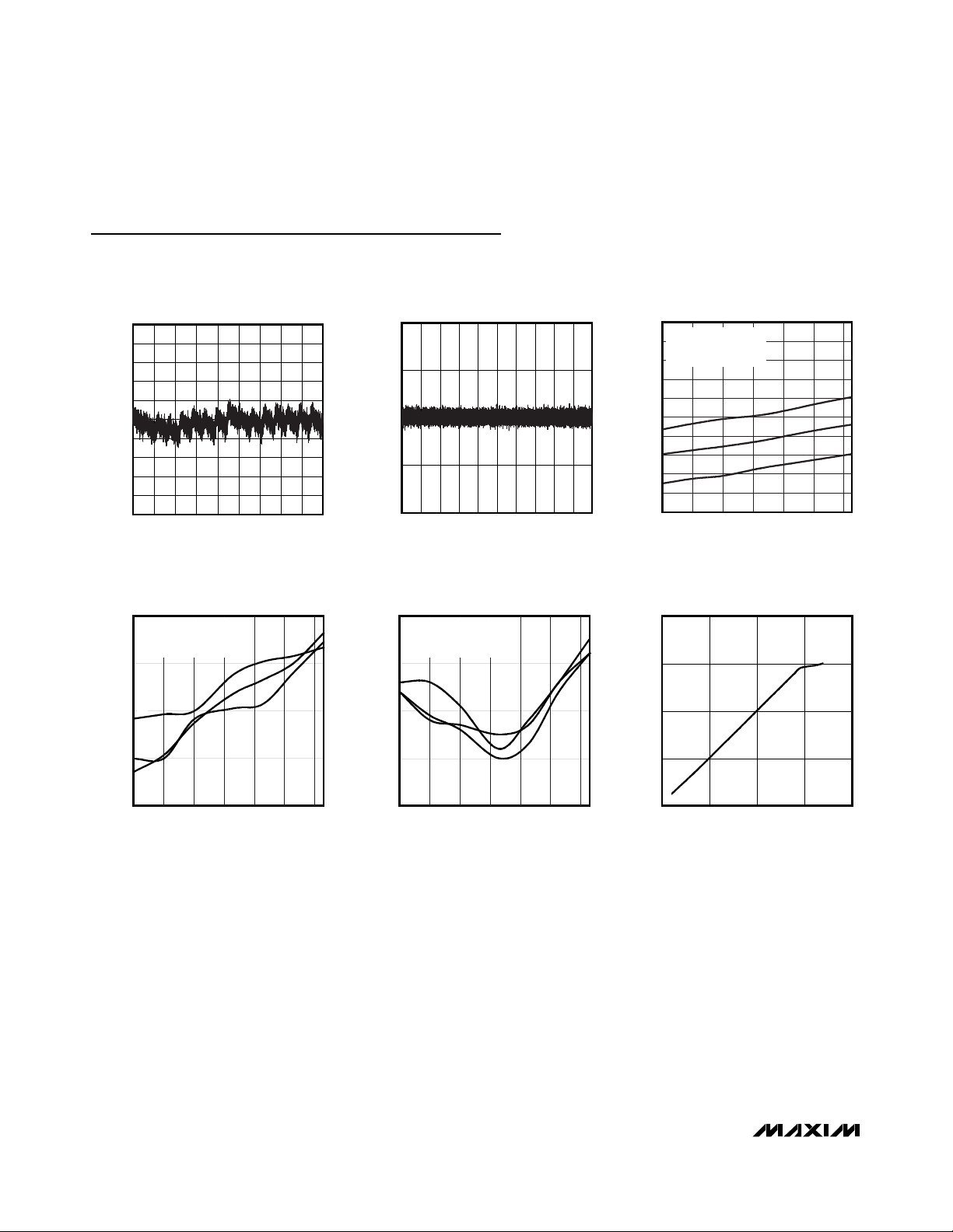
Typical Operating Characteristics
(MAX1142/MAX1143, AVDD= DVDD= +5V , f
SCLK
= 4.8MHz, external clock (50% duty cycle), 24-clocks/conversion (200ksps), bipo-
lar input, external REF = +4.096V, 0.22µF bypassing on REFADJ, 2.2µF on REF, 1µF on CREF, TA= 25°C, unless otherwise noted.)
-1.0
-0.6
-0.8
-0.2
-0.4
0.2
0
0.4
0.8
0.6
1.0
1 3433
5149
6865
1717 8581
10297
12013
13729
15445
INTEGRAL NONLINEARITY
vs. DIGITAL OUTPUT CODE
MAX1142 toc01
DIGITAL OUTPUT CODE
INTEGRAL NONLINEARITY (LSB)
-1.0
-0.5
0.5
0
1.0
1 3263
4894
6525
81561632
9787
11418
13049
14680
1631
DIFFERENTIAL NONLINEARITY
vs. DIGITAL OUTPUT CODE
MAX1142 toc02
DIGITAL OUTPUT CODE
DIFFERENTIAL NONLINEARITY (LSB)
9.5
10.1
9.9
9.7
10.5
10.3
11.3
11.1
10.9
10.7
11.5
-40 -20 0 20 40 60 80
TOTAL SUPPLY CURRENT
vs. TEMPERATURE
MAX1142/3 toc03
TEMPERATURE (°C)
TOTAL SUPPLY CURRENT (mA)
A: AVDD, DVDD = +4.75V
B: AVDD, DVDD = +5.00V
C: AVDD, DVDD = +5.25V
C
B
A
-4
0
-1
-2
-3
OFFSET VOLTAGE
vs. TEMPERATURE
MAX1142/3 toc04
TEMPERATURE (°C)
OFFSET VOLTAGE (V)
-40 20 40-20 0 60 80
A: AVDD, DVDD = +4.75V
B: AV
DD
, DVDD = +5.00V
C: AV
DD
, DVDD = +5.25V
A
B
C
GAIN ERROR vs.
TEMPERATURE
MAX1142/3 toc05
GAIN ERROR (% FULL SCALE)
0
0.04
0.03
0.02
0.01
TEMPERATURE (°C)
-40 20 40-20 0 60 80
A: AVDD, DVDD = +4.75V
B: AV
DD
, DVDD = +5.00V
C: AV
DD
, DVDD = +5.25V
A
B
C
0.01
0.1
1
10
100
TOTAL SUPPLY CURRENT vs.
CONVERSION RATE (USING SHUTDOWN)
MAX1142/3 toc06
CONVERSION RATE (ksps)
TOTAL SUPPLY CURRENT (mA)
0 100 10001 10
Page 7
MAX1142/MAX1143
14-Bit ADC, 200ksps, +5V Single-Supply
with Reference
_______________________________________________________________________________________
7
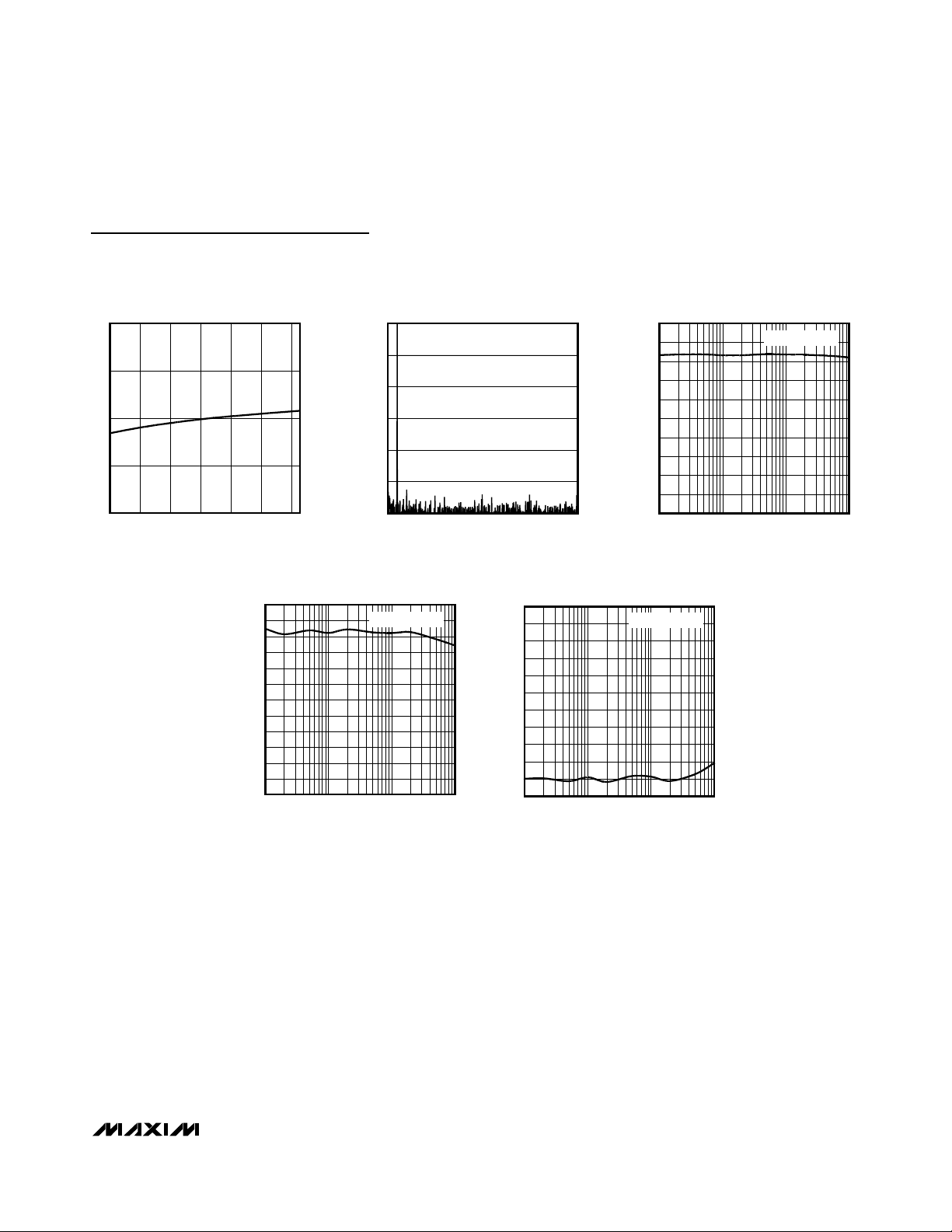
Typical Operating Characteristics (continued)
(MAX1142/MAX1143, AVDD= DVDD= +5V , f
SCLK
= 4.8MHz, external clock (50% duty cycle), 24-clocks/conversion (200ksps), bipo-
lar input, external REF = +4.096V, 0.22µF bypassing on REFADJ, 2.2µF on REF, 1µF on CREF, TA= 25°C, unless otherwise noted.)
1.010
1.005
1
0.995
0.990
-40 400 60-20 20 80
NORMALIZED REF VOLTAGE
vs. TEMPERATURE
MAX1142/3 toc07
TEMPERATURE (°C)
NORMALIZED REF VOLTAGE
-120
-110
-80
-40
-60
-20
0
0 189 27 36 45 54 63 72 81 90 99
FFT PLOT
MAX1142/3 toc08
FREQUENCY (kHz)
AMPLITUDE (dB)
f
SAMPLE
= 200kHz
f
IN
= 5kHz
MAX1142/3 toc09
0
20
10
30
40
60
50
90
80
70
100
0.1 1 10 100
SINAD PLOT
FREQUENCY (kHz)
AMPLITUDE (dB)
f
SAMPLE
= 200kHz
SFDR PLOT
120
110
100
90
80
70
60
50
AMPLITUDE (dB)
40
30
20
10
0
0.1 1 10 100
FREQUENCY (kHz)
THD PLOT
f
SAMPLE
= 200kHz
MAX1142/3 toc10
0
-10
-20
-30
-40
-50
-60
-70
AMPLITUDE (dB)
-80
-90
-100
-110
0.1 1 10 100
FREQUENCY (kHz)
f
SAMPLE
= 200kHz
MAX1142/3 toc11
Page 8

MAX1142/MAX1143
14-Bit ADC, 200ksps, +5V Single-Supply
with Reference
8 _______________________________________________________________________________________
Pin Description
PIN NAME FUNCTION
Reference Buffer Output/ADC Reference Input. Reference voltage for analog-to-digital conversion. In
1 REF
internal reference mode, the reference buffer provides a +4.096V nominal output, externally adjustable at
REFADJ. In external reference mode, disable the internal buffer by pulling REFADJ to AV
AGND with a 2.2µF capacitor when using the internal reference.
. Bypass to
DD
2 REFADJ
3 AGND Analog Ground. This is the primary analog ground (Star Ground).
4 AV
5 DGND Digital Ground
6 SHDN Shutdown Control Input. Drive SHDN low to put the ADC in shutdown mode.
7 P2 User-Programmable Output 2
8 P1 User-Programmable Output 1
9 P0 User-Programmable Output 0
10 SSTRB
11 DOUT
12 RST Reset Inp ut. D r i ve RST l ow to p ut the d evi ce i n the p ow er - on d efaul t m od e. S ee the
13 SCLK
14 DGND Digital Ground. Connect to pin 5.
15 DV
16 DIN Serial Data Input. Serial data on DIN is latched on the rising edge of SCLK.
17 CS
18 CREF Reference Buffer Bypass. Bypass CREF to AGND (pin 3) with 1µF.
DD
DD
Bandgap Reference Output/Bandgap Reference Buffer Input. Bypass to AGND with 0.22µF. When using an
external reference, connect REFADJ to AV
Analog Supply 5V ±5%. Bypass AV
Serial Strobe Output. In internal clock mode, SSTRB goes low when the ADC begins a conversion and goes
high when the conversion is finished. In external clock mode, SSTRB pulses high for one clock period
before the MSB decision. It is high impedance when CS is high in external clock mode.
Serial Data Output. MSB first, straight binary format for unipolar input, two’s complement for bipolar input.
Each bit is clocked out of DOUT at the falling edge of SCLK.
Serial Data Clock Input. Serial data on DIN is loaded on the rising edge of SCLK, and serial data is updated
on DOUT on the falling edge of SCLK. In external clock mode, SCLK sets the conversion speed.
Digital Supply 5V ±5%. Bypass DV
Chip Select Input. Drive CS low to enable the serial interface. When CS is high, DOUT is high-impedance.
In external clock mode SSTRB is high-impedance when CS is high.
to disable the internal bandgap reference.
DD
to AGND (pin 3) with a 0.1µF capacitor.
DD
to DGND (pin 14) with a 0.1µF capacitor.
DD
P ow er - O n Reset
secti on.
19 AGND Analog Ground. Connect pin 19 to pin 3.
20 AIN Analog Input
Page 9
MAX1142/MAX1143
14-Bit ADC, 200ksps, +5V Single-Supply
with Reference
_______________________________________________________________________________________ 9
Detailed Description
The MAX1142/MAX1143 analog-to-digital converters
(ADCs) use a successive-approximation technique and
input track/hold (T/H) circuitry to convert an analog signal
to a 14-bit digital output. The MAX1142/MAX1143 easily
interfaces to microprocessors (µPs). The data bits can be
read either during the conversion in external clock mode
or after the conversion in internal clock mode.
In addition to a 14-bit ADC, the MAX1142/MAX1143
include an input scaler, an internal digital microcontroller,
calibration circuitry, an internal clock generator, and an
internal bandgap reference. The input scaler for the
MAX1142 enables conversion of input signals ranging
from 0 to +12V (unipolar input) or ±12V (bipolar input).
The MAX1143 accepts 0 to +4.096V (unipolar input) or
±4.096V (bipolar input). Input range selection is software
controlled.
Calibration
To minimize linearity, offset, and gain errors, the
MAX1142/MAX1143 have on-demand software calibration. Initiate calibration by writing a Control-Byte with bit
M1 = 0, and bit M0 = 1 (See Table 1). Select internal or
external clock for calibration by setting the INT/EXT bit in
the Control-Byte. Calibrate the MAX1142/MAX1143 with
the clock used for performing conversions.
Offsets resulting from synchronous noise (such as the
conversion clock) are canceled by the MAX1142/
MAX1143’s calibration circuitry. However, because the
magnitude of the offset produced by a synchronous signal depends on the signal’s shape, recalibration may be
appropriate if the shape or relative timing of the clock or
other digital signals change, as might occur if more than
one clock signal or frequency is used.
Input Scaler
The MAX1142/MAX1143 have an input scaler which
allows conversion of true bipolar input voltages while
operating from a single +5V supply. The input scaler
attenuates and shifts the input, as necessary, to map the
external input range to the input range of the internal
DAC. The MAX1142 analog input range is 0 to +12V
(unipolar) or ±12V (bipolar). The MAX1143 analog input
range is 0 to +4.096V (unipolar) or ±4.096V (bipolar).
Unipolar and bipolar mode selection is configured with bit
6 of the serial Control-Byte.
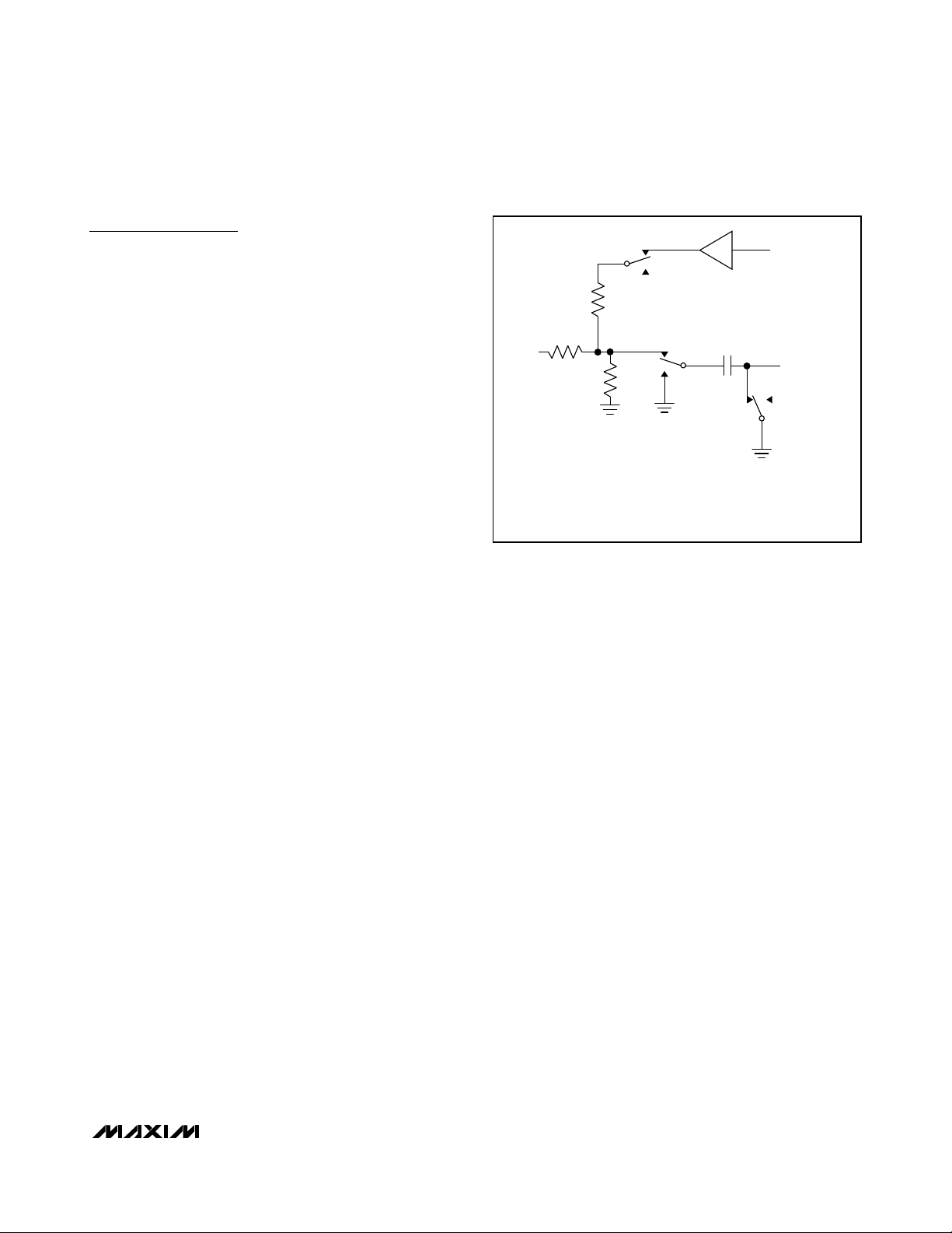
Figure 1 shows the equivalent input circuit of the
MAX1142/MAX1143. The resistor network on the analog
input provides ±16.5V fault protection. This circuit limits
the current going into or out of the pin, to less than 2mA.
The overvoltage protection is active, even if the device is
in a power-down mode, or if AVDD= 0.
Digital Interface
The digital interface pins consist of SHDN, RST, SSTRB,
DOUT, SCLK, DIN and CS. Bringing SHDN low, places
the MAX1142/MAX1143 in its 2.5µA shutdown mode. A
logic low on RST halts the MAX1142/MAX1143 operation and returns the part to its power-on reset state.
In external clock mode, SSTRB is low and pulses high
for one clock cycle at the start of conversion. In internal
clock mode SSTRB goes low at the start of the conversion, and goes high to indicate the conversion is finished.
The DIN input accepts Control-Byte data which is
clocked in on each rising edge of SCLK. After CS goes
low or after a conversion or calibration completes, the
first logic “1” clocked-into DIN is interpreted as the
START bit, the MSB of the 8-bit Control-Byte.
The SCLK input is the serial data transfer clock which
clocks data in and out of the MAX1142/MAX1143.
SCLK also drives the A/D conversion steps in external
clock mode (see
Internal and External Clock Modes
section).
DOUT is the serial output of the conversion result.
DOUT is updated on the falling edge of SCLK. DOUT is
high-impedance when CS is high.
CS must be low for the MAX1142/MAX1143 to accept a
Control-Byte. The serial interface is disabled when CS
is high.
Figure 1. Equivalent Input Circuit
BIPOLAR
S1
UNIPOLAR
R1
2.5kΩ
R2
AIN
S1 = BIPOLAR/UNIPOLAR
S2, S3 = T/H SWITCH
TRACK
R3
C
HOLD
30pF
S2
HOLD
TRACK
R2 = 7.6kΩ (MAX1142)
OR 2.5kΩ (MAX1143)
R3 = 3.9kΩ (MAX1142)
OR INFINITY (MAX1143)
VOLTAGE
REFERENCE
T/H OUT
HOLD
S3
Page 10

MAX1142/MAX1143
14-Bit ADC, 200ksps, +5V Single-Supply
with Reference
10 ______________________________________________________________________________________
User-Programmable Outputs
The MAX1142/MAX1143 have three user-programmable outputs: P0, P1 and P2. The power-on default state
for the programmable outputs is zero. These are pushpull CMOS outputs suitable for driving a multiplexer, a
PGA, or other signal preconditioning circuitry. The userprogrammable outputs are controlled by bits 0, 1 and 2
of the Control-Byte (Table 2).
The user-programmable outputs are set to zero during
power-on reset (POR) or when RST goes low. During
hardware or software shutdown P0, P1, and P2 are
unchanged and remain low-impedance.
Starting a Conversion
Start a conversion by clocking a Control-Byte into the
device’s internal shift register. With CS low, each rising
edge on SCLK clocks a bit from DIN into the
MAX1142/MAX1143’s internal shift register. After CS
goes low or after a conversion or calibration completes,
the first arriving logic “1” is defined as the start bit of
the Control-Byte. Until this first start bit arrives, any
number of logic “0” bits can be clocked into DIN with
no effect. If at any time during acquisition or conversion,
CS is brought high and then low again, the part is
placed into a state where it can recognize a new start
bit. If a new start bit occurs before the current conversion is complete, the conversion is aborted and a new
acquisition is initiated. Table 1 shows the Control-Byte
format.
Internal and External Clock Modes
The MAX1142/MAX1143 may use either the external
serial clock or the internal clock to perform the successive-approximation conversion. In both clock modes,
the external clock shifts data in and out of the
MAX1142/MAX1143. Bit 5 (INT/EXT) of the Control-Byte
programs the clock mode.
External Clock
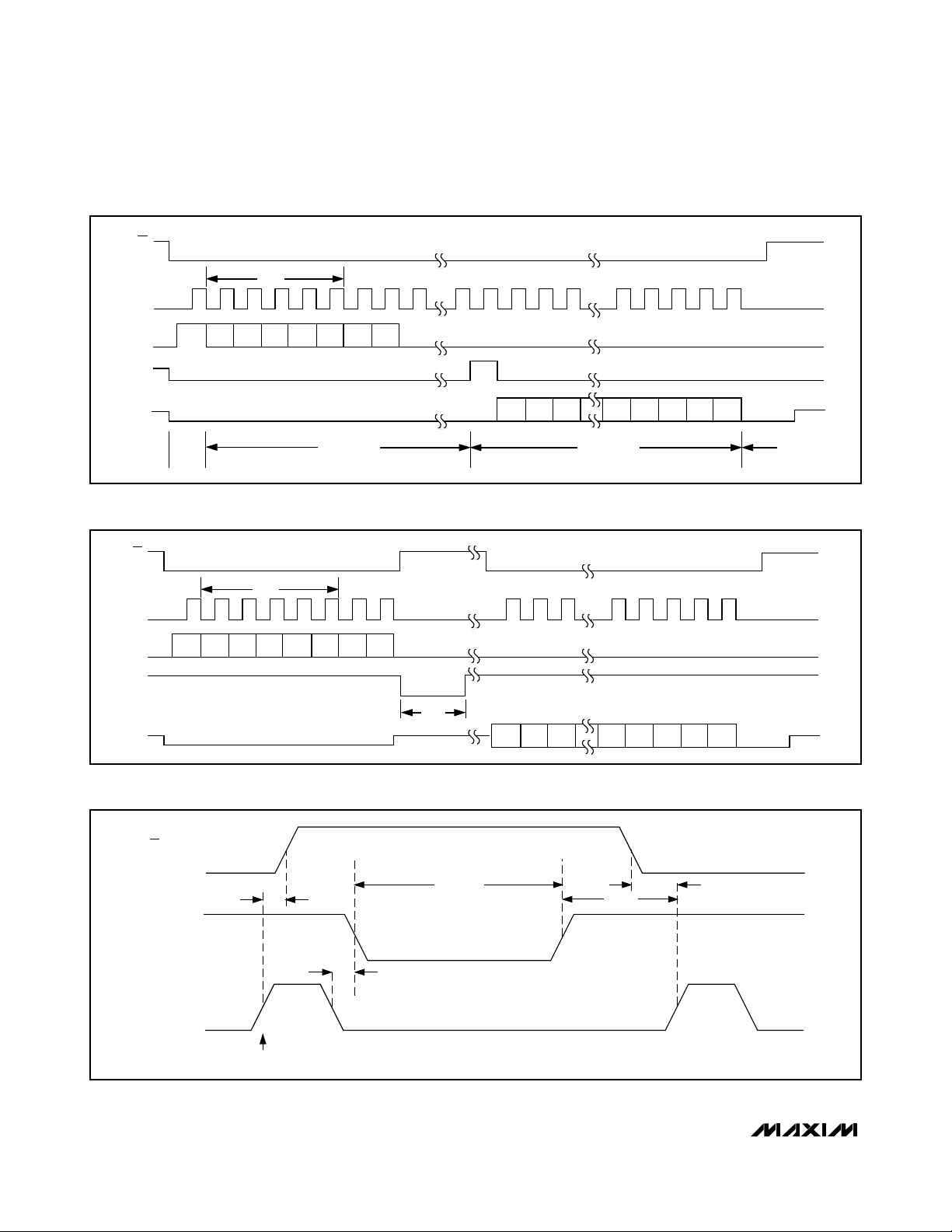
In external clock mode, the external clock not only
shifts data in and out, but it also drives the A/D conversion steps. In short acquisition mode, SSTRB pulses
high for one clock period after the seventh falling edge
of SCLK, following the start bit. The MSB of the conversion is available at DOUT on the eighth falling edge of
SCLK (Figure 2).
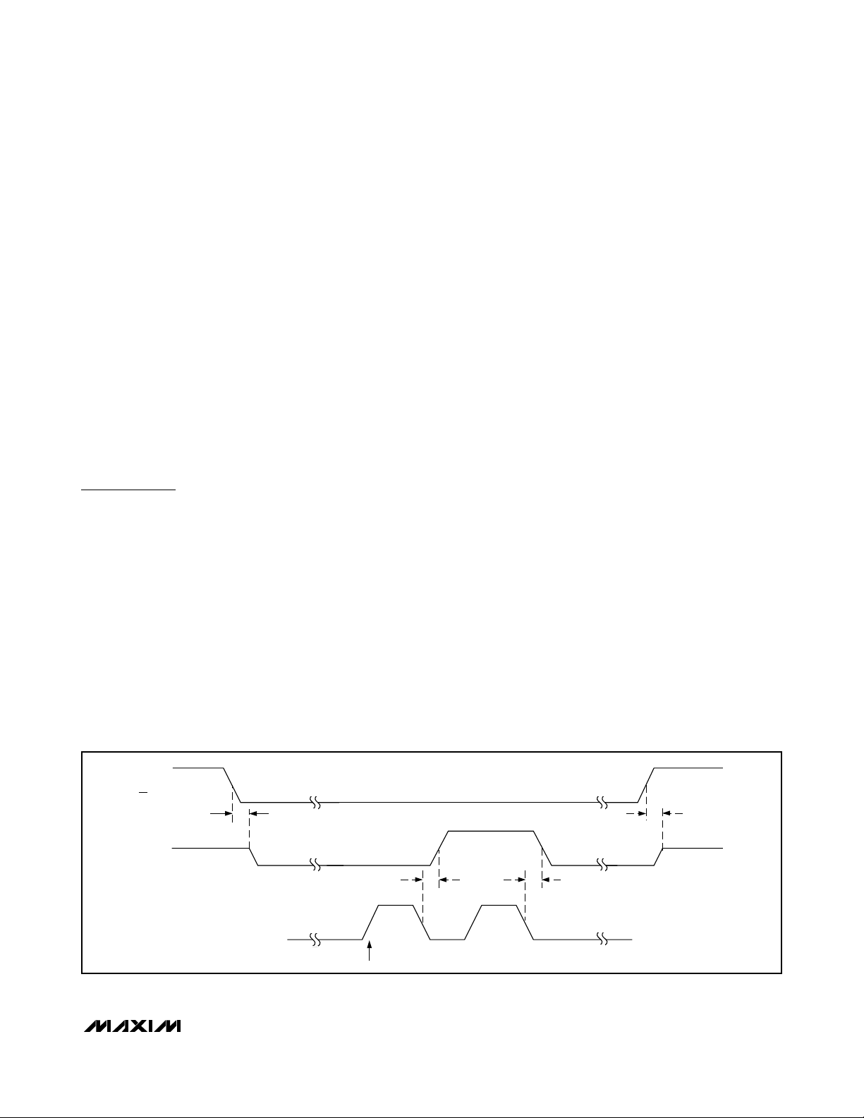
In long acquisition mode, when using the external
clock, SSTRB pulses high for one clock period after the
fifteenth falling edge of SCLK, following the start bit.
The MSB of the conversion is available at DOUT on the
sixteenth falling edge of SCLK (Figure 3).
Table 1. Control-Byte Format
BIT7
(MSB)
START UNI/BIP INT/EXT M1 M0 P2 P1 P0
BIT NAME DESCRIPTION
7 (MSB) START The first logic “1” bit, after CS goes low, defines the beginning of the Control-Byte
6 UNI/BIP
5 INT/EXT Selects the internal or external conversion clock. 1 = Internal, 0 = External.
4 M1 M1 M0 MODE
3 M0
2
1
0(LSB)
BIT6 BIT5 BIT4 BIT3 BIT2 BIT1
1 = unipolar, 0 = bipolar. Selects unipolar or bipolar conversion mode. In unipolar mode, analog
(MAX1143) can be converted. In bipolar
REF
REF
to +V
REF
P2
P1
P0
input signals from 0 to +12V (MAX1142) or 0 to V
mode analog input signals from -12V to +12V (MAX1142) or -V
converted.
0 0 24 External clocks per conversion (short acquisition mode)
0 1 Start Calibration. Starts internal calibration
1 0 Software power-down mode
1 1 32 External clocks per conversion (long acquisition mode)
These three bits are stored in a port register and output to pins P2–P0 for use in addressing a
MUX or PGA. These three bits are updated in the port register simultaneously when a new
Control-Byte is written.
(MAX1143) can be
BIT0
(LSB)
Page 11

MAX1142/MAX1143
14-Bit ADC, 200ksps, +5V Single-Supply
with Reference
______________________________________________________________________________________ 11
In external clock mode, SSTRB is high-impedance
when CS is high. In external clock mode, CS is normally
held low during the entire conversion. If CS goes high
during the conversion, SCLK is ignored until CS goes
low. This allows external clock mode to be used with 8bit bytes.
Internal Clock
In internal clock mode, the MAX1142/MAX1143 generates its own conversion clock. This frees the microprocessor from the burden of running the SAR conversion clock, and allows the conversion results to be read
back at the processor’s convenience, at any clock rate
up to 8MHz.
SSTRB goes low at the start of the conversion and goes
high when the conversion is complete. SSTRB will be
low for a maximum of 6µs, during which time SCLK
should remain low for best noise performance. An internal register stores data when the conversion is in
progress. SCLK clocks the data out of the internal storage register at any time after the conversion is complete.
The MSB of the conversion is available at DOUT when
SSTRB goes high. The subsequent 15 falling edges on
SCLK shift the remaining bits out of the internal storage
register (Figure 4). CS does not need to be held low
once a conversion is started.
When internal clock mode is selected, SSTRB does not
go into a high-impedance state when CS goes high.
Figure 5 shows the SSTRB timing in internal clock
mode. In internal clock mode, data can be shifted into
the MAX1142/MAX1143 at clock rates up to 4.8MHz,
provided that the minimum acquisition time,
t
ACQ
, is kept above 1.14µs in bipolar mode and 1.82µs
in unipolar-mode. Data can be clocked out at 8MHz.
Output Data
The output data format is straight binary for unipolar
conversions and two’s complement in bipolar mode. In
both modes the MSB is shifted out of the MAX1142/
MAX1143 first.
Table 2. User-Programmable Outputs
Figure 2. Short Acquisition Mode (24-Clock Cycles) External Clock, Bipolar Mode
OUTPUT
PIN
P2 Bit 2 0
P1 Bit 1 0
P0 Bit 0 0
PROGRAMMED
THROUGH
CONTROL-
BYTE
CS
POWER-ON
OR RST
DEFAULT
U ser p r og r am m ab l e outp uts fol l ow the state of the C ontr ol - Byte’ s thr ee LS Bs,
and ar e up d ated si m ul taneousl y w hen a new C ontr ol - Byte i s w r i tten. O utp uts
ar e p ush- p ul l . In har d w ar e and softw ar e shutd ow n, these outp uts ar e
unchang ed and r em ai n l ow - i m p ed ance.
DESCRIPTION
t
ACQ
SCLK
UNI/
START
DIN
SSTRB
DOUT
A/D
STATE
BIP
41 8 12
INT/
M1 M0
EXT
ACQUISITION CONVERSIONIDLE IDLE
P2
P1 P0
B13
MSB
B10 B9B12 B11
B8
15
B7 B2
21 24
B0
B1 X X
LSB
FILLED WITH
ZEROS
Page 12
MAX1142/MAX1143
14-Bit ADC, 200ksps, +5V Single-Supply
with Reference
12 ______________________________________________________________________________________
Figure 3. Long Acquisition Mode (32-Clock Cycles) External Clock, Bipolar Mode
Figure 4. Internal Clock Mode Timing, Short Acquisition, Bipolar Mode
Figure 5. Internal Clock Mode SSTRB Detailed Timing
CS
t
ACQ
SCLK
DIN
SSTRB
START
UNI/
BIP
41 8 19
INT/
EXT
M1 M0
P2
P1 P0
15
21 32
DOUT
A/D
STATE
ACQUISITION CONVERSIONIDLE IDLE
SCLK
DIN
SSTRB
DOUT
CS
t
ACQ
41 8
UNI/
START
BIP
INT/
EXT
M1 M0
P2
P1 P0
t
CONV
B13
MSB
CS
B13
MSB
X X
FILLED WITH
ZEROS
FILLED WITH
ZEROS
B11
9
B2B12
B2B12 B11
B0
B1
LSB
2110 24
B0
B1
LSB
X X
SSTRB
SCLK
PO CLOCKED IN
t
t
CSH
t
SSTRB
CONV
NOTE: FOR BEST NOISE PERFORMANCE, KEEP SCLK LOW DURING CONVERSION.
t
SCK
t
CSS
Page 13
MAX1142/MAX1143
14-Bit ADC, 200ksps, +5V Single-Supply
with Reference
______________________________________________________________________________________ 13
Data Framing
The falling edge of CS does NOT start a conversion on
the MAX1142/MAX1143. The first logic high clocked
into DIN is interpreted as a start bit and defines the first
bit of the Control-Byte. A conversion starts on the falling
edge of SCLK, after the seventh bit of the Control-Byte
(the P1 bit) is clocked into DIN. The start bit is defined
as:
The first high bit clocked into DIN with CS low, anytime the converter is idle, e.g. after AVDDis applied,
or as the first high bit clocked into DIN after CS is
pulsed high, then low.
OR
If a falling edge on CS forces a start bit before the
conversion or calibration is complete, then the current operation will be terminated and a new one
started.
Applications Information
Power-On Reset
When power is first applied to the MAX1142/MAX1143
or if RST is pulsed low, the internal calibration registers
are set to their default values. The user-programmable
registers (P0, P1 and P2) are low, and the device is
configured for bipolar mode with internal clocking.
Calibration
To compensate the MAX1142/MAX1143 for temperature drift and other variations, they should be periodically calibrated. After any change in ambient
temperature more than 10°C, the device should be
recalibrated. A 100mV change in supply voltage or any
change in the reference voltage should be followed by
a calibration. Calibration corrects for errors in gain, offset, integral nonlinearity and differential nonlinearity.
The MAX1142/MAX1143 should be calibrated after
power-up or the assertion of reset. Make sure the
power supplies and the reference voltage have fully
settled prior to initiating the calibration sequence.
Initiate calibration by setting M1 = 0 and M0 = 1 in the
Control-Byte. In internal clock mode, SSTRB goes low
at the beginning of calibration and goes high to signal
the end of calibration, approximately 80,000 clock
cycles later. In external clock mode, SSTRB goes high
at the beginning of calibration and goes low to signal
the end of calibration. Calibration should be performed
in the same clock mode as will be used for conversions
(Figure 6).
Reference
The MAX1142/MAX1143 can be used with an internal or
external reference. An external reference can be connected directly at the REF pin or at the REFADJ pin.
CREF is an internal reference node and must be
bypassed with a 1µF capacitor when using either the
internal or an external reference.
Internal Reference
When using the MAX1142/MAX1143’s internal reference, place a 0.22µF ceramic capacitor from REFADJ
to AGND and place a 2.2µF capacitor from REF to
AGND. Fine adjustments can be made to the internal
reference voltage by sinking or sourcing current at
REFADJ. The input impedance of REFADJ is nominally
9kΩ. The internal reference voltage is adjustable to
±1.5% with the circuit of Figure 7.
Figure 6. External Clock Mode SSTRB Detailed Timing
CS
t
SDV
SSTRB
SCLK
P1 CLOCKED IN
t
SSTRB
t
SSTRB
t
STR
Page 14

MAX1142/MAX1143
14-Bit ADC, 200ksps, +5V Single-Supply
with Reference
14 ______________________________________________________________________________________
External reference
An external reference can be placed at either the input
(REFADJ) or the output (REF) of the MAX1142/
MAX1143’s internal buffer amplifier.
When connecting an external reference to REFADJ, the
input impedance is typically 9kΩ. Using the buffered
REFADJ input makes buffering of the external reference
unnecessary. The internal buffer output must be
bypassed at REF with a 2.2µF capacitor.
When connecting an external reference at REF,
REFADJ must be connected to AVDD. The input imped-
ance at REF is 16kΩ for DC currents. During conver-
sion, an external reference at REF must deliver 250µA
DC load current and have an output impedance of 10Ω
or less. If the reference has a higher output impedance
or is noisy, bypass it at the REF pin with a 4.7µF capacitor.
Analog Input
The MAX1142/MAX1143 use a capacitive DAC that
provides an inherent track/hold function. Drive AIN with
a source impedance less than 10Ω. Any signal condi-
tioning circuitry must settle with 16-bit accuracy in less
than 500ns. Limit the input bandwidth to less than half
the sampling frequency to eliminate aliasing. The
MAX1142/MAX1143 has a complex input impedance
which varies from unipolar to bipolar mode (Figure 1).
Input Range
The analog input range in unipolar mode is 0 to +12V
for the MAX1142, and 0 to +4.096V for the MAX1143. In
bipolar mode, the analog input can be -12V to +12V for
the MAX1142, and -4.096V to +4.096V for the
MAX1143. Unipolar and bipolar mode is programmed
with the UNI/BIP bit of the Control-Byte. When using a
reference other than the MAX1142/MAX1143’s internal
+4.096V reference, the full-scale input range will vary
accordingly. The full-scale input range depends on the
voltage at REF and the sampling mode selected (Tables
3 and 4).
Input Acquisition and Settling
Clocking-in a Control-Byte starts input acquisition. In
bipolar mode, the main capacitor array starts acquiring
the input as soon as a start bit is recognized. If unipolar
mode is selected by the second DIN bit, the part will
immediately switch to unipolar sampling mode and
acquire a sample.
Acquisition can be extended by eight clock cycles by
setting M1 = 1, M0 = 1 (long acquisition mode). The
sampling instant in short acquisition completes on the
falling edge of the sixth clock cycle after the start bit
(Figure 2).
Figure 7. MAX1142 Reference-Adjust Circuit
Table 3. Unipolar Full Scale and Zero Scale
Table 4. Bipolar Full Scale, Zero Scale, and Negative Scale
PART REFERENCE ZERO SCALE FULL SCALE
MAX1142
MAX1143
Internal 0 +12V
External 0 +12(V
Internal 0 +4.096V
External 0 +V
+5V
510kΩ
100kΩ
24kΩ
0.22µF
MAX1142
REFADJ
/4.096)
REF
REF
PART REFERENCE
MAX1142
MAX1143
Internal -12V 0 +12V
External -12(V
Internal -4.096V 0 +4.096V
External -V
NEGATIVE FULL
SCALE
/4.096) 0 +12(V
REF
REF
ZERO SCALE FULL SCALE
0 +V
REF
/4.096)
REF
Page 15

MAX1142/MAX1143
14-Bit ADC, 200ksps, +5V Single-Supply
with Reference
______________________________________________________________________________________ 15
Acquisition is 5.5 clock cycles in short acquisition
mode and 13.5 clock cycles in long acquisition mode.
Short acquisition mode is 24 clock cycles per conversion. Using the external clock to run the conversion
process limits unipolar conversion speed to 125ksps
instead of 200ksps in bipolar mode. The input resistance in unipolar mode is larger than that of bipolar
mode (Figure1). The RC time constant in unipolar mode
is larger than that of bipolar mode, reducing the maximum conversion rate in 24 external clock mode. Long
acquisition mode with external clock allows both unipolar and bipolar sampling of 150ksps (4.8MHz/32 clock
cycles) by adding eight extra clock cycles to the conversion.
Most applications require an input buffer amplifier. If
the input signal is multiplexed, the input channel should
be switched immediately after acquision, rather than
near the end of or after a conversion. This allows more
time for the input buffer amplifier to respond to a large
step change in input signal. The input amplifier must
have a high enough slew-rate to complete the required
output voltage change before the beginning of the
acquisition time. At the beginning of acquisition, the
capacitive DAC is connected to the amplifier output,
causing some output disturbance. Ensure that the sampled voltage has settled to within the required limits
before the end of the acquisition time. If the frequency
of interest is low, AIN can be bypassed with a large
enough capacitor to charge the capacitive DAC with
very little change in voltage. However, for AC use, AIN
must be driven by a wideband buffer (at least 10MHz),
which must be stable with the DAC’s capacitive load (in
parallel with any AIN bypass capacitor used) and also
settle quickly (Figures 8 or 9).
Digital Noise
Digital noise can couple to AIN and REF. The conversion clock (SCLK) and other digital signals that are
active during input acquisition, contribute noise to the
conversion result. If the noise signal is synchronous to
the sampling interval, an effective input offset is produced. Asynchronous signals produce random noise
on the input, whose high-frequency components may
be aliased into the frequency band of interest. Minimize
noise by presenting a low impedance (at the frequencies contained in the noise signal) at the inputs. This
requires bypassing AIN to AGND, or buffering the input
with an amplifier that has a small-signal bandwidth of
several MHz, or preferably both. AIN has a bandwidth
of about 4MHz.
Figure 8. AIN Buffer for AC/DC Use
Figure 9. ±5V Buffer for AC/DC Use has ±3.5V Swing
1kΩ
510Ω
+5V
0.1µF
2
MAX410
3
IN
-5V
7
6
4
0.1µF
22Ω
AIN
0.1µF
+15V
2
MAX427
3
IN
7
4
-15V
0.1µF
6
0.1µF
1000pF
AIN
20Ω
0.0033µF
Page 16

MAX1142/MAX1143
14-Bit ADC, 200ksps, +5V Single-Supply
with Reference
16 ______________________________________________________________________________________
Offsets resulting from synchronous noise (such as the
conversion clock) are canceled by the MAX1142/
MAX1143’s calibration scheme. The magnitude of the
offset produced by a synchronous signal depends on
the signal’s shape. Recalibration may be appropriate if
the shape or relative timing of the clock or other digital
signals change, as might occur if more than one clock
signal or frequency is used.
Distortion
Avoid degrading dynamic performance by choosing an
amplifier with distortion much less than the MAX1142/
MAX1143’s THD (-88dB) at frequencies of interest. If
the chosen amplifier has insufficient common-mode
rejection, which results in degraded THD performance,
use the inverting configuration to eliminate errors from
common-mode voltage. Low temperature-coefficient
resistors reduce linearity errors caused by resistance
changes due to self-heating. To reduce linearity errors
due to finite amplifier gain, use an amplifier circuit with
sufficient loop gain at the frequencies of interest.
DC Accuracy
If DC accuracy is important, choose a buffer with an
offset much less than the MAX1142/MAX1143’s maximum offset (±6mV), or whose offset can be trimmed
while maintaining good stability over the required temperature range.
Operating Modes and Serial Interfaces
The MAX1142/MAX1143 are fully compatible with
MICROWIRE and SPI/QSPI devices. MICROWIRE and
SPI/QSPI both transmit a byte and receive a byte at the
same time. The simple software interface requires only
three 8-bit transfers to perform a conversion, one 8-bit
transfer to configure the ADC, and two more 8-bit transfers to clock out the 14-bit conversion result.
Mode 1 Short Acquisition Mode (24 SCLK)
Configure short acquisition by setting M1 = 0 and M0 =
0. In short acquisition mode, the acquisition time is 5.5
clock cycles. The total period is 24-clock cycles per
conversion.
Mode 2 Long Acquisition Mode (32 SCLK)
Configure long acquisition by setting M1 = 1 and M0 =
1. In long acquisition mode, the acquisition time is 13.5
clock cycles. The total period is 32 clock cycles per
conversion.
Calibration Mode
A calibration is initiated through the serial interface by
setting M1 = 0, M0 = 1. Calibration can be done in
either internal or external clock mode, though it is desirable that the part be calibrated in the same mode in
which it will be used to do conversions. The part will
remain in calibration mode for approximately 80,000
clock cycles, unless the calibration is aborted.
Calibration is halted if RST or SHDN goes low, or if a
valid start condition occurs.
Software Shut-Down
A software power-down is initiated by setting M1 = 1,
M0 = 0. After the conversion completes, the part shuts
down. It reawakens upon receiving a new start bit.
Conversions initiated with M1 = 1 and M0 = 0 (shutdown) use the acquisition mode selected for the previous conversion.
Shutdown Mode
The MAX1142/MAX1143 may be shut down by pulling
SHDN low or by asserting software shutdown. In addition to lowering power dissipation to 13µW, considerable power can be saved by shutting down the
converter for short periods between conversions.
Duration will be affected by REF startup time with internal reference. There is no need to perform a calibration
after the converter has been shut down, unless the time
in shutdown is long enough that the supply voltage or
ambient temperature may have changed.
Supplies, Layout, Grounding
and Bypassing
For best system performance, use separate analog and
digital ground planes. The two ground planes should
be tied together at the MAX1142/MAX1143. Use pins 3
and 14 as the primary AGND and DGND, respectively.
If the analog and digital supplies come from the same
source, isolate the digital supply from the analog with a
low value resistor (10Ω).
The MAX1142/MAX1143 are not sensitive to the order
of AVDDand DVDDsequencing. Either supply can be
present in the absence of the other. Do not apply an
external reference voltage until after both AV
DD
and
DVDDare present.
Be sure that digital return currents do not pass through
the analog ground. All return current paths must be
low-impedance. A 5mA current flowing through a PC
board ground trace impedance of only 0.05Ω, creates
an error voltage of about 250µV, or about 2LSBs error
with a ±4V full-scale system. The board layout should
ensure that the digital and analog signal lines are kept
separate. Do not run analog and digital lines parallel to
one another. If you must cross one with the other, do so
at right angles.
The ADC is sensitive to high-frequency noise on the
AVDDpower supply. Bypass this supply to the analog
ground plane with 0.1µF. If the main supply is not ade-
Page 17
MAX1142/MAX1143
14-Bit ADC, 200ksps, +5V Single-Supply
with Reference
___________________________________________________ 17
quately bypassed, add an additional 1µF or 10µF lowESR capacitor in parallel with the primary bypass
capacitor.
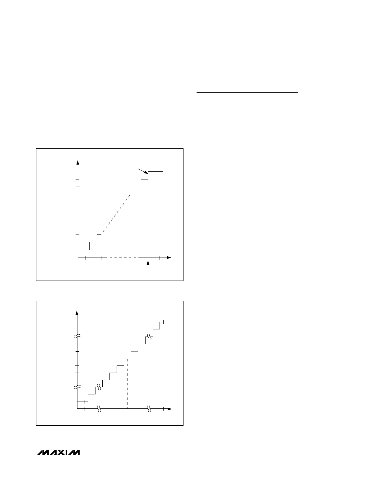
Transfer Function
Figures 10 and 11 show the MAX1142/MAX1143’s
transfer functions. In unipolar mode, the output data is
in binary format and in bipolar mode, it is two’s complement format.
Definitions
Integral Nonlinearity
Integral nonlinearity (INL) is the deviation of the values
on an actual transfer function from a straight line. This
straight-line can be either a best straight-line fit or a line
drawn between the end points of the transfer function,
once offset and gain errors have been nullified. INL for
the MAX1142/MAX1143 is measured using the endpoint method.
Differential Nonlinearity
Differential nonlinearity (DNL) is the difference between
an actual step width and the ideal value of 1LSB. A
DNL error specification of less than 1LSB guarantees
no missing codes and a monotonic transfer function.
Aperture Jitter
Aperture jitter (tAJ) is the sample-to-sample variation in
the time between the samples.
Aperture Delay
Aperture delay (tAD) is the time between the rising
edge of the sampling clock and the instant when an
actual sample is taken.
Signal-to-Noise Ratio
For a waveform perfectly reconstructed from digital
samples, signal-to-noise ratio (SNR) is the ratio of fullscale analog input (RMS value) to the RMS quantization
error (residual error). The ideal, theoretical, minimum
analog-to-digital noise is caused by quantization error
only and results directly from the ADC’s resolution
(N-bits):
SNR = (6.02 ✕N + 1.76)dB
In reality, there are other noise sources besides quantization noise, including thermal noise, reference noise,
clock jitter, etc. Therefore, SNR is calculated by taking
the ratio of the RMS signal to the RMS noise, which
includes all spectral components minus the fundamental, the first five harmonics and the DC offset.
Signal-to-Noise Plus Distortion
Signal-to-noise plus distortion (SINAD) is the ratio of the
fundamental input frequency’s RMS amplitude to the
RMS equivalent of all other ADC output signals:
SINAD (dB) = 20 ✕log (Signal
RMS
/Noise
RMS
)
Figure 10. MAX1143 Unipolar Transfer Function, 4.096V = FullScale
Figure 11. MAX1143 Bipolar Transfer Function, 4.096V = FullScale
OUTPUT CODE
FULL-SCALE
11 . . . 111
11 . . . 110
11 . . . 101
00 . . . 011
00 . . . 010
00 . . . 001
00 . . . 000
011 . . . 111
011 . . . 110
000 . . . 010
000 . . . 001
000 . . . 000
111 . . . 111
111 . . . 110
111 . . . 101
100 . . . 001
100 . . . 000
0
OUTPUT CODE
+FS = +4.096V
-FS = -4.096V
1LSB = 8.192
12 3
INPUT VOLTAGE (LSBs)
16384
TRANSITION
FS = +4.096V
FS - 3/2LSB
1LSB = FS
16384
FS
-FS
0V
INPUT VOLTAGE (LSBs)
+FS - 1LSB
Page 18

Effective Number of Bits
Effective number of bits (ENOB) indicates the global
accuracy of an ADC at a specific input frequency and
sampling rate. An ideal ADC’s error consists of quantization noise only. With an input range equal to the fullscale range of the ADC, calculate the effective number
of bits as follows:
ENOB = (SINAD - 1.76) / 6.02
Total Harmonic Distortion
Total harmonic distortion (THD) is the ratio of the RMS
sum of the first five harmonics of the input signal to the
fundamental itself. This is expressed as:
where V1is the fundamental amplitude, and V2through
V5are the amplitudes of the 2nd- through 5th-order
harmonics.
Spurious-Free Dynamic Range
Spurious-free dynamic range (SFDR) is the ratio of RMS
amplitude of the fundamental (maximum signal component), to the RMS value of the next largest distortion
component.
Chip Information
TRANSISTOR COUNT: 21,807
PROCESS : BiCMOS
MAX1142/MAX1143
14-Bit ADC, 200ksps, +5V Single-Supply
with Reference
18 ______________________________________________________________________________________
Ordering Information (continued)
Typical Application Circuit
*Future product—contact factory for availability.
2
THD = × + + +
20
log /V V V V V
2
2
3
425
+5V
0.1µF
AV
DD
SHDN
+5V
MAX1142
MAX1143
AIN
2
1
1µF
CREF
REF
REFADJ
0.22µF2.2µF
DGND AGND
DV
DD
0.1µF
TO DGND
CS
SCLK SCLK
DIN
DOUT
RST
SSTRB
I/O
MOSI
MISO
I/O
MC68HCXX
PART TEMP. RANGE
MAX1142AEAP -40°C to +85°C 20 SSOP ±1
MAX1142BEAP -40°C to +85°C 20 SSOP ±2
MAX1143ACAP* 0°C to +70°C 20 SSOP ±1
MAX1143BCAP* 0°C to +70°C 20 SSOP ±2
MAX1143AEAP* -40°C to +85°C 20 SSOP ±1
MAX1143BEAP* -40°C to +85°C 20 SSOP ±2
PIN-
PACKAGE
INL
(LSB)
Page 19

MAX1142/MAX1143
14-Bit ADC, 200ksps, +5V Single-Supply
with Reference
______________________________________________________________________________________ 19
Functional Diagram
CREF
AV
DD
9kΩ
AGND
REFADJ
REF
CS
RST
REFERENCE
AIN
DV
DD
DGND
SCLK
DIN
ANALOG TIMING CONTROL
INPUT
SCALING
NETWORK
SERIAL
OUTPUT
PORT
SERIAL
INPUT
PORT
MEMORY CALIBRATION
ENGINE
CLOCK
GENERATOR
CONTROL
DAC
COMPARATOR
P2
SSTRB
DOUT
P1
P0
SHDN
MAX1142
MAX1143
Page 20

MAX1142/MAX1143
14-Bit ADC, 200ksps, +5V Single-Supply
with Reference
Maxim cannot assume responsibility for use of any circuitry other than circuitry entirely embodied in a Maxim product. No circuit patent licenses are
implied. Maxim reserves the right to change the circuitry and specifications without notice at any time.
20
____________________Maxim Integrated Products, 120 San Gabriel Drive, Sunnyvale, CA 94086 408-737-7600
© 2001 Maxim Integrated Products Printed USA is a registered trademark of Maxim Integrated Products.
Package Information
SSOP.EPS
 Loading...