

Page 1
General Description
The MAX1127 quad, 12-bit analog-to-digital converter
(ADC) features fully differential inputs, a pipelined
architecture, and digital error correction. This ADC is
optimized for low-power, high-dynamic performance for
medical imaging, communications, and instrumentation
applications. The MAX1127 operates from a 1.7V to
1.9V single supply and consumes only 563mW while
delivering a 69.6dB signal-to-noise ratio (SNR) at a
19.3MHz input frequency. In addition to low operating
power, the MAX1127 features a 675µA power-down
mode for idle periods.
An internal 1.24V precision bandgap reference sets the
ADC’s full-scale range. A flexible reference structure
allows the use of an external reference for applications
requiring increased accuracy or a different input voltage range.
A single-ended clock controls the conversion process.
An internal duty-cycle equalizer allows for wide variations in input-clock duty cycle. An on-chip phaselocked loop (PLL) generates the high-speed serial
low-voltage differential signaling (LVDS) clock.
The MAX1127 provides serial LVDS outputs for data,
clock, and frame alignment signals. The output data is
presented in two’s complement or binary format.
Refer to the MAX1126 data sheet for a pin-compatible
40Msps version of the MAX1127.
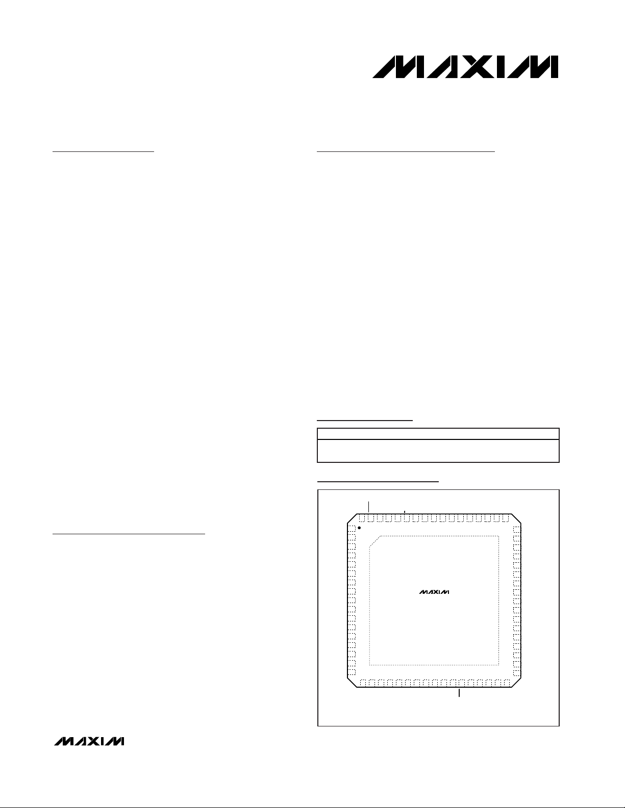
The MAX1127 is available in a small, 10mm x 10mm x
0.9mm, 68-pin QFN package with exposed paddle and
is specified for the extended industrial (-40°C to +85°C)
temperature range.
Applications
Ultrasound and Medical Imaging
Positron Emission Tomography (PET) Imaging
Multichannel Communication Systems
Instrumentation
Features
♦ Four ADC Channels with Serial LVDS/SLVS
Outputs
♦ Excellent Dynamic Performance
69.6dB SNR at fIN= 19.3MHz
92dBc SFDR at fIN= 19.3MHz
-87dB Channel Isolation
♦ Ultra-Low Power
135mW per Channel (Normal Operation)
1.2mW Total (Shutdown Mode)
♦ Accepts 20% to 80% Clock Duty Cycle
♦ Self-Aligning Data-Clock to Data-Output Interface
♦ Fully Differential Analog Inputs
♦ Wide ±1.4V
P-P
Differential Input Voltage Range
♦ Internal/External Reference Option
♦ Test Mode for Digital Signal Integrity
♦ LVDS Outputs Support Up to 30in FR-4 Backplane
Connections
♦ Small, 68-Pin QFN with Exposed Paddle
♦ Evaluation Kit Available (MAX1127EVKIT)
MAX1127
Quad, 12-Bit, 65Msps, 1.8V ADC with
Serial LVDS Outputs
________________________________________________________________ Maxim Integrated Products 1
Ordering Information
19-3144; Rev 1; 3/04
For pricing, delivery, and ordering information, please contact Maxim/Dallas Direct! at
1-888-629-4642, or visit Maxim’s website at www.maxim-ic.com.
PART TEMP RANGE PIN-PACKAGE
MAX1127EGK -40°C to +85°C
68 QFN 10mm x
x 10mm x 0.9mm
35 OUT3N
36 OUT3P
37 OV
DD
38 OUT2N
39 OUT2P
40 OV
DD
41 FRAMEN
42
FRAMEP
43
OV
DD
44
CLKOUTN
45 CLKOUTP
46 OV
DD
47 OUT1N
48 OUT1P
49 OV
DD
50 OUT0N
51 OUT0P
52
OV
DD
53
PD054PD155PD256PD357PDALL58AV
DD
59
AV
DD
60
AV
DD
61
AV
DD
62
AV
DD
6364
LVDSTEST
65
GND66REFIO
6768
GND
1GND
2IN0P
3IN0N
4GND
5IN1P
6IN1N
7GND
8AV
DD
9AV
DD
10AV
DD
11GND
12IN2P
13IN2N
14GND
15IN3P
16IN3N
17GND
18
AV
DD
19
I.C.
20
AV
DD
21
CV
DD
22
GND
23
CLK
24
GND
25
AV
DD
26
AV
DD
27
AV
DD
28DT29 30
PLL031PLL132PLL233PLL3
34
OV
DD
SLVS/LVDS
INTREF
T/B
MAX1127
QFN
10mm x 10mm x 0.9mm
EP
Pin Configuration
Page 2
MAX1127
Quad, 12-Bit, 65Msps, 1.8V ADC with
Serial LVDS Outputs
2 _______________________________________________________________________________________
ABSOLUTE MAXIMUM RATINGS
ELECTRICAL CHARACTERISTICS
(AV
DD
= 1.8V, OVDD= 1.8V, CVDD= 1.8V, GND = 0, external V
REFIO
= 1.24V, INTREF = AVDD, C
REFIO
to GND = 0.1µF,
f
CLK
= 65MHz (50% duty cycle), DT = 0, TA= T
MIN
to T
MAX
, unless otherwise noted. Typical values are at TA= +25°C.) (Note 1)
Stresses beyond those listed under “Absolute Maximum Ratings” may cause permanent damage to the device. These are stress ratings only, and functional
operation of the device at these or any other conditions beyond those indicated in the operational sections of the specifications is not implied. Exposure to
absolute maximum rating conditions for extended periods may affect device reliability.
AVDDto GND.........................................................-0.3V to +2.0V
CV
DD
to GND ........................................................-0.3V to +3.6V
OV
DD
to GND ........................................................-0.3V to +2.0V
IN_P, IN_N to GND...................................-0.3V to (AV
DD
+ 0.3V)
CLK to GND.............................................-0.3V to (CV
DD
+ 0.3V)
OUT_P, OUT_N, FRAME_,
CLKOUT_ to GND................................-0.3V to (OV
DD
+ 0.3V)
DT, SLVS/LVDS to GND...........................-0.3V to (AV
DD
+ 0.3V)
PLL0, PLL1, PLL2, PLL3 to GND .............-0.3V to (AV
DD
+ 0.3V)
PD0, PD1, PD2, PD3, PDALL to GND......-0.3V to (AV
DD
+ 0.3V)
T/B, LVDSTEST to GND ...........................-0.3V to (AV
DD
+ 0.3V)
REFIO, INTREF to GND............................-0.3V to (AV
DD
+ 0.3V)
I.C. to GND...............................................-0.3V to (AV
DD
+ 0.3V)
Continuous Power Dissipation (T
A
= +70°C)
68-Pin QFN 10mm x 10mm x 0.9mm
(derated 41.7mW/°C above +70°C)........................3333.3mW
Operating Temperature Range ...........................-40°C to +85°C
Maximum Junction Temperature .....................................+150°C
Storage Temperature Range .............................-65°C to +150°C
Lead Temperature Range (soldering, 10s)......................+300°C
PARAMETER
SYMBOL
CONDITIONS
MIN
TYP
MAX
UNITS
DC ACCURACY
Resolution N 12 Bits
Integral Nonlinearity INL (Note 2)
LSB
Differential Nonlinearity DNL (Note 2)
LSB
Offset Error
Gain Error
ANALOG INPUTS (IN_P, IN_N)
Input Differential Range V
ID
Differential input 1.4
Common-Mode Voltage Range V
CMO
(Note 3)
V
Differential Input Impedance R
IN
Switched capacitor load 2 kΩ
Differential Input Capacitance C
IN
pF
CONVERSION RATE
Maximum Conversion Rate f
SMAX
65
Minimum Conversion Rate f
SMIN
16
Data Latency 6.5
DYNAMIC CHARACTERISTICS (differential inputs, 4096-point FFT)
fIN = 5.3MHz at -0.5dBFS
fIN = 19.3MHz at -0.5dBFS, TA ≥ +25°C
Signal-to-Noise Ratio (Note 2) SNR
f
IN
= 30.3MHz at -0.5dBFS
dB
fIN = 5.3MHz at -0.5dBFS
fIN = 19.3MHz at -0.5dBFS, TA ≥ +25°C
Signal-to-Noise and Distortion
(First Four Harmonics) (Note 2)
SINAD
f
IN
= 30.3MHz at -0.5dBFS
dB
fIN = 5.3MHz at -0.5dBFS
fIN = 19.3MHz at -0.5dBFS, TA ≥ +25°C
Effective Number of Bits (Note 2)
ENOB
f
IN
= 30.3MHz at -0.5dBFS
Bits
Fixed external reference (Note 2) ±1
Fixed external reference (Note 2) ±1.5
±0.4
±0.25
% FS
% FS
66.6 69.6
66.5 69.5
0.75
12.5
69.7
69.4
69.6
69.3
11.4
11.4
11.3
V
P-P
MHz
MHz
Cycles
Page 3
MAX1127
Quad, 12-Bit, 65Msps, 1.8V ADC with
Serial LVDS Outputs
_______________________________________________________________________________________ 3
ELECTRICAL CHARACTERISTICS (continued)
(AV
DD
= 1.8V, OVDD= 1.8V, CVDD= 1.8V, GND = 0, external V
REFIO
= 1.24V, INTREF = AVDD, C
REFIO
to GND = 0.1µF,
f
CLK
= 65MHz (50% duty cycle), DT = 0, TA= T
MIN
to T
MAX
, unless otherwise noted. Typical values are at TA= +25°C.) (Note 1)
PARAMETER
CONDITIONS
UNITS
fIN = 5.3MHz at -0.5dBFS
fIN = 19.3MHz at -0.5dBFS, TA ≥ +25°C
92
Spurious-Free Dynamic Range
(Note 2)
SFDR
f
IN
= 30.3MHz at -0.5dBFS
dBc
fIN = 5.3MHz at -0.5dBFS -91
fIN = 19.3MHz at -0.5dBFS, TA ≥ +25°C -91
Total H ar m oni c D i stor ti on ( N ote 2)
THD
f
IN
= 30.3MHz at -0.5dBFS -88
dBc
Inter m od ul ati on D i stor ti on IMD
f
1
= 12.348685MHz at -6.5dBFS,
f
2
= 13.650845MHz at -6.5dBFS ( N ote 2)
dBc
Third-Order Intermodulation IM3 (Note 2)
dBc
Aperture Jitter t
AJ
(Note 2)
ps
RMS
Aperture Delay t
AD
(Note 2) 1 ns
Small-Signal Bandwidth SSBW Input at -20dBFS (Notes 2 and 4)
MHz
Full-Power Bandwidth LSBW Input at -0.5dBFS (Notes 2 and 4)
MHz
Output Noise INP = IN_N
LSB
RMS
Overdrive Recovery Time t
OR
RS = 25Ω, CS = 50pF 1
Clock
cycles
INTERNAL REFERENCE (INTREF = GND, bypass REFIO to GND with 0.1µF)
INTREF Internal Reference Mode
Enable Voltage
(Note 5) 0.1 V
INTREF Low-Leakage Current
µA
REFIO Output Voltage V
REFIO
V
Reference Temperature
Coefficient
ppm/°C
EXTERNAL REFERENCE (INTREF = AVDD)
INTREF External Reference Mode
Enable Voltage
(Note 5)
AV
DD
V
INTREF High-Leakage Current
µA
REFIO Input Voltage Range
V
REFIO Input Current I
REFIO
<1 µA
CLOCK INPUT (CLK)
Input High Voltage V
CLKH
0.8 x
V
Input Low Voltage V
CLKL
0.2 x
V
Clock Duty Cycle 50 %
Clock Duty-Cycle Tolerance
%
SYMBOL
TC
REFIO
MIN TYP MAX
77.5
1.18 1.24 1.30
93.3
88.9
91.2
95.7
<0.4
100
100
0.35
200
100
-77.5
0.1V
200
1.24
CV
DD
±30
CV
DD
Page 4
MAX1127
Quad, 12-Bit, 65Msps, 1.8V ADC with
Serial LVDS Outputs
4 _______________________________________________________________________________________
ELECTRICAL CHARACTERISTICS (continued)
(AV
DD
= 1.8V, OVDD= 1.8V, CVDD= 1.8V, GND = 0, external V
REFIO
= 1.24V, INTREF = AVDD, C
REFIO
to GND = 0.1µF,
f
CLK
= 65MHz (50% duty cycle), DT = 0, TA= T
MIN
to T
MAX
, unless otherwise noted. Typical values are at TA= +25°C.) (Note 1)
PARAMETER
CONDITIONS
Input at GND 5
Input Leakage DI
IN
Input at AV
DD
80
µA
Input Capacitance DC
IN
5pF
DIGITAL INPUTS (PLL_, LVDSTEST, DT, SLVS/LVDS, PD_, PDALL, T/B)
Input High Threshold V
IH
0.8 x
V
Input Low Threshold V
IL
0.2 x
V
Input at GND, except PLL2 and PLL3 5
Input at AVDD, except PLL2 and PLL3 80Input Leakage DI
IN
PLL2 and PLL3 only 200
µA
Input Capacitance DC
IN
5pF
LVDS OUTPUTS (OUT_P, OUT_N, SLVS/LVDS = 0)
Differential Output Voltage
R
TERM
= 100Ω
450 mV
Output Common-Mode Voltage V
OCM
R
TERM
= 100Ω
V
Rise Time (20% to 80%) t
R
R
TERM
= 100Ω, C
LOAD
= 5pF
ps
Fall Time (80% to 20%) t
F
R
TERM
= 100Ω, C
LOAD
= 5pF
ps
SLVS OUTPUTS (OUT_P, OUT_N, CLKOUTP, CLKOUTN, FRAMEP, FRAMEN), SLVS/LVDS = 1, DT = 1
Differential Output Voltage
R
TERM
= 100Ω
mV
Output Common-Mode Voltage V
OCM
R
TERM
= 100Ω
mV
Rise Time (20% to 80%) t
R
R
TERM
= 100Ω, C
LOAD
= 5pF
ps
Fall Time (80% to 20%) t
F
R
TERM
= 100Ω, C
LOAD
= 5pF
ps
POWER-DOWN
PD Fall to Output Enable
µs
PD Rise to Output Disable
10 ns
POWER REQUIREMENTS
AVDD Supply Voltage AV
DD
1.7 1.8 1.9 V
OVDD Supply Voltage OV
DD
1.7 1.8 1.9 V
CVDD Supply Voltage CV
DD
1.7 1.8 3.6 V
SYMBOL
MIN TYP MAX UNITS
AV
DD
AV
DD
V
OHDIFF
V
OHDIFF
t
ENABLE
t
DISABLE
250
1.125 1.375
150
150
240
220
120
120
132
Page 5
MAX1127
Quad, 12-Bit, 65Msps, 1.8V ADC with
Serial LVDS Outputs
_______________________________________________________________________________________ 5
ELECTRICAL CHARACTERISTICS (continued)
(AV
DD
= 1.8V, OVDD= 1.8V, CVDD= 1.8V, GND = 0, external V
REFIO
= 1.24V, INTREF = AVDD, C
REFIO
to GND = 0.1µF,
f
CLK
= 65MHz (50% duty cycle), DT = 0, TA= T
MIN
to T
MAX
, unless otherwise noted. Typical values are at TA= +25°C.) (Note 1)
PARAMETER
CONDITIONS
UNITS
PDALL = 0, all channels
active
295
PDALL = 0, all channels
active, DT = 1
82
23
mA
AVDD Supply Current I
AVDD
f
IN
=
-0.5dBFS
PDALL = 1, global power
down, PD[3:0] =1111, no
clock input
µA
PDALL = 0, all channels
active
56 65
PDALL = 0, all channels
active, DT = 1
72
42
37
mA
OVDD Supply Current I
OVDD
f
IN
=
-0.5dBFS
PDALL = 1, global powerdown, PD[3:0] =1111, no
clock input
µA
CVDD Supply Current I
CVDD
CVDD is used only to bias ESD-protection
diodes on CLK input, Figure 2
0mA
Power Dissipation P
DISSfIN
= 19.3MHz at -0.5dBFS
648 mW
TIMING CHARACTERISTICS (Note 6)
Data Valid to CLKOUT Rise/Fall t
OD
f
CLK
= 65MHz, Figure 5 (Notes 6 and 7)
24)
t
SAMPLE
/
24
(t
SAMPLE
/
24)
ns
CLKOUT Output Width High t
CH
Figure 5
12
ns
CLKOUT Output Width Low t
CL
Figure 5
12
ns
FRAME Rise to CLKOUT Rise t
CF
Figure 4 (Note 7)
24)
t
SAMPLE
/
24
( t
SAMPLE
/
24)
ns
Sample CLK Rise to Frame Rise t
SF
Figure 4 (Notes 7 and 8)
2)
(t
SAMPLE
/
2)
(t
SAMPLE
/
2)
ns
SYMBOL
19.3MHz at
19.3MHz at
PDALL = 0, 1 channel active
PDALL = 0, PD[3:0] = 1111
PDALL = 0, 1 channel active
PDALL = 0, PD[3:0] = 1111
MIN TYP MAX
257
257
300
375
(t
SAMPLE
- 0.15
(t
SAMPLE
- 0.15
(t
SAMPLE
+0.9
563
/
t
S AMP LE
t
S AMP LE
/
/
+1.3
+ 0.15
/
/
+ 0.15
+1.7
Page 6
MAX1127
Quad, 12-Bit, 65Msps, 1.8V ADC with
Serial LVDS Outputs
6 _______________________________________________________________________________________
Note 1: Specifications at TA≥ +25°C are guaranteed by production testing. Specifications at TA< +25°C are guaranteed by design
and characterization and not subject to production testing.
Note 2: See definition in the
Parameter Definitions section.
Note 3: The MAX1127 internally sets the common-mode voltage to 0.6V (typ) (see Figure 1). The common-mode voltage can be
overdriven to between 0.55V and 0.85V.
Note 4: Limited by MAX1127EVKIT input circuitry.
Note 5: Connect INTREF to GND directly to enable internal reference mode. Connect INTREF to AV
DD
directly to disable the internal
bandgap reference and enable external reference mode.
Note 6: Data valid to CLKOUT rise/fall timing is measured from 50% of data output level to 50% of clock output level.
Note 7: Guaranteed by design and characterization. Not subject to production testing.
Note 8: Sample CLK rise to FRAME rise timing is measured from 50% of sample clock input level to 50% of FRAME output level.
ELECTRICAL CHARACTERISTICS (continued)
(AV
DD
= 1.8V, OVDD= 1.8V, CVDD= 1.8V, GND = 0, external V
REFIO
= 1.24V, INTREF = AVDD, C
REFIO
to GND = 0.1µF,
f
CLK
= 65MHz (50% duty cycle), DT = 0, TA= T
MIN
to T
MAX
, unless otherwise noted. Typical values are at TA= +25°C.) (Note 1)
PARAMETER
SYMBOL
CONDITIONS
MIN
TYP
MAX
UNITS
CHANNEL-TO-CHANNEL MATCHING
Crosstalk (Note 2) -87 dB
Gain Matching fIN = 30.3MHz (Note 2)
dB
Phase Matching fIN = 30.3.MHz (Note 2) ±1
Degrees
±0.1
Page 7
MAX1127
Quad, 12-Bit, 65Msps, 1.8V ADC with
Serial LVDS Outputs
_______________________________________________________________________________________ 7
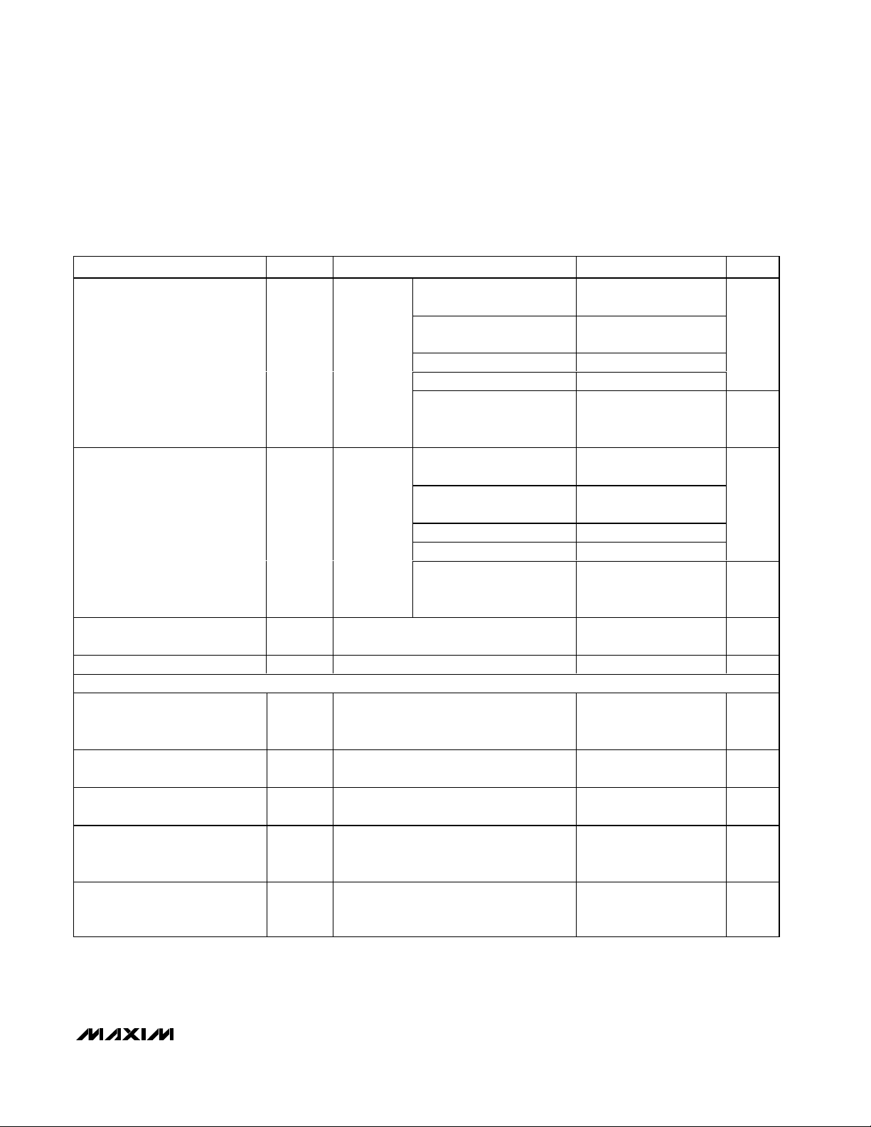
FFT PLOT
(32,768-POINT DATA RECORD)
MAX1127 toc01
FREQUENCY (MHz)
AMPLITUDE (dBFS)
284 8 12 2016 24
-110
-90
-100
-80
-70
-50
-30
-10
-60
-40
-20
0
-120
032
f
CLK
= 65.04448MHz
f
IN
= 5.301935MHz
A
IN
= -0.5dBFS
SNR = 69.5dB
SINAD = 69.47dB
THD = -90.94dBc
SFDR = 93.27dBc
HD2
HD3
FFT PLOT
(32,768-POINT DATA RECORD)
MAX1127toc02
FREQUENCY (MHz)
AMPLITUDE (dBFS)
284 8 12 2016 24
-110
HD3
-90
-100
-80
-70
-50
-30
-10
-60
-40
-20
0
-120
032
f
CLK
= 65.04448MHz
f
IN
= 30.30301MHz
A
IN
= -0.5dBFS
SNR = 69.45dB
SINAD = 69.4dB
THD = -89.3dBc
SFDR = 89.7dBc
HD2
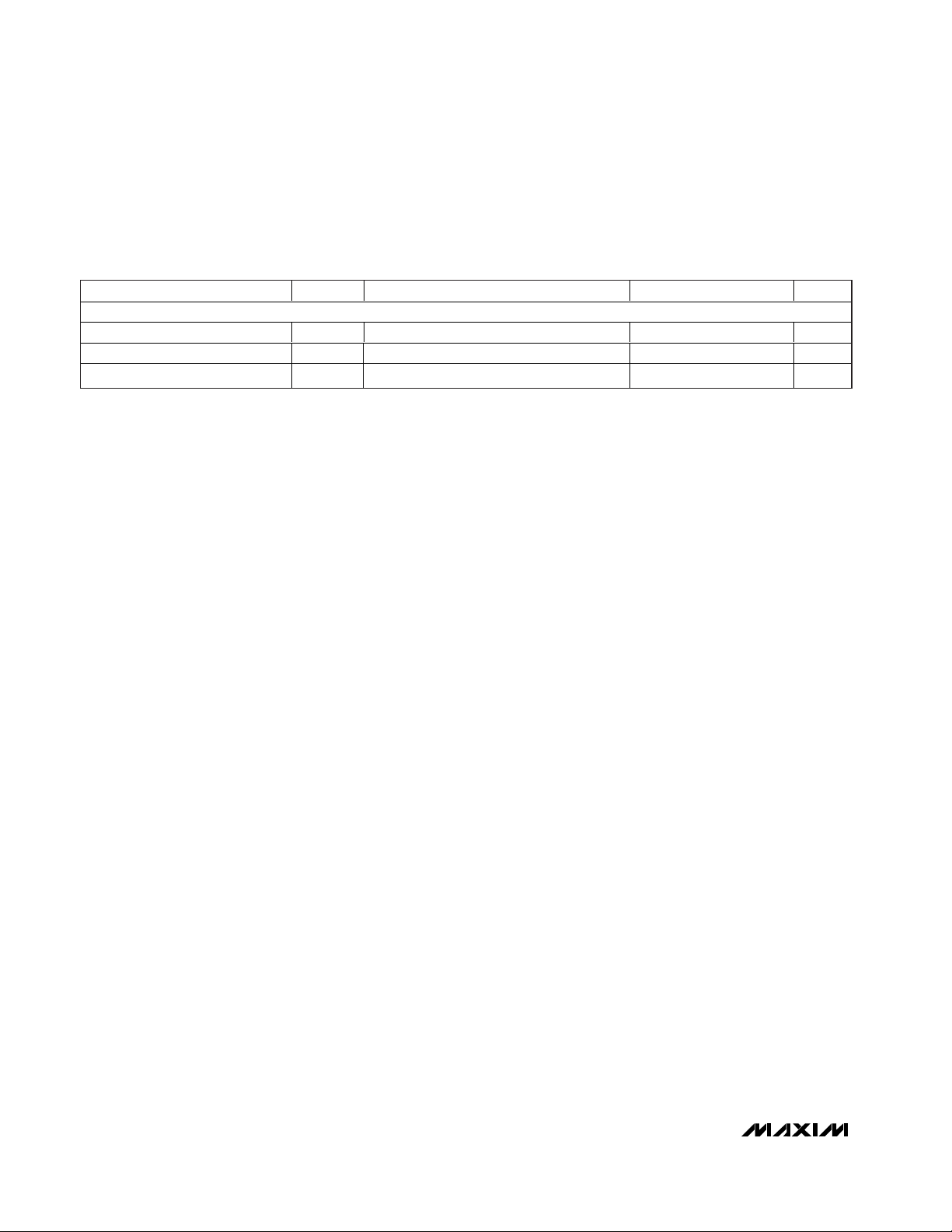
CROSSTALK
(4096-POINT DATA RECORD)
MAX1127 toc03
FREQUENCY (MHz)
AMPLITUDE (dBFS)
284 8 12 2016 24
-90
-100
-80
-70
-50
-30
-10
-60
-40
-20
0
-110
032
MEASURED ON CHANNEL 1,
WITH INTERFERING SIGNAL
ON CHANNEL 0.
f
IN(IN1)
= 5.3489349MHz
f
IN(IN0)
= 30.2683055MHz
CROSSTALK
(4096-POINT DATA RECORD)
MAX1127 toc04
FREQUENCY (MHz)
AMPLITUDE (dBFS)
284 8 12 2016 24
-90
-100
-80
-70
-50
-30
-10
-60
-40
-20
0
-110
032
MEASURED ON CHANNEL 1,
WITH INTERFERING SIGNAL
ON CHANNEL 2.
f
IN(IN1)
= 5.3489349MHz
f
IN(IN2)
= 30.2683055MHz
CROSSTALK
(4096-POINT DATA RECORD)
MAX1127 toc05
FREQUENCY (MHz)
AMPLITUDE (dBFS)
284 8 12 2016 24
-90
-100
-80
-70
-50
-30
-10
-60
-40
-20
0
-110
032
MEASURED ON CHANNEL 1,
WITH INTERFERING SIGNAL
ON CHANNEL 3.
f
IN(IN1)
= 5.3489349MHz
f
IN(IN3)
= 30.2683055MHz
TWO-TONE INTERMODULATION DISTORTION
(32,768-POINT DATA RECORD)
MAX1127 toc06
FREQUENCY (MHz)
AMPLITUDE (dBFS)
284 8 12 2016 24
-110
-90
-100
-80
-70
-50
-30
-10
-60
-40
-20
0
-120
032
f
IN(IN1)
= 12.348685MHz
f
IN(IN2)
= 13.650845MHz
A
IN1
= -6.5dBFS
A
IN2
= -6.5dBFS
IMD = 91.2dBc
IM3 = 95.7dBc
1
-7
1 100 1000
GAIN BANDWIDTH PLOT
-5
-6
-4
-3
-2
-1
0
MAX1127 toc07
ANALOG INPUT FREQUENCY (MHz)
GAIN (dB)
10
SMALL-SIGNAL
BANDWIDTH
-20dBFS
FULL-POWER
BANDWIDTH
-0.5dBFS
LIMITED BY
MAX1127EVKIT
INPUT CIRCUITRY
Typical Operating Characteristics
(AVDD= 1.8V, OVDD= 1.8V, CVDD= 1.8V, GND = 0, external V
REFIO
= 1.24V, INTREF = AVDD, differential input at -0.5dBFS,
f
CLK
= 65MHz (50% duty cycle), DT = low, C
LOAD
= 10pF, TA= +25°C, unless otherwise noted.)
Page 8
MAX1127
Quad, 12-Bit, 65Msps, 1.8V ADC with
Serial LVDS Outputs
8 _______________________________________________________________________________________
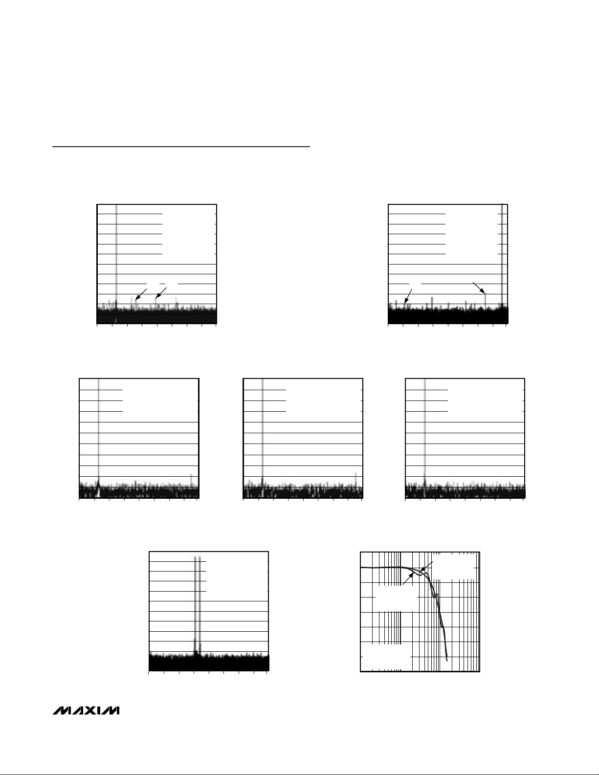
SIGNAL-TO-NOISE RATIO
vs. ANALOG INPUT FREQUENCY
fIN (MHz)
SNR (dB)
1008020 40 60
63
64
65
67
69
66
68
70
71
MAX1127 toc08
72
62
0 120
SIGNAL-TO-NOISE + DISTORTION
vs. ANALOG INPUT FREQUENCY
fIN (MHz)
SINAD (dB)
1008020 40 60
63
64
65
67
69
66
68
70
71
MAX1127 toc09
72
62
0 120
TOTAL HARMONIC DISTORTION
vs. ANALOG INPUT FREQUENCY
fIN (MHz)
THD (dBc)
1008020 40 60
-95
-90
-85
-75
-70
-80
-65
-60
MAX1127 toc10
-55
-100
0 120
SPURIOUS-FREE DYNAMIC RANGE
vs. ANALOG INPUT FREQUENCY
fIN (MHz)
SFDR (dBc)
1008020 40 60
60
65
70
80
85
75
90
95
MAX1127 toc11
100
55
0 120
Typical Operating Characteristics (continued)
(AVDD= 1.8V, OVDD= 1.8V, CVDD= 1.8V, GND = 0, external V
REFIO
= 1.24V, INTREF = AVDD, differential input at -0.5dBFS,
f
CLK
= 65MHz (50% duty cycle), DT = low, C
LOAD
= 10pF, TA= +25°C, unless otherwise noted.)
Page 9

MAX1127
Quad, 12-Bit, 65Msps, 1.8V ADC with
Serial LVDS Outputs
_______________________________________________________________________________________ 9
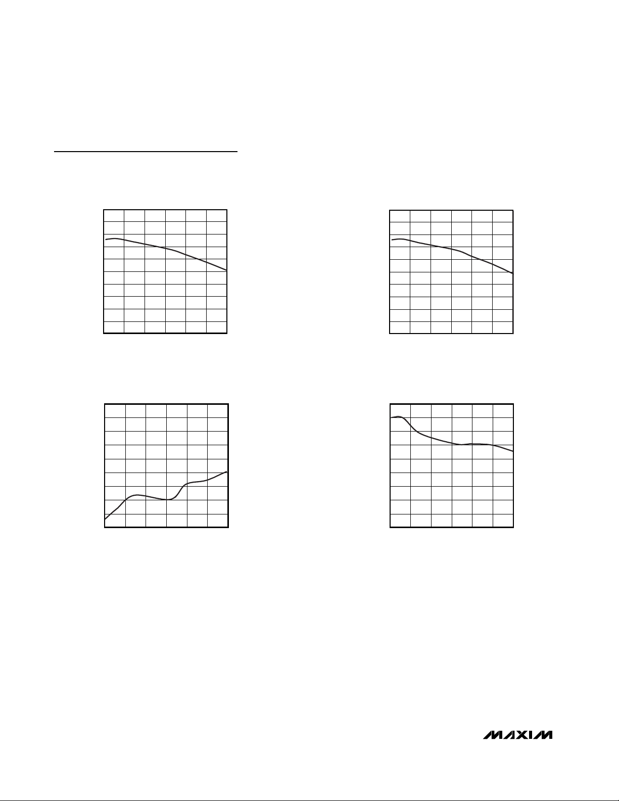
SIGNAL-TO-NOISE RATIO
vs. ANALOG INPUT POWER
ANALOG INPUT POWER (dBFS)
SNR (dB)
-5-10-25 -20 -15
37
42
52
57
47
62
67
72
32
-30 0
MAX1127 toc12
fIN = 5.301935MHz
SIGNAL TO NOISE + DISTORTION
vs. ANALOG INPUT POWER
ANALOG INPUT POWER (dBFS)
SINAD (dB)
-5-10-25 -20 -15
37
42
52
57
47
62
MAX1127 toc13
67
72
32
-30 0
fIN = 5.301935MHz
TOTAL HARMONIC DISTORTION
vs. ANALOG INPUT POWER
ANALOG INPUT POWER (dBFS)
THD (dBc)
-5-10-25 -20 -15
-90
-95
-85
-75
-70
-80
-65
-60
-55
-100
-30 0
MAX1127 toc14
fIN = 5.301935MHz
SPURIOUS-FREE DYNAMIC RANGE
vs. ANALOG INPUT POWER
ANALOG INPUT POWER (dBFS)
SFDR (dBc)
-5-10-25 -20 -15
65
60
70
80
85
75
90
95
100
55
-30 0
MAX1127 toc15
fIN = 5.301935MHz
Typical Operating Characteristics (continued)
(AVDD= 1.8V, OVDD= 1.8V, CVDD= 1.8V, GND = 0, external V
REFIO
= 1.24V, INTREF = AVDD, differential input at -0.5dBFS,
f
CLK
= 65MHz (50% duty cycle), DT = low, C
LOAD
= 10pF, TA= +25°C, unless otherwise noted.)
Page 10

MAX1127
Quad, 12-Bit, 65Msps, 1.8V ADC with
Serial LVDS Outputs
10 ______________________________________________________________________________________
SIGNAL-TO-NOISE RATIO
vs. SAMPLING RATE
f
CLK
(MHz)
SNR (dB)
5525 35 45 6030 40 50
65
64
63
66
68
69
67
70
71
72
62
20 65
MAX1127 toc16
fIN = 5.301935MHz
SIGNAL-TO-NOISE + DISTORTION
vs. SAMPLING RATE
f
CLK
(MHz)
SINAD (dB)
5525 35 45 6030 40 50
65
64
63
66
68
69
67
70
71
72
62
20 65
MAX1127 toc17
fIN = 5.301935MHz
TOTAL HARMONIC DISTORTION
vs. SAMPLING RATE
f
CLK
(MHz)
THD (dBc)
5525 35 45 6030 40 50
-95
-90
-100
-85
-80
-75
-105
20 65
MAX1127 toc18
fIN = 5.301935MHz
SPURIOUS-FREE DYNAMIC RANGE
vs. SAMPLING RATE
f
CLK
(MHz)
SFDR (dBc)
5525 35 45 6030 40 50
MAX1127 toc19
85
90
80
95
100
105
75
20 65
fIN = 5.301935MHz
Typical Operating Characteristics (continued)
(AVDD= 1.8V, OVDD= 1.8V, CVDD= 1.8V, GND = 0, external V
REFIO
= 1.24V, INTREF = AVDD, differential input at -0.5dBFS,
f
CLK
= 65MHz (50% duty cycle), DT = low, C
LOAD
= 10pF, TA= +25°C, unless otherwise noted.)
Page 11

MAX1127
Quad, 12-Bit, 65Msps, 1.8V ADC with
Serial LVDS Outputs
______________________________________________________________________________________ 11
SIGNAL-TO-NOISE RATIO
vs. CLOCK DUTY CYCLE
CLOCK DUTY CYCLE (%)
SNR (dB)
6040 50
65
67
63
69
71
64
66
68
70
72
62
30 70
MAX1127 toc20
fIN = 5.301935MHz
SIGNAL-TO-NOISE + DISTORTION
vs. CLOCK DUTY CYCLE
CLOCK DUTY CYCLE (%)
SINAD (dB)
6040 50
65
67
63
69
71
64
66
68
70
72
62
30 70
MAX1127 toc21
fIN = 5.301935MHz
TOTAL HARMONIC DISTORTION
vs. CLOCK DUTY CYCLE
CLOCK DUTY CYCLE (%)
THD (dBc)
40 6050
MAX1127 toc22
-95
-90
-100
-85
-80
-75
-105
30 70
fIN = 5.301935MHz
SPURIOUS-FREE DYNAMIC RANGE
vs. CLOCK DUTY CYCLE
CLOCK DUTY CYCLE (%)
SFDR (dBc)
40 6050
80
85
75
90
95
100
70
30 70
MAX1127 toc23
fIN = 5.301935MHz
Typical Operating Characteristics (continued)
(AVDD= 1.8V, OVDD= 1.8V, CVDD= 1.8V, GND = 0, external V
REFIO
= 1.24V, INTREF = AVDD, differential input at -0.5dBFS,
f
CLK
= 65MHz (50% duty cycle), DT = low, C
LOAD
= 10pF, TA= +25°C, unless otherwise noted.)
Page 12

MAX1127
Quad, 12-Bit, 65Msps, 1.8V ADC with
Serial LVDS Outputs
12 ______________________________________________________________________________________
Typical Operating Characteristics (continued)
(AVDD= 1.8V, OVDD= 1.8V, CVDD= 1.8V, GND = 0, external V
REFIO
= 1.24V, INTREF = AVDD, differential input at -0.5dBFS,
f
CLK
= 65MHz (50% duty cycle), DT = low, C
LOAD
= 10pF, TA= +25°C, unless otherwise noted.)
SIGNAL-TO-NOISE RATIO
vs. TEMPERATURE
TEMPERATURE (°C)
SNR (dB)
-15 10 6035
66
68
64
70
72
62
-40 85
MAX1127 toc24
f
CLK
= 65.04065041MHz
f
IN
= 19.29703379MHz
4096-POINT DATA RECORD
SIGNAL-TO-NOISE + DISTORTION
vs. TEMPERATURE
TEMPERATURE (°C)
SINAD (dB)
-15 10 6035
66
68
64
70
72
62
-40 85
MAX1127 toc25
f
CLK
= 65.04065041MHz
f
IN
= 19.29703379MHz
4096-POINT DATA RECORD
TOTAL HARMONIC DISTORTION
vs. TEMPERATURE
TEMPERATURE (°C)
THD (dBc)
-15 10 6035
-95
-90
-100
-85
-80
-75
-105
-40 85
MAX1127 toc26
f
CLK
= 65.04065041MHz
f
IN
= 19.29703379MHz
4096-POINT DATA RECORD
SPURIOUS-FREE DYNAMIC RANGE
vs. TEMPERATURE
TEMPERATURE (°C)
SFDR (dBc)
-15 10 6035
85
90
80
75
95
100
70
-40 85
MAX1127 toc27
f
CLK
= 65.04065041MHz
f
IN
= 19.29703379MHz
4096-POINT DATA RECORD
Page 13

MAX1127
Quad, 12-Bit, 65Msps, 1.8V ADC with
Serial LVDS Outputs
______________________________________________________________________________________ 13
ANALOG SUPPLY CURRENT
vs. SAMPLING RATE
f
CLK
(MHz)
I
AVDD
(mA)
30 504025 45 605535
MAX1127 toc28
240
250
230
260
270
220
20 65
DIGITAL SUPPLY CURRENT
vs. SAMPLING RATE
f
CLK
(MHz)
I
OVDD
(mA)
30 504025 45 605535
MAX1127 toc29
20
40
10
60
30
50
70
0
20 65
OFFSET ERROR
vs. TEMPERATURE
TEMPERATURE (°C)
OFFSET ERROR (%FS)
-15 10 6035
0.03
0.04
0.02
0.05
0.06
0.01
-40 85
MAX1127 toc30
GAIN ERROR
vs. TEMPERATURE
TEMPERATURE (°C)
GAIN ERROR (%FS)
-15 10 6035
0.2
0.6
-.0.2
-0.6
0
0.4
-0.4
-0.8
0.8
1.0
-1.0
-40 85
MAX1127 toc31
DIFFERENTIAL NONLINEARITY
vs. DIGITAL OUTPUT CODE
MAX1127 toc33
DIGITAL OUTPUT CODE
DNL (LSB)
1024 30722048512 2560 35841536
-0.3
0
-0.4
0.4
-0.2
0.2
-0.1
0.3
0.1
0.5
-0.5
0 4096
Typical Operating Characteristics (continued)
(AVDD= 1.8V, OVDD= 1.8V, CVDD= 1.8V, GND = 0, external V
REFIO
= 1.24V, INTREF = AVDD, differential input at -0.5dBFS,
f
CLK
= 65MHz (50% duty cycle), DT = low, C
LOAD
= 10pF, TA= +25°C, unless otherwise noted.)
0.5
0.4
0.3
0.2
0.1
0
INL (LSB)
-0.1
-0.2
-0.3
-0.4
-0.5
0 4096
INTEGRAL NONLINEARITY
vs. DIGITAL OUTPUT CODE
1024 30722048512 2560 35841536
DIGITAL OUTPUT CODE
MAX1127 toc32
Page 14

MAX1127
Quad, 12-Bit, 65Msps, 1.8V ADC with
Serial LVDS Outputs
14 ______________________________________________________________________________________
Typical Operating Characteristics (continued)
(AVDD= 1.8V, OVDD= 1.8V, CVDD= 1.8V, GND = 0, external V
REFIO
= 1.24V, INTREF = AVDD, differential input at -0.5dBFS,
f
CLK
= 65MHz (50% duty cycle), DT = low, C
LOAD
= 10pF, TA= +25°C, unless otherwise noted.)
INTERNAL REFERENCE VOLTAGE
vs. SUPPLY VOLTAGE
SUPPLY VOLTAGE (V)
V
REFIO
(V)
2.01.91.8
1.236
1.237
1.238
1.239
1.235
1.7 2.1
MAX1127 toc34
AVDD = OV
DD
INTERNAL REFERENCE VOLTAGE
vs. TEMPERATURE
TEMPERATURE (°C)
V
REFIO
(V)
603510-15
1.23
1.24
1.25
1.26
1.22
-40 85
MAX1127 toc35
AVDD = OV
DD
INTERNAL REFERENCE VOLTAGE
vs. REFERENCE LOAD CURRENT
I
REFIO
(µA)
V
REFIO
(V)
300200-300 -200 -100 0 100
1.05
1.10
1.15
1.20
1.25
1.30
1.35
1.40
1.00
-400 400
MAX1127 toc36
NEGATIVE CURRENT
FLOWS INTO REFIO
PIN NAME FUNCTION
1, 4, 7, 11,
14, 17, 22,
24, 65, 68
GND Ground. Connect all GND pins to the same potential.
2 IN0P Channel 0 Positive Analog Input
3 IN0N Channel 0 Negative Analog Input
5 IN1P Channel 1 Positive Analog Input
6 IN1N Channel 1 Negative Analog Input
8, 9, 10, 18,
20, 25, 26,
27, 58–62
AV
DD
Analog Power Input. Connect AVDD to a 1.7V to 1.9V power supply. Bypass each AVDD to GND with
a 0.1µF capacitor as close to the device as possible. Bypass the AV
DD
power plane to the GND
ground plane with a bulk ≥2.2µF capacitor as close to the device as possible. Connect all AV
DD
pins
to the same potential.
12 IN2P Channel 2 Positive Analog Input
13 IN2N Channel 2 Negative Analog Input
15 IN3P Channel 3 Positive Analog Input
16 IN3N Channel 3 Negative Analog Input
19 I.C. Internally Connected. Do not connect.
21 CV
DD
Clock Power Input. Connect CVDD to a 1.7V to 3.6V supply. Bypass CVDD to GND with a 0.1µF
capacitor in parallel with a ≥2.2µF capacitor. Install the bypass capacitors as close to the device as
possible.
23 CLK Single-Ended CMOS Clock Input
28 DT
Double Termination Select Input. Drive DT high to select the internal 100Ω termination between the
differential output pairs. Drive DT low to select no internal output termination.
Pin Description
Page 15

MAX1127
Quad, 12-Bit, 65Msps, 1.8V ADC with
Serial LVDS Outputs
______________________________________________________________________________________ 15
PIN NAME FUNCTION
29
Differential Output Signal Format Select Input. Drive SLVS/LVDS high to select SLVS outputs. Drive
SLVS/LVDS low to select LVDS outputs.
30 PLL0
PLL Control Input 0. PLL0 is reserved for factory testing only and must always be connected to GND.
31 PLL1
PLL Control Input 1. PLL1 is reserved for factory testing only and must always be connected to GND.
32 PLL2 PLL Control Input 2. See Table 1 for details.
33 PLL3 PLL Control Input 3. See Table 1 for details.
34, 37, 40,
43, 46, 49,
52
OV
DD
Output-Driver Power Input. Connect OVDD to a 1.7V to 1.9V power supply. Bypass each OVDD to
GND with a 0.1µF capacitor as close to the device as possible. Bypass the OV
DD
power plane to the
GND ground plane with a bulk ≥2.2µF capacitor as close to the device as possible. Connect all OV
DD
pins to the same potential.
35 OUT3N Channel 3 Negative LVDS/SLVS Output
36 OUT3P Channel 3 Positive LVDS/SLVS Output
38 OUT2N Channel 2 Negative LVDS/SLVS Output
39 OUT2P Channel 2 Positive LVDS/SLVS Output
41 FRAMEN
Negative Frame Alignment LVDS/SLVS Output. A rising edge on the differential FRAME output aligns
to a valid D0 in the output data stream.
42 FRAMEP
Positive Frame Alignment LVDS/SLVS Output. A rising edge on the differential FRAME output aligns to
a valid D0 in the output data stream.
44
Negative LVDS/SLVS Serial Clock Output
45
Positive LVDS/SLVS Serial Clock Output
47 OUT1N Channel 1 Negative LVDS/SLVS Output
48 OUT1P Channel 1 Positive LVDS/SLVS Output
50 OUT0N Channel 0 Negative LVDS/SLVS Output
51 OUT0P Channel 0 Positive LVDS/SLVS Output
53 PD0
Channel 0 Power-Down Input. Drive PD0 high to power-down channel 0. Drive PD0 low for normal
operation.
54 PD1
Channel 1 Power-Down Input. Drive PD1 high to power-down channel 1. Drive PD1 low for normal
operation.
55 PD2
Channel 2 Power-Down Input. Drive PD2 high to power-down channel 2. Drive PD2 low for normal
operation.
56 PD3
Channel 3 Power-Down Input. Drive PD3 high to power-down channel 3. Drive PD3 low for normal
operation.
57 PDALL
Global Power-Down Input. Drive PDALL high to power-down all channels and reference. Drive PDALL
low for normal operation.
63 T/B
Output Format Select Input. Drive T/B high to select binary output format. Drive T/B low to select two’s
complement output format.
Pin Description (continued)
SLVS/LVDS
CLKOUTN
CLKOUTP
Page 16

MAX1127
Quad, 12-Bit, 65Msps, 1.8V ADC with
Serial LVDS Outputs
16 ______________________________________________________________________________________
LVDS/SLVS
OUTPUT
DRIVERS
REFERENCE
SYSTEM
PLL
6x
CLOCK
CIRCUITRY
POWER CONTROL
REFIO
INTREF
IN0P
IN0N
IN1P
IN1N
IN2P
IN2N
IN3P
IN3N
CLK
PDALL PD0 PD1 PD2 PD3
OUT0P
OUT0N
OUT1P
OUT1N
OUT2P
OUT2N
OUT3P
OUT3N
CLKOUTP
CLKOUTN
OV
DD
AV
DD
GND
CV
DD PLL3PLL0 PLL1 PLL2
T/B
LVDSTEST
FRAMEP
FRAMEN
DT
OUTPUT
CONTROL
MAX1127
T/H
12-BIT
PIPELINE
ADC
12:1
SERIALIZER
T/H
12-BIT
PIPELINE
ADC
12:1
SERIALIZER
T/H
12-BIT
PIPELINE
ADC
12:1
SERIALIZER
T/H
12-BIT
PIPELINE
ADC
12:1
SERIALIZER
SLVS/LVDS
Functional Diagram
PIN NAME FUNCTION
64
LVDS Test Pattern Enable Input. Drive LVDSTEST high to enable the output test pattern
(000010111101 MSB→LSB). As with the analog conversion results, the test pattern data is output
LSB first. Drive LVDSTEST low for normal operation.
66 REFIO
Reference Input/Output. For internal reference operation (INTREF = GND), the reference output
voltage is 1.24V. For external reference operation (INTREF = AVDD), apply a stable reference voltage
at REFIO. Bypass to GND with a 0.1µF capacitor.
67 INTREF
Internal/External Reference Mode Select Input. For internal reference mode, connect INTREF directly
to GND. For external reference mode, connect INTREF directly to AV
DD
.
—EP
Exposed Paddle. EP is internally connected to GND. Externally connect EP to GND to achieve
specified performance.
Pin Description (continued)
LVDSTEST
Page 17

MAX1127
Quad, 12-Bit, 65Msps, 1.8V ADC with
Serial LVDS Outputs
______________________________________________________________________________________ 17
Detailed Description
The MAX1127 ADC features fully differential inputs, a
pipelined architecture, and digital error correction for
high-speed signal conversion. The ADC pipeline architecture moves the samples taken at the inputs through
the pipeline stages every half clock cycle. The converted digital results are serialized and sent through the
LVDS/SLVS output drivers. The total latency from input
to output is 6.5 input clock cycles.
The MAX1127 offers four separate fully differential
channels with synchronized inputs and outputs.
Configure the outputs for binary or two’s complement
with the T/B digital input. Power-down each channel
individually or globally to minimize power consumption.
Input Circuit
Figure 1 displays a simplified functional diagram of the
input T/H circuits. In track mode, switches S1, S2a, S2b,
S4a, S4b, S5a, and S5b are closed. The fully differential
circuits sample the input signals onto the two capacitors
(C2a and C2b) through switches S4a and S4b. S2a and
S2b set the common mode for the operational transcon-
ductance amplifier (OTA), and open simultaneously with
S1, sampling the input waveform. Switches S4a, S4b,
S5a, and S5b are then opened before switches S3a and
S3b connect capacitors C1a and C1b to the output of
the amplifier and switch S4c is closed. The resulting differential voltages are held on capacitors C2a and C2b.
The amplifiers charge capacitors C1a and C1b to the
same values originally held on C2a and C2b. These values are then presented to the first-stage quantizers and
isolate the pipelines from the fast-changing inputs.
Analog inputs IN_P to IN_N are driven differentially. For
differential inputs, balance the input impedance of IN_P
and IN_N for optimum performance.
The MAX1127 analog inputs are self-biased at a common-mode voltage of 0.6V (typ) and allow a differential
input voltage swing of 1.4V
P-P
. The common-mode voltage can be overdriven to between 0.55V to 0.85V.
Drive the analog inputs of the MAX1127 in AC-coupled
configuration to achieve best dynamic performance.
See the Using Transformer Coupling section for a
detailed discussion of this configuration.
MAX1127
IN_P
IN_N
OTA
AV
DD
GND
C2a
S4b
S4c S1
C2b
S4a
C1a
S2a
S5a
S3a
S3b
S5b
C1b
S2b
INTERNAL
BIAS*
OUT
INTERNALLY
GENERATED
COMMON-MODE
LEVEL*
SWITCHES SHOWN IN TRACK MODE
INTERNALLY
GENERATED
COMMON-MODE
LEVEL*
INTERNAL
COMMON-MODE
BIAS*
INTERNAL
COMMON-MODE
BIAS*
*NOT EXTERNALLY ACCESSIBLE
INTERNAL
BIAS*
OUT
Figure 1. Internal Input Circuitry
Page 18

MAX1127
Quad, 12-Bit, 65Msps, 1.8V ADC with
Serial LVDS Outputs
18 ______________________________________________________________________________________
Reference Configurations
(REFIO and
INTREF
)
The MAX1127 provides an internal 1.24V bandgap reference or can be driven with an external reference voltage. The MAX1127 full-scale analog differential input
range is ±FSR. Full-scale range (FSR) is given by the
following equation:
where V
REFIO
is the voltage at REFIO, generated inter-
nally or externally. For a V
REFIO
= 1.24V, the full-scale
input range is ±700mV (1.4V
P-P
).
Internal Reference Mode
Connect INTREF to GND to use the internal bandgap
reference directly. The internal bandgap reference generates REFIO to be 1.24V with a 100ppm/°C temperature coefficient in internal reference mode. Connect an
external ≥0.1µF bypass capacitor from REFIO to GND
for stability. REFIO sources up to 200µA and sinks up
to 200µA for external circuits, and REFIO has a load
regulation of 83mV/mA. The global power-down input
(PDALL) enables and disables the reference circuit.
REFIO has >1MΩ resistance to GND when the
MAX1127 is in power-down mode. The internal reference circuit requires 132µs to power-up and settle
when power is applied to the MAX1127 or when PDALL
transitions from high to low.
External Reference Mode
The external reference mode allows for more control
over the MAX1127 reference voltage and allows multiple converters to use a common reference. Connect
INTREF to AVDDto disable the internal reference and
enter external reference mode. Apply a stable 1.24V
source at REFIO. Bypass REFIO to GND with a 0.1µF
capacitor. The REFIO input impedance is >1MΩ.
Clock Input (CLK)
The MAX1127 accepts a CMOS-compatible clock signal with a wide 20% to 80% input-clock duty cycle.
Drive CLK with an external single-ended clock signal.
Figure 2 shows the simplified clock input diagram.
Low clock jitter is required for the specified SNR performance of the MAX1127. Analog input sampling occurs
on the rising edge of CLK, requiring this edge to provide the lowest possible jitter. Jitter limits the maximum
SNR performance of any ADC according to the following relationship:
where fINrepresents the analog input frequency and t
J
is the total system clock jitter. Clock jitter is especially
critical for undersampling applications. For example,
assuming that clock jitter is the only noise source, to
obtain the specified 69.4dB of SNR with an input frequency of 30.3MHz, the system must have less than
1.8ps of clock jitter. In actuality, there are other noise
sources, such as thermal noise and quantization noise,
that contribute to the system noise requiring the clock
jitter to be less than 0.5ps to obtain the specified
69.4dB of SNR at 30.3MHz.
The MAX1127 features a PLL that generates an output
clock signal with six times the frequency of the input
clock. The output clock signal is used to clock data out
of the MAX1127 (see the System Timing Requirements
section). Set the PLL2 and PLL3 bits according to the
input clock range provided in Table 1. PLL0 and PLL1
are reserved for factory testing and must always be
connected to GND.
SNR
ft
IN J
=×
×× ×
20
1
2
log
π
FSR mV
V
V
REFIO
=×700
124.
MAX1127
DUTY-CYCLE
EQUALIZER
AV
DD
CV
DD
CLK
GND
Figure 2. Clock Input Circuitry
CLOCK INPUT RANGE
(MHz)
PLL2 PLL3
MIN MAX
0048.750 65.000
0132.500 48.750
1024.375 32.500
1116.000 24.375
Table 1. PLL2 and PLL3 Configuration
*PLL0 and PLL11 are reserved for factory testing and must
always be connected to GND.
Page 19

MAX1127
Quad, 12-Bit, 65Msps, 1.8V ADC with
Serial LVDS Outputs
______________________________________________________________________________________ 19
System Timing Requirements
Figure 3 shows the relationship between the analog
inputs, input clock, frame alignment output, serial clock
output, and serial data output. The differential analog
input (IN_P and IN_N) is sampled on the rising edge of
the CLK signal and the resulting data appears at the
digital outputs 6.5 clock cycles later. Figure 4 provides
a detailed, two-conversion timing diagram of the relationship between the inputs and the outputs.
Clock Output (CLKOUTP, CLKOUTN)
The MAX1127 provides a differential clock output that
consists of CLKOUTP and CLKOUTN. As shown in
Figure 4, the serial output data is clocked out of the
MAX1127 on both edges of the clock output. The frequency of the output clock is 6 times the frequency
of CLK.
OUTPUT
DATA FOR
SAMPLE
N - 6
OUTPUT
DATA FOR
SAMPLE N
*DUTY CYCLE VARIES DEPENDING ON INPUT CLOCK FREQUENCY.
CLK
N
N + 2
N + 1
N + 3
N + 4
N + 5
N + 6
N + 7
N + 8
N + 9
6.5 CLOCK-CYCLE DATA LATENCY
t
SAMPLE
(V
IN_P
-
V
IN_N
)
(V
FRAMEP
-
V
FRAMEN
)*
(V
CLKOUTP
-
V
CLKOUTN
)
(V
OUT_P
-
V
OUT_N
)
Figure 3. Global Timing Diagram
N
N + 2
N + 1
*DUTY CYCLE DEPENDS ON INPUT CLOCK FREQUENCY.
t
CF
(V
IN_P
- V
IN_N
)
CLK
(V
FRAMEP
-
V
FRAMEN
)*
(V
CLKOUTP
-
V
CLKOUTN
)
(V
OUT_P
-
V
OUT_N
)
D5
N-7D6N-7D7N-7D8N-7D9N-7
D10
N-7
D11
N-7D0N-6D1N-6D2N-6D3N-6D4N-6D5N-6D6N-6D7N-6D8N-6D9N-6
D10
N-6
D11
N-6D0N-5D1N-5D2N-5D3N-5D4N-5D5N-5D6N-5
t
SAMPLE
t
SF
Figure 4. Detailed Two-Conversion Timing Diagram
Page 20

MAX1127
Quad, 12-Bit, 65Msps, 1.8V ADC with
Serial LVDS Outputs
20 ______________________________________________________________________________________
Frame Alignment Output (FRAMEP, FRAMEN)
The MAX1127 provides a differential frame alignment
signal that consists of FRAMEP and FRAMEN. As shown
in Figure 4, the rising edge of the frame alignment signal corresponds to the first bit (D0) of the 12-bit serial
data stream. The frequency of the frame alignment signal is identical to the frequency of the sample clock.
Serial Output Data (OUT_P, OUT_N)
The MAX1127 provides its conversion results through
individual differential outputs consisting of OUT_P and
OUT_N. The results are valid 6.5 input clock cycles
after the sample is taken. As shown in Figure 3, the output data is clocked out on both edges of the output
clock, LSB (D0) first. Figure 5 provides the detailed serial output timing diagram.
Output Data Format (T/B), Transfer Functions
The MAX1127 output data format is either offset binary or
two’s complement, depending on the logic input T/B.
With T/B low, the output data format is two’s complement. With T/B high, the output data format is offset binary. The following equations, Table 2, Figure 6, and Figure
7 define the relationship between the digital output and
the analog input. For two’s complement (T/B = 0):
and for offset binary (T/B = 1):
where CODE10is the decimal equivalent of the digital
output code as shown in Table 2. FSR is the full-scale
range as shown in Figures 6 and 7.
Keep the capacitive load on the MAX1127 digital outputs as low as possible.
LVDS and SLVS Signals (SLVS/
LVDS
)
Drive SLVS/LVDS low for LVDS or drive SLVS/LVDS
high for scalable low-voltage signaling (SLVS) levels at
the MAX1127 outputs (OUT_P, OUT_N, CLKOUT_P,
CLKOUT_N, FRAMEP_, and FRAMEN_). See the
Electrical Characteristics table for LVDS and SLVS output voltage levels.
LVDS Test Pattern (LVDSTEST)
Drive LVDSTEST high to enable the output test pattern
on all LVDS or SLVS output channels. The output test
pattern is 0000 1011 1101 MSB→LSB. As with the analog conversion results, the test pattern data is output
LSB first. Drive LVDSTEST low for normal operation
(test pattern disabled).
VVFSR
CODE
IN P IN N__
− =××
−22048
4096
10
VVFSR
CODE
IN P IN N__
− =××2
4096
10
(V
CLKOUTP
-
V
CLKOUTN
)
(V
OUT_P
-
V
OUT_N
)
t
CH
t
CL
t
OD
t
OD
D0 D1 D2 D3
Figure 5. Serialized Output Detailed Timing Diagram
TWO’S COMPLEMENT DIGITAL OUTPUT CODE
(T/B = 0)
OFFSET BINARY DIGITAL OUTPUT CODE
(T/B = 1)
BINARY
D11 D0
HEXADECIMAL
OF
D11 D0
DECIMAL
OF
D11 D0
BINARY
D11 D0
HEXADECIMAL
OF
D11 D0
DECIMAL
OF
D11 D0
V
IN_P
- V
IN_P
(mV)
(V
REFIO
= 1.24V)
0111 1111 1111
0x7FF +2047
0xFFF +4095 +699.66
0111 1111 1110
0x7FE +2046
0xFFE +4094 +699.32
0000 0000 0001
0x001 +1
0x801 +2049 +0.34
0000 0000 0000
0x000 0
0x800 +2048 0
1111 1111 1111
0xFFF -1
0x7FF +2047 -0.34
1000 0000 0001
0X801 -2047
0x001 +1 -699.66
1000 0000 0000
0x800 -2048
0x000 0 -700.00
Table 2. Output Code Table (V
REFIO
= 1.24V)
EQUIVALENT
EQUIVALENT
1111 1111 1111
1111 1111 1110
1000 0000 0001
1000 0000 0000
0111 1111 1111
0000 0000 0001
0000 0000 0000
EQUIVALENT
EQUIVALENT
Page 21

MAX1127
Quad, 12-Bit, 65Msps, 1.8V ADC with
Serial LVDS Outputs
______________________________________________________________________________________ 21
Double Termination (DT)
As shown in Figure 8, the MAX1127 offers an optional,
internal 100Ω termination between the differential output
pairs (OUT_P and OUT_N, CLKOUTP and CLKOUTN,
FRAMEP and FRAMEN). In addition to the termination
at the end of the line, a second termination directly at
the outputs helps eliminate unwanted reflections down
the line. This feature is useful in applications where
trace lengths are long (>5in) or with mismatched
impedance. Drive DT high to select double termination,
or drive DT low to disconnect the internal termination
resistor (single termination). Selecting double termination increases the OVDDsupply current (see the
Electrical Characteristics table).
Power-Down Modes
The MAX1127 offers two types of power-down inputs,
PD0–PD3 and PDALL. The power-down modes allow
the MAX1127 to use power efficiently by transitioning to
a low-power state when conversions are not required.
Independent Channel Power-Down (PD0–PD3)
PD0–PD3 control the power-down mode of each channel independently. Drive a power-down input high to
power down its corresponding input channel. For example, to power down channel 1, drive PD1 high. Drive a
power-down input low to place the corresponding input
channel in normal operation. The differential output
impedance of a powered-down output channel is
approximately 378Ω, when DT is low. The output impedance of OUT_P, with respect to OUT_N, is 100Ω when
DT is high. See the Electrical Characteristics table for
typical supply currents with powered-down channels.
The state of the internal reference is independent of the
PD0–PD3 inputs. To power down the internal reference
circuitry, drive PDALL high (see the Global Power-
Down (PDALL) section).
DIFFERENTIAL INPUT VOLTAGE (LSB)
-2045 +2047+2045-1 0 +1-2047
0x800
0x801
0x802
0x803
0x7FF
0x7FE
0x7FD
0xFFF
0x000
0x001
FSR FSR
1 LSB =
2 x FSR
4096
FSR = 700mV x
V
REFIO
1.24V
TWO'S COMPLEMENT OUTPUT CODE (LSB)
Figure 6. Bipolar Transfer Function with Two’s Complement
Output Code (
T
/B = 0)
DIFFERENTIAL INPUT VOLTAGE (LSB)
-2045 +2047+2045-1 0 +1-2047
0x000
0x800
0x002
0x003
0xFFF
0xFFE
0xFFD
0x7FF
0x800
0x801
FSR FSR
1 LSB =
2 x FSR
4096
FSR = 700mV x
V
REFIO
1.24V
OFFSET BINARY OUTPUT CODE (LSB)
Figure 7. Bipolar Transfer Function with Offset Binary Output
Code (
T
/B = 1)
MAX1127
100Ω 100Ω
OUT_P/
CLKOUTP/
FRAMEP
OUT_N/
CLKOUTN/
FRAMEN
DT
SWITCHES ARE CLOSED WHEN DT IS HIGH.
SWITCHES ARE OPEN WHEN DT IS LOW.
Z
0
= 50Ω
Z
0
= 50Ω
Figure 8. Double Termination
Page 22

MAX1127
Quad, 12-Bit, 65Msps, 1.8V ADC with
Serial LVDS Outputs
22 ______________________________________________________________________________________
Global Power-Down (PDALL)
PDALL controls the power-down mode of all channels
and the internal reference circuitry. Drive PDALL high
to enable global power-down. In global power-down
mode, the output impedance of all the LVDS/SLVS outputs is approximately 378Ω, if DT is low. The output
impedance of the differential LVDS/SLVS outputs is
100Ω when DT is high. See the Electrical
Characteristics table for typical supply currents with
global power-down. The following list shows the state of
the analog inputs and digital outputs in global powerdown mode:
• IN_P, IN_N analog inputs are disconnected from the
internal input amplifier.
• REFIO has > 1MΩ resistance to GND.
• OUT_P, OUT_N, CLKOUTP, CLKOUTN, FRAMEP,
and FRAMEN have approximately 378Ω between the
output pairs when DT is low. When DT is high, the differential output pairs have 100Ω between each pair.
When operating from the internal reference, the wakeup time from global power-down is typically 132µs.
When using an external reference, the wake-up time is
dependent on the external reference drivers.
Applications Information
Using Transformer Coupling
An RF transformer (Figure 9) provides an excellent
solution to convert a single-ended input source signal
to a fully differential signal, required by the MAX1127
for optimum performance. The MAX1127 input common-mode voltage is internally biased to 0.6V (typ) with
f
CLK
= 65MHz. Although a 1:1 transformer is shown, a
step-up transformer can be selected to reduce the
drive requirements. A reduced signal swing from the
input driver, such as an op amp, can also improve the
overall distortion.
Grounding, Bypassing, and Board Layout
The MAX1127 requires high-speed board layout design
techniques. Refer to the MAX1127 EV kit data sheet for
a board layout reference. Locate all bypass capacitors
as close to the device as possible, preferably on the
same side as the ADC, using surface-mount devices
for minimum inductance. Bypass AVDDto GND with a
0.1µF ceramic capacitor in parallel with a ≥2.2µF
ceramic capacitor. Bypass OVDDto GND with a 0.1µF
ceramic capacitor in parallel with a ≥2.2µF ceramic
capacitor. Bypass CVDDto GND with a 0.1µF ceramic
capacitor in parallel with a ≥2.2µF ceramic capacitor.
Multilayer boards with ample ground and power planes
produce the highest level of signal integrity. Connect
MAX1127 ground pins and the exposed backside paddle to the same ground plane. The MAX1127 relies on
the exposed backside paddle connection for a lowinductance ground connection. Isolate the ground
plane from any noisy digital system ground planes.
Route high-speed digital signal traces away from the
sensitive analog traces. Keep all signal lines short and
free of 90° turns.
Ensure that the differential analog input network layout
is symmetric and that all parasitics are balanced equally. Refer to the MAX1127 EV kit data sheet for an example of symmetric input layout.
Parameter Definitions
Integral Nonlinearity (INL)
Integral nonlinearity is the deviation of the values on an
actual transfer function from a straight line. For the
MAX1127, this straight line is between the end points of
the transfer function, once offset and gain errors have
been nullified. INL deviations are measured at every
step and the worst-case deviation is reported in the
Electrical Characteristics table.
Differential Nonlinearity (DNL)
Differential nonlinearity is the difference between an
actual step width and the ideal value of 1 LSB. A DNL
error specification of less than 1 LSB guarantees no
missing codes and a monotonic transfer function. For
the MAX1127, DNL deviations are measured at every
step and the worst-case deviation is reported in the
Electrical Characteristics table.
Offset Error
Offset error is a figure of merit that indicates how well
the actual transfer function matches the ideal transfer
function at a single point. For the MAX1127, the ideal
midscale digital output transition occurs when there is
-1/2 LSB across the analog inputs (Figures 6 and 7).
MAX1127
V
IN
0.1µF
0.1µF
N.C.
1
2
3
6
5
4
T1
MINICIRCUITS
ADT1-1WT
10Ω
10Ω
39pF
39pF
IN_P
IN_N
Figure 9. Transformer-Coupled Input Drive
Page 23

MAX1127
Quad, 12-Bit, 65Msps, 1.8V ADC with
Serial LVDS Outputs
______________________________________________________________________________________ 23
Bipolar offset error is the amount of deviation between
the measured midscale transition point and the ideal
midscale transition point.
Gain Error
Gain error is a figure of merit that indicates how well the
slope of the actual transfer function matches the slope
of the ideal transfer function. For the MAX1127, the gain
error is the difference of the measured full-scale and
zero-scale transition points minus the difference of the
ideal full-scale and zero-scale transition points.
For the bipolar devices (MAX1127), the full-scale transition point is from 0x7FE to 0x7FF for two’s complement
output format (0xFFE to 0xFFF for offset binary) and the
zero-scale transition point is from 0x800 to 0x801 for
two’s complement (0x000 to 0x001 for offset binary).
Crosstalk
Crosstalk indicates how well each analog input is isolated from the others. For the MAX1127, a 5.3MHz,
-0.5dBFS analog signal is applied to one channel while
a 30.3MHz, -0.5dBFS analog signal is applied to all
other channels. An FFT is taken on the channel with the
5.3MHz analog signal. From this FFT, the crosstalk is
measured as the difference in the 5.3MHz and
30.3MHz amplitudes.
Aperture Delay
Aperture delay (tAD) is the time defined between the
rising edge of the sampling clock and the instant when
an actual sample is taken. See Figure 10.
Aperture Jitter
Aperture jitter (tAJ) is the sample-to-sample variation in
the aperture delay. See Figure 10.
Signal-to-Noise Ratio (SNR)
For a waveform perfectly reconstructed from digital
samples, the theoretical maximum SNR is the ratio of
the full-scale analog input (RMS value) to the RMS
quantization error (residual error). The ideal, theoretical
minimum analog-to-digital noise is caused by quantization error only and results directly from the ADC’s resolution (N bits):
SNR
dB[max]
= 6.02dBx N x 1.76
dB
In reality, there are other noise sources besides quantization noise: thermal noise, reference noise, clock jitter, etc.
For the MAX1127, SNR is computed by taking the ratio
of the RMS signal to the RMS noise. RMS noise
includes all spectral components to the Nyquist frequency excluding the fundamental, the first six harmonics (HD2–HD7), and the DC offset.
Signal-to-Noise Plus Distortion (SINAD)
SINAD is computed by taking the ratio of the RMS signal to the RMS noise plus distortion. RMS noise plus
distortion includes all spectral components to the
Nyquist frequency, excluding the fundamental and the
DC offset.
Effective Number of Bits (ENOB)
ENOB specifies the dynamic performance of an ADC
at a specific input frequency and sampling rate. An
ideal ADC’s error consists of quantization noise only.
ENOB for a full-scale sinusoidal input waveform is
computed from:
Total Harmonic Distortion (THD)
THD is the ratio of the RMS sum of the first six harmonics of the input signal to the fundamental itself. This is
expressed as:
THD
VVVVVV
V
=×
+++++
20
22324252627
2
1
log
ENOB
SINAD=−
176
602..
CLK
ANALOG
INPUT
SAMPLED
DATA
T/H
t
AD
HOLD TRACK HOLD
t
AJ
Figure 10. Aperture Jitter/Delay Specifications
Page 24

MAX1127
Quad, 12-Bit, 65Msps, 1.8V ADC with
Serial LVDS Outputs
24 ______________________________________________________________________________________
Spurious-Free Dynamic Range (SFDR)
SFDR is the ratio expressed in decibels of the RMS
amplitude of the fundamental (maximum signal component) to the RMS value of the next-largest spurious
component, excluding DC offset. SFDR is specified in
decibels relative to the carrier (dBc).
Intermodulation Distortion (IMD)
IMD is the total power of the IM2 to IM5 intermodulation
products to the Nyquist frequency relative to the total
input power of the two input tones, f1 and f2. The individual input tone levels are at -6.5dBFS. The intermodulation products are as follows:
• 2nd-order intermodulation products (IM2): f1 + f2,
f2 - f1
•3rd-order intermodulation products (IM3): 2 x f1 - f2,
2 x f2 - f1, 2 x f1 + f2, 2 x f2 + f1
•4th-order intermodulation products (IM4): 3 x f1 - f2,
3 x f2 - f1, 3 x f1 + f2, 3 x f2 + f1
• 5th-order intermodulation products (IM5): 3 x f1 - 2 x
f2, 3 x f2 - 2 x f1, 3 x f1 + 2 x f2, 3 x f2 + 2 x f1
Third-Order Intermodulation (IM3)
IM3 is the total power of the 3rd-order intermodulation
product to the Nyquist frequency relative to the total
input power of the two input tones f1 and f2. The individual input tone levels are at -6.5dBFS. The 3rd-order
intermodulation products are 2 x f1 - f2, 2 x f2 - f1, 2 x
f1 + f2, 2 x f2 + f1.
Small-Signal Bandwidth
A small -20dBFS analog input signal is applied to an
ADC so the signal’s slew rate does not limit the ADC’s
performance. The input frequency is then swept up to
the point where the amplitude of the digitized conversion result has decreased by -3dB.
Full-Power Bandwidth
A large -0.5dBFS analog input signal is applied to an
ADC, and the input frequency is swept up to the point
where the amplitude of the digitized conversion result
has decreased by -3dB. This point is defined as fullpower input bandwidth frequency.
Gain Matching
Gain matching is a figure of merit that indicates how
well the gain of all four ADC channels is matched to
each other. For the MAX1127, gain matching is measured by applying the same 30.3MHz, -0.5dBFS analog
signal to all analog input channels. These analog inputs
are sampled at 65MHz and the maximum deviation in
amplitude is reported in dB as gain matching in the
Electrical Characteristics table.
Phase Matching
Phase matching is a figure of merit that indicates how
well the phase of all four ADC channels is matched to
each other. For the MAX1127, phase matching is measured by applying the same 30.3MHz, -0.5dBFS analog
signal to all analog input channels. These analog inputs
are sampled at 65MHz and the maximum deviation in
phase is reported in degrees as phase matching in the
Electrical Characteristics table.
Page 25

MAX1127
Quad, 12-Bit, 65Msps, 1.8V ADC with
Serial LVDS Outputs
Maxim cannot assume responsibility for use of any circuitry other than circuitry entirely embodied in a Maxim product. No circuit patent licenses are
implied. Maxim reserves the right to change the circuitry and specifications without notice at any time.
Maxim Integrated Products, 120 San Gabriel Drive, Sunnyvale, CA 94086 408-737-7600 ____________________ 25
© 2004 Maxim Integrated Products Printed USA is a registered trademark of Maxim Integrated Products.
Package Information
(The package drawing(s) in this data sheet may not reflect the most current specifications. For the latest package outline information,
go to www.maxim-ic.com/packages
.)
68L QFN.EPS
C
1
2
21-0122
PACKAGE OUTLINE, 68L QFN, 10x10x0.9 MM
C
1
2
21-0122
PACKAGE OUTLINE, 68L QFN, 10x10x0.9 MM
Note: For the MAX1127 Exposed Pad Variation,
the package code is G6800-4.
 Loading...