

Page 1
General Description
The MAX1112/MAX1113 are low-power, 8-bit, 8-channel analog-to-digital converters (ADCs) that feature an
internal track/hold, voltage reference, clock, and serial
interface. They operate from a single +4.5V to +5.5V
supply and consume only 135µA while sampling at
rates up to 50ksps. The MAX1112’s 8 analog inputs
and the MAX1113’s 4 analog inputs are software-configurable, allowing unipolar/bipolar and singleended/differential operation.
Successive-approximation conversions are performed
using either the internal clock or an external serial-interface clock. The full-scale analog input range is determined by the 4.096V internal reference, or by an
externally applied reference ranging from 1V to VDD.
The 4-wire serial interface is compatible with the SPI™,
QSPI™, and MICROWIRE™ serial-interface standards.
A serial-strobe output provides the end-of-conversion
signal for interrupt-driven processors.
The MAX1112/MAX1113 have a software-programmable, 2µA automatic power-down mode to minimize
power consumption. Using power-down, the supply
current is reduced to 13µA at 1ksps, and only 82µA at
10ksps. Power-down can also be controlled using the
SHDN input pin. Accessing the serial interface automatically powers up the device.
The MAX1112 is available in 20-pin SSOP and DIP
packages. The MAX1113 is available in small 16-pin
QSOP and DIP packages.
________________________Applications
Portable Data Logging
Hand-Held Measurement Devices
Medical Instruments
System Diagnostics
Solar-Powered Remote Systems
4–20mA-Powered Remote
Data-Acquisition Systems
____________________________Features
♦ +4.5V to +5.5V Single Supply
♦ Low Power: 135µA at 50ksps
13µA at 1ksps
♦ 8-Channel Single-Ended or 4-Channel Differential
Inputs (MAX1112)
♦ 4-Channel Single-Ended or 2-Channel Differential
Inputs (MAX1113)
♦ Internal Track/Hold; 50kHz Sampling Rate
♦ Internal 4.096V Reference
♦ SPI/QSPI/MICROWIRE-Compatible Serial Interface
♦ Software-Configurable Unipolar or Bipolar Inputs
♦ Total Unadjusted Error: ±1LSB (max)
±0.3LSB (typ)
MAX1112/MAX1113
+5V, Low-Power, Multi-Channel,
Serial 8-Bit ADCs
________________________________________________________________
Maxim Integrated Products
1
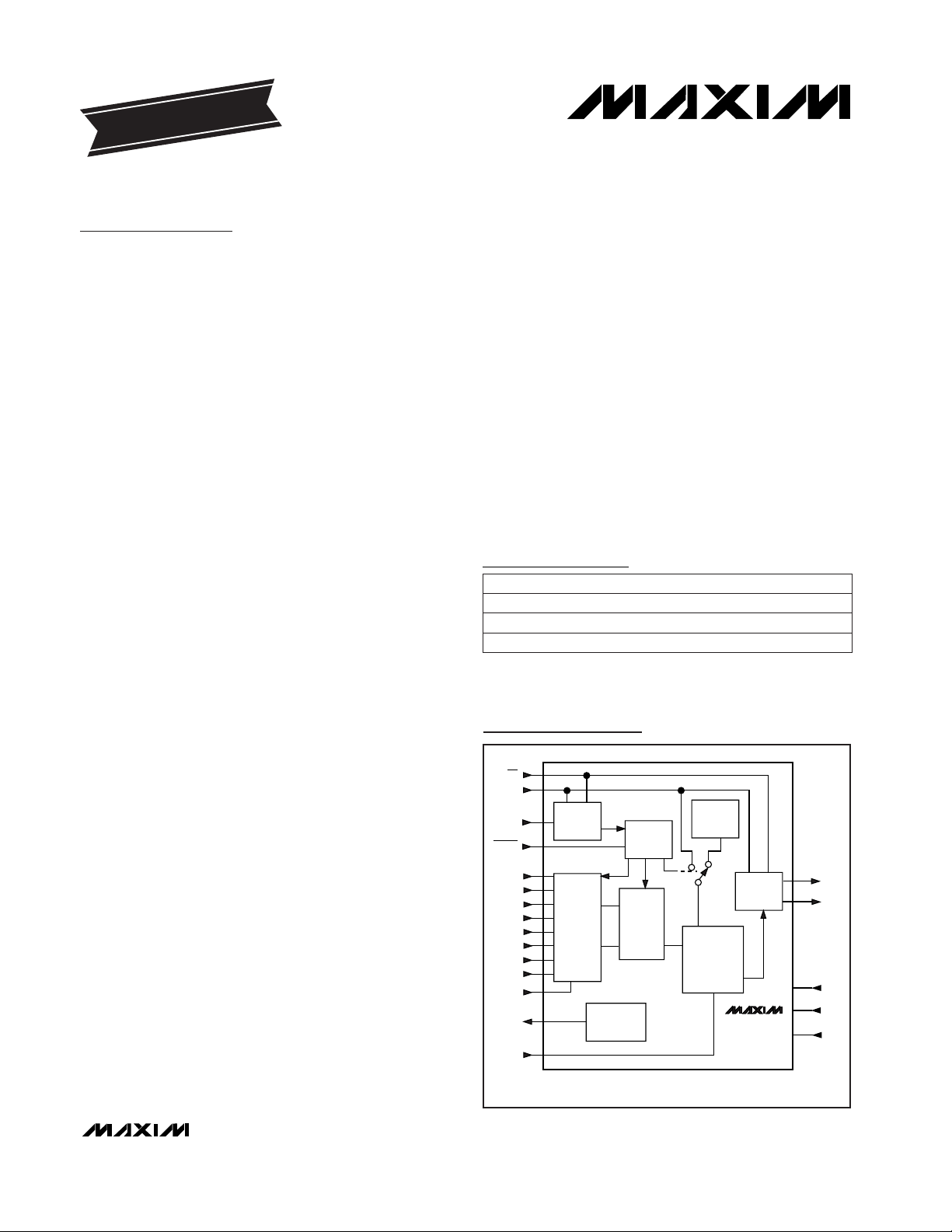
INPUT
SHIFT
REGISTER
CONTROL
LOGIC
INT
CLOCK
OUTPUT
SHIFT
REGISTER
+4.096V
REFERENCE
T/H
ANALOG
INPUT
MUX
8-BIT
SAR ADC
IN
DOUT
SSTRB
V
DD
DGND
AGND
SCLK
DIN
CH0
CH1
CH3
CH2
CH7*
CH6*
CH5*
CH4*
COM
REFOUT
*MAX1112 ONLY
REFIN
OUT
REF
CLOCK
MAX1112
MAX1113
CS
SHDN
Functional Diagram
19-1231; Rev 1; 10/98
PART
MAX1112CPP
MAX1112CAP 0°C to +70°C
0°C to +70°C
TEMP. RANGE PIN-PACKAGE
20 Plastic DIP
20 SSOP
EVALUATION KIT
AVAILABLE
Ordering Information
Ordering Information continued at end of data sheet.
*
Dice are specified at TA= +25°C, DC parameters only.
Pin Configurations appear at end of data sheet.
SPI and QSPI are trademarks of Motorola, Inc.
MICROWIRE is a trademark of National Semiconductor Corp.
MAX1112C/D 0°C to +70°C Dice*
For free samples & the latest literature: http://www.maxim-ic.com, or phone 1-800-998-8800.
For small orders, phone 1-800-835-8769.
Page 2
MAX1112/MAX1113
+5V, Low-Power, Multi-Channel,
Serial 8-Bit ADCs
2 _______________________________________________________________________________________
ABSOLUTE MAXIMUM RATINGS
Stresses beyond those listed under “Absolute Maximum Ratings” may cause permanent damage to the device. These are stress ratings only, and functional
operation of the device at these or any other conditions beyond those indicated in the operational sections of the specifications is not implied. Exposure to
absolute maximum rating conditions for extended periods may affect device reliability.
VDDto AGND..............................................................-0.3V to 6V
AGND to DGND.......................................................-0.3V to 0.3V
CH0–CH7, COM, REFIN,
REFOUT to AGND...................................-0.3V to (V
DD
+ 0.3V)
Digital Inputs to DGND...............................................-0.3V to 6V
Digital Outputs to DGND............................-0.3V to (V
DD
+ 0.3V)
Continuous Power Dissipation (T
A
= +70°C)
16 Plastic DIP (derate 10.53mW/°C above +70°C) ......842mW
16 QSOP (derate 8.30mW/°C above +70°C)................667mW
16 CERDIP (derate 10.00mW/°C above +70°C) ..........800mW
20 Plastic DIP (derate 11.11mW/°C above +70°C) ......889mW
20 SSOP (derate 8.00mW/°C above +70°C) ................640mW
20 CERDIP (derate 11.11mW/°C above +70°C) ..........889mW
Operating Temperature Ranges
MAX1112C_P/MAX1113C_E................................0°C to +70°C
MAX1112E_P/MAX1113E_E .............................-40°C to +85°C
MAX1112MJP/MAX1113MJE..........................-55°C to +125°C
Storage Temperature Range.............................-65°C to +150°C
Lead Temperature (soldering, 10sec).............................+300°C
ELECTRICAL CHARACTERISTICS
(VDD= +4.5V to +5.5V; unipolar input mode; COM = 0V; f
SCLK
= 500kHz, external clock (50% duty cycle); 10 clocks/conversion
cycle (50ksps); 1µF capacitor at REFOUT; T
A
= T
MIN
to T
MAX
; unless otherwise noted.)
-3dB rolloff MHz1.5Small-Signal Bandwidth
kHz800
V
CH_
= 4.096Vp-p, 25kHz (Note 3)
External reference, 4.096V
No missing codes over temperature
CONDITIONS
Full-Power Bandwidth
±1Internal or external reference LSBGain Error (Note 2)
dB-75Channel-to-Channel Crosstalk
dB68SFDRSpurious-Free Dynamic Range
dB-70THD
Total Harmonic Distortion
(up to the 5th harmonic)
LSB±0.1
Channel-to-Channel
Offset Matching
ppm/°C±0.8Gain Temperature Coefficient
LSB±1DNLDifferential Nonlinearity
UNITSMIN TYP MAXSYMBOLPARAMETER
MAX111_C/E LSB±0.3 ±1TUETotal Unadjusted Error
Bits8Resolution
dB49SINAD
Signal-to-Noise
and Distortion Ratio
LSB±0.1 ±0.5INLRelative Accuracy (Note 1)
LSB±0.3 ±1Offset Error
DC ACCURACY
DYNAMIC SPECIFICATIONS (10.034kHz sine-wave input, 4.096Vp-p, 50ksps, 500kHz external clock)
Page 3
µA
MAX1112/MAX1113
+5V, Low-Power, Multi-Channel,
Serial 8-Bit ADCs
_______________________________________________________________________________________ 3
ELECTRICAL CHARACTERISTICS (continued)
(VDD= +4.5V to +5.5V; unipolar input mode; COM = 0V; f
SCLK
= 500kHz, external clock (50% duty cycle); 10 clocks/conversion
cycle (50ksps); 1µF capacitor at REFOUT; T
A
= T
MIN
to T
MAX
; unless otherwise noted.)
On/off leakage current, V
CH_
= 0V or V
DD
Used for data transfer only
(Note 5)
External clock, 2MHz
CONDITIONS
ppm/°C±50
mA6REFOUT Short-Circuit Current
pF18Input Capacitance
µA±0.01 ±1Multiplexer Leakage Current
1
2
50 500
kHz400Internal Clock Frequency
0mA to 0.5mA output load mV4.5Load Regulation (Note 7)
ns10Aperture Delay
µs1t
ACQ
Track/Hold Acquisition Time
UNITSMIN TYP MAXSYMBOLPARAMETER
ps
V
1
V
DD
+
50mV
Input Voltage Range
(Note 8) µA120Input Current
<50Aperture Jitter
External clock, 500kHz, 10 clocks/conversion 20
Internal clock
µs
25 55
t
CONV
Conversion Time (Note 4)
Bipolar input, COM = V
REFIN
/ 2
Unipolar input, COM = 0V
COM ±
V
REFIN
/ 2
V
0V
REFIN
Input Voltage Range, SingleEnded and Differential (Note 6)
V3.936 4.096 4.256REFOUT Voltage
External Clock-Frequency Range
MHz
kHz
Capacitive Bypass at REFOUT µF
REFOUT Temperature Coefficient
V4.5 5.5V
DD
Supply Voltage
VDD= 4.5V to 5.5V; external reference,
4.096V; full-scale input
mV±0.4 ±4PSR
Power-Supply Rejection
(Note 9)
2
Power-down
3.2 10
Software
SHDN at DGND
Operating mode 135 250
Full-scale input
C
LOAD
= 10pF
Reference disabled 95
I
DD
µASupply Current
CONVERSION RATE
ANALOG INPUT
INTERNAL REFERENCE
EXTERNAL REFERENCE AT REFIN
POWER REQUIREMENTS
Page 4
MAX1112/MAX1113
+5V, Low-Power, Multi-Channel,
Serial 8-Bit ADCs
4 _______________________________________________________________________________________
ELECTRICAL CHARACTERISTICS (continued)
(VDD= +4.5V to +5.5V; unipolar input mode; COM = 0V; f
SCLK
= 500kHz, external clock (50% duty cycle); 10 clocks/conversion
cycle (50ksps); 1µF capacitor at REFOUT; T
A
= T
MIN
to T
MAX
; unless otherwise noted.)
CS = VDD(Note 5)
CS = V
DD
I
SOURCE
= 0.5mA
I
SINK
= 5mA
SHDN = open
SHDN = 0V or V
DD
(Note 5)
Digital inputs = 0V or V
DD
SHDN = open
CONDITIONS
pF15C
OUT
Three-State Output Capacitance
µA±0.01 ±10I
L
Three-State Leakage Current
VVDD- 0.5V
OH
Output High Voltage
V
0.4
V
OL
Output Low Voltage
nA±100
SHDN Maximum Allowed Leakage
for Mid-Input
VV
DD
/ 2V
FLT
SHDN Voltage, Floating
µA±4
SHDN Input Current
VV
DD
- 0.4V
SH
SHDN Input High Voltage
V0.8V
IL
DIN, SCLK, CS Input Low Voltage
V1.1 VDD- 1.1
I
SINK
= 16mA
V
SM
0.8
pF15C
IN
DIN, SCLK, CS Input Capacitance
µA±1I
IN
DIN, SCLK, CS Input Leakage
SHDN Input Mid-Voltage
V0.2V
HYST
DIN, SCLK, CS Input Hysteresis
UNITSMIN TYP MAXSYMBOLPARAMETER
V0.4V
SL
SHDN Input Low Voltage
VV
IH
DIN, SCLK, CS Input High Voltage
3
DIGITAL INPUTS: DIN, SCLK, CS
DIGITAL OUTPUTS: DOUT, SSTRB
SHDN INPUT
Page 5
MAX1112/MAX1113
+5V, Low-Power, Multi-Channel,
Serial 8-Bit ADCs
_______________________________________________________________________________________ 5
ns100t
CSS
Figure 1, external clock mode only,
C
LOAD
= 100pF
ns
CS to SCLK Rise Setup
240
Figure 1, C
LOAD
= 100pF ns
20 200
ns0t
CSH
CONDITIONS
CS to SCLK Rise Hold
240t
DV
CS Fall to Output Enable
Figure 2, C
LOAD
= 100pF ns240t
TR
CS Rise to Output Disable
t
SDV
CS Fall to SSTRB Output Enable
(Note 5)
Figure 2, external clock mode only,
C
LOAD
= 100pF
ns240t
STR
CS Rise to SSTRB Output
Disable (Note 5)
Figure 11, internal clock mode only ns0t
SCK
SSTRB Rise to SCLK Rise
(Note 5)
ns200t
CH
SCLK Pulse Width High
ns200t
CL
SCLK Pulse Width Low
C
LOAD
= 100pF ns240t
SSTRB
SCLK Fall to SSTRB
ns0t
DH
DIN to SCLK Hold
µs1t
ACQ
Track/Hold Acquisition Time
ns100t
DS
DIN to SCLK Setup
UNITSMIN TYP MAXSYMBOLPARAMETER
TIMING CHARACTERISTICS (Figures 8 and 9)
(VDD= +4.5V to +5.5V, TA= T
MIN
to T
MAX
, unless otherwise noted.)
Note 1: Relative accuracy is the analog value’s deviation (at any code) from its theoretical value after the full-scale range is calibrated.
Note 2: V
REFIN
= 4.096V, offset nulled.
Note 3: On-channel grounded; sine wave applied to all off-channels.
Note 4: Conversion time is defined as the number of clock cycles multiplied by the clock period; clock has 50% duty cycle.
Note 5: Guaranteed by design. Not subject to production testing.
Note 6: Common-mode range for the analog inputs is from AGND to V
DD
.
Note 7: External load should not change during the conversion for specified accuracy.
Note 8: External reference at 4.096V, full-scale input, 500kHz external clock.
Note 9: Measured as
| V
FS
(4.5V) - VFS(5.5V) |.
Note 10: 1µF at REFOUT; internal reference settling to 0.5LSB.
ns
20 240
t
DO
SCLK Fall to Output Data Valid
Figure 1,
C
LOAD
= 100pF
MAX111_C/E
MAX111_M
External reference 20
Internal reference (Note 10)
µs
24
t
WAKE
Wakeup Time
ms
Page 6
MAX1112/MAX1113
+5V, Low-Power, Multi-Channel,
Serial 8-Bit ADCs
6 _______________________________________________________________________________________
__________________________________________Typical Operating Characteristics
(VDD= +5.0V; f
SCLK
= 500kHz; external clock (50% duty cycle); RL= ∞; TA = +25°C, unless otherwise noted.)
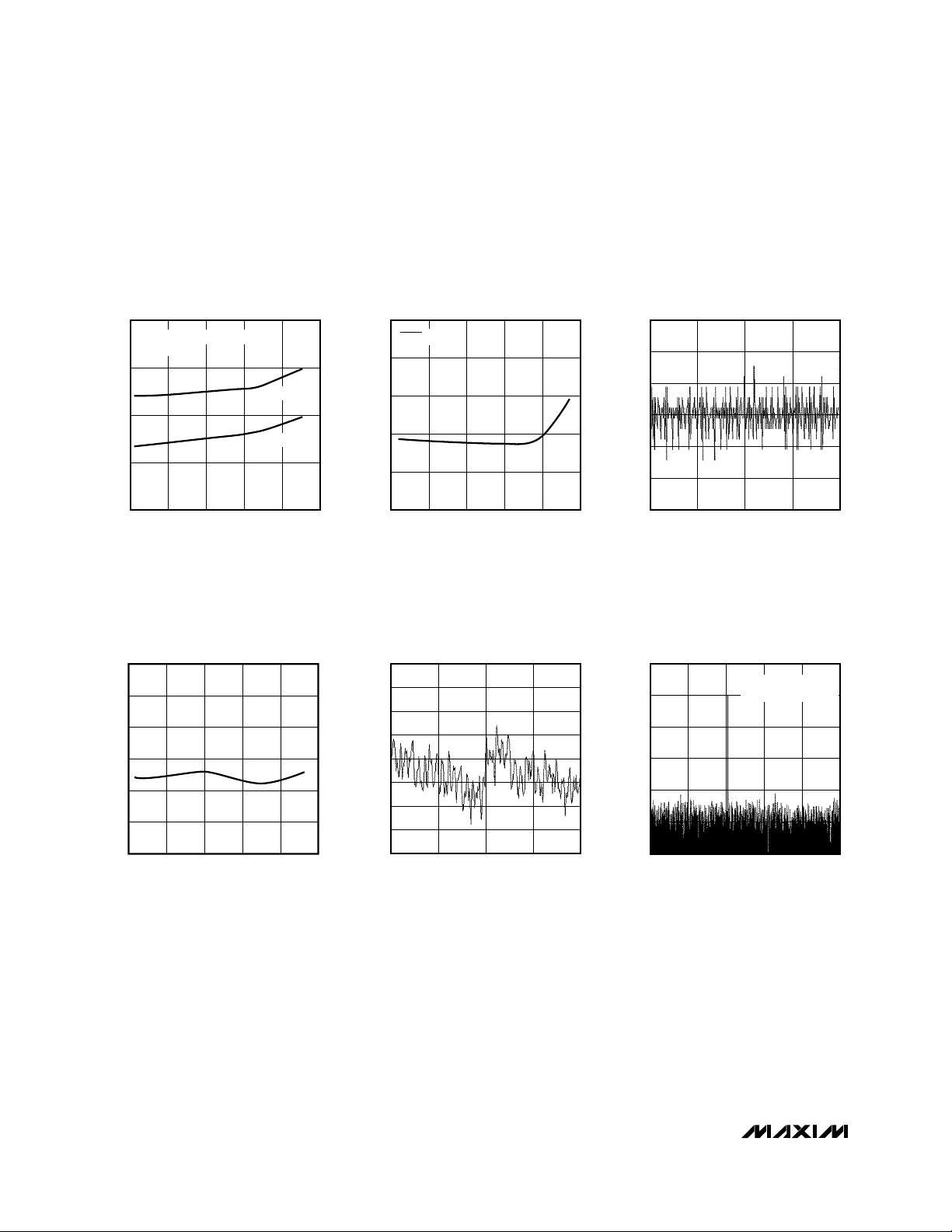
180
100
-60 140
SUPPLY CURRENT vs. TEMPERATURE
120
MAX1112/13-01
TEMPERATURE (°C)
SUPPLY CURRENT (µA)
-20 20 60 100
160
140
OUTPUT CODE = FULL SCALE
C
LOAD
= 10pF
VDD = 5.5V
VDD = 4.5V
10
0
-60 140
SHUTDOWN SUPPLY CURRENT
vs. TEMPERATURE
2
8
MAX1112/13-02
TEMPERATURE (°C)
SHUTDOWN SUPPLY CURRENT (µA)
-20 20 60 100
6
4
SHDN = DGND
0.3
-0.3
0 256
DIFFERENTIAL NONLINEARITY
vs. CODE
-0.2
0.2
0.1
MAX1112/13-03
DIGITAL CODE
DNL (LSB)
64 128 192
0
-0.1
0.6
0
-60 140
OFFSET ERROR vs. TEMPERATURE
0.1
0.2
0.5
MAX1112/13-04
TEMPERATURE (°C)
OFFSET ERROR (LSB)
-20 20 60
100
0.4
0.3
0.20
-0.20
0 256
INTEGRAL NONLINEARITY
vs. CODE
-0.10
-0.15
0.15
0.10
0.05
MAX1112/13-05
DIGITAL CODE
INL (LSB)
64 128 192
0
-0.05
20
-100
025
FFT PLOT
-80
-20
0
MAX1112/13-06
FREQUENCY (kHz)
AMPLITUDE (dB)
5 101520
-60
-40
f
CH_
= 10.034kHz, 4Vp-p
f
SAMPLE
= 50ksps
Page 7

MAX1112/MAX1113
+5V, Low-Power, Multi-Channel,
Serial 8-Bit ADCs
_______________________________________________________________________________________ 7
Pin Description
16 SSTRB
Serial-Strobe Output. In internal clock mode, SSTRB goes low when the MAX1112/
MAX1113 begin the A/D conversion and goes high when the conversion is complete.
In external clock mode, SSTRB pulses high for two clock periods before the MSB is
shifted out. High impedance when CS is high (external clock mode only).
20 V
DD
Positive Supply Voltage, +4.5V to +5.5V
18
CS
Active-Low Chip Select. Data is not clocked into DIN unless CS is low. When CS is
high, DOUT is high impedance.
19 SCLK
Serial-Clock Input. Clocks data in and out of serial interface. In external clock mode,
SCLK also sets the conversion speed (duty cycle must be 45% to 55%).
17 DIN Serial-Data Input. Data is clocked in at SCLK’s rising edge.
12 REFOUT Internal Reference Generator Output. Bypass with a 1µF capacitor to AGND.
14 DGND Digital Ground
15 DOUT
Serial-Data Output. Data is clocked out on SCLK’s falling edge. High impedance when
CS is high.
13 AGND Analog Ground
10
SHDN
Three-Level Shutdown Input. Normally floats. Pulling SHDN low shuts the MAX1112/
MAX1113 down to 10µA (max) supply current; otherwise, the devices are fully operational. Pulling SHDN high shuts down the internal reference.
11 REFIN
Reference Voltage Input for Analog-to-Digital Conversion. Connect to REFOUT to use
the internal reference.
5–8 CH4–CH7 Sampling Analog Inputs
1–4 CH0–CH3 Sampling Analog Inputs
+5V
3k
C
LOAD
DGND
DOUT
C
LOAD
DGND
3k
DOUT
a) High-Z to V
OH
and VOL to V
OH
b) High-Z to VOL and VOH to V
OL
Figure 1. Load Circuits for Enable Time
+5V
3k
C
LOAD
DGND
DOUT
C
LOAD
DGND
3k
DOUT
a) V
OH
to High-Z b) VOL to High-Z
Figure 2. Load Circuits for Disable Time
12
16
14
15
13
8
10
11
9
6
7
—
1–4
59 COM
Ground Reference for Analog Inputs. Sets zero-code voltage in single-ended mode.
Must be stable to ±0.5LSB.
PIN
MAX1113
NAME FUNCTION
MAX1112
Page 8

MAX1112/MAX1113
+5V, Low-Power, Multi-Channel,
Serial 8-Bit ADCs
8 _______________________________________________________________________________________
_______________Detailed Description
The MAX1112/MAX1113 analog-to-digital converters
(ADCs) use a successive-approximation conversion
technique and input track/hold (T/H) circuitry to convert
an analog signal to an 8-bit digital output. A flexible serial interface provides easy interface to microprocessors
(µPs). Figure 3 shows the Typical Operating Circuit.
Pseudo-Differential Input
The sampling architecture of the ADC’s analog comparator is illustrated in Figure 4, the equivalent input circuit. In single-ended mode, IN+ is internally switched to
the selected input channel, CH_, and IN- is switched to
COM. In differential mode, IN+ and IN- are selected
from the following pairs: CH0/CH1, CH2/CH3,
CH4/CH5, and CH6/CH7. Configure the MAX1112
channels with Table 1 and the MAX1113 channels with
Table 2.
In differential mode, IN- and IN+ are internally switched
to either of the analog inputs. This configuration is
pseudo-differential to the effect that only the signal at
IN+ is sampled. The return side (IN-) must remain stable within ±0.5LSB (±0.1LSB for best results) with
respect to AGND during a conversion. To accomplish
this, connect a 0.1µF capacitor from IN- (the selected
analog input) to AGND if necessary.
During the acquisition interval, the channel selected as
the positive input (IN+) charges capacitor C
HOLD
. The
acquisition interval spans two SCLK cycles and ends
on the falling SCLK edge after the last bit of the input
control word has been entered. At the end of the acquisition interval, the T/H switch opens, retaining charge
on C
HOLD
as a sample of the signal at IN+.
The conversion interval begins with the input multiplexer switching C
HOLD
from the positive input (IN+) to the
negative input (IN-). In single-ended mode, IN- is simply COM. This unbalances node ZERO at the input of
the comparator. The capacitive DAC adjusts during the
remainder of the conversion cycle to restore node
ZERO to 0V within the limits of 8-bit resolution. This
action is equivalent to transferring a charge of 18pF x
(V
IN+
- V
IN-
) from C
HOLD
to the binary-weighted capacitive DAC, which in turn forms a digital representation of
the analog input signal.
Track/Hold
The T/H enters its tracking mode on the falling clock
edge after the sixth bit of the 8-bit control byte has
been shifted in. It enters its hold mode on the falling
clock edge after the eighth bit of the control byte has
been shifted in. If the converter is set up for singleended inputs, IN- is connected to COM, and the converter samples the “+” input; if it is set up for differential
inputs, IN- connects to the “-” input, and the difference
(IN+ - IN-) is sampled. At the end of the conversion, the
positive input connects back to IN+, and C
HOLD
charges to the input signal.
V
DD
I/O
SCK (SK)
MOSI (SO)
MISO (SI)
V
SS
SHDN
SSTRB
DOUT
DIN
SCLK
CS
COM
DGND
AGND
V
DD
CH7
1µF
0.1µF
1µF
CH0
ANALOG
INPUTS
MAX1112
MAX1113
CPU
+5V
REFIN
REFOUT
Figure 3. Typical Operating Circuit
CH0
CH1
CH2
CH3
CH4*
CH5*
CH6*
CH7*
COM
C
SWITCH
TRACK
T/H
SWITCH
C
HOLD
HOLD
CAPACITIVE DAC
REFIN
ZERO
COMPARATOR
–
+
18pF
6.5k
R
IN
SINGLE-ENDED MODE: IN+ = CHO–CH7, IN- = COM.
DIFFERENTIAL MODE: IN+ AND IN- SELECTED FROM PAIRS OF
CH0/CH1, CH2/CH3, CH4*/CH5*, CH6*/CH7*.
*MAX1112 ONLY
AT THE SAMPLING INSTANT,
THE MUX INPUT SWITCHES
FROM THE SELECTED IN+
CHANNEL TO THE SELECTED
IN- CHANNEL.
INPUT
MUX
Figure 4. Equivalent Input Circuit
Page 9

MAX1112/MAX1113
+5V, Low-Power, Multi-Channel,
Serial 8-Bit ADCs
_______________________________________________________________________________________ 9
Table 1a. MAX1112 Channel Selection in Single-Ended Mode (SGL/DIF = 1)
Table 1b. MAX1112 Channel Selection in Differential Mode (SGL/DIF = 0)
Table 2a. MAX1113 Channel Selection in Single-Ended Mode (SGL/DIF = 1)
Table 2b. MAX1113 Channel Selection in Differential Mode (SGL/DIF = 0)
–+
111
–+
1
CH2
10
–+
0
CH3
11
–+
0
CH1
10
+ –
1
+
CH0
01
+ –
100
+ –
001
–
COMCH7CH6SEL2 CH5CH4
000
SEL0SEL1
+–
111
+–
0
CH2
11
– +
1
CH3
01
+–
0
–
CH1
01
–+
1
+
CH0
10
–+
010
+ –
100
CH7CH6SEL2 CH5CH4
000
SEL0SEL1
+
X11
+
X
CH1
10
+
CH0
+
X01
SEL2 CH3CH2
X00
SEL0SEL1
+–
X11
+–
X
–
CH1
01
+
CH0
–+
X10
SEL2 CH3CH2
X00
SEL0SEL1
–
–
–
–
COM
Page 10

MAX1112/MAX1113
+5V, Low-Power, Multi-Channel,
Serial 8-Bit ADCs
10 ______________________________________________________________________________________
Table 3. Control-Byte Format
START SEL2 SEL1 SEL0 UNI/BIP SGL/DIF PD1 PD0
BIT 7 BIT 6 BIT 5 BIT 4 BIT 3 BIT 2 BIT 1 BIT 0
(MSB) (LSB)
NAME
SGL/DIF
2
BIT
1 = single ended, 0 = differential. Selects single-ended or differential conversions. In single-
ended mode, input signal voltages are referred to COM. In differential mode, the voltage difference between two channels is measured. See Tables 1 and 2.
DESCRIPTION
UNI/BIP
3
START
1 = unipolar, 0 = bipolar. Selects unipolar or bipolar conversion mode (Table 4).
PD00 (LSB)
7 (MSB)
1 = external clock mode, 0 = internal clock mode.
Selects external or internal clock mode.
The first logic “1” bit after CS goes low defines the beginning of the control byte.
SEL2
SEL1
SEL0
6
5
4
Select which of the input channels are to be used for the conversion (Tables 1 and 2).
PD11
1 = fully operational, 0 = power-down.
Selects fully operational or power-down mode.
The time required for the T/H to acquire an input signal
is a function of how quickly its input capacitance is
charged. If the input signal’s source impedance is high,
the acquisition time lengthens, and more time must be
allowed between conversions. The acquisition time,
t
ACQ
, is the minimum time needed for the signal to be
acquired. It is calculated by:
t
ACQ
= 6 x (RS+ RIN) x 18pF
where RIN= 6.5kΩ, RS= the source impedance of the
input signal, and t
ACQ
is never less than 1µs. Note that
source impedances below 2.4kΩ do not significantly
affect the AC performance of the ADC.
Input Bandwidth
The ADC’s input tracking circuitry has a 1.5MHz smallsignal bandwidth, so it is possible to digitize highspeed transient events and measure periodic signals
with bandwidths exceeding the ADC’s sampling rate by
using undersampling techniques. To avoid highfrequency signals being aliased into the frequency
band of interest, anti-alias filtering is recommended.
Analog Inputs
Internal protection diodes, which clamp the analog
input to VDDand AGND, allow the channel input pins to
swing from (AGND - 0.3V) to (VDD+ 0.3V) without dam-
age. However, for accurate conversions near full scale,
the inputs must not exceed V
DD
by more than 50mV or
be lower than AGND by 50mV.
If the analog input exceeds 50mV beyond the supplies, do not forward bias the protection diodes of
off channels over 2mA.
The MAX1112/MAX1113 can be configured for differential or single-ended inputs with bits 2 and 3 of the control byte (Table 3). In single-ended mode, analog inputs
are internally referenced to COM with a full-scale input
range from COM to V
REFIN
+ COM. For bipolar opera-
tion, set COM to V
REFIN
/ 2.
In differential mode, choosing unipolar mode sets the
differential input range at 0V to V
REFIN
. In unipolar
mode, the output code is invalid (code zero) when a
negative differential input voltage is applied. Bipolar
mode sets the differential input range to ±V
REFIN
/ 2.
Note that in this mode, the common-mode input range
includes both supply rails. Refer to Table 4 for input
voltage ranges.
Quick Look
To quickly evaluate the MAX1112/MAX1113’s analog
performance, use the circuit of Figure 5. The
MAX1112/MAX1113 require a control byte to be written
to DIN before each conversion. Tying DIN to +5V feeds
Page 11

MAX1112/MAX1113
+5V, Low-Power, Multi-Channel,
Serial 8-Bit ADCs
______________________________________________________________________________________ 11
in control bytes of $FF (hex), which trigger singleended, unipolar conversions on CH7 (MAX1112) or
CH3 (MAX1113) in external clock mode without powering down between conversions. In external clock mode,
the SSTRB output pulses high for two clock periods
before the most significant bit (MSB) of the 8-bit conversion result is shifted out of DOUT. Varying the analog input alters the output code. A total of 10 clock
cycles is required per conversion. All transitions of the
SSTRB and DOUT outputs occur on SCLK’s falling
edge.
How to Start a Conversion
A conversion is started by clocking a control byte into
DIN. With CS low, each rising edge on SCLK clocks a bit
from DIN into the MAX1112/MAX1113’s internal shift register. After CS falls, the first arriving logic “1” bit at DIN
defines the MSB of the control byte. Until this first start bit
arrives, any number of logic “0” bits can be clocked into
DIN with no effect. Table 3 shows the control-byte format.
The MAX1112/MAX1113 are compatible with
MICROWIRE, SPI, and QSPI devices. For SPI, select the
correct clock polarity and sampling edge in the SPI control registers: set CPOL = 0 and CPHA = 0. MICROWIRE,
SPI, and QSPI all transmit a byte and receive a byte at the
same time. Using the Typical Operating Circuit (Figure 3),
the simplest software interface requires three 8-bit transfers to perform a conversion (one 8-bit transfer to configure the ADC, and two more 8-bit transfers to clock out the
1µF
0.1µF
V
DD
DGND
AGND
CS
SCLK
DIN
DOUT
SSTRB
SHDN
+5V
N.C.
0.01µF
CH7 (CH3)
COM
REFOUT
REFIN
C1
1µF
0V TO
+4.096V
ANALOG
INPUT
OSCILLOSCOPE
CH1 CH2
CH3
CH4
*FULL-SCALE ANALOG INPUT, CONVERSION RESULT = $FF (HEX)
( ) ARE FOR THE MAX1113.
MAX1112
MAX1113
+5V
500kHz
OSCILLATOR
SCLK
SSTRB
DOUT*
Figure 5. Quick-Look Circuit
Table 4. Full-Scale and Zero-Scale Voltages
UNIPOLAR MODE
V
REFIN
+ COM
+V
REFIN
/ 2
+ COM
Full Scale
COM COM
-V
REFIN
/ 2
+ COM
Positive
Full Scale
Zero Scale
Zero
Scale
BIPOLAR MODE
Negative
Full Scale
Page 12

8-bit conversion result). Figure 6 shows the MAX1112/
MAX1113 common serial-interface connections.
Simple Software Interface
Make sure the CPU’s serial interface runs in master
mode so the CPU generates the serial clock. Choose a
clock frequency from 50kHz to 500kHz.
1) Set up the control byte for external clock mode and
call it TB1. TB1 should be of the format 1XXXXX11
binary, where the Xs denote the particular channel
and conversion mode selected.
2) Use a general-purpose I/O line on the CPU to pull
CS low.
3) Transmit TB1 and, simultaneously, receive a byte
and call it RB1. Ignore RB1.
4) Transmit a byte of all zeros ($00 hex) and, simultaneously, receive byte RB2.
5) Transmit a byte of all zeros ($00 hex) and, simultaneously, receive byte RB3.
6) Pull CS high.
Figure 7 shows the timing for this sequence. Bytes RB2
and RB3 contain the result of the conversion padded
with two leading zeros and six trailing zeros. The total
conversion time is a function of the serial-clock
frequency and the amount of idle time between 8-bit
transfers. Make sure that the total conversion time does
not exceed 1ms, to avoid excessive T/H droop.
MAX1112/MAX1113
+5V, Low-Power, Multi-Channel,
Serial 8-Bit ADCs
12 ______________________________________________________________________________________
SSTRB
CS
SCLK
DIN
DOUT
14 8 12 16 20 24
START
SEL2 SEL1 SEL0
UNI/
BIP
SGL/
DIF
PD1 PD0
B7 B6 B5 B4 B3 B2 B1 B0
ACQUISITION
(f
SCLK
= 500kHz)
IDLE
FILLED WITH ZEROS
IDLE
CONVERSION
t
ACQ
A/D STATE
RB1
RB2
RB3
4µs
Figure 7. Single-Conversion Timing, External Clock Mode, 24 Clocks
CS
SCLK
DOUT
I/O
SCK
MISO
+5V
SS
a) SPI
CS
SCLK
DOUT
CS
SCK
MISO
+5V
SS
b) QSPI
MAX1112
MAX1113
MAX1112
MAX1113
MAX1112
MAX1113
CS
SCLK
DOUT
I/O
SK
SI
c) MICROWIRE
Figure 6. Common Serial-Interface Connections to the
MAX1112/MAX1113
Page 13

MAX1112/MAX1113
+5V, Low-Power, Multi-Channel,
Serial 8-Bit ADCs
______________________________________________________________________________________ 13
Digital Output
In unipolar input mode, the output is straight binary
(Figure 15). For bipolar inputs, the output is two’s-complement (Figure 16). Data is clocked out at SCLK’s
falling edge in MSB-first format.
Clock Modes
The MAX1112/MAX1113 can use either an external serial clock or the internal clock to perform the successiveapproximation conversion. In both clock modes, the
external clock shifts data in and out of the devices. Bit
PD0 of the control byte programs the clock mode.
Figures 8–11 show the timing characteristics common
to both modes.
External Clock
In external clock mode, the external clock not only
shifts data in and out, it also drives the analog-to-digital
conversion steps. SSTRB pulses high for two clock
periods after the last bit of the control byte. Successiveapproximation bit decisions are made and appear at
DOUT on each of the next eight SCLK falling edges
(Figure 7). After the eight data bits are clocked out,
subsequent clock pulses clock out zeros from the
DOUT pin.
SSTRB and DOUT go into a high-impedance state
when CS goes high; after the next CS falling edge,
SSTRB outputs a logic low. Figure 9 shows the SSTRB
timing in external clock mode.
The conversion must complete in 1ms, or droop on the
sample-and-hold capacitors may degrade conversion
results. Use internal clock mode if the serial-clock frequency is less than 50kHz, or if serial-clock interruptions
could cause the conversion interval to exceed 1ms.
• • •
• • •
• • •
• • •
CS
SCLK
DIN
DOUT
t
CSS
t
CL
t
DS
t
DH
t
DV
t
DO
t
CH
t
DO
t
TR
t
CSH
Figure 8. Detailed Serial-Interface Timing
• • •
• • •
• • •
• • • •
• • •
t
SDV
t
SSTRB
PD0 CLOCKED IN
t
STR
SSTRB
SCLK
CS
t
SSTRB
• • • •
Figure 9. External Clock Mode SSTRB Detailed Timing
Page 14
MAX1112/MAX1113
+5V, Low-Power, Multi-Channel,
Serial 8-Bit ADCs
14 ______________________________________________________________________________________
SSTRB
CS
SCLK
DIN
DOUT
14 8
12
15
17
START
SEL2 SEL1 SEL0
UNI/
BIP
SGL/
DIF
PD1 PD0
B7 B6 B1
B0
t
ACQ
4µs (f
SCLK
= 500kHz)
IDLE
FILLED WITH
ZEROS
IDLE
CONVERSION
25µs TYP
A/D STATE
2 3 5 6 7 9 10 11 16 18
t
CONV
Figure 10. Internal Clock Mode Timing
PD0 CLOCK IN
t
SSTRB
t
CSH
t
CONV
t
SCK
SSTRB
SCLK
t
CSS
NOTE: FOR BEST NOISE PERFORMANCE, KEEP SCLK LOW DURING CONVERSION.
CS
Figure 11. Internal Clock Mode SSTRB Detailed Timing
Internal Clock
Internal clock mode frees the µP from the burden of
running the SAR conversion clock. This allows the conversion results to be read back at the processor’s convenience, at any clock rate up to 2MHz. SSTRB goes
low at the start of the conversion and then goes high
when the conversion is complete. SSTRB is low for
25µs (typically), during which time SCLK should remain
low for best noise performance.
An internal register stores data when the conversion is
in progress. SCLK clocks the data out of this register at
any time after the conversion is complete. After SSTRB
goes high, the second falling clock edge produces the
MSB of the conversion at DOUT, followed by the
remaining bits in MSB-first format (Figure 10). CS does
not need to be held low once a conversion is started.
Pulling CS high prevents data from being clocked into
the MAX1112/MAX1113 and three-states DOUT, but it
does not adversely affect an internal clock-mode conversion already in progress. When internal clock mode
is selected, SSTRB does not go into a high-impedance
state when CS goes high.
Figure 11 shows the SSTRB timing in internal clock
mode. In this mode, data can be shifted in and out of
the MAX1112/MAX1113 at clock rates up to 2MHz, provided that the minimum acquisition time, t
ACQ
, is kept
above 1µs.
Page 15

MAX1112/MAX1113
+5V, Low-Power, Multi-Channel,
Serial 8-Bit ADCs
______________________________________________________________________________________ 15
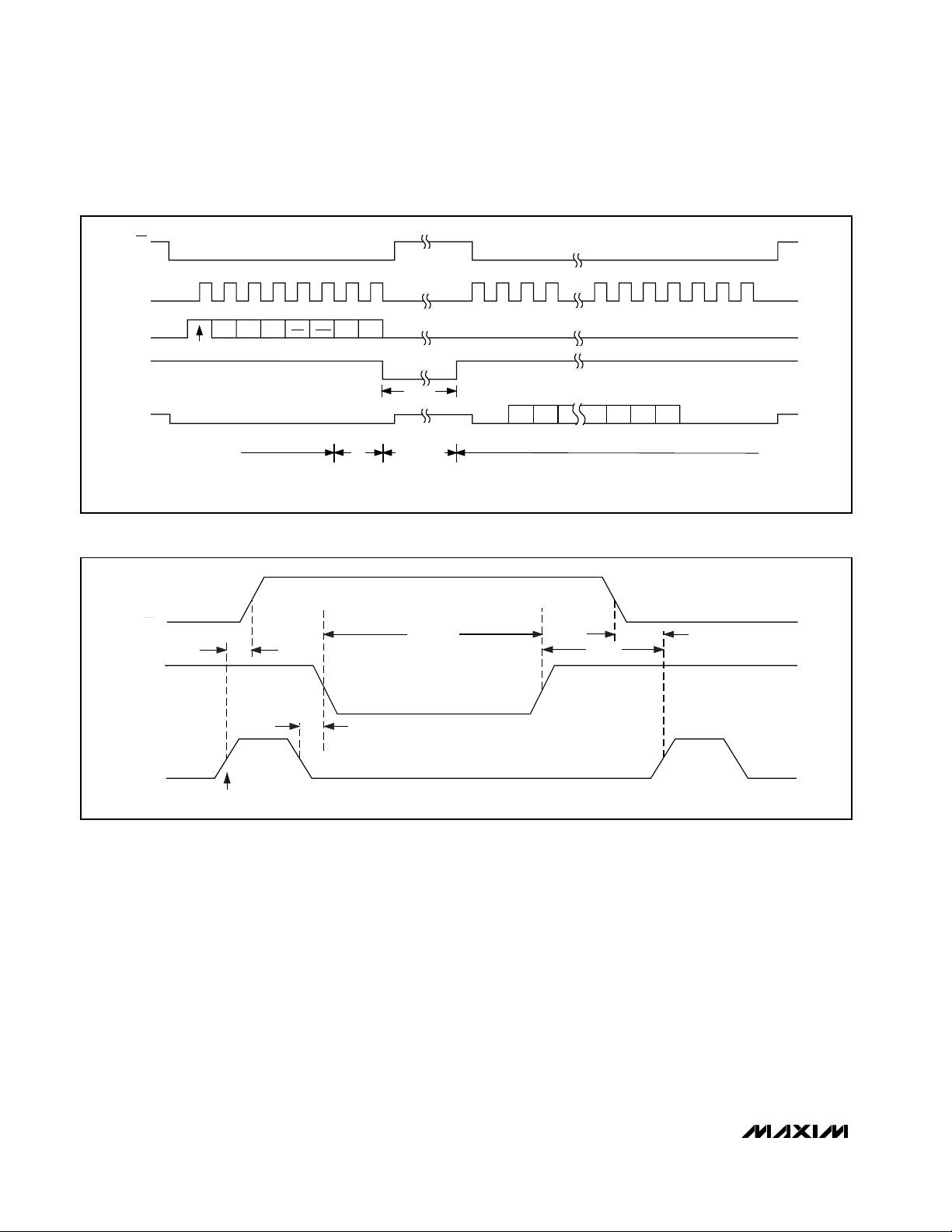
SCLK
DIN
DOUT
CS
S CONTROL BYTE 0
CONTROL BYTE 1S
CONVERSION RESULT 0
B7 B0 B7 B0
B7
CONVERSION RESULT 1 CONVERSION RESULT 2
SSTRB
CONTROL BYTE 2S
1
88810 1 10
1
10 1
CONTROL BYTE 3S
Figure 12a. Continuous Conversions, External Clock Mode, 10 Clocks/Conversion Timing
CS
SCLK
DIN
DOUT
S CONTROL BYTE 0
CONTROL BYTE 1S
CONVERSION RESULT 0
B7 B0
B7
CONVERSION RESULT 1
Figure 12b. Continuous Conversions, External Clock Mode, 16 Clocks/Conversion Timing
Data Framing
The falling edge of CS does not start a conversion. The
first logic high clocked into DIN is interpreted as a start
bit and defines the first bit of the control byte. A conversion starts on the falling edge of SCLK, after the eighth
bit of the control byte (the PD0 bit) is clocked into DIN.
The start bit is defined as:
The first high bit clocked into DIN with CS low any
time the converter is idle, e.g., after VDDis applied.
OR
The first high bit clocked into DIN after the MSB of a
conversion in progress is clocked onto the DOUT
pin.
If CS is toggled before the current conversion is complete, then the next high bit clocked into DIN is recognized as a start bit; the current conversion is
terminated, and a new one is started.
The fastest the MAX1112/MAX1113 can run is 10
clocks per conversion. Figure 12a shows the serialinterface timing necessary to perform a conversion
every 10 SCLK cycles in external clock mode.
Many microcontrollers require that conversions occur in
multiples of eight SCLK clocks; 16 clocks per conversion is typically the fastest that a microcontroller can
drive the MAX1112/MAX1113. Figure 12b shows the
serial-interface timing necessary to perform a conversion every 16 SCLK cycles in external clock mode.
Page 16
__________Applications Information
Power-On Reset
When power is first applied, and if SHDN is not pulled
low, internal power-on reset circuitry activates the
MAX1112/MAX1113 in internal clock mode. SSTRB is
high on power-up and, if CS is low, the first logical 1 on
DIN is interpreted as a start bit. Until a conversion takes
place, DOUT shifts out zeros. No conversions should
be performed until the reference voltage has stabilized
(see the Wakeup Time specifications in the
Timing
Characteristics
).
Power-Down
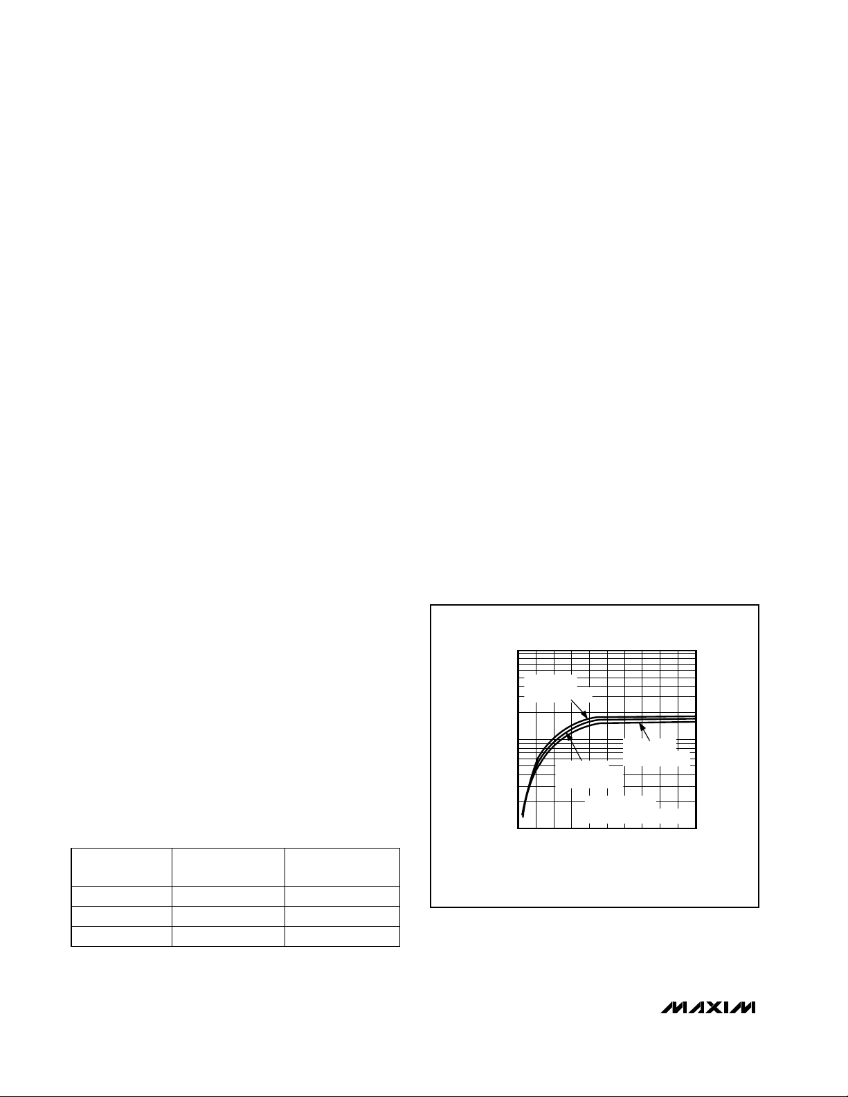
When operating at speeds below the maximum sampling rate, the MAX1112/MAX1113’s automatic powerdown mode can save considerable power by placing
the converters in a low-current shutdown state between
conversions. Figure 13 shows the average supply current as a function of the sampling rate.
Select power-down with PD1 of the DIN control byte
with SHDN high or floating (Table 3). Pull SHDN low at
any time to shut down the converters completely. SHDN
overrides PD1 of the control byte. Figures 14a and 14b
illustrate the various power-down sequences in both
external and internal clock modes.
Software Power-Down
Software power-down is activated using bit PD1 of the
control byte. When software power-down is asserted, the
ADCs continue to operate in the last specified clock
mode until the conversion is complete. The ADCs then
power down into a low quiescent-current state. In internal
clock mode, the interface remains active, and conversion
results may be clocked out after the MAX1112/
MAX1113 have entered a software power-down.
The first logical 1 on DIN is interpreted as a start bit,
which powers up the MAX1112/MAX1113. If the DIN byte
contains PD1 = 1, then the chip remains powered up. If
PD1 = 0, power-down resumes after one conversion.
Hard-Wired Power-Down
Pulling SHDN low places the converters in hard-wired
power-down. Unlike software power-down, the conversion is not completed; it stops coincidentally with SHDN
being brought low. SHDN also controls the state of the
internal reference (Table 5). Letting SHDN float enables
the internal 4.096V voltage reference. When returning to
normal operation with SHDN floating, there is a t
RC
delay of approximately 1MΩ x C
LOAD
, where C
LOAD
is
the capacitive loading on the SHDN pin. Pulling SHDN
high disables the internal reference, which saves power
when using an external reference.
External Reference
An external reference between 1V and VDDshould be
connected directly at the REFIN terminal. The DC input
impedance at REFIN is extremely high, consisting of
leakage current only (typically 10nA). During a conversion, the reference must be able to deliver up to 20µA
average load current and have an output impedance of
1kΩ or less at the conversion clock frequency. If the
reference has higher output impedance or is noisy,
bypass it close to the REFIN pin with a 0.1µF capacitor.
If an external reference is used with the MAX1112/
MAX1113, tie SHDN to VDDto disable the internal reference and decrease power consumption.
MAX1112/MAX1113
+5V, Low-Power, Multi-Channel,
Serial 8-Bit ADCs
16 ______________________________________________________________________________________
Table 5. Hard-Wired Power-Down and
Internal Reference State
SHDN
STATE
DEVICE
MODE
1 Enabled
Floating Enabled
0 Power-Down
INTERNAL
REFERENCE
Disabled
Disabled
Enabled
Figure 13. Average Supply Current vs. Sampling Rate
1000
C
= 60pF
LOAD
CODE = 10101010
100
C
= 30pF
SUPPLY CURRENT (µA)
10
010 30 50
LOAD
CODE = 10101010
SAMPLING RATE (ksps)
C
= 30pF
LOAD
CODE = 11111111
VDD = V
C
20 40
REFIN
AT DOUT + SSTRB
LOAD
= 5V
MAX1112/13-fig13
Page 17

MAX1112/MAX1113
+5V, Low-Power, Multi-Channel,
Serial 8-Bit ADCs
______________________________________________________________________________________ 17
Internal Reference
To use the MAX1112/MAX1113 with the internal reference, connect REFIN to REFOUT. The full-scale range
of the MAX1112/MAX1113 with the internal reference is
typically 4.096V with unipolar inputs, and ±2.048V with
bipolar inputs. The internal reference should be
bypassed to AGND with a 1µF capacitor placed as
close to the REFIN pin as possible.
Transfer Function
Table 4 shows the full-scale voltage ranges for unipolar
and bipolar modes. Figure 15 depicts the nominal,
unipolar I/O transfer function, and Figure 16 shows the
bipolar I/O transfer function when using a 4.096V reference. Code transitions occur at integer LSB values.
Output coding is binary, with 1LSB = 16mV
(4.096V/256) for unipolar operation and 1LSB = 16mV
[(4.096V/2 - -4.096V/2)/256] for bipolar operation.
POWERED UP
POWER-
DOWN
POWERED
UP
POWERED UP
DATA VALID
DATA VALID DATA
INVALID
EXTERNALEXTERNAL
INTERNAL
SX
XXXX
11 S 01
XXXXX XXXXX
S11
POWER-
DOWN
MODE
DOUT
DIN
CLOCK
MODE
SHDN
SETS EXTERNAL
CLOCK MODE
SETS EXTERNAL
CLOCK MODE
SETS POWERDOWN MODE
Figure 14a. Power-Down Modes, External Clock Timing Diagram
POWER-DOWN
POWERED
UP
POWERED UP
DATA VALID
DATA VALID
INTERNAL CLOCK MODE
SX
XXXX
10 S 00
XXXXX
S
MODE
DOUT
DIN
SETS INTERNAL
CLOCK MODE
SETS POWER-DOWN MODE
CONVERSION
CONVERSION
SSTRB
Figure 14b. Power-Down Modes, Internal Clock Timing Diagram
Page 18

Layout, Grounding, and Bypassing
For best performance, use printed circuit boards. Wirewrap boards are not recommended. Board layout
should ensure that digital and analog signal lines are
separated from each other. Do not run analog and digital (especially clock) lines parallel to one another, or
digital lines underneath the ADC package.
Figure 17 shows the recommended system ground
connections. A single-point analog ground (star ground
point) should be established at AGND, separate from
the logic ground. Connect all other analog grounds and
DGND to the star ground. No other digital system
ground should be connected to this ground. The
ground return to the power supply for the star ground
should be low impedance and as short as possible for
noise-free operation.
High-frequency noise in the VDDpower supply may
affect the comparator in the ADC. Bypass the supply to
the star ground with 0.1µF and 1µF capacitors close to
the VDDpin of the MAX1112/MAX1113. Minimize
capacitor lead lengths for best supply-noise rejection. If
the +5V power supply is very noisy, a 10Ω resistor can
be connected to form a lowpass filter.
MAX1112/MAX1113
+5V, Low-Power, Multi-Channel,
Serial 8-Bit ADCs
18 ______________________________________________________________________________________
+5V
GND
SUPPLIES
DGND+5VDGND
AGNDV
DD
DIGITAL
CIRCUITRY
MAX1112
MAX1113
R* = 10Ω
* OPTIONAL
Figure 17. Power-Supply Grounding Connections
01111111
OUTPUT CODE
01111110
00000010
00000001
00000000
11111111
11111110
11111101
10000001
10000000
-FS
COM
INPUT VOLTAGE (LSB)
+FS -
1
LSB
2
+FS =
V
REFIN
+ COM
2
-FS =
-V
REFIN
+ COM
2
COM =
V
REFIN
2
1LSB =
V
REFIN
256
Figure 16. Bipolar Transfer Function
OUTPUT CODE
FULL-SCALE
TRANSITION
11111111
11111110
11111101
00000011
00000010
00000001
00000000
123
0
FS
FS - 1LSB
INPUT VOLTAGE (LSB)
(COM)
FS = V
REFIN
+ COM
V
REFIN
256
1LSB =
Figure 15. Unipolar Transfer Function
Page 19

MAX1112/MAX1113
+5V, Low-Power, Multi-Channel,
Serial 8-Bit ADCs
______________________________________________________________________________________ 19
20
19
18
17
16
15
14
13
1
2
3
4
5
6
7
8
V
DD
SCLK
CS
DIN
CH3
CH2
CH1
CH0
TOP VIEW
SSTRB
DOUT
DGND
AGND
CH7
CH6
CH5
CH4
12
11
9
10
REFOUT
REFIN
SHDN
COM
MAX1112
DIP/SSOP
16
15
14
13
12
11
10
9
1
2
3
4
5
6
7
8
V
DD
SCLK
CS
DIN
SSTRB
DOUT
DGND
AGND
CH0
CH1
CH2
CH3
COM
SHDN
REFIN
REFOUT
MAX1113
DIP/QSOP
Pin Configurations
___________________Chip Information
Ordering Information (continued)
PART
MAX1112EAP
MAX1112MJP -55°C to +125°C
-40°C to +85°C
TEMP. RANGE PIN-PACKAGE
20 SSOP
20 CERDIP**
**
Contact factory for availability.
TRANSISTOR COUNT: 1996
SUBSTRATE CONNECTED TO DGND
MAX1112EPP -40°C to +85°C 20 Plastic DIP
MAX1113CPE
MAX1113EPE
MAX1113EEE -40°C to +85°C
-40°C to +85°C
0°C to +70°C 16 Plastic DIP
16 Plastic DIP
16 QSOP
MAX1113CEE 0°C to +70°C 16 QSOP
MAX1113MJE -55°C to +125°C 16 CERDIP**
Page 20

MAX1112/MAX1113
+5V, Low-Power, Multi-Channel,
Serial 8-Bit ADCs
________________________________________________________Package Information
QSOP.EPS
Maxim cannot assume responsibility for use of any circuitry other than circuitry entirely embodied in a Maxim product. No circuit patent licenses are
implied. Maxim reserves the right to change the circuitry and specifications without notice at any time.
20
____________________Maxim Integrated Products, 120 San Gabriel Drive, Sunnyvale, CA 94086 408-737-7600
© 1998 Maxim Integrated Products Printed USA is a registered trademark of Maxim Integrated Products.
SSOP.EPS
 Loading...