

Page 1
MAX110/MAX111
Low-Cost, 2-Channel, ±14-Bit Serial ADCs
________________________________________________________________
Maxim Integrated Products
1
General Description
The MAX110/MAX111 analog-to-digital converters
(ADCs) use an internal auto-calibration technique to
achieve 14-bit resolution plus overrange, with no external components. Operating supply current is only
550µA (MAX110) and reduces to 4µA in power-down
mode, making these ADCs ideal for high-resolution battery-powered or remote-sensing applications. A fast
serial interface simplifies signal routing and opto-isolation, saves microcontroller pins, and offers compatibility
with SPI™, QSPI™, and MICROWIRE™. The MAX110
operates with ±5V supplies, and converts differential
analog signals in the -3V to +3V range. The MAX111
operates with a single +5V supply and converts differential analog signals in the ±1.5V range, or singleended signals in the 0V to +1.5V range.
Internal calibration allows for both offset and gain-error
correction under microprocessor (µP) control. Both
devices are available in space-saving 16-pin DIP and
SO packages, as well as an even smaller 20-pin SSOP
package.
________________________Applications
Process Control
Weigh Scales
Panel Meters
Data-Acquisition Systems
Temperature Measurement
____________________________Features
♦ Single +5V Supply (MAX111)
♦ Two Differential Input Channels
♦ 14-Bit Resolution Plus Sign and Overrange
♦ 0.03% Linearity (MAX110)
0.05% Linearity (MAX111)
♦ Low Power Consumption:
550µA (MAX110)
640µA (MAX111)
4µA Shutdown Current
♦ Up to 50 Conversions/sec
♦ 50Hz/60Hz Rejection
♦ Auto-Calibration Mode
♦ No External Components Required
♦ 16-Pin DIP/SO, 20-Pin SSOP
Ordering Information
19-0283; Rev 5; 11/98
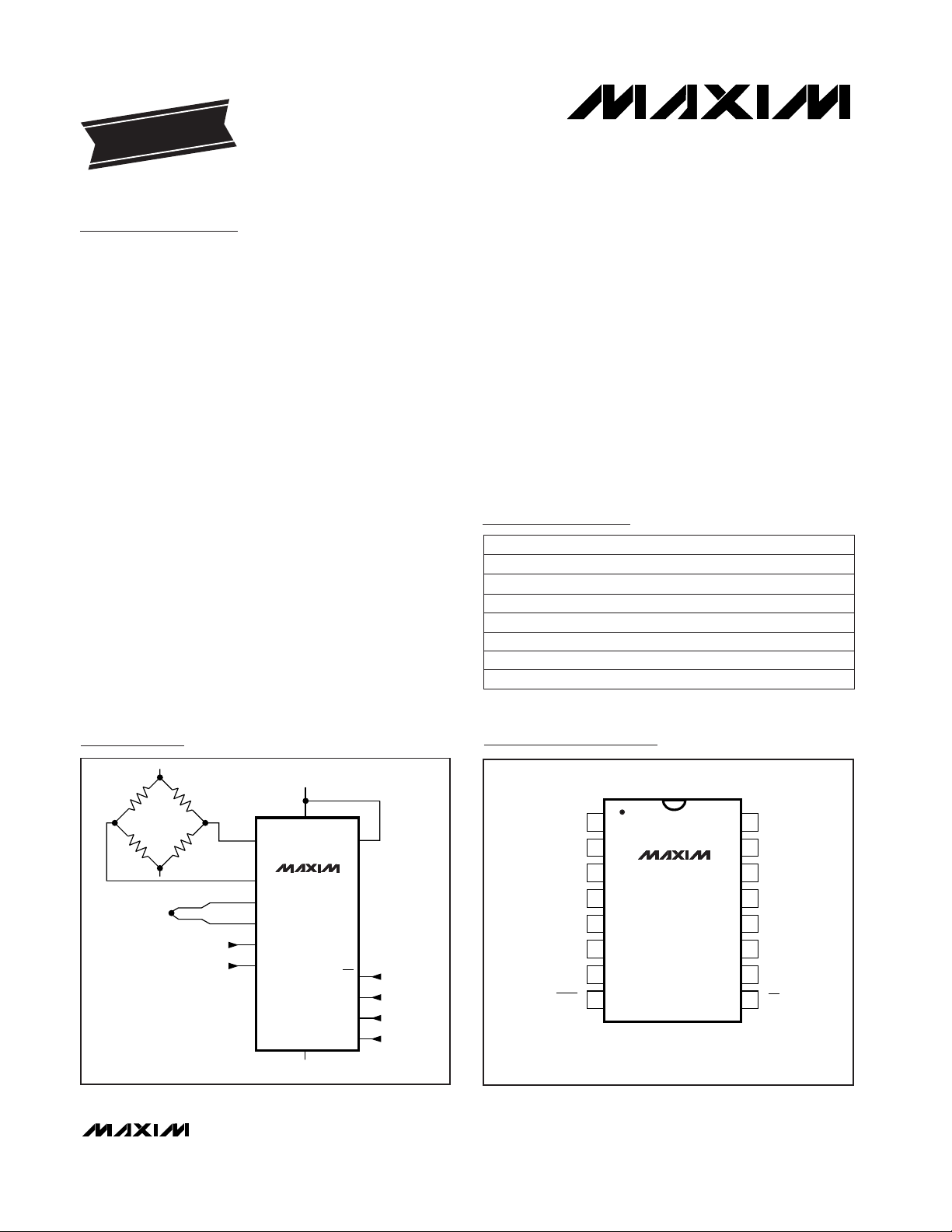
Typical Operating Circuit
Pin Configurations
IN1+
IN1-
REF+
REF-
CS
RCSEL
SCLK
DIN
DOUT
IN2+
IN2-
V
DD
+5V
-5V (0V)
FROM µC
MAX110
MAX111
( ) ARE FOR MAX111
V
SS
(AGND)
PART
MAX110ACPE
MAX110BCPE
MAX110ACWE 0°C to +70°C
0°C to +70°C
0°C to +70°C
TEMP. RANGE PIN-PACKAGE
16 Plastic DIP
16 Plastic DIP
16 Wide SO
MAX110BCWE 0°C to +70°C 16 Wide SO
MAX110ACAP 0°C to +70°C 20 SSOP
MAX110BCAP 0°C to +70°C 20 SSOP
EVALUATION KIT
AVAILABLE
MAX110BC/D 0°C to +70°C Dice*
Ordering Information continued at end of data sheet.
*
Contact factory for dice specifications.
SPI and QSPI are trademarks of Motorola, Inc. MICROWIRE is a trademark of National Semiconductor Corp.
Pin Configurations continued at end of data sheet.
INL(%)
±0.03
±0.05
±0.03
±0.05
±0.03
±0.05
±0.05
For free samples & the latest literature: http://www.maxim-ic.com, or phone 1-800-998-8800.
For small orders, phone 1-800-835-8769.
TOP VIEW
1
IN1+
REF-
2
REF+
3
4
V
DD
5
RCSEL
XCLK
6
7
SCLK
8
BUSY
( ) ARE FOR MAX111
MAX110
MAX111
DIP/SO
16
IN1-
15
IN2+
14
IN2-
13
V
GND
12
DIN
11
DOUT
10
CS
9
SS
(AGND)
Page 2
MAX110/MAX111
Low-Cost, 2-Channel, ±14-Bit Serial ADCs
2 _______________________________________________________________________________________
ABSOLUTE MAXIMUM RATINGS
VDDto GND ...........................................................................+6V
V
SS
to GND (MAX110)..............................................+0.3V to -6V
AGND to DGND.....................................................-0.3V to +0.3V
V
IN1+
, V
IN1-
......................................(VDD+ 0.3V) to (VSS- 0.3V)
V
IN2+
, V
IN2-
......................................(VDD+ 0.3V) to (VSS- 0.3V)
V
REF+
, V
REF-
....................................(VDD+ 0.3V) to (VSS- 0.3V)
Digital Inputs and Outputs .........................(V
DD
+ 0.3V) to -0.3V
Continuous Power Dissipation
16-Pin Plastic DIP (derate 10.53mW/°C above +70°C).....842mW
16-Pin Wide SO (derate 9.52mW/°C above +70°C) ......762mW
20-Pin SSOP (derate 8.00mW/°C above +70°C) ...........640mW
16-Pin CERDIP (derate 10.00mW/°C above +70°C)......800mW
Operating Temperature Ranges
MAX11_ _C_ _......................................................0°C to +70°C
MAX11_ _E_ _...................................................-40°C to +85°C
MAX11_BMJE.................................................-55°C to +125°C
Storage Temperature Range.............................-65°C to +160°C
Lead Temperature (soldering, 10sec).............................+300°C
Stresses beyond those listed under “Absolute Maximum Ratings” may cause permanent damage to the device. These are stress ratings only, and functional
operation of the device at these or any other conditions beyond those indicated in the operational sections of the specifications is not implied. Exposure to
absolute maximum rating conditions for extended periods may affect device reliability.
ELECTRICAL CHARACTERISTICS—MAX110
(VDD= 5V ±5%, VSS= -5V ±5%, f
XCLK
= 1MHz, ÷ 2 mode (DV2 = 1), 81,920 CLK cycles/conv, V
REF+
= 1.5V, V
REF-
= -1.5V,
TA= T
MIN
to T
MAX
, unless otherwise noted. Typical values are at TA= +25°C.)
LSB
nA500
CONDITIONS
I
IN+
, I
IN-
Input Bias Current
(Note 3) pF10
-0.83 x V
REF
≤ VIN≤ 0.83 x V
REF
-V
REF
≤ VIN≤ V
REF
-0.83 x V
REF
≤ VIN≤ 0.83 x V
REF
Input Capacitance
-V
REF
≤ VIN≤ V
REF
V
V
SS
+V
DD
-
2.25 2.25
V
IN+
,
V
IN-
Absolute Input Voltage
Range
V-V
REF
+V
REF
V
IN
Differential Input Voltage
Range
ppm
30
Power-Supply Rejection
15
ppm/°C8
Full-Scale Error
Temperature Drift
%
±0.1
µV/°C
0.003
Offset Error
Temperature Drift
(Note 6)
UNITSMIN TYP MAXSYMBOLPARAMETER
mV±4Offset Error
±0.018
±0.03 ±0.06
±0.015 ±0.03
±0.04
V
IN+
= V
IN-
= 0V
MAX110BC/E
MAX110AC/E
After gain calibration (Note 5)
After offset null
VSS= -5V, VDD= 4.75V to 5.25V
VDD= 5V, VSS= -4.75V to -5.25V
(Notes 3, 4) ±2DNLDifferential Nonlinearity
ppm/V6CMRR
Common-Mode Rejection
Ratio
-2.5V ≤ (V
IN+
= V
IN-
) ≤ 2.5V
Uncalibrated
-8 0
Full-Scale Error
Uncalibrated
0.02
-V
REF
≤ VIN≤ V
REF
-0.83 x V
REF
≤ VIN≤ 0.83 x V
REF
%FSRINL
Relative Accuracy
(Notes 3, 5–7)
±0.1
±0.05
MAX110BM
(Note 2)
14 + POL
+ OFL
RESResolution Bits
No-Missing-Codes
Resolution
(Note 3)
13 + POL
+ OFL
Bits
ACCURACY (Note 1)
ANALOG INPUTS
Page 3
MAX110/MAX111
Low-Cost, 2-Channel, ±14-Bit Serial ADCs
_______________________________________________________________________________________ 3
ELECTRICAL CHARACTERISTICS—MAX110 (continued)
(VDD= 5V ±5%, VSS= -5V ±5%, f
XCLK
= 1MHz, ÷ 2 mode (DV2 = 1), 81,920 CLK cycles/conv, V
REF+
= 1.5V, V
REF-
= -1.5V,
TA= T
MIN
to T
MAX
, unless otherwise noted. Typical values are at TA= +25°C.)
V
V4.75 5.25V
DD
Positive Supply Voltage
0.8V
IL
V-4.75 -5.25V
SS
Negative Supply Voltage
µA
Input Low Voltage
550 950
780
I
DD
Positive Supply Current
VDD= 5.25V,
VSS= -5.25V
320 650
Performance guaranteed by supply rejection test
Performance guaranteed by supply rejection test
pF10
0.4
VDD- 0.5
V
OH
Output High Voltage
Input Capacitance
f
XCLK
= 500kHz,
continuous-conversion mode
µA
µAI
SS
Negative Supply Current
VDD= 5.25V,
VSS= -5.25V
±1
20.48
410I
DD
I
LKG
Input Leakage Current
XCLK unloaded,
continuous-conversion mode, RC
oscillator operational (Note 9)
f
XCLK
= 500kHz,
continuous-conversion mode
(Note 3)
µA±10I
LKG
Leakage Current
pF10Output Capacitance
µA
0.05 2
Digital inputs at 0V or 5V
Power-Down Current
DOUT, BUSY, VDD= 4.75V, I
SOURCE
= 1.0mA
VDD= 5.25V, VSS= -5.25V, V
XCLK
= 0V, PD = 1
V
OUT
= 5V or 0V
(Note 3)
10,240 clock-cycles/conversion
DOUT, BUSY, I
SINK
= 1.6mA
CONDITIONS UNITSMIN TYP MAXSYMBOLPARAMETER
ms
204.80
t
CONV
Synchronous Conversion
Time (Note 7)
102,400 clock-cycles/conversion
MHz0.25 1.25f
OSC
Oversampling Clock
Frequency
(Note 8)
V2.4V
IH
Input High Voltage
I
SS
V0 3.0V
REF
Differential Reference
Input Voltage Range
pF10
Reference Input
Capacitance
(Note 3)
V
0.4
V
OL
Output Low Voltage
XCLK, I
SINK
= 200µA
V
VDD- 0.5
XCLK, VDD= 4.75V, I
SOURCE
= 200µA
nA500
I
REF+
,
I
REF-
Reference Input Current V
REF+
= 2.5V, V
REF-
= 0V
V
V
SS
+V
DD
-
2.25 2.25
V
REF+
,
V
REF-
Absolute Reference Input
Voltage Range
CONVERSION TIME
DIGITAL OUTPUTS (DOUT, BUSY, and XCLK when RCSEL = VDD)
POWER REQUIREMENTS (all digital inputs at 0V or 5V)
REFERENCE INPUTS
DIGITAL INPUTS (CS, SCLK, DIN, and XCLK when RCSEL = 0V)
Page 4
MAX110/MAX111
Low-Cost, 2-Channel, ±14-Bit Serial ADCs
4 _______________________________________________________________________________________
ELECTRICAL CHARACTERISTICS—MAX111
(VDD= 5V ±5%, f
XCLK
= 1MHz, ÷ 2 mode (DV2 = 1), 81,920 CLK cycles/conv, V
REF+
= 1.5V, V
REF-
= 0V, TA= T
MIN
to T
MAX
,
unless otherwise noted. Typical values are at TA= +25°C.)
LSB
nA500
CONDITIONS
I
IN+
, I
IN-
Input Bias Current
(Note 3) pF10
-0.667 x V
REF
≤ VIN≤ 0.667 x V
REF
-V
REF
≤ VIN≤ V
REF
-0.667 x V
REF
≤ VIN≤ 0.667 x V
REF
Input Capacitance
-V
REF
≤ VIN≤ V
REF
V0V
DD
- 3.2
V
IN+
,
V
IN-
Absolute Input Voltage
Range
V-V
REF
+V
REF
V
IN
Differential Input Voltage
Range
-V
REF
≤ VIN≤ V
REF
ppm15VDD= 4.75V to 5.25VPower-Supply Rejection
%FSRINL
ppm/°C8
Full-Scale Error
Temperature Drift
Relative Accuracy,
Differential Input
(Notes 3, 5–7)
(Notes 3, 4)
±0.25
±2
%
±0.2
±0.20
DNLDifferential Nonlinearity
(Note 6)
UNITSMIN TYP MAXSYMBOL
ppm/V6
(Note 2)
PARAMETER
14 + POL
+ OFL
RESResolution
CMRR
mV±4Offset Error
Common-Mode Rejection
Ratio
10mV ≤ (V
IN+
= V
IN-
) ≤ 2.0V
Bits
No-Missing-Codes
Resolution
±0.10
(Note 3)
-8 0
±0.05 ±0.10
Full-Scale Error
Uncalibrated
±0.03 ±0.05
MAX111BM
13 + POL
+ OFL
Bits
±0.18
V
IN+
= V
IN-
= 0V
MAX111BC/E
MAX111AC/E
After gain calibration (Note 5)
VIN≤ 0.667 x V
REF
0V ≤ VIN≤ V
REF
VIN≤ 0.667 x V
REF
0V ≤ VIN≤ V
REF
0V ≤ VIN≤ V
REF
VIN≤ 0.667 x V
REF
%FSRINL
Relative Accuracy,
Single-Ended Input
(IN- = GND)
±0.25
±0.15
±0.10
±0.1
±0.06
MAX111BM
±0.18
MAX111BC/E
MAX111AC/E
ACCURACY (Note 1)
ANALOG INPUTS
-0.667 x V
REF
≤ VIN≤ 0.667 x V
REF
Page 5
MAX110/MAX111
Low-Cost, 2-Channel, ±14-Bit Serial ADCs
_______________________________________________________________________________________ 5
ELECTRICAL CHARACTERISTICS—MAX111 (continued)
(VDD= 5V ±5%, f
XCLK
= 1MHz, ÷ 2 mode (DV2 = 1), 81,920 CLK cycles/conv, V
REF+
= 1.5V, V
REF-
= 0V, TA= T
MIN
to T
MAX
,
unless otherwise noted. Typical values are at TA= +25°C.)
V
V
V4.75 5.25V
DD
Positive Supply Voltage
0.4
ms
V
OL
0.8V
IL
204.80
Output Low Voltage
µA
Input Low Voltage
640 1200
t
CONV
Synchronous Conversion
Time (Note 7)
102,400 clock-cycles/conversion
XCLK, I
SINK
= 200µA
pF10
Reference Input
Capacitance
MHz0.25 1.25
nA
f
OSC
Oversampling Clock
Frequency
(Note 8)
V2.4V
IH
Input High Voltage
(Note 3)
V0 1.5V
REF
960
I
DD
Supply Current VDD= 5.25V
Differential Reference
Input Voltage Range
Performance guaranteed by supply rejection test
500
I
REF+
,
I
REF-
Reference Input Current
pF10
V
REF+
= 1.5V, V
REF-
= 0V
0.4
V0V
DD
- 3.2
V
REF+
,
V
REF-
VDD- 0.5
V
OH
Output High Voltage
Input Capacitance
Absolute Reference Input
Voltage Range
V
VDD- 0.5
f
XCLK
= 500kHz,
continuous-conversion mode
µA±1
XCLK, VDD= 4.75V, I
SOURCE
= 200µA
20.48
410
I
DD
I
LKG
Input Leakage Current
XCLK unloaded,
continuous-conversion mode, RC
oscillator operational (Note 9)
(Note 3)
µA±1I
LKG
Leakage Current
pF10Output Capacitance
µA
Digital inputs at 0V or 5V
Power-Down Current
DOUT, BUSY, VDD= 4.75V, I
SOURCE
= 1.0mA
VDD= 5.25V, V
XCLK
= 0V, PD = 1
V
OUT
= 5V or 0V
(Note 3)
10,240 clock-cycles/conversion
DOUT, BUSY, I
SINK
= 1.6mA
CONDITIONS UNITSMIN TYP MAXSYMBOLPARAMETER
CONVERSION TIME
DIGITAL OUTPUTS (DOUT, BUSY, and XCLK when RCSEL = VDD)
POWER REQUIREMENTS (all digital inputs at 0V or 5V)
REFERENCE INPUTS
DIGITAL INPUTS (CS, SCLK, DIN, and XCLK when RCSEL = 0V)
Page 6
MAX110/MAX111
Low-Cost, 2-Channel, ±14-Bit Serial ADCs
6 _______________________________________________________________________________________
Note 10: Timing specifications are guaranteed by design. All input control signals are specified with tr= tf= 5ns
(10% to 90% of +5V) and timed from a +1.6V voltage level.
Note 1: These specifications apply after auto-null and gain calibration. Performance at power-supply tolerance limits is guaranteed
by power-supply rejection tests. Tests are performed at V
DD
= 5V and VSS= -5V (MAX110).
Note 2: 32,768 LSBs cover an input voltage range of ±V
REF
(15 bits). An additional bit (OFL) is set for VIN> V
REF
.
Note 3: Guaranteed by design. Not subject to production testing.
Note 4: DNL is less than ±2 counts (LSBs) out of 2
15
counts (±14 bits). The major source of DNL is noise, and this can be further
improved by averaging.
Note 5: See
3-Step Calibration
section in text.
Note 6: V
REF
= (V
REF+
- V
REF-
), VIN= (V
IN1+
- V
IN1-
) or (V
IN2+
- V
IN2-
). The voltage is interpreted as negative when the voltage at
the negative input terminal exceeds the voltage at the positive input terminal.
Note 7: Conversion time is set by control bits CONV1–CONV4.
Note 8: Tested at clock frequency of 1MHz with the divide-by-2 mode (i.e. oversampling clock of 500kHz). See
Typical Operating
Characteristics
section for the effect of other clock frequencies. Also read the
Clock Frequency
section.
Note 9: This current depends strongly on C
XCLK
(see
Applications Information
section).
TIMING CHARACTERISTICS (see Figure 6)
(VDD= 5V, VSS= -5V (MAX110), TA= T
MIN
to T
MAX
, unless otherwise noted. Typical values are at TA= +25°C.)
MHz
1.1 3.0MAX11_ BM
RC Oscillator Frequency
1.3 2.8MAX11_ _C/E
2.0TA= +25°C
PARAMETER SYMBOL MIN TYP MAX UNITS
80
60
CS to SCLK Hold Time
(Note 10)
t
CSH
0 ns
DIN to SCLK Setup Time
(Note 10)
t
DS
100
ns
DIN to SCLK Hold Time
(Note 10)
t
DH
0 ns
100
60
80
CS to SCLK Setup Time
(Note 10)
t
CSS
100
ns
120
SCLK, XCLK Pulse Width
(Note 10)
t
CK
160
ns
03580
0 100
Data Access Time
(Note 10)
t
DA
0 120
ns
0 60 100
0 120
SCLK to DOUT Valid
Delay (Note 10)
t
DO
0 140
ns
35 80
Bus Relinquish Time
(Note 10)
t
DH
120
ns
MAX11_ BM
MAX11_ _C/E
TA= +25°C
MAX11_ BM
MAX11_ _C/E
CONDITIONS
MAX11_ _C/E
MAX11_ _C/E
MAX11_ BM
TA= +25°C
MAX11_ BM
TA= +25°C
C
LOAD
= 50pF
TA= +25°C
C
LOAD
= 50pF
MAX11_ _C/E
TA= +25°C
MAX11_ BM
TA= +25°C
MAX11_ _C/E/M
Page 7
MAX110/MAX111
Low-Cost, 2-Channel, ±14-Bit Serial ADCs
_______________________________________________________________________________________
7
-0.10
0
-0.05
0.05
0.10
-4 -2 0 2 4
MAX110 RELATIVE ACCURACY
(-V
REF
< VIN < V
REF
)
MAX110 toc01
VIN (V)
RELATIVE ACCURANCY (%FSR)
-40°C ≤ TA ≤ +85°C
RANGE OF INL VALUES
(200 PIECE SAMPLE SIZE)
-0.10
0
-0.05
0.05
0.10
-4 -2 0 2 4
MAX110 RELATIVE ACCURACY
(-0.83 V
REF
< V
IN
< 0.83 V
REF
)
MAX110 toc02
VIN (V)
RELATIVE ACCURANCY (%FSR)
-40°C ≤ TA ≤ +85°C
RANGE OF INL VALUES
(200 PIECE SAMPLE SIZE)
0.07
0.06
0.05
MAX110-TOC03
0.02
0.01
0
0 0.25 0.50 0.75 1.00 1.25
0.04
0.03
f
OSC
(MHz)
RELATIVE ACCURACY (%FSR)
÷1 MODE
÷2 MODE
÷ 4 MODE
VDD = 4.75V
V
SS
= -4.75V
T
A
= +85°C
MAX110 RELATIVE ACCURACY vs.
OVERSAMPLING FREQUENCY (f
OSC
)
0.10
MAX110-TOC04
0.04
0.02
0
-50
-25
0 25 50 75 100
0.08
0.06
TEMPERATURE (°C)
RELATIVE ACCURACY (%FSR)
MAX110 RELATIVE ACCURACY
vs. TEMPERATURE
8
6
7
MAX110-TOC05
3
2
0 0.25 0.50 0.75 1.00 1.25
4
5
f
OSC
(MHz)
POWER DISSIPATION (mW)
÷ 4 MODE
÷ 2 MODE
÷ 1 MODE
MAX110 POWER DISSIPATION vs.
OVERSAMPLING FREQUENCY (f
OSC
)
VDD = 5.25V
V
IN
= 0V
T
A
= -40°C
__________________________________________Typical Operating Characteristics
(MAX110, VDD= 5V, VSS= -5V, V
REF+
= 1.5V, V
REF-
= -1.5V, differential input (V
IN+
= -V
IN-
), f
XCLK
= 1MHz, ÷ 2 mode (DV2 = 1),
81,920 clocks/conv, TA = +25°C, unless otherwise noted.)
Page 8
MAX110/MAX111
Low-Cost, 2-Channel, ±14-Bit Serial ADCs
8 _______________________________________________________________________________________
____________________________Typical Operating Characteristics (continued)
(MAX111, VDD= 5V, V
REF+
= 1.5V, V
REF-
= 0V, differential input (V
IN+
= -V
IN-
), f
XCLK
= 1MHz, ÷ 2 mode (DV2 = 1),
81,920 clocks/conv, TA = +25°C, unless otherwise noted.)
0.14
0.12
0.1
MAX110-TOC08
0.04
0.02
0
0 0.25
0.50
0.75
1.00
0.08
0.06
f
OSC
(MHz)
RELATIVE ACCURACY (%FSR)
÷4 MODE
÷2 MODE
÷ 1 MODE
V
DD
= 4.75V
T
A
= +85°C
MAX111 RELATIVE ACCURACY vs.
OVERSAMPLING FREQUENCY (f
OSC
)
0.10
MAX110-TOC09
0.04
0.02
0
-50
-25
0 25 50 75 100
0.08
0.06
TEMPERATURE (°C)
RELATIVE ACCURACY (%FSR)
MAX111 RELATIVE ACCURACY
vs. TEMPERATURE
7
6
5
MAX110-TOC10
2
1
0
0 0.25 0.50 0.75 1.00 1.25
4
3
f
OSC
(MHz)
POWER DISSIPATION (mW)
÷ 4 MODE
÷ 2 MODE
÷ 1 MODE
MAX111 POWER DISSIPATION vs.
OVERSAMPLING FREQUENCY (f
OSC
)
VDD = 5.25V
V
IN
= 0V
T
A
= -40°C
0.10
0.05
0
-0.05
-0.10
MAX110-TOC6
V
IN
(V)
-2.0 -1.5 -1.0 -0.5 0 0.5 1.0 1.5 2.0
MAX111 RELATIVE ACCURACY
(-0.667V
REF
< VIN < 0.667V
REF
)
RELATIVE ACCURACY (%FSR)
0.10
0.05
0
-0.05
-0.10
MAX110-TOC7
V
IN
(V)
-2.0 -1.5 -1.0 -0.5 0 0.5 1.0 1.5 2.0
MAX111 RELATIVE ACCURACY
(-V
REF
< VIN < V
REF
)
RELATIVE ACCURACY (%FSR)
Page 9

MAX110/MAX111
Low-Cost, 2-Channel, ±14-Bit Serial ADCs
_______________________________________________________________________________________ 9
_______________Detailed Description
The MAX110/MAX111 ADC converts low-frequency
analog signals to a 16-bit serial digital output (14 data
bits, a sign bit, and an overrange bit) using a first-order
sigma-delta loop (Figure 1). The differential input voltage is internally connected to a precision voltage-tocurrent converter. The resulting current is integrated
and applied to a comparator. The comparator output
then drives an up/down counter and a 1-bit DAC. When
the DAC output is fed back to the integrator input, the
sigma-delta loop is completed.
During a conversion, the comparator output is a V
REF-
to V
REF+
square wave; its duty cycle is proportional to
the magnitude of the differential input voltage applied
to the ADC. The up/down counter clocks data in from
the comparator at the oversampling clock rate and
averages the pulse-width-modulated (PWM) square
wave to produce the conversion result. A 16-bit static
shift register stores the result at the end of the conversion. Figure 2 shows the ADC waveforms for a differential analog input equal to 1/2 (V
REF+
- V
REF-
). The
resulting comparator and 1-bit DAC outputs are high
for seven cycles and low for three cycles of the oversampling clock.
Since the analog input signal is integrated over many
clock cycles, much of the signal and quantization noise
is attenuated. The more clock cycles allowed during
each conversion, the greater the noise attenuation (see
Programming Conversion Time
).
______________________________________________________________Pin Description
Clock Input / RC Oscillator Output. TTL/CMOS-compatible oversampling clock input
when RCSEL = GND. Connects to the internal RC oscillator when RCSEL = V
DD
. XCLK
must be connected to V
DD
or GND through a resistor (1MΩ or less) when RC OSC
mode is selected.
XCLK8
Serial Clock Input. TTL/CMOS-compatible clock input for serial-interface data I/O.SCLK9
Busy Output. Goes low at conversion start, and returns high at end of conversion.
BUSY
10
Positive Power-Supply Input—connect to +5VV
DD
6
RC Select Input. Connect to GND to select external clock mode. Connect to VDDto
select RC OSC mode. XCLK must be connected to V
DD
or GND through a resistor
(1MΩ or less) when RC OSC mode is selected.
RCSEL7
Positive Reference InputREF+3
Negative Reference InputREF-2
Channel 1 Positive Analog InputIN1+1
FUNCTIONNAME
SSOP
6
7
8
4
5
3
2
PIN
1
DIP/SO
Chip-Select Input. Pull this input low to perform a control-word-write/data-read operation. A conversion begins when CS returns high, provided NO-OP is a 1. See the section
Using the MAX110/MAX111 with SPI, QSPI, and MICROWIRE Serial Interfaces.
CS
119
Serial Data Output. High-impedance when CS is high.
DOUT1210
Serial Data Input. See
Control Register
section.DIN1311
Digital GroundGND1612
MAX110 Negative Power-Supply Input—connect to -5VV
SS
Channel 2 Negative Analog InputIN2-1814
Channel 2 Positive Analog InputIN2+1915
Channel 1 Negative Analog InputIN1-2016
No Connect—there is no internal connection to this pinN.C.4, 5, 14, 15—
MAX111 Analog GroundAGND
1713
Page 10

MAX110/MAX111
Low-Cost, 2-Channel, ±14-Bit Serial ADCs
10 ______________________________________________________________________________________
Oversampling Clock
XCLK internally connects to a clock-frequency divider
network, whose output is the ADC oversampling clock,
f
OSC
. This allows the selected clock source (internal RC
oscillator or external clock applied to XCLK) to be
divided by one, two, or four (see
Clock Divider-Ratio
Control Bits
).
Figure 3 shows the two methods for providing the oversampling clock to the MAX110/MAX111. In externalclock mode (Figure 3a), the internal RC oscillator is
disabled and XCLK accepts a TTL/CMOS-level clock to
provide the oversampling clock to the ADC.
Select external-clock mode (Figure 3a) by connecting
RCSEL to GND and a TTL/CMOS-compatible clock to
XCLK (see
Selecting the Oversampling Clock
Frequency
).
In RC-oscillator mode (Figure 3b), the internal RC oscillator is active and its output is connected to XCLK
(Figure 1). Select RC-oscillator mode by connecting
RCSEL to VDD. This enables the internal oscillator and
connects it to XCLK for use by the ADC and external
system components. Minimize the capacitive loading on
XCLK when using the internal RC oscillator.
DIFFERENTIAL
ANALOG
INPUT
V
REF+
DC LEVEL AT 1/2 V
REF
V
REF-
V
REF+
V
REF-
OUTPUT FROM
1-BIT DAC
OVERSAMPLING
CLOCK
MAX110
MAX111
Figure 2. ADC Waveforms During a Conversion
Figure 1. Functional Diagram
IN1+
IN+
IN-
INPUT
MUX
IN1IN2+
IN2REF+
Gm
REF-
Gm
INTEGRATOR
UP/DOWN
COUNTER
-
Σ ∫
DITHER
GENERATOR
SERIAL
SHIFT
REGISTER
DIN SCLK CS
16 16
16 16
CONTROL
REGISTER
DOUT
BUSY
RCSEL
XCLK
OSC
TIMER + CONTROL
LOGIC + CLOCK GENERATOR
DIVIDER
NETWORK,
DIVIDE BY
1, 2, OR 4
RC
OSCILLATOR
MAX110
MAX111
Page 11

MAX110/MAX111
Low-Cost, 2-Channel, ±14-Bit Serial ADCs
______________________________________________________________________________________ 11
ADC Operation
The output data from the MAX110/MAX111 is arranged
in twos-complement format (Figures 4, 5). The sign bit
(POL) is shifted out first, followed by the overrange bit
(OR), and the 14 data bits (MSB first) (see Figure 6).
The MAX110 operates from ±5V power supplies and
converts low-frequency analog signals in the ±3V
range when using the maximum reference voltage of
V
REF
= 3V (V
REF
= V
REF+
- V
REF-
). Within the ±3V input
range, greater accuracy is obtained within ±2.5V (see
Electrical Characteristics
for details). Note that a nega-
tive input voltage is defined as V
IN-
> V
IN+
. For the
MAX110, the absolute voltage at any analog input pin
must remain within the (VSS+ 2.25V) to (VDD- 2.25V)
range.
The MAX111 operates from a single +5V supply and
converts low-frequency differential analog signals in the
±1.5V range when using the maximum reference voltage of V
REF
= 1.5V. As indicated in the
Electrical
Characteristics
, greater accuracy is achieved within the
±1.2V range. The absolute voltage at any analog input
pin for the MAX111 must remain within 0V to VDD- 3.2V.
When V
IN-
> V
IN+
the input is interpreted as negative.
The overrange bit (OFL) is provided to sense when the
input voltage level has exceeded the reference voltage
level. The converter does not “saturate” until the input
voltage is typically 20% larger. The linearity is not guaranteed in this range. Note that the overrange bit works
properly if the reference voltage remains within the recommended voltage range (see
Reference Inputs
). If the
reference voltage exceeds the recommended input
range, the overrange bit may not operate properly.
Digital Interface—Starting a Conversion
Data is transferred into and out of the serial I/O shift
register by pulling CS low and applying a serial clock
at SCLK. This fully static shift register allows SCLK to
range from DC to 2MHz. Output data from the ADC is
clocked out on SCLK’s falling edge and should be read
on SCLK’s rising edge. Input data to the ADC at DIN is
clocked in on SCLK’s rising edge. A new conversion
begins when CS returns high, provided the MSB in the
input control word (NO-OP) is a 1 (see
Using the
MAX110/MAX111 with MICROWIRE, SPI, and QSPI
Serial Interfaces
). Figure 6 shows the detailed serial-
interface timing diagram.
CCSS
must remain high during the conversion (while
BUSY remains low). Bringing CS low during the conver-
sion causes the ADC to stop converting, and may
result in erroneous output data.
Using the MAX110/MAX111 with SPI, QSPI, and
MICROWIRE Serial Interfaces
Figure 7 shows the most common serial-interface connections. The MAX110/MAX111 are compatible with
SPI, QSPI (CPHA = 0, CPOL = 0), and MICROWIRE
serial-interface standards.
XCLK
TTL/CMOS
RCSEL
GND
+5V
-5V (0V)
( ) ARE FOR MAX111.
V
DD
V
SS
(AGND)
MAX110
MAX111
Figure 3b. Connection for Internal RC-Oscillator Mode—XCLK
connects to the internal RC oscillator. Note, the pull-up resistor
is not necessary if the internal oscillator is never shut down.
XCLK
RCSEL
1MΩ
GND
+5V
-5V (0V)
V
DD
+5V
V
SS
(AGND)
MAX110
MAX111
( ) ARE FOR MAX111.
Figure 3a. Connection for External-Clock Mode
Page 12

MAX110/MAX111
Low-Cost, 2-Channel, ±14-Bit Serial ADCs
12 ______________________________________________________________________________________
OUTPUT
CODE
+OVERFLOW
TRANSITION
-OVERFLOW
TRANSITION
POL OFL D13...D0
0 1 00 . . .000
1 1 00 . . .001
1 1 00 . . .000
1 1 00 . . .010
1 0 11 . . .111
V
REF
-1LSB
INPUT VOLTAGE (LSBs)
- V
REF
0 0 11 . . .111
0 0 11 . . .110
0 0 11 . . .101
0 0 11 . . .100
+OVERFLOW
0 0 00 . . .001
0 0 00 . . .001
0 0 00 . . .000
1 1 11 . . .111
1 1 11 . . .110
1 1 00 . . .011
-OVERFLOW
Figure 4. Differential Transfer Function
OUTPUT
CODE
OVERFLOW
TRANSITION
POL OFL D13...D0
0 1 00 . . .000
0 0 00 . . .001
0 0 00 . . .000
0 0 00 . . .010
1 1 11 . . .111
V
REF
-1LSB
INPUT VOLTAGE (LSBs)
0123
0 0 11 . . .111
0 0 11 . . .110
0 0 11 . . .101
0 0 11 . . .100
+OVERFLOW
0 0 00 . . .011
Figure 5. Unipolar Transfer Function
Page 13

MAX110/MAX111
Low-Cost, 2-Channel, ±14-Bit Serial ADCs
______________________________________________________________________________________ 13
CS
SCLK
t
CSH
t
CSS
t
CK
t
DH
MSB LSB
t
DS
DIN
DOUT
BUSY
t
DH
t
CK
t
DO
t
DA
POL OFL MSB DO
END OF
CONVERSION
START OF
CONVERSION
Figure 6. Detailed Serial-Interface Timing
The ADC serial interface operates with just SCLK, DIN,
and DOUT (allow sufficient time for the conversion to
complete between read/write operations). Achieve continuous operation by connecting BUSY to an uncommitted µP I/O or interrupt, to signal the processor when the
conversion results are ready. Figures 8a and 8b show
the timing for SPI/MICROWIRE and QSPI operation.
The fully static 16-bit I/O register allows infinite time
between the two 8-bit read/write operations necessary
to obtain the full 16 bits of data with SPI and
MICROWIRE. CS must remain low during the entire
two-byte transfer (Figure 8a). QSPI allows a full 16-bit
data transfer (Figure 8b).
Interfacing to the 80C32 Microcontroller Family
Figure 7c shows the general 80C32 connection to the
MAX110/MAX111 using Port 1. For a more detailed discussion, see the MAX110 evaluation kit manual.
I/O Shift Register
Serial data transfer is accomplished with a 16-bit fully
static shift register. The 16-bit control word shifted into
this register during a data-transfer operation controls
the ADC’s various functions. The MSB (NO-OP)
enables/disables transfer of the control word within the
ADC. A logic 1 causes the remaining 15 bits in the control word to be transferred from the I/O register into the
control register when CS goes high, updating the
ADC’s configuration and starting a new conversion. If
I/O
SCK
MISO
MOSI
MASKABLE
INTERRUPT
SS
a. SPI/QSPI
+5V
µP
CS
SCLK
DOUT
DIN
BUSY
MAX110
MAX111
I/O
SK
SI
SO
MASKABLE
INTERRUPT or I/O
b. MICROWIRE
µP
CS
SCLK
DOUT
DIN
BUSY
P1.0
P1.1
P1.2
P1.3
P1.4
c. 80C51/80C32
µP
CS
SCLK
DIN
DOUT
BUSY
MAX110
MAX111
MAX110
MAX111
Figure 7. Common Serial-Interface Connections
Page 14

MAX110/MAX111
Low-Cost, 2-Channel, ±14-Bit Serial ADCs
14 ______________________________________________________________________________________
BUSY
1
ST
BYTE READ/WRITE 2ND BYTE READ/WRITE
CS
SCLK
DOUT
POL OFL D13 D12 D11 D10 D9 D8 D7 D6 D5 D4 D3 D2 D1 D0
NO OP
NU NU
CONV4 CONV3 CONV2 CONV1
DV4 DV2 NU NU CHS CAL NUL PDX PD
DIN
MAX110
MAX111
Figure 8a. SPI/MICROWIRE-Interface Timing
BUSY
CS
SCLK
DOUT
POL OFL D13 D12 D11 D10 D9 D8 D7 D6 D5 D4 D3 D2 D1 D0
NO OP NU NU
CONV4 CONV3 CONV2 CONV1
DV4 DV2 NU NU CHS CAL NUL PDX PD
DIN
MAX110
MAX111
Figure 8b. QSPI Serial-Interface Timing
Page 15

MAX110/MAX111
Low-Cost, 2-Channel, ±14-Bit Serial ADCs
______________________________________________________________________________________ 15
NO-OP is a zero, the control word is not transferred to
the control register, the ADC’s configuration remains
unchanged, and no new conversion is initiated. This
allows specific ADCs in a “daisy chain” arrangement to
be reconfigured while leaving the remaining ADCs
unchanged. Table 1 lists the various ADC control word
functions.
Output data is shifted out of DOUT at the same time the
input control word for the next conversion is shifted in
(Figure 8).
On power-up, all internal registers reset to zero.
Therefore, when writing the first control word to the
ADC, the data simultaneously shifted out will be zeros.
The first conversion begins when CS goes high (NO-OP
= 1). The results are placed in the 16-bit I/O register for
access on the next data-transfer operation.
Power-Down Mode
Bits 0 and 1 control the ADC’s power-down mode. If bit
0 (PD) is a logic high, power is removed from all analog
circuitry except the RC oscillator. A logic high at bit 1
(PDX) removes power from the RC oscillator. If both bits
PD and PDX are a logic high, or if PD is high and
RCSEL is low, the supply currents reduce to 4µA. If an
external XCLK clock continues to run in power-down
mode, the supply current will depend on the clock rate.
When PDX is set high, the internal RC oscillator stops
shortly after CS returns high. If the next control word
written to the device has NO-OP = 1 instructing the
ADC to convert, BUSY will go low, but because the RC
oscillator is stopped, BUSY will remain low and will not
allow a new conversion to begin. To avoid this situation,
write a “dummy” control word with NO-OP = 0 and any
combination of bits 14-0 in the control word following
the control word with PDX = 0. With NO-OP = 0, bits 140 are ignored and the internal state machine resets.
Next, perform a normal 3-step calibration (see Table 3).
Note that XCLK must be connected to V
DD
or GND
through a resistor (suggested value is 1MΩ) when the
RC oscillator mode is selected (RCSEL = VDD). This
resistor is not necessary if the external oscillator mode
is used, or if the internal oscillator is not shut down.
Selecting the Analog Inputs
Bit 4 (CHS) controls which of the two differential inputs
connect to the internal ADC inputs (see the
Functional
Diagram
). A logic high selects IN2+ and IN2- while a
logic low selects IN1+ and IN1-. Table 2 shows the
allowable input multiplexer configurations.
Table 1. Input Control-Word Bit Map
↑
First bit clocked in.
PD
PDXNULCALCHSNUNUDV2DV4CONV1CONV2CONV3CONV4NUNU
NO-OP
0123456789101112131415
Analog Power-Down. Set this bit high to power down the analog section.PD0
Oscillator Power-Down. Set this bit high to power down the RC oscillator.PDX1
Internal Offset-Null Bit. A logic high selects offset-null mode. See Table 3.NUL2
Gain-Calibration Bit. A logic high selects gain-calibration mode. See Table 3.CAL3
Input Channel Select. A logic high selects channel 2 (IN2+ and IN2-), while a logic low
selects channel 1 (IN1+ and IN1-). See Tables 2 and 3.
CHS4
XCLK to Oversampling Cock Ratio Control Bits. See Table 5.DV2, DV47, 8
Conversion Time Control Bits. See Table 4.CONV1–CONV49–12
Used for test purposes only. Set these bits low.NU5, 6, 13, 14
If this bit is a logic high, the remaining 15 LSBs are transferred to the control register and a
new conversion begins when CS returns high. If this bit is set low, the control word is not
passed to the control register, the ADC configuration remains unchanged, and no new conversion begins when CS returns high.
NO-OP
15
DESCRIPTIONNAMEBIT
Page 16

MAX110/MAX111
Low-Cost, 2-Channel, ±14-Bit Serial ADCs
16 ______________________________________________________________________________________
X = Don't Care
Table 3. Procedure to Calibrate the ADC
0010
0
or
1
00XX
No
Change
001
Performs an offset-null conversion with the
internal ADC inputs shorted to the selected
input channel's negative input (IN1- or IN2-).
The next operation performs the first signal
conversion with the new setup.
3
0001X00XX
No
Change
001
Performs a gain-calibration conversion with
the null register contents as the starting value.
The result is stored in the calibration register.
2
0011X00XX
New
Data
001
Sets the new conversion speed (if required)
and performs an offset correction conversion
with the internal ADC inputs shorted to REF-.
The result is stored in the null register.
(This step also selects the speed/resolution
for the ADC.)
1
PD
PDXNULCALCHS
Not
Used
DV2 &
DV4
CONV1-
CONV4
Not
Used
NNOO--OOPP
DESCRIPTIONSTEP
CONTROL WORD
X = Don't Care
Table 2. Allowable Input Multiplexer Configurations
Input control word is not transferred to the control register. ADC
configuration remains unchanged and no new conversion starts when CS
returns high.
No
Change
No
Change
0XXX
REF+ and REF- connected to the ADC inputs; gain-calibration mode
selected. Autocal conversion begins when CS returns high, and the results are
stored in the 16-bit I/O register.
REF-REF+1X01
REF- connected to the ADC inputs; offset-null mode selected. Autonull conversion
begins when CS returns high, and the results are stored in the null register.
REF-REF-1X11
IN2- connected to the ADC inputs; offset-null mode selected. Autonull conversion
begins when CS returns high, and the results are stored in the null register.
IN2-IN2-1110
IN1- connected to the ADC inputs; offset-null mode selected. Autonull conversion
begins when CS returns high, and the results are stored in the null register.
IN1-IN1-1010
Channel 2 connected to ADC inputs. Conversion begins when CS returns high.
IN2-IN2+1100
Channel 1 connected to ADC inputs. Conversion begins when CS returns high.
IN1-IN1+1000
DESCRIPTIONADC IN-ADC IN+
NNOO--OOPP
CHSNULCAL
Page 17

MAX110/MAX111
Low-Cost, 2-Channel, ±14-Bit Serial ADCs
______________________________________________________________________________________ 17
3-Step Calibration
The data sheet electrical specifications apply to the
device after optional calibration of gain error and offset.
Uncalibrated, the gain error is typically 2%.
Table 3 describes the three steps required to calibrate
the ADC completely.
Once the ADC is calibrated to the selected channel, set
CAL = 0 and NUL = 0 and leave CHS unchanged in the
next control word to perform a signal conversion on the
selected analog input channel.
Calibrate the ADC after the following operations:
— when power is first applied
— if the reference common-mode voltage changes
— if the common-mode voltage of the selected input
channel varies significantly. The CMRR of the analog
inputs is 0.25LSB/V.
— after changing channels (if the common-mode volt-
ages of the two channels are different)
— after changing conversion speed/resolution.
— after significant changes in temperature. The offset
drift with temperature is typically 0.003µV/°C.
Automatic gain calibration is not allowed in the
102,400 cycles per conversion mode (see
Programming Conversion Time
). In this mode, calibration can be achieved by connecting the reference voltage to one input channel and performing a normal
conversion. Subsequent conversion results can be corrected by software. Do not issue a
NNOO--OOPP
command
directly following the gain calibration, as the calibration data will be lost.
Programming Conversion Time
The MAX110/MAX111 are specified for 12 bits of accuracy and up to ±14 bits of resolution. The ADC’s resolution depends on the number of clock cycles allowed
during each conversion. Control-register bits 9–12
(CONV1–CONV4) determine the conversion time by
controlling the nominal number of oversampling clock
cycles required for each conversion (OSCC/CONV).
Table 4 lists the available conversion times and resulting resolutions.
To program a new conversion time, perform a 3-step
calibration with the appropriate CONV1–CONV4 data
used in Table 3. The ADC is now calibrated at the new
conversion speed/resolution.
Table 4. Available Conversion Times
* Gain-calibration mode is not available with 102,400 clock cycles/conversion selected.
Clock duty cycles of 50% ±10% are recommended.
Table 5. Clock Divider-Ratio Control
CONV4 CONV3 CONV2 CONV1
CLOCK CYCLES
PER
CONVERSION
NOMINAL CONVERSION TIME
RCSEL = GND, DV2 = DV4 = 0, XCLK = 500kHz
(ms)
CONVERSION
RESOLUTION
(Bits)
1 0 0 1 10,240 20.48 12 + POL
0 0 1 1 20,480 40.96 13 + POL
0 1 1 0 81,920 163.84 14 + POL
0 0 0 0 102,400* 204.80 14 + POL
Not allowed11
XCLK or internal RC oscillator is divided by 2 and connects to the ADC; f
OSC
= f
XCLK
÷ 2.
01
XCLK or internal RC oscillator is divided by 4 and connects to the ADC; f
OSC
= f
XCLK
÷ 4.
10
XCLK or internal RC oscillator connects directly to the ADC; f
OSC
= f
XCLK
.00
DESCRIPTIONDV4DV2
Page 18

MAX110/MAX111
Low-Cost, 2-Channel, ±14-Bit Serial ADCs
18 ______________________________________________________________________________________
Selecting the Oversampling
Clock Frequency
Choose the oversampling frequency, f
OSC
, carefully to
achieve the best relative-accuracy performance from the
MAX110/MAX111 (see
Typical Operating Characteristics
).
Clock Divider-Ratio Control Bits
Bits 7 and 8 (DV2 and DV4) program the clockfrequency divider network. The divider network sets the
frequency ratio between f
XCLK
(the frequency of the
external TTL/CMOS clock or internal RC oscillator) and
f
OSC
(the oversampling frequency used by the ADC).
An oversampling clock frequency between 450kHz and
700kHz is optimum for the converter. Best perfor-
mance over the extended temperature range is
obtained by choosing 1MHz or 1.024MHz with the
divide-by-2 option (DV2 = 1) (see the section
Effect
of Dither on INL
). To determine the converter’s accura-
cy at other clock frequencies, see the
Typical
Operating Characteristics
and Table 5.
Effect of Dither on Relative Accuracy
First-order sigma-delta converters require dither for
randomizing any systematic tone being generated in
the modulator. The frequency of the dither source plays
an important role in linearizing the modulator. The ratio
of the dither generator’s frequency to that of the modulator’s oversampling clock can be changed by setting
the DV2/DV4 bits. The XCLK clock is directly used by
the dither generator while the DV2/DV4 bits reduce the
oversampling clock by a ratio of 2 or 4. Over the commercial temperature range, any ratio (i.e., 1, 2, or 4)
between the dither frequency and the oversampling
clock frequency can be used for best performance.
Over the extended and military temperature ranges, the
ratio of 2 or 4 gives the best performance. See the
Typical Operating Characteristics
to observe the effect
of the clock divider on the converter’s linearity.
50Hz/60Hz Line Frequency Rejection
High rejection of 50Hz or 60Hz is obtained by using an
oversampling clock frequency and a clock-cycles/conversion setting so the conversion time equals an integral number of line cycles, as in the following equation:
f
OSC
= f
LINE
x m / n
where f
OSC
is the oversampling clock frequency, f
LINE
= 50Hz or 60Hz, m is the number of clock cycles per
conversion (see Table 4), and n is the number of line
cycles averaged every conversion.
This noise rejection is inherent in integrating and
sigma-delta ADCs, and follows a SIN(X) / X function
(Figure 9). Notches in this function represent extremely
high rejection, and correspond to frequencies with an
integral number of cycles in the MAX110/MAX111’s
selected conversion time.
The shortest conversion time resulting in maximum
simultaneous rejection of both 60Hz and 50Hz line frequencies is 100ms. When using the MAX111, use a
200ms conversion time for maximum 60Hz and 50Hz
rejection and optimum performance. For either device,
select the appropriate oversampling clock frequency
and either an 81,240 or 102,400 clock cycles per conversion (CCPC) ratio. Table 6 suggests the possible
configurations.
0
-10
-20
-30
-40
-50
-60
0.1
1
CONVERSION TIME
LINE CYCLE PERIOD
SIGNAL FREQUENCY IN Hz
FOR 100ms CONVERSION
TIME (see Table 6)
1
10 20 30 40 50 60 708090100
2345678910
GAIN (dB)
Figure 9. MAX110/MAX111 Noise Rejection Follows SIN(X) / X Function
Page 19

MAX110/MAX111
Low-Cost, 2-Channel, ±14-Bit Serial ADCs
______________________________________________________________________________________ 19
A 100ms conversion time cannot be achieved with either
10,240 CCPC or 20,480 CCPC modes because f
OSC
would be below the minimum 250kHz requirement.
When the gain calibration is performed, the conversion
times change approximately 1% to compensate for the
modulator’s gain error. This slightly degrades the linefrequency rejection, because the corrected conversion
time is no longer an exact multiple of the line frequency.
Typically, the rejection of 50Hz/60Hz from the converter
is 55dB; i.e., if there is 100mV injection at the reference
or the analog input pin, it will cause an uncertainty of
±0.006%. If the system has large 50Hz/60Hz noise, the
use of internal auto gain calibration is not recommended. Instead, gain calibration should be done off-chip,
using numerical computation methods.
If you wish to use a configuration other than those suggested in Table 6, you can accomplish similar 50Hz
and 60Hz line-frequency rejection off-chip by averaging several conversions.
__________Applications Information
Layout, Grounding, Bypassing
For minimal noise, bypass each supply to GND with a
0.1µF capacitor. A ground plane should also be placed
under the analog circuitry. To minimize the coupling
effects of stray capacitance, keep digital lines as far
from analog components and lines as possible. Figure
10 shows the suggested power-supply and groundplane connections.
*R = 10Ω
*OPTIONAL
DIGITAL
CIRCUITRY
POWER
SUPPLIES
V
DD
V
SS
+5V DGND
+5V -5V GND
GND
4.7µF
0.1µF
0.1µF
4.7µF
MAX110
Figure 10a. MAX110 Power-Supply Grounding Connections
*R = 10Ω
*OPTIONAL
DIGITAL
CIRCUITRY
POWER
SUPPLIES
V
DD
AGND +5V DGND
+5V
GND
GND
4.7µF
0.1µF
MAX111
Figure 10b. MAX111 Power-Supply Grounding Connections
CCPC = Clock Cycles per Conversion
Table 6. Suggested XCLK Frequencies to Achieve Maximum Rejection of Both 50Hz/60Hz Line
Frequencies
MAX111 (t
CONVERT
= 200ms)
81,240 CCPC 102,400 CCPC
DIVIDER
RATIO
f
XCLK
(MHz)
RELATIVE
ACCURACY
(%)
f
XCLK
(MHz)
RELATIVE
ACCURACY
(%)
1:1 0.4062 0.030 0.512 0.030
2:1 0.8124 0.025 1.024 0.025
4:1 1.6248 0.022 2.048 0.023
MAX110 (t
CONVERT
= 100ms)
81,240 CCPC 102,400 CCPC
DIVIDER
RATIO
f
XCLK
(MHz)
RELATIVE
ACCURACY
(%)
f
XCLK
(MHz)
RELATIVE
ACCURACY
(%)
1:1 0.8124 0.025 1.024 0.065
2:1 1.6248 0.018 2.048 0.045
4:1 3.2496 0.016 4.096 0.030
Page 20

MAX110/MAX111
Low-Cost, 2-Channel, ±14-Bit Serial ADCs
20 ______________________________________________________________________________________
Capacitive Loading Effects of XCLK in
Internal RC-Oscillator Mode
When using the internal RC oscillator, capacitive loading effects on the XCLK pin must be minimized. Stray
capacitance causes the VDDpower consumption to
increase by an amount p = 1⁄2CV2f, where C = stray
capacitance, V is the supply voltage, and f is the frequency of the internal RC oscillator.
External Reference
The reference inputs to the ADC are high impedance,
allowing both an external voltage reference and ratiometric applications without loading effects. The fully differential analog signal and reference inputs are
advantageous for performing ratiometric conversions
(Figures 11 and 12). For example, when measuring
load cells, the bridge excitation and the ADC reference
input both share the same voltage source. As the excitation changes with temperature or voltage, the output
of the load cell will change. But since the differential
reference voltage also changes, the conversion results
remain constant, all else remaining equal.
Weigh Scale Application
The fully differential analog signal and reference inputs
make the MAX111 easy to interface to transducers with
differential outputs, such as the load cell in Figure 11.
Because the ADC input is differential, the load cell only
requires differential gain, eliminating the need for the
difference amplifier (differential to single-ended converter) of the standard three op-amp instrumentationamplifier realization.
The 30mV full-scale bridge output is amplified to 2V
full-scale and applied to the MAX111 channel-one
input. The reference voltage to the ADC is created by a
voltage divider connected to the +5V rail. The same 5V
provides excitation for the bridge; therefore, as the
excitation voltage varies, the reference voltage to the
ADC also varies, providing an ADC output that does
not depend on the supply voltage.
The two 121kΩ resistors connected to the +5V supplies
shift the common-mode voltage from 2.5V (5V/2) to
1.5V to ensure linearity. Match these two resistors to
avoid introducing differential offset, or trim the resistor
mismatch with a potentiometer. In practice, the scale is
“zeroed” or “tared” by storing the average of several
conversions in a memory location while the scale is
+5V
30mV
FULL-SCALE
121k
2k
121k
49.9k
1k
22k
10k
1k
1k
1/2 MAX492
1/2 MAX492
1µF
1µF
REF+
REF-
IN1+
IN1-
AGND
CS
DIN
DOUT
SCLK
49.9k
V
DD
+5V
0.1µF
MAX111
+5V
+5V
+5V
GND
Figure 11. Weigh Scale Application
Page 21

unloaded, and subtracting this value from actual weight
measurements. The lowpass filtering action of the
MAX111’s sigma-delta converter helps minimize noise.
The resolution of the weigh scale can be further
increased by averaging several conversions.
Thermocouple Circuit with Software
Compensation
A thermocouple is created by the junction of dissimilar
metals, and generates a voltage proportional to temperature (Seebeck voltage), making it useful for temperature-measurement instruments. When a thermocouple
probe is connected to a measurement instrument, other
thermoelectric potentials are created between the alloys
of the probe and the copper connectors of the instrument. These potentials introduce a temperature-dependent error that must be subtracted from the temperature
measurement to obtain an accurate result. According to
the law of intermediate metals, the junction of the thermocouple-probe alloys with the copper of the instrument
junction block can be treated as another thermocouple
of the same type. The voltage measured by the instrument can be expressed as:
V = α(T1 - T
REF
)
where α is the Seebeck constant for the type of thermocouple, T1 is the temperature being measured, and
T
REF
is the temperature of the junction block. Although
one method to obtain T
REF
is to force the junction block
to a known temperature (0°C), a more popular
approach is to measure T
REF
directly using a thermistor
or PN junction voltage.
The circuit in Figure 12 shows a k-type thermocouple
going through a 54dB gain stage to channel 1 of the
MAX110. A MAX874 voltage reference provides both
the 3V reference voltage and reference junction temperature information to the MAX110. Armed with the
temperature information provided by the MAX874, the
thermocouple voltage created at the junction block can
be subtracted out in software. The TEMP output of the
MAX874 is nominally 690mV at room temperature, and
increases with temperature at about 2.3mV/°C. Place
the MAX874 as close as possible to the terminal block,
and ensure good thermal contact between them. This
circuit employs a common k-type thermocouple and,
with the component values shown, can indicate temperatures in the range of -150°C to +125°C.
MAX110/MAX111
Low-Cost, 2-Channel, ±14-Bit Serial ADCs
______________________________________________________________________________________ 21
243k
1k
1k
10k
1µF
1µF
IN1+
IN1-
REF-
REF+
V
SS
-5V
CS
DIN
DOUT
SCLK
243k
1M
1k
10k 10k
K-TYPE
V
DD
+5V
IN2-
IN2+
MAX110
1/4 MAX479
1/4 MAX479
1/4 MAX479
TEMP
OUT
V
IN
MAX874
+5V
Figure 12. Thermocouple Circuit with Software Compensation
Page 22

MAX110/MAX111
Low-Cost, 2-Channel, ±14-Bit Serial ADCs
22 ______________________________________________________________________________________
TOP VIEW
1
2
3
4
5
6
7
8
20
19
18
17
16
15
14
13
IN1+
REFREF+
N.C.
N.C.
V
DD
RCSEL
XCLK
IN1IN2+
IN2V
SS
(AGND)
GND
N.C.
N.C.
DIN
9
10
12
11
SCLK
BUSY
DOUT
CS
MAX110
MAX111
SSOP
( ) ARE FOR MAX111
____Pin Configurations (continued)
_Ordering Information (continued)
__________________Chip Topography
TRANSISTOR COUNT: 5849
SUBSTRATE CONNECTED TO V
DD
V
SS
(AGND)
RCSEL
REF+
DOUT
XCLK
0.168"
(4.27mm)
0.121"
(3.07mm)
SCLK BUSY CS DIN
V
SS
(AGND)
GND
GND
REF-IN1+ IN1- IN2+ IN2-
V
DD
V
DD
( ) ARE FOR MAX111
±0.0516 Plastic DIP-40°C to +85°CMAX110BEPE
±0.05
±0.05
±0.03
±0.05
±0.03
±0.03
INL(%)
16 CERDIP**-55°C to +125°CMAX110BMJE
20 SSOP-40°C to +85°CMAX110BEAP
20 SSOP-40°C to +85°CMAX110AEAP
16 Wide SO
16 Wide SO
16 Plastic DIP
PIN-PACKAGETEMP. RANGE
-40°C to +85°C
-40°C to +85°C
-40°C to +85°CMAX110BEWE
MAX110AEWE
MAX110AEPE
PART
MAX111ACPE
0°C to +70°C 16 Plastic DIP ±0.03
MAX111BCPE 0°C to +70°C 16 Plastic DIP ±0.05
MAX111ACWE 0°C to +70°C 16 Wide SO ±0.03
MAX111BCWE 0°C to +70°C 16 Wide SO ±0.05
MAX111ACAP 0°C to +70°C 20 SSOP ±0.03
MAX111BCAP 0°C to +70°C 20 SSOP ±0.05
MAX111BC/D 0°C to +70°C Dice* ±0.05
MAX111AEPE -40°C to +85°C 16 Plastic DIP ±0.03
MAX111BEPE -40°C to +85°C 16 Plastic DIP ±0.05
MAX111AEWE -40°C to +85°C 16 Wide SO ±0.03
MAX111BEWE -40°C to +85°C 16 Wide SO ±0.05
MAX111AEAP -40°C to +85°C 20 SSOP ±0.03
MAX111BEAP -40°C to +85°C 20 SSOP ±0.05
MAX111BMJE -55°C to +125°C 16 CERDIP** ±0.05
*
Contact factory for dice specifications.
**
Contact factory for availability.
Page 23

MAX110/MAX111
Low-Cost, 2-Channel, ±14-Bit Serial ADCs
______________________________________________________________________________________ 23
_______________________________________________________Package Information
PDIPN.EPS
SOICW.EPS
Page 24

MAX110/MAX111
Low-Cost, 2-Channel, ±14-Bit Serial ADCs
___________________________________________Package Information (continued)
CDIPS.EPS
Maxim cannot assume responsibility for use of any circuitry other than circuitry entirely embodied in a Maxim product. No circuit patent licenses are
implied. Maxim reserves the right to change the circuitry and specifications without notice at any time.
24
____________________Maxim Integrated Products, 120 San Gabriel Drive, Sunnyvale, CA 94086 408-737-7600
© 1998 Maxim Integrated Products Printed USA is a registered trademark of Maxim Integrated Products.
SSOP.EPS
 Loading...