

Page 1
General Description
The MAX11043 features 4 single-ended or differential
channels of simultaneous-sampling ADCs with 16-bit
resolution. The MAX11043 contains a versatile filter
block and programmable-gain amplifier (PGA) per
channel. The filter consists of seven cascaded 2ndorder filter sections for each channel, allowing the construction of a 14th-order filter. The filter coefficients are
user-programmable. Configure each 2nd-order filter as
lowpass (LP), highpass (HP), or bandpass (BP) with
optional rectification. Gain and phase mismatch of the
analog signal path is better than -50dB.
The ADC can sample up to 800ksps per channel. A
40MHz serial interface provides communication to and
from the device. The SPI™ interface provides throughput of 1600ksps; 4 channels at 400ksps per channel or
2 channels at 800ksps per channel. A software-selectable scan mode allows reading the ADC results while
simultaneously updating the DAC. Other features of the
MAX11043 include an internal (+2.5V) or external
(+2.0V to +2.8V) reference, power-saving modes, and
a PGA with gains of 1 to 64. The PGA includes an
equalizer (EQ) function that automatically boosts lowamplitude, high-frequency signals for applications such
as CW-chirp radar.
The MAX11043 includes two 8-bit coarse DACs that set
the high and low references for a second-stage 12-bit
fine DAC, typically used for VCO control. Use software
controls to write to the DAC or step the DAC up and
down under hardware control in programmable steps.
The device operates from a +3.0V to +3.6V supply. The
MAX11043 is available in a 40-pin, 6mm x 6mm TQFN
package and operates over the extended -40°C to
+125°C temperature range.
Applications
Automotive Radar Systems
Data Acquisition Systems
Industrial Controls
Power-Grid Monitoring
Features
♦ 4 Single-Ended or Differential Channels of
Simultaneous-Sampling, 16-Bit ADCs
♦ ±10 LSB INL, ±1 LSB DNL, No Missing Codes
♦ 90dB SFDR, -86dB THD, 76dB SINAD,
77dB SNR at 100kHz Input
♦ PGA with Gain of 1, 2, 4, 8, 16, 32, or 64 for
Each Channel
♦ EQ Function Automatically Boosts
High-Frequency, Low-Amplitude Signals
♦ Seven-Stage Internal Programmable Biquad
Filters per Channel
♦ High Throughput, 400ksps per Channel for 4
Channels or 800ksps per Channel for 2 Channels
♦ Dual-Stage DAC
Two 8-Bit Coarse Reference DACs
12-Bit Fine DAC
♦ +2.5V Internal Reference or +2.0V to +2.8V
External Reference
♦ Single +3.3V Operation
♦ Shutdown and Power-Saving Modes
♦ 40-Pin, 6mm x 6mm TQFN Package
♦ -40°C to +125°C Operating Temperature
MAX11043
4-Channel, 16-Bit, Simultaneous-Sampling ADCs
with PGA, Filter, and 8-/12-Bit Dual-Stage DAC
________________________________________________________________
Maxim Integrated Products
1
Pin Configuration
Ordering Information
19-4250; Rev 0; 8/08
For pricing, delivery, and ordering information, please contact Maxim Direct at 1-888-629-4642,
or visit Maxim’s website at www.maxim-ic.com.
PART TEMP RANGE PIN-PACKAGE
MAX11043ATL+
40 TQFN-EP*
+
Denotes a lead-free/RoHS-compliant package.
*
EP = Exposed pad.
SPI is a trademark of Motorola, Inc.
-40°C to +125°C
TOP VIEW
REFDACL
AOUT
AVDD
25
AGND
DGND
*EP
8910
DVDD
21
SHDN
20
19
18
17
16
15
14
13
12
11
OSCOUT
OSCIN
EOC
I.C.
SCLK
DIN
DOUT
CS
CONVRUN
DACSTEP
AINDN
AINDP
AGND
REFBP
AINCN
AINCP
REFC
REFB
AINBP
REFDACH
REFDAC
REFD
27282930 26 24 23 22
31
32
33
34
35
I.C.
36
37
38
39
40
12
+
4567
3
MAX11043
*CONNECT EP TO AGND.
AINBN
REFA
AVDD
AGND
DVDD
AINAN
AINAP
TQFN
DGND
DVREG
UP/DWN
Page 2
MAX11043
4-Channel, 16-Bit, Simultaneous-Sampling ADCs
with PGA, Filter, and 8-/12-Bit Dual-Stage DAC
2 _______________________________________________________________________________________
ABSOLUTE MAXIMUM RATINGS
ELECTRICAL CHARACTERISTICS
(V
AVDD
= +3.0V to +3.6V, V
DVDD
= +3.0V, C
DVREG
= 10µF, V
AGND
= V
DGND
= 0, common-mode input voltage = AVDD/2, V
REFBP
=
V
REFA
= V
REFB
= V
REFC
= V
REFD
= +2.5V (external reference), V
REFDAC
= V
REFDACH
= +1.25V (external reference), V
REFDACL
= 0,
C
REFBP
= C
REFA
= C
REFB
= C
REFC
= C
REFD
= C
REFDAC
= 1µF, f
SCLK
= 38.4MHz, f
EXCLK
= 38.4MHz (external clock applied to
OSCIN), clock divider set to 4, SHDN = DACSTEP = UP/DWN = DGND, CONVRUN = DVDD, all analog inputs driven directly through
a series 150Ω/330pF anti-alias filter, PGA gain = 1. Default filters and gain settings. T
A
= T
MIN
to T
MAX
, unless otherwise noted (Note 1).
Typical values are at T
A
= +25°C.)
Stresses beyond those listed under “Absolute Maximum Ratings” may cause permanent damage to the device. These are stress ratings only, and functional
operation of the device at these or any other conditions beyond those indicated in the operational sections of the specifications is not implied. Exposure to
absolute maximum rating conditions for extended periods may affect device reliability.
AVDD to AGND ....................................................-0.3V to +4.0V
DVDD to DGND .....................................................-0.3V to +4.0V
DVREG to DGND...................................................-0.3V to +3.0V
AGND to DGND.....................................................-0.3V to +0.3V
Analog I/O, REFDACH, REFDACL, REFA, REFB, REFC, REFD,
AOUT, REFDAC, REFBP to AGND......-0.3V to (AVDD + 0.3V)
UP/DWN, CONVRUN, SHDN, DACSTEP, EOC, Digital I/O,
OSCIN, OSCOUT to DGND ....................-0.3V to (DVDD + 0.3V)
Maximum Current into Any Pin except AVDD, DVDD, DVREG,
AGND, DGND...............................................................±50mA
Continuous Power Dissipation (T
A
= +70°C)
TQFN Multilayer Board
(derate 37mW/°C above +70°C)................................2963mW
TQFN Single-Layer Board
(derate 26.3mW/°C above +70°C)..........................2105.3mW
Operating Temperature Range .........................-40°C to +125°C
Junction Temperature......................................................+150°C
Storage Temperature Range ............................-65°C to +150°C
Lead Temperature (soldering, 10s) ................................+300°C
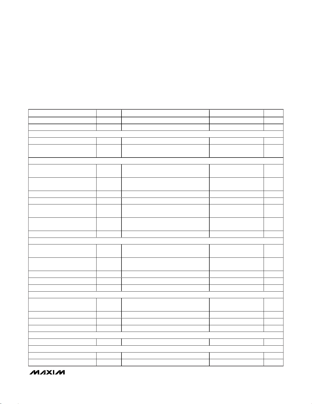
SIGMA-DELTA ADC
Resolution N 16 Bits
Integral Nonlinearity INL -16 ±2 LSB
Differential Nonlinearity DNL Guaranteed monotonic -1 +1 LSB
Offset Error OE -35 +35 mV
Offset-Error Drift ±30 µV/°C
Gain Error GE Trimmed with 150Ω/330pF anti-alias filter -1 +1 %
Gain Temperature Coefficient ±50 ppm/°C
Channel Gain-Error Matching Complete analog signal path -0.25 +0.25 %
Channel Offset Matching Complete analog signal path -60 +60 mV
DYNAMIC PERFORMANCE (PGA Disabled, PGA Gain = 1 x (25kHz -1dB Full-Scale Signal))
Maximum Full-Scale Input ADC modulator gain = 1 1.2 V
Input-Referred Noise Spectral
Density
Second Harmonic to
Fundamental
Third Harmonic to Fundamental -80 -110 dB
Spurious-Free Dynamic Range SFDR 77 102 dB
Channel-to-Channel Isolation
Channel Phase Matching
PARAMETER SYMBOL CONDITIONS MIN TYP MAX UNITS
100kHz 85 nV/√Hz
Unused channels are shorted and
unconnected
Between all channels, including complete
analog signal path
-80 -93 dB
85 108 dB
-0.05 +0.05 Degrees
P-P
Page 3
MAX11043
4-Channel, 16-Bit, Simultaneous-Sampling ADCs
with PGA, Filter, and 8-/12-Bit Dual-Stage DAC
_______________________________________________________________________________________ 3
ELECTRICAL CHARACTERISTICS (continued)
((V
AVDD
= +3.0V to +3.6V, V
DVDD
= +3.0V, C
DVREG
= 10µF, V
AGND
= V
DGND
= 0, common-mode input voltage = AVDD/2, V
REFBP
=
V
REFA
= V
REFB
= V
REFC
= V
REFD
= +2.5V (external reference), V
REFDAC
= V
REFDACH
= +1.25V (external reference), V
REFDACL
= 0,
C
REFBP
= C
REFA
= C
REFB
= C
REFC
= C
REFD
= C
REFDAC
= 1µF, f
SCLK
= 38.4MHz, f
EXCLK
= 38.4MHz (external clock applied to
OSCIN), clock divider set to 4, SHDN = DACSTEP = UP/DWN = DGND, CONVRUN = DVDD, all analog inputs driven directly through
a series 150Ω/330pF anti-alias filter, PGA gain = 1. Default filters and gain settings. T
A
= T
MIN
to T
MAX
, unless otherwise noted (Note 1).
Typical values are at T
A
= +25°C.)
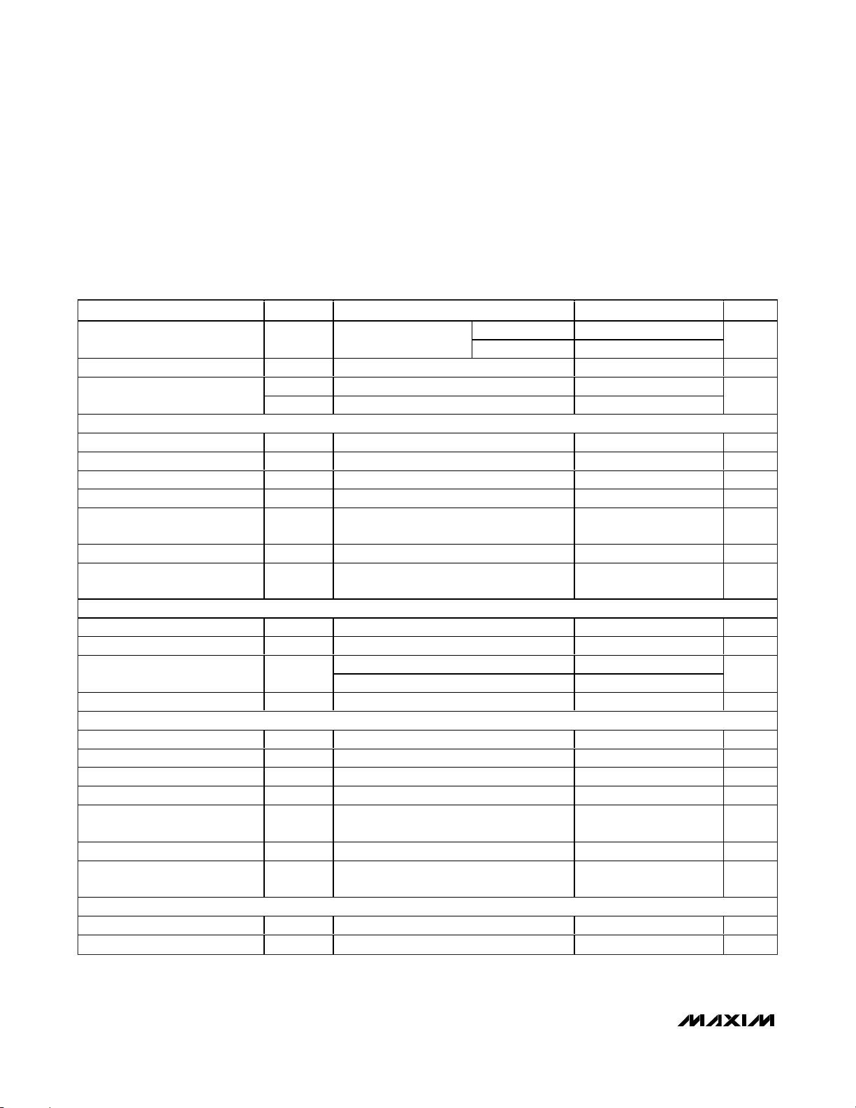
DYNAMIC PERFORMANCE (PGA Enabled, PGA Gain = 8 x (25kHz -1dB Full-Scale Signal))
Maximum Full-Scale Input ADC modulator gain = 1 150 mV
Input-Referred Noise Spectral
Density
Second Harmonic to
Fundamental
Third Harmonic to Fundamental -94 dB
Spurious-Free Dynamic Range SFDR 100 dB
Channel-to-Channel Isolation
Channel Phase Matching
DYNAMIC PERFORMANCE (PGA Enabled, PGA Gain = 16 x (25kHz -1dB Full-Scale Signal))
Maximum Full-Scale Input ADC modulator gain = 1 75 mV
Input-Referred Noise Spectral
Density
Second Harmonic to
Fundamental
Third Harmonic to Fundamental -93 dB
Spurious-Free Dynamic Range SFDR 97 dB
Channel-to-Channel Isolation
Channel Phase Matching
DYNAMIC PERFORMANCE (EQ Mode (5kHz -1dB Full-Scale Signal, CONFIG_ Register Bit 3 = 1))
Maximum Full-Scale Input ADC modulator gain = 1 (Note 2) 800 mV
Input-Referred Noise Spectral
Density
Second Harmonic to
Fundamental
Third Harmonic to Fundamental -77 -98 dB
Spurious-Free Dynamic Range SFDR Input referred (Note 3) 80 89 dB
PARAMETER SYMBOL CONDITIONS MIN TYP MAX UNITS
100kHz 20 nV/√Hz
Unused channels are shorted and
unconnected
Between all channels, including complete
analog signal path
100kHz 15 nV/√Hz
Unused channels are shorted and
unconnected
Between all channels, including complete
analog signal path
100kHz 6 nV/√Hz
-92 dB
110 dB
-0.05 +0.05 Degrees
-99 dB
106 dB
-0.075 +0.075 Degrees
-80 -90 dB
P-P
P-P
P-P
Page 4
MAX11043
4-Channel, 16-Bit, Simultaneous-Sampling ADCs
with PGA, Filter, and 8-/12-Bit Dual-Stage DAC
4 _______________________________________________________________________________________
ELECTRICAL CHARACTERISTICS (continued)
((V
AVDD
= +3.0V to +3.6V, V
DVDD
= +3.0V, C
DVREG
= 10µF, V
AGND
= V
DGND
= 0, common-mode input voltage = AVDD/2, V
REFBP
=
V
REFA
= V
REFB
= V
REFC
= V
REFD
= +2.5V (external reference), V
REFDAC
= V
REFDACH
= +1.25V (external reference), V
REFDACL
= 0,
C
REFBP
= C
REFA
= C
REFB
= C
REFC
= C
REFD
= C
REFDAC
= 1µF, f
SCLK
= 38.4MHz, f
EXCLK
= 38.4MHz (external clock applied to
OSCIN), clock divider set to 4, SHDN = DACSTEP = UP/DWN = DGND, CONVRUN = DVDD, all analog inputs driven directly through
a series 150Ω/330pF anti-alias filter, PGA gain = 1. Default filters and gain settings. T
A
= T
MIN
to T
MAX
, unless otherwise noted (Note 1).
Typical values are at T
A
= +25°C.)
Channel-to-Channel Isolation
Channel Phase Matching
DYNAMIC PERFORMANCE (All Modes)
Conversion Rate
Minimum Throughput 5 ksps
Power-Supply Rejection Ratio DCPSRR 50 dB
ANALOG INPUTS (AINAP/AINAN, AINBP/AINBN, AINCP/AINCN, AINDP/AINDN)
Absolute Voltage Any Input (Note 4) 0 AVDD V
Input Impedance (Note 5)
Input Capacitance EQ mode only 50 pF
EQ FILTER (Analog and Digital)
Unity-Gain Frequency Default 5 kHz
Lower Transition Frequency Default, from 40dB/decade to 0dB/decade 190 kHz
Upper Transition Frequency Default, from 0dB/decade to -80dB/decade 205 kHz
LP FILTER
-3dB Corner Frequency Default 205 kHz
REFERENCE INPUT
REF_ Input Voltage Range V
Input Current 150 µA
REFBP Input Voltage Range V
Input Current 700 µA
REFDAC Input Voltage Range V
Input Resistance 17 kΩ
PARAMETER SYMBOL CONDITIONS MIN TYP MAX UNITS
REFBP
REFDAC
REF_
Unused channels are shorted and
unconnected
Between all channels, including complete
analog signal path
All 4 channels 400
2 channels only 800
Direct input to ADC,
gain = 1
Direct input to ADC, gain = 2 7
Direct input to ADC, gain = 4 or 8 7
PGA gain = 16 5.5
DIFF = 1 25
DIFF = 0 100
80 104 dB
-0.12 +0.12 Degrees
2 2.5 2.8 V
2 2.5 2.8 V
1 1.25 1.4 V
ksps
kΩ
Page 5
MAX11043
4-Channel, 16-Bit, Simultaneous-Sampling ADCs
with PGA, Filter, and 8-/12-Bit Dual-Stage DAC
_______________________________________________________________________________________ 5
ELECTRICAL CHARACTERISTICS (continued)
((V
AVDD
= +3.0V to +3.6V, V
DVDD
= +3.0V, C
DVREG
= 10µF, V
AGND
= V
DGND
= 0, common-mode input voltage = AVDD/2, V
REFBP
=
V
REFA
= V
REFB
= V
REFC
= V
REFD
= +2.5V (external reference), V
REFDAC
= V
REFDACH
= +1.25V (external reference), V
REFDACL
= 0,
C
REFBP
= C
REFA
= C
REFB
= C
REFC
= C
REFD
= C
REFDAC
= 1µF, f
SCLK
= 38.4MHz, f
EXCLK
= 38.4MHz (external clock applied to
OSCIN), clock divider set to 4, SHDN = DACSTEP = UP/DWN = DGND, CONVRUN = DVDD, all analog inputs driven directly through
a series 150Ω/330pF anti-alias filter, PGA gain = 1. Default filters and gain settings. T
A
= T
MIN
to T
MAX
, unless otherwise noted (Note 1).
Typical values are at T
A
= +25°C.)
PARAMETER SYMBOL CONDITIONS MIN TYP MAX UNITS
REFDAC_ Input Voltage Range V
REFDAC_
0 1.4 V
Input Resistance 150 kΩ
INTERNAL REFERENCE
Reference Voltage V
Reference Temperature
Coefficient
REFBP
2.45 2.5 2.55 V
100 ppm/°C
CRYSTAL OSCILLATOR (Max ESR 100Ω, 22pF Load Capacitors to DGND)
Maximum Crystal Operating
Frequency
External Clock Input Frequency
Range
Epson Electronics MA-505 (16MHz) 16 MHz
External clock applied to OSCIN 4 40 MHz
Stability Excluding crystal 25 ppm
Startup Time Epson Electronics MA-505 (16MHz) 10 ms
OSCIN Input Low Voltage When driven with external clock source
OSCIN Input High Voltage When driven with external clock source
0.7 x
DVDD
0.3 x
DVDD
OSCIN Leakage Current -5 +5 µA
DIGITAL INPUTS
Input High Voltage V
Input Low Voltage V
IH
IL
0.7 x
DVDD
0.3 x
DVDD
Input Hysterisis 15 mV
Input Leakage Current I
Input Capacitance C
IN
V
= 0 or DVDD -1 +1 µA
IN
IN
15 pF
DIGITAL OUTPUTS
DVDD
-
Output-Voltage High V
Output-Voltage Low V
OH
OL
I
I
= 0.8mA
SOURCE
= 1.6mA 0.4 V
SINK
0.6
Three-State Leakage Current DOUT only -1 +1 µA
Three-State Output Capacitance DOUT only 15 pF
VOLTAGE REGULATOR
Regulated Digital Supply Voltage DV
REG
Internal use only 2.5 V
POWER REQUIREMENTS
Analog Supply Voltage 3.0 3.6 V
Digital Supply Voltage 3.0 3.6 V
V
V
V
V
V
Page 6
MAX11043
4-Channel, 16-Bit, Simultaneous-Sampling ADCs
with PGA, Filter, and 8-/12-Bit Dual-Stage DAC
6 _______________________________________________________________________________________
ELECTRICAL CHARACTERISTICS (continued)
((V
AVDD
= +3.0V to +3.6V, V
DVDD
= +3.0V, C
DVREG
= 10µF, V
AGND
= V
DGND
= 0, common-mode input voltage = AVDD/2, V
REFBP
=
V
REFA
= V
REFB
= V
REFC
= V
REFD
= +2.5V (external reference), V
REFDAC
= V
REFDACH
= +1.25V (external reference), V
REFDACL
= 0,
C
REFBP
= C
REFA
= C
REFB
= C
REFC
= C
REFD
= C
REFDAC
= 1µF, f
SCLK
= 38.4MHz, f
EXCLK
= 38.4MHz (external clock applied to
OSCIN), clock divider set to 4, SHDN = DACSTEP = UP/DWN = DGND, CONVRUN = DVDD, all analog inputs driven directly through
a series 150Ω/330pF anti-alias filter, PGA gain = 1. Default filters and gain settings. T
A
= T
MIN
to T
MAX
, unless otherwise noted (Note 1).
Typical values are at T
A
= +25°C.)
Analog Supply Current I
Digital Supply Current I
Shutdown Current
STATIC ACCURACY—FINE DAC (CL = 200pF, RL = 10kΩ)
Resolution 12 Bits
Integral Nonlinearity INL -5 +5 LSB
Differential Nonlinearity DNL Guaranteed monotonic -1 +1 LSB
Offset Error -70 +70 mV
Offset-Error Temperature
Coefficient
Gain Error -2 0 %
Gain-Error Temperature
Coefficient
DYNAMIC PERFORMANCE—FINE DAC (CL = 200pF, RL = 10kΩ)
Output Noise f = 0.1Hz to 1MHz 200 µV
DAC Glitch Impulse Major carry transition 12 nV•s
Voltage-Output Settling Time
Voltage-Output Slew Rate 0.6 V/µs
STATIC ACCURACY—REFDACH AND REFDACL
Resolution 8 Bits
Integral Nonlinearity INL -0.5 +0.5 LSB
Differential Nonlinearity DNL -0.2 +0.2 LSB
Offset Error -30 +30 mV
Offset-Error Temperature
Coefficient
Gain Error -5 +5 LSB
Gain-Error Temperature
Coefficient
FLASH MEMORY
Programming Endurance 10,000 Cycles
Data Retention TA = +85°C 15 Years
PARAMETER SYMBOL CONDITIONS MIN TYP MAX UNITS
AVDD
DVDD
I
AVDD
I
DVDD
All channels selected
25% to 75% FS 3
1% FS 1.5
PGA disabled 60 80
PGA enabled 120 140
26 40 mA
±50 µV/°C
±20
±50 µV/°C
5
5
±20
mA
mA
ppm of
FS/°C
RMS
µs
ppm of
FS/°C
Page 7
MAX11043
4-Channel, 16-Bit, Simultaneous-Sampling ADCs
with PGA, Filter, and 8-/12-Bit Dual-Stage DAC
_______________________________________________________________________________________ 7
Note 1: Devices 100% production tested at TA= +125°C. Guaranteed by design and characterization to TA= -40°C.
Note 2: Full scale in analog EQ mode decreases with increasing frequency at a rate of 20dB/decade from 5kHz. If digital EQ is also
used, full scale decreases with increasing frequency at 40dB/decade from 5kHz.
Note 3: SFDR in the EQ mode is normalized to the input by subtracting the analog EQ gain at each frequency (20dB/decade) from
the FFT results.
Note 4: The absolute input voltage range is 0 to AVDD. For optimal performance, use a common-mode voltage of AVDD/2.
Note 5: Switched capacitor input impedance is proportional to 1/fC. Where f is the sampling frequency and C is the input capacitance.
ELECTRICAL CHARACTERISTICS (continued)
((V
AVDD
= +3.0V to +3.6V, V
DVDD
= +3.0V, C
DVREG
= 10µF, V
AGND
= V
DGND
= 0, common-mode input voltage = AVDD/2, V
REFBP
=
V
REFA
= V
REFB
= V
REFC
= V
REFD
= +2.5V (external reference), V
REFDAC
= V
REFDACH
= +1.25V (external reference), V
REFDACL
= 0,
C
REFBP
= C
REFA
= C
REFB
= C
REFC
= C
REFD
= C
REFDAC
= 1µF, f
SCLK
= 38.4MHz, f
EXCLK
= 38.4MHz (external clock applied to
OSCIN), clock divider set to 4, SHDN = DACSTEP = UP/DWN = DGND, CONVRUN = DVDD, all analog inputs driven directly through
a series 150Ω/330pF anti-alias filter, PGA gain = 1. Default filters and gain settings. T
A
= T
MIN
to T
MAX
, unless otherwise noted (Note 1).
Typical values are at T
A
= +25°C.)
Typical Operating Characteristics
(V
AVDD
= +3.3V, V
DVDD
= +3.0V, f
SCLK
= f
EXCLK
= 19.2MHz, V
REFBP
, V
REF_
= +2.5V, common-mode input voltage = AVDD/2,
TA = +25°C, unless otherwise noted.)
INL vs. CODE
MAX11043 toc01
CODE (LSB)
INL (LSB)
491523276816384
-4
-3
-2
-1
0
1
2
3
4
5
-5
0 65536
LP MODE
GAIN = 1
400ksps FFT
LP MODE
MAX11043 toc02
FREQUENCY (kHz)
AMPLITUDE (dBFS)
18016014012010080604020
-100
-80
-60
-40
-20
0
-120
0 200
fIN = 50kHz
GAIN = 1
800ksps FFT
LP MODE
MAX11043 toc03
FREQUENCY (kHz)
AMPLITUDE (dBFS)
35030025020015010050
-120
-100
-80
-60
-40
-20
0
-140
0400
fIN = 50kHz
GAIN = 1
PARAMETER SYMBOL CONDITIONS MIN TYP MAX UNITS
SPI INTERFACE
SCLK Clock Period t
SCLK Pulse-Width High t
SCLK Pulse-Width Low t
SCLK Rise to DOUT Transition t
CS Fall to SCLK Rise Setup Time t
SCLK Rise to CS Rise Setup Time t
DIN to SCLK Rise Setup Time t
DIN to SCLK Rise Hold Time t
CS Pulse-Width High t
CS Rise to DOUT Disable t
CS Fall to DOUT Enable t
EOC Fall to CS Fall t
CP
CH
CL
DOT
CSS
CSH
DS
DH
CSPWH
DOD
DOE
RDS
C
= 20pF 1 15 ns
LOAD
= 20pF 20 ns
C
LOAD
C
= 20pF 1 ns
LOAD
25 ns
10 ns
10 ns
10 ns
5ns
10 ns
0ns
10 ns
10 ns
Page 8
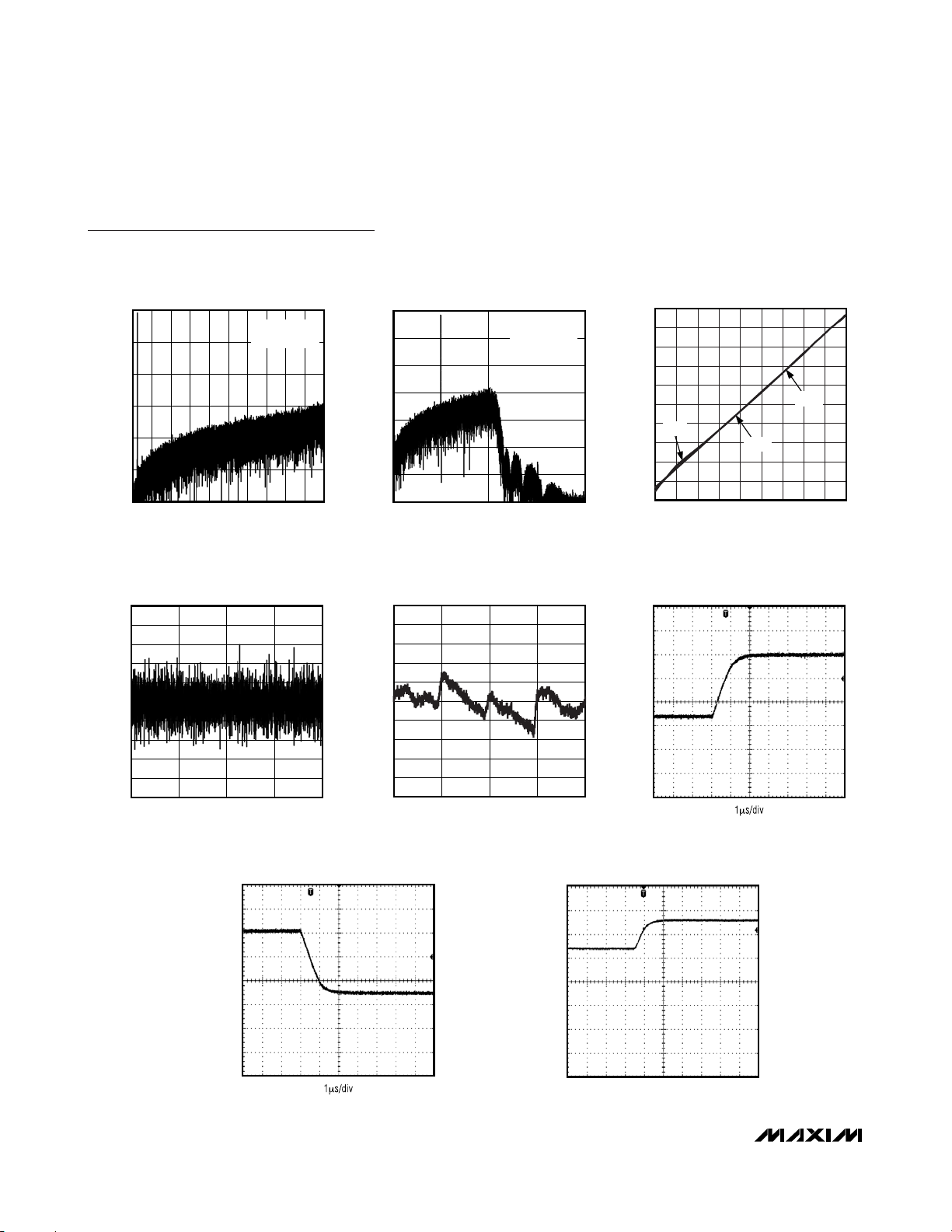
FINE DAC SETTLING
75% TO 25% FS STEP
MAX11043 toc10
500mV/div
0V
FINE DAC SETTLING
1% STEP-UP
MAX11043 toc11
1μs/div
20mV/div
1200mV
MAX11043
4-Channel, 16-Bit, Simultaneous-Sampling ADCs
with PGA, Filter, and 8-/12-Bit Dual-Stage DAC
8 _______________________________________________________________________________________
Typical Operating Characteristics (continued)
(V
AVDD
= +3.3V, V
DVDD
= +3.0V, f
SCLK
= f
EXCLK
= 19.2MHz, V
REFBP
, V
REF_
= +2.5V, common-mode input voltage = AVDD/2,
T
A
= +25°C, unless otherwise noted.)
400ksps FFT
EQ MODE
0
fIN = 5kHz
V
= 560mV
-20
-40
-60
AMPLITUDE (dBFS)
-80
-100
-120
0200
FREQUENCY (kHz)
INP-P
MAX11043 toc04
18016014012010080604020
0
-20
-40
-60
-80
AMPLITUDE (dBFS)
-100
-120
-140
0 400200
800ksps FFT
EQ MODE
FREQUENCY (kHz)
SINAD vs. INPUT AMPLITUDE
80
fIN = 100kHz
V
INP-P
= 1.4mV
MAX11043 toc05
70
60
50
40
30
SINAD (dB)
20
1kHz
10
0
-10
-20
-90 0
10kHz
INPUT AMPLITUDE (dBFS)
MAX11043 toc06
50kHz
-10-30-70 -50 -20-40-80 -60
1.0
0.8
0.6
0.4
0.2
0
DNL (LSB)
-0.2
-0.4
-0.6
-0.8
-1.0
0 4096
FINE DAC DNL
vs. CODE
CODE (LSB)
FINE DAC INL
vs. CODE
5
4
MAX11043 toc07
307220481024
3
2
1
0
INL (LSB)
-1
-2
-3
-4
-5
0 4096
CODE (LSB)
307220481024
MAX11043 toc08
FINE DAC SETTLING
25% TO 75% FS STEP
MAX11043 toc09
500mV/div
0V
Page 9
MAX11043
FINE DAC SETTLING
1% STEP-DOWN
MAX11043 toc12
1μs/div
20mV/div
1200mV
4-Channel, 16-Bit, Simultaneous-Sampling ADCs
with PGA, Filter, and 8-/12-Bit Dual-Stage DAC
_______________________________________________________________________________________ 9
COARS
Typical Operating Characteristics (continued)
(V
AVDD
= +3.3V, V
DVDD
= +3.0V, f
SCLK
= f
EXCLK
= 19.2MHz, V
REFBP
, V
REF_
= +2.5V, common-mode input voltage = AVDD/2,
T
A
= +25°C, unless otherwise noted.)
POWER-ON RESET
vs. TEMPERATURE
MAX11043 toc19
TEMPERATURE (°C)
SUPPLY VOLTAGE (V)
12010060 8002040-20
0.2
0.4
0.6
0.8
1.0
1.2
1.4
1.6
1.8
2.0
0
-40
ANALOG SUPPLY
DIGITAL SUPPLY
E DAC INL
vs. CODE
0.5
CODES 3 TO 255
0.4
0.3
0.2
0.1
0
INL (LSB)
-0.1
-0.2
-0.3
-0.4
-0.5
0 256
DACL
CODE (LSB)
DACH
MAX11043 toc15
19212864
FINE DAC NOISE FLOOR
0
FREQUENCY (kHz)
COARSE DAC SETTLING TIME,
POSITIVE STEP
2ms/div
1401201004020 1801608060 200
COARSE DAC DNL
MAX11043 toc13
0dBm
20dBm/div
1.0
CODES 3 TO 255
0.8
0.6
0.4
0.2
0
DNL (LSB)
-0.2
-0.4
-0.6
-0.8
-1.0
0256
vs. CODE
DACH
DACL
CODE (LSB)
COARSE DAC SETTLING TIME,
MAX11043 toc16
200mV/div
NEGATIVE STEP
2ms/div
MAX11043 toc14
19212864
MAX11043 toc17
200mV/div
DVREG VOLTAGE vs. TEMPERATURE
2.369
2.368
2.367
2.366
2.365
DVREG VOLTAGE (V)
2.364
2.363
2.362
-40
TEMPERATURE (°C)
MAX11043 toc18
120100806040200-20
Page 10
MAX11043
4-Channel, 16-Bit, Simultaneous-Sampling ADCs
with PGA, Filter, and 8-/12-Bit Dual-Stage DAC
10 ______________________________________________________________________________________
Pin Description
PIN NAME FUNCTION
1 AINBN Channel B Analog Negative Input
2 REFA Channel A Reference Bypass. Bypass REFA with a nominal 1µF capacitor to AGND.
3 AINAN Channel A Analog Negative Input
4 AINAP Channel A Analog Positive Input
5, 26 AVDD Analog Supply. Bypass each AVDD with a nominal 1µF capacitor to AGND.
6, 24, 33 AGND Analog Ground. Connect AGND inputs together.
7, 23 DGND Digital Ground. Connect DGND inputs together.
8, 22 DVDD Digital Supply. Bypass each DVDD with a nominal 1µF capacitor to DGND.
9 DVREG Regulated Digital Core Supply. Bypass DVREG to DGND with a 10µF capacitor.
10 UP/DWN DAC Step Direction Select. Drive high to step up, drive low to step down when DACSTEP is toggled.
11 DACSTEP
12 CONVRUN
13 CS Active-Low Serial-Interface Chip Select
14 DOUT Serial-Interface Data Out. Data transitions on the rising edge of SCLK.
15 DIN Serial-Interface Data In. Data is sampled on the rising edge of SCLK.
16 SCLK Serial-Interface Clock
17, 35 I.C. Internally Connected. Connect to either AGND or DGND.
18 EOC Active-Low End-of-Conversion Indicator. EOC asserts low to indicate that new data is ready.
19 OSCIN Crystal Oscillator/External Clock Input
20 OSCOUT Crystal-Oscillator Output. Leave unconnected when using external clock.
21 SHDN Active-High Shutdown Input. Drive high to shut down the MAX11043.
25 AOUT Buffered 12-Bit Fine DAC Output
27 REFDACL Fine DAC Low Reference Bypass. Bypass REFDACL with a nominal 1µF capacitor to AGND.
28 REFDACH Fine DAC High Reference Bypass. Bypass REFDACH with a nominal 1µF capacitor to AGND.
29 REFDAC Coarse DAC Reference Bypass. Bypass REFDAC with a nominal 1µF capacitor to AGND.
30 REFD Channel D Reference Bypass. Bypass REFD with a nominal 1µF capacitor to AGND.
31 AINDN Channel D Analog Negative Input
32 AINDP Channel D Analog Positive Input
34 REFBP Main Reference Bypass. Bypass REFBP with a nominal 1µF capacitor to AGND.
36 AINCN Channel C Analog Negative Input
37 AINCP Channel C Analog Positive Input
38 REFC Channel C Reference Bypass. Bypass REFC with a nominal 1µF capacitor to AGND.
39 REFB Channel B Reference Bypass. Bypass REFB with a nominal 1µF capacitor to AGND.
40 AINBP Channel B Analog Positive Input
—EP
DAC Step Input. Drive high to move the DAC output in the direction of UP/DWN on the next rising
edge of the system clock.
Convert Run. Drive high to start continuous conversions on all 4 channels. The device is idle when
CONVRUN is low.
Exposed Pad. Connect EP to a ground plane on the PCB to enhance thermal dissipation. Internally
connected to AGND. Not intended as an electrical connection point.
Page 11

MAX11043
4-Channel, 16-Bit, Simultaneous-Sampling ADCs
with PGA, Filter, and 8-/12-Bit Dual-Stage DAC
______________________________________________________________________________________ 11
Functional Diagram
AINAP
AINAN
REFA
AINBP
AINBN
REFB
AINCP
AINCN
PGA
EQ
PGA
EQ
PGA
EQ
SIGMA-DELTA
ADC
SIGMA-DELTA
ADC
SIGMA-DELTA
ADC
PROGRAMMABLE
DIGITAL FILTER
PROGRAMMABLE
DIGITAL FILTER
MAX11043
PROGRAMMABLE
DIGITAL FILTER
AVDD
DVDD
UP/DWN
DACSTEP
CONVRUN
SERIAL
INTERFACE
FLASH
POR
EOC
SHDN
SCLK
DOUT
DIN
REFC
AINDP
AINDN
REFD
DIGITAL SUPPLY
+2.5V
VOLTAGE
REFERENCE
PGA
EQ
R
R
SIGMA-DELTA
ADC
8-BIT
DAC
PROGRAMMABLE
DIGITAL FILTER
REFDACHREFDACLREFDACREFBP
12-BIT DAC
2x
AOUT
INTERNAL
REGULATOR
+2.5V
CLOCK
CRYSTAL
OSCILLATOR
AND CLOCK
BUFFER
AGND DGND
DVREG
OSCOUT
OSCIN
Page 12

MAX11043
4-Channel, 16-Bit, Simultaneous-Sampling ADCs
with PGA, Filter, and 8-/12-Bit Dual-Stage DAC
12 ______________________________________________________________________________________
Detailed Description
The MAX11043 features 4 single-ended or differential
channels of simultaneous-sampling ADCs with 16-bit
resolution. The MAX11043 contains a versatile filter
block and PGA per channel. The filter consists of seven
cascaded 2nd-order filter sections for each channel
allowing the construction of a 14th-order filter. The filter
coefficients are user-programmable. Configure each
2nd-order filter as a LP filter, HP filter, or BP filter with
optional rectification. Gain and phase mismatch of the
analog signal path is better than -50dB.
The ADCs can sample up to 800ksps per channel. A
40MHz serial interface provides communication to and
from the device. The SPI interface provides throughput
of 1600ksps; 4 channels at 400ksps per channel or 2
channels at 800ksps per channel. A software-selectable scan mode allows reading the ADC results while
simultaneously updating the DAC. Other features of the
MAX11043 include an internal (+2.5V) or external
(+2.0V to +2.8V) reference, power-saving modes, and
a PGA with gains of 1 to 64. The PGA includes an EQ
function that automatically boosts low-amplitude, highfrequency signals for applications such as CW-chirp
radar.
The MAX11043 includes two 8-bit coarse DACs that set
the high and low references for a second-stage 12-bit
fine DAC, typically used for VCO control. Use software
controls to set the DAC, or step the DAC up and down
using hardware control in programmable steps.
MAX11043 Signal Path
Each of the 4 ADC channels features a PGA and filter
block that feeds the signal to the sigma-delta modulator. The PGA can either be bypassed, which provides a
gain of 1, set to a gain of 8, a gain of 16, or set to analog EQ mode. For more amplification, set the ADC modulator gain to one, two, or four. After the modulator, the
result passes through the sinc 5 filter and decimator.
Seven biquad programmable digital filters isolate the
band of interest. Read the result using the 40MHz SPI
interface. See Figure 1.
Analog-to-Digital Converter
The MAX11043 features a quad sigma-delta ADC architecture with 4 differential input channels. For singleended operation, connect the N input to the
common-mode voltage or bypass to AGND with a 10µF
capacitor. All inputs feature a programmable bias generator; see the
CONFIG_ Register (0Ch–0Fh)
section.
All four ADCs convert simultaneously with a maximum
modulator sampling rate of 9.6Msps; decimated by 12
or 24 for output rates of 800ksps and 400ksps, respectively. The SPI bus limits the maximum output data rate
to 40Mbps.
Sinc 5 Filter
The sinc 5 filter removes high-frequency noise from the
output of the sigma-delta modulator. It also decimates
the modulator data by a factor of 12, providing a maximum of 800ksps to the programmable filters when the
modulator is operating at 9.6Msps. Figure 2 shows the
frequency characteristics of the sinc 5 filter with the
modulator running at 9.6Msps. Operating the modulator
PGA AND
FILTER
MODULATOR
WITH GAINS OF
1, 2, OR 4
SINC 5 FILTER AND
DECIMATE BY 12
SPI
BIQUAD
FILTER 1
BIQUAD
FILTER 7
IN
7 BIQUAD FILTERS IN SERIES
MODG1 MODG0
0 0
0 1
1 0
1 1
GAIN
1
2
4
4EQUALIZER
LP FILTER AND GAIN 16X
LP FILTER AND GAIN 8X
BYPASS
PGA AND FILTER MODES
PDPGA PGAG EQ
1 X X
0 0 0
0 1 0
0 X 1
FINE
GAIN
ADJUST
CHAN X FINE GAIN
RESOLUTION = 16 BITS
RAM
POR VALUES
POR VALUES
USER VALUESUSER DEFINED
EQUALIZER
LP FILTER
BIQUAD MODES FILT
1
0
X
RANGE: -4 TO +4
DECIMATE
BY 1 OR 2
DECIMATE
TOTAL
DECIMATION
2 24
1 12
DECSEL
0
1
Figure 1. Signal Path
Page 13

MAX11043
4-Channel, 16-Bit, Simultaneous-Sampling ADCs
with PGA, Filter, and 8-/12-Bit Dual-Stage DAC
______________________________________________________________________________________ 13
at a lower sample rate causes a proportional reduction
in the frequency response of the sinc 5 filter. The total
attenuation of the MAX11043 is the sum of the analog
filtering, the sinc 5 filter, and the seven stages of programmable filters.
Equalizer (EQ)
The EQ matches the frequency/gain characteristics of
CW-chirp radar systems where the distance to the target is proportional to the measured frequency. Distant
targets not only have a higher frequency, they have a
weaker signal. Hence, higher frequencies need more
amplification than lower frequencies. The EQ provides
gain proportional to frequencies up to 190kHz, at which
point the gain rolls off at 80dB/decade.
The EQ consists of an analog section in the PGA and a
digital EQ created from the biquad filters. The analog
EQ (PGA) provides 20dB/decade of gain and the
default digital EQ provides an additional 20dB/decade
of gain. Together they provide 40dB/decade of gain up
to 190kHz with a gain of 0dB at 5kHz.
Variations in the manufacturing process affect the gain
and phase of the analog filter. Compensation for these
variations include adjustments to the digital filter during
the manufacture of the MAX11043. Use the analog and
digital EQs together for optimal performance. For a
detailed description of digital-filter customization, refer
to the
MAX11043 User’s Guide
.
Conversion and ADC Reading
Drive CONVRUN high to initiate a continuous conversion on all 4 channels. Keep CONVRUN high for the
entire conversion process. Do not pulse CONVRUN.
EOC asserts low when new data is available. Initiate a
data read prior to the next rising edge of EOC or the
result is overwritten. EOC asserts high upon read completion of all active channels. Use ConfigA, ConfigB,
ConfigC, and ConfigD registers to read single channel
data. Concatenated data is available in the ADCAB,
ADCCD, and ADCABCD registers. Use concatenated
registers to ensure simultaneous results are read. See
the
Register Functions
section for more details.
A software-selectable scan mode automatically sends
the result from selected channels following the CS
falling edge and allows other registers to be simultaneously updated. To enable scan mode, set SCHAN_ bits
high. See the
Configuration Register (08h)
section for a
detailed description. The ADC output is presented in
two’s complement format (Figure 3).
Digital Filter
Seven cascaded, individually configurable, 2nd-order
filter elements make up the digital filter. Figure 4 shows
the structure of a single filter section. Configure these
elements as LP, BP, HP, or all pass (AP) filters with
optional rectification. Filter configuration is transferred
from the flash to coefficient RAM (C-RAM) on power-up.
Store custom filters permanently in the flash or write
directly to C-RAM each time on power-up. Two separate sets of programmable coefficients exist for each
filter. Dual coefficient sets allow rapid filter reconfiguration. These filter coefficients are programmed to LP and
EQ modes at the factory. Multiple flash memory pages
exist so that custom filters can be created while preserving factory-programmed filter coefficients.
SINC 5 FILTER AT 9.6Msps
MAX11043 fig02
FREQUENCY (kHz)
ATTENUATION (dB)
16001200800400
-100
-80
-60
-40
-20
0
-120
0 2000
Figure 2. Sinc 5 Filter Frequency Response
0 +1 +FS-1-FS
1000 0000 0000 0000
1000 0000 0000 0001
1000 0000 0000 0010
INPUT VOLTAGE (LSB)
BINARY OUTPUT CODE
0111 1111 1111 1101
0111 1111 1111 1110
0111 1111 1111 1111
0000 0000 0000 0000
0000 0000 0000 0001
1111 1111 1111 1111
Figure 3. Two’s Complement Transfer Function
Page 14

MAX11043
4-Channel, 16-Bit, Simultaneous-Sampling ADCs
with PGA, Filter, and 8-/12-Bit Dual-Stage DAC
14 ______________________________________________________________________________________
Filter coefficients A1 and B1 are always 1. B3 is limited
to -1, 0, and 1.
Filter coefficients A2, A3, and B2 are stored as 16-bit
two’s complement values in the range of -4 to +4.
Gain is limited to the following values 2
4
, 22, 20, 2-2, 2-4,
2
-6
, 2-8, and 2
-10
. For better gain resolution, adjust the
Fine Gain A/B/C/D Registers at the input of each filter
set. Fine gain adjustment has a resolution of 16 bits and
a gain range of -4 to +4. Set the RECT bit to rectify the
filter output.
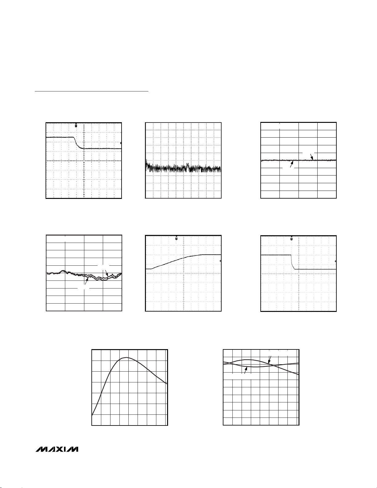
Figures 5–8 show the response to a step input of the
default filters used for ADC trimming.
1/A1
-A2
Z
-1
-A3
B1
B2
B3
+
+
+
+
OUT
IN
X
Y
RECT
G
ABS
Z
-1
Figure 4. Single Programmable 2nd-Order Filter Section
SINC 5 FILTER OUTPUT
MAX11043 fig05
SAMPLE
OUTPUT (LSB)
8642
500
1000
1500
2000
2500
0
010
Figure 5. Sinc 5 Filter Response to a Step Input
Page 15

MAX11043
4-Channel, 16-Bit, Simultaneous-Sampling ADCs
with PGA, Filter, and 8-/12-Bit Dual-Stage DAC
______________________________________________________________________________________ 15
Programmable Gain Amplifier
Each ADC channel features an input buffer with input
impedance of at least 5kΩ and programmable gain of
eight or 16. When set to a gain of one, the signal
bypasses the PGA to reduce noise.
The PGA features an optional 20dB/decade analog EQ
mode, with a gain of 0dB at 5kHz and attenuation
above 190kHz to reduce out-of-band noise. Using the
digital EQ filter adds another 20dB/decade gain.
Control the EQ and PGA gain from their respective
CONFIG_ registers. For additional filtering and equalization, use the integrated digital filters. Refer to the
MAX11043 User’s Guide
for more information.
Digital-to-Analog Converter
The MAX11043 features a 12-bit fine DAC with high and
low reference inputs set by the 8-bit, dual tap coarse DAC
or driven externally. The output buffer of the fine DAC has
a gain of two and can drive 10kΩ and 200pF in parallel.
Bypass the REFDACH and REFDACL with a 1µF capacitor when using the coarse DAC to set the reference
values, or power down the buffers and drive REFDACH
and REFDACL with external references. Alternatively
drive one of the fine DAC references using the coarse
DAC and the other using an external reference.
The fine DAC register contains the current value of the
output. The output value changes by writing to this register or by the rising edge of the DACSTEP input. The
DAC register updates on the next rising edge of the
system clock following the rising edge of the DACSTEP
input. The programmable DACSTEP register contains
the step size. The UP/DWN input sets the direction of
the step. Drive UP/DWN high to step up, drive low to
step down.
The coarse 8-bit, dual tap DAC generates the high and
low reference values for the fine DAC. Obtain the
coarse DAC reference from the main reference or by
driving the REFDAC input externally. The main reference, REFBP, is divided by two before the coarse DAC.
When driving REFDAC, REFDACH, or REFDACL directly, ensure the voltage to the fine DAC does not exceed
AVDD/2 to prevent the output amplifier from saturating.
EQ FILTER OUTPUT
MAX11043 fig06
SAMPLE
OUTPUT (LSB)
806020 40
-15,000
-10,000
-5000
0
5000
10,000
15,000
20,000
25,000
30,000
35,000
-20,000
0100
Figure 6. EQ Filter Response to a Step Input
STAGE 1 FILTER OUTPUT
MAX11043 fig08
SAMPLE
OUTPUT (LSB)
4010 3020
0
500
1000
1500
2000
2500
3000
3500
-500
050
Figure 8. Stage 1 Default Filter Response to a Step Input
LP FILTER OUTPUT
MAX11043 fig07
SAMPLE
OUTPUT (LSB)
80604020
500
1000
1500
2000
2500
0
0100
Figure 7. LP Filter Response to a Step Input
Page 16

MAX11043
4-Channel, 16-Bit, Simultaneous-Sampling ADCs
with PGA, Filter, and 8-/12-Bit Dual-Stage DAC
16 ______________________________________________________________________________________
Reference (REFBP)
The MAX11043 features an internal 2.5V bandgap reference. Bypass REFBP with a 1µF capacitor or power
down the buffer amplifier and drive REFBP with an
external reference. In internal reference mode, REFBP
provides the main reference voltage for the MAX11043.
Refer to www.maxim-ic.com/references for a list of
available precision references.
In addition to the integrated main reference, there are
seven separate references derived from REFBP, one for
each ADC channel, one for the coarse DAC, and two
(one high and one low) for the fine DAC. When using
the main reference, bypass each of the references with
a 1µF capacitor or set the appropriate bits (7–0), in the
reference (10h) register, to power down the references
and drive externally. Use external references capable
of driving a 700µA or total load.
Clock Sources
The MAX11043 features an internal 16MHz oscillator
that supports either an external crystal or ceramic resonator. For highest performance, set bit 15 in the configuration register to 1 and use an external clock (EX
clock) source, up to 40MHz, to drive OSCIN. A programmable clock divider divides the EX clock by 2, 3,
4, or 6 to generate the ADC sample clock. The system
clock, used for all digital timing, is twice the ADC sample clock. Ensure that the minimum EX clock high or
low time is greater than 25ns when using the divide-by2 or divide-by-3 mode.
The system clock, used for all internal timing, is derived
from the clock divider setting and the input clock.
For optimal performance, derive the SPI clock and system clock from the same source.
Power Saving
The MAX11043 features an active-high power-down
input, as well as an SPI-controlled power-down bit that
places the MAX11043 in low-power mode. In addition,
the MAX11043 features an independent, SPI-controlled,
power-down for each ADC channel, the DAC, and the
oscillator. See the
Configuration Register (08h)
section
for more details.
Serial Communication
The SPI-compatible interface allows synchronous serial
data transfers up to 40Mbps. The bandwidth is divided
between the DACs and the ADC. Maximum conversion
throughput depends on which read commands are
used. The highest conversion rates are obtained by
using the scan mode. The second highest rate is
obtained by reading concatenated registers. The slowest method is to read the results individually.
Configure the SPI master for SCLK to idle low (SCLK is
low when CS is asserted). The data at DIN is latched on
the rising edge of SCLK. Data at DOUT transitions
immediately after the rising edge of SCLK.
All SPI transactions start with a command byte. The
command byte selects the address of the register and
the mode of operation (read/write).
SPI Command Byte
START<7>: Start bit. This bit must be 0 for normal
operation.
ADR_<6:2>: Device register address bits. See the register map in Table 1.
R/W<1>: Read/write bit. 1 = read from device. 0 = write
to device.
BIT 7 BIT 6 BIT 5 BIT 4 BIT 3 BIT 2 BIT 1 BIT 0
START ADR4 ADR3 ADR2 ADR1 ADR0 R/W 0
Page 17

MAX11043
4-Channel, 16-Bit, Simultaneous-Sampling ADCs
with PGA, Filter, and 8-/12-Bit Dual-Stage DAC
______________________________________________________________________________________ 17
Figure 9. SPI 8-Bit Write Operation
Figure 10. SPI 8-Bit Read Operation
t
START
DS
t
DH
ADR 3 ADR 2
CS
SCLK
DIN
DOUT
t
CSS
X
HIGH IMPEDANCE
t
SCLK
DIN
CSS
t
DOE
CS
X
START
t
DS
t
ADR 4
DH
ADR 3 ADR 2
t
CP
t
CH
t
CL
ADR 1 ADR 0
t
CP
t
CH
t
CL
ADR 1 ADR 0 R/W = 1
R/W = 0
0ADR 4
D7 D6 D5 D4 D3 D2 D1 D0
t
DOT
X X X
0
X X X X X
t
CSH
HIGH IMPEDANCE
t
DOD
HIGH IMPEDANCE
DOUT
D7 D6 D5 D4 D3 D2 D1 D0
HIGH IMPEDANCE
Page 18

MAX11043
4-Channel, 16-Bit, Simultaneous-Sampling ADCs
with PGA, Filter, and 8-/12-Bit Dual-Stage DAC
18 ______________________________________________________________________________________
Register Map
Table 1. SPI Register Map
ADDRESS REGISTER NAME FUNCTION BITS
00h ADCA ADC channel A result register 16/24
01h ADCB ADC channel B result register 16/24
02h ADCC ADC channel C result register 16/24
03h ADCD ADC channel D result register 16/24
04h ADCAB ADC channels A and B results register 32/48
05h ADCCD ADC channels C and D results register 32/48
06h ADCABCD ADC channels A, B, C, and D results register 64/96
07h Status Status register 8
08h Configuration Configures the device 16
09h DAC Fine DAC value 16
0Ah DACSTEP Step size for DAC increment/decrement function 16
0Bh DACH/DACL High and low coarse DAC values 8 + 8
0Ch ConfigA ADC channel A configuration 16
0Dh ConfigB ADC channel B configuration 16
0Eh ConfigC ADC channel C configuration 16
0Fh ConfigD ADC channel D configuration 16
10h Reference/Delay Sets the operation state of the reference and buffers 16
11h AGain Channel A fine gain 16
12h BGain Channel B fine gain 16
13h CGain Channel C fine gain 16
14h DGain Channel D fine gain 16
15h Filter coefficient address
16h Filter coefficient data out Coefficient RAMs output data 32
17h Filter coefficient data in Filter coefficient data 32
18h Flash mode Flash mode selection register 8
19h Flash addr Flash address register 16
1Ah Flash data in Flash data in register 16
1Bh Flash data out Flash data out register 16
1Ch Reserved — —
1Dh Reserved — —
1Eh Reserved — —
1Fh Reserved — —
Selects the filter coefficient to read or write. This autoincrements
each time the coefficient data register is accessed.
8
Page 19

MAX11043
4-Channel, 16-Bit, Simultaneous-Sampling ADCs
with PGA, Filter, and 8-/12-Bit Dual-Stage DAC
______________________________________________________________________________________ 19
Register Functions
ADCA, ADCB, ADCC, and ADCD
Result Registers (00h–03h)
The ADC channel A, B, C, and D result registers provide the result data from the 4 ADC channels. EOC
asserts low when new data is available. Initiate a data
read prior to the next rising edge of EOC or the result is
overwritten. Set bit 5 of the configuration register 08h
high to read the data out in 24-bit resolution or set bit 5
low to read the data out in 16-bit resolution.
ADCAB, ADCCD, and ADCABCD
Result Registers (04h–06h)
Registers ADCAB, ADCCD, and ADCABCD contain
concatenated ADC results ensuring simultaneous
results are read. This reduces the risk of reading samples delayed by one cycle from channel to channel.
Set bit 5 of the configuration register 08h high to read
the data out in 24-bit resolution or set bit 5 low to read
the data out in 16-bit resolution.
Status Register (07h)
The status register contains the channel overflow flags
and POR bits.
X<7:6>: Don’t-care bits.
Flash Busy<5>: Do not start a new flash operation until
this is 0.
BOOT<4>: Power-on reset flag.
OFLG_<3:0>: Channel overflow flag, one per channel.
Configuration Register (08h)
EXTCLK<15>: External clock select.
1 = logic-level clock supplied on OSCIN.
0 = crystal or resonator connected between OSCIN
and OSCOUT (default).
CLKDIV1:CLKDIV0<14:13>: Clock divider ratio (EX
clock : ADC sample clock).
00 = 1:2 clock divider.
01 = 1:3 clock divider.
10 = 1:4 clock divider.
11 = 1:6 clock divider (default).
PD<12>: Power-down analog circuitry (reference and
SPI interface remains active).
1 = low-power mode.
0 = normal operation (default).
PD_<11:8>: ADC power-down for each channel (A, B,
C, and D).
1 = powers down analog signal path.
0 = normal operation (default).
PDDAC< 7>: DAC power-down.
1 = fine DAC buffer powered down.
0 = normal operation (default).
PDOSC<6>: Oscillator power-down.
1 = oscillator powered down (disconnects EX clock in
EX clock mode).
0 = normal operation (default).
24BIT<5>: ADC output data format.
1 = ADC data output as 24 bits.
0 = ADC data output as 16 bits (default).
Use the 24-bit ADC output in conjunction with external
digital filtering to improve signal-to-noise ratio.
BIT 7 BIT 6 BIT 5 BIT 4 BIT 3 BIT 2 BIT 1 BIT 0
X X Flash Busy BOOT OFLGA OFLGB OFLGC OFLGD
BIT 15 BIT 14 BIT 13 BIT 12 BIT 11 BIT 10 BIT 9 BIT 8
EXTCLK CLKDIV1 CLKDIV0 PD PDA PDB PDC PDD
BIT 7 BIT 6 BIT 5 BIT 4 BIT 3 BIT 2 BIT 1 BIT 0
PDDAC PDOSC 24BIT SCHANA SCHANB SCHANC SCHAND DECSEL
Page 20

MAX11043
4-Channel, 16-Bit, Simultaneous-Sampling ADCs
with PGA, Filter, and 8-/12-Bit Dual-Stage DAC
20 ______________________________________________________________________________________
SCHAN_<4:1>: Automatic ADC result output for each
channel (A, B, C, and D).
1 = ADC channel data is output on DOUT each time a
new result is valid in the sequence, A, B, C, and D.
0 = ADC data is not presented automatically for this
channel (default).
When SCHAN_ = 1, the selected ADC channel data is
automatically presented on DOUT each time EOC
asserts low in the sequence A, B, C, and D with the
unselected channels omitted. The data transitions on
the rising edge of SCLK. Force CS low to initiate transmission. CS can go high between results. The MSB of
the first selected ADC channel outputs immediately
after the falling edge of EOC. EOC goes high after the
last bit of the selected channels clocks out or one clock
cycle before the next result is ready. Insufficient SCLK
pulses result in truncated data. Extra clock pulses give
an undefined output. In scan mode, keep DIN high or
write data to the MAX11043 as usual. In scan mode,
the MAX11043 ignores requests for data reads.
DECSEL<0>: Decimate select.
1 = decimate by 12.
0 = decimate by 24 (default).
Set DECSEL high to decimate the ADC result by 12,
doubling the number of samples. The SPI interface is
limited to 40Mbps.
Fine DAC Register (09h)
X<15:12>: Don’t-care bits.
DAC_<11:0>: Contains current fine DAC output value.
When using the DACSTEP input to change the DAC
value, this register updates to the new value on the
next rising edge of the system clock following the rising
edge of DACSTEP. The power-on default is 0.
DACSTEP Register (0Ah)
X<15:12>: Don’t-care bits.
DACSTEP11:DACSTEP0<11:0>: Provides the size of
the DAC step. The value is positive only and the
UP/DWN input is used to set the direction. The value in
the fine DAC register updates on the next rising edge
of the system clock following the rising edge of the
DACSTEP input. The power-on default is 0.
Coarse DACH/DACL Register (0Bh)
DACH7:DACH0<15:8>: High coarse DAC value.
DACL7:DACL0<7:0>: Low coarse DAC value.
Coarse DAC sets high and low references for the fine
DAC. The power-on default is 0.
BIT 15 BIT 14 BIT 13 BIT 12 BIT 11 BIT 10 BIT 9 BIT 8
X X X X DAC11 DAC10 DAC9 DAC8
BIT 7 BIT 6 BIT 5 BIT 4 BIT 3 BIT 2 BIT 1 BIT 0
DAC7 DAC6 DAC5 DAC4 DAC3 DAC2 DAC1 DAC0
BIT 15 BIT 14 BIT 13 BIT 12 BIT 11 BIT 10 BIT 9 BIT 8
X X X X DACSTEP11 DACSTEP10 DACSTEP9 DACSTEP8
BIT 7 BIT 6 BIT 5 BIT 4 BIT 3 BIT 2 BIT 1 BIT 0
DACSTEP7 DACSTEP6 DACSTEP5 DACSTEP4 DACSTEP3 DACSTEP2 DACSTEP1 DACSTEP0
BIT 15 BIT 14 BIT 13 BIT 12 BIT 11 BIT 10 BIT 9 BIT 8
DACH7 DACH6 DACH5 DACH4 DACH3 DACH2 DACH1 DACH0
BIT 7 BIT 6 BIT 5 BIT 4 BIT 3 BIT 2 BIT 1 BIT 0
DACL7 DACL6 DACL5 DACL4 DACL3 DACL2 DACL1 DACL0
Page 21
MAX11043
4-Channel, 16-Bit, Simultaneous-Sampling ADCs
with PGA, Filter, and 8-/12-Bit Dual-Stage DAC
______________________________________________________________________________________ 21
CONFIG_ Register (0Ch–0Fh)
This register sets the gain of each ADC channel and
selects one of the default filters or EQ function.
X<15:13>: Don’t-care bits.
BDAC3:BDAC0<12:9>: Sets the input bias voltage for
AC-coupled signals when ENBIAS_ is set to 1.
0000 = 33% of AVDD.
0001 = 35% of AVDD.
0010 = 38% of AVDD.
0011 = 40% of AVDD.
0100 = 42% of AVDD.
0101 = 44% of AVDD.
0110 = 46% of AVDD.
0111 = 48% of AVDD.
1000 = 50% of AVDD.
1001 = 52% of AVDD.
1010 = 54% of AVDD.
1011 = 56% of AVDD.
1100 = 58% of AVDD.
1101 = 60% of AVDD.
1110 = 62% of AVDD.
1111 = 65% of AVDD.
DIFF<8>: Input mode select bit.
1 = normal operation in all modes.
0 = use for a 2x input signal range in LP, gain = 1
mode. Note that THD degrades.
EQ<7>: EQ function.
1 = analog EQ enabled.
0 = analog EQ disabled (default).
MODG1:MODG0<6:5>: ADC modulator gain.
00 = 1 (default).
01 = 2.
10 = 4.
11 = 4.
PDPGA<4>: PGA power-down control.
1 = PGA powered down, gain = 1.
0 = PGA powered, PGA gain set by PGAG (default).
FILT<3>: Programmable filter select.
1 = use preprogrammed LP filter.
0 = use preprogrammed EQ filter (default).
PGAG<2>: High PGA gain setting.
1 = PGA, gain = 16.
0 = PGA, gain = 8 (default).
ENBIASP<1>: Positive input bias enable. Bias voltage
set by BDAC3:BDAC0.
1 = selfbiasing enabled.
0 = selfbiasing disabled (default).
ENBIASN<0>: Negative input bias enable. Bias voltage set by BDAC3:BDAC0.
1 = selfbiasing enabled.
0 = selfbiasing disabled (default).
BIT 15 BIT 14 BIT 13 BIT 12 BIT 11 BIT 10 BIT 9 BIT 8
X X X BDAC3 BDAC2 BDAC1 BDAC0 DIFF
BIT 7 BIT 6 BIT 5 BIT 4 BIT 3 BIT 2 BIT 1 BIT 0
EQ MODG1 MODG0 PDPGA FILT PGAG ENBIASP ENBIASN
Page 22

MAX11043
4-Channel, 16-Bit, Simultaneous-Sampling ADCs
with PGA, Filter, and 8-/12-Bit Dual-Stage DAC
22 ______________________________________________________________________________________
Reference Register (10h)
Reserved<15:13>: Reserved. Set to 0.
PURGE4:PURGE0<12:8>: Filter purge interval.
Straight binary.
00h = first available sample is presented (default).
1Fh = 31 results are discarded.
Digital filters retain a history of past input data. At
power-up and when changing the signal path, old data
requires purging before new output data is valid.
PURGE4(MSB):PURGE0 determine the number of samples to discard before a new result is valid. Each time
CONVRUN is taken high, N results are discarded
before EOC asserts low (where N is the decimal equivalent of the binary representation of PURGE4:PURGE0).
Results prior to N+1 are overwritten. EOC asserts for
results N+1, N+2, N+3, etc., as long as CONVRUN
remains high. Taking CONVRUN low and then high
invokes another purge.
Purging of the sinc 5 filter requires five readings if
DECSEL (configuration register 08h, bit 0) = 1 and
three readings if DECSEL = 0. The minimum total purge
interval of the seven cascaded filters is one reading if
not used. If the filters are used, the total latency of the
programmable filters is the sum of the latency caused
by each stage. Set the appropriate delay for filter purging and settling time.
EXTREF<7>: Main reference selection.
1 = external reference applied to REFBP, internal reference buffer powered down.
0 = internal reference, bypass REFBP with 1µF to
AGND (default).
EXBUF_<6:3>: ADC reference selection for each
channel.
1 = external reference applied to REF_ input, internal
switch open.
0 = using main internal reference, bypass REF_ with
1µF to AGND (default).
EXBUFDAC<2>: Coarse DAC reference selection.
1 = external reference applied to REFDAC, internal reference buffer powered down.
0 = using main internal reference, bypass REFDAC
with 1µF to AGND (default).
EXBUFDACH<1>: High reference for fine DAC.
1 = external reference applied to REFDACH, internal
reference buffer powered down.
0 = using high output from coarse DAC as reference,
bypass REFDACH with 1µF to AGND (default).
EXBUFDACL<0>: Low reference for fine DAC.
1 = external reference applied to REFDACL, internal
reference buffer powered down.
0 = using low output from coarse DAC as reference,
bypass REFDACL with 1µF to AGND (default).
BIT 15 BIT 14 BIT 13 BIT 12 BIT 11 BIT 10 BIT 9 BIT 8
0 0 0 PURGE4 PURGE3 PURGE2 PURGE1 PURGE0
BIT 7 BIT 6 BIT 5 BIT 4 BIT 3 BIT 2 BIT 1 BIT 0
EXTREF EXBUFA EXBUFB EXBUFC EXBUFD EXBUFDAC EXBUFDACH EXBUFDACL
Page 23

MAX11043
4-Channel, 16-Bit, Simultaneous-Sampling ADCs
with PGA, Filter, and 8-/12-Bit Dual-Stage DAC
______________________________________________________________________________________ 23
Fine Gain A/B/C/D Registers (11h–14h)
Fine gain for each channel is a two’s complement binary value (8192 x desired gain).
Filter Coefficient Address Register (15h)
CHAN_<7:6>: Channel selection.
00 = channel A (default).
01 = channel B.
10 = channel C.
11 = channel D.
ADR5:ADR0<5:0>: Address pointer for C-RAM containing filter coefficients (default = 0).
Filter Coefficient Data Out Register (16h)
This is a 32-bit register that contains the data from a
C-RAM read operation.
Filter Coefficient Data In Register (17h)
This is a 32-bit register that contains the data for a C-RAM
write operation. Default = 0.
FINE GAIN REGISTER GAIN
7FFFh (4 – 1/8192)
4000h 2
2001h 8193/8192
2000h 1 (default)
1FFFh 8191/8192
1000h 0.5
0800h 0.25
BIT 7 BIT 6 BIT 5 BIT 4 BIT 3 BIT 2 BIT 1 BIT 0
CHAN1 CHAN0 ADR5 ADR4 ADR3 ADR2 ADR1 ADR0
Page 24

MAX11043
4-Channel, 16-Bit, Simultaneous-Sampling ADCs
with PGA, Filter, and 8-/12-Bit Dual-Stage DAC
24 ______________________________________________________________________________________
Flash Mode Register (18h)
Write allowed only if flash busy bit is zero.
FM2:FM0<7:5>: Flash operation (default 0).
000 = no operation.
001 = write data in flash data in register to flash.
010 = erase data in the selected page.
011 = mass erase the flash.
100 = no operation.
101 = read data from flash into data out register.
110 = transfer data from flash to C-RAM.
111 = no operation.
Reserved<4>: Reserved. Set to 0.
X<3:1>: Don’t-care bits.
Flash busy<0>: Flash busy flag.
1 = flash busy.
0 = flash ready.
Flash Address Register (19h)
Write allowed only if flash busy bit is zero (18h bit 0 or
status register) (default = 0).
X<15:11> : Don’t-care bits.
PAGE2:PAGE0<10:8>: Page selection.
000 = page 0 (default).
001 = page 1.
010 = page 2.
011 = page 3.
100 = page 4.
101 = page 5.
110 = page 6.
111 = page 7.
ADR7:ADR0<7:0>: Address pointer flash word containing filter coefficients (default = 0).
BIT 7 BIT 6 BIT 5 BIT 4 BIT 3 BIT 2 BIT 1 BIT 0
FM2
(Flashmode2)
FM1
(Flashmode1)
FM0
(Flashmode0)
0XXX
Flash busy
(read only)
BIT 15 BIT 14 BIT 13 BIT 12 BIT 11 BIT 10 BIT 9 BIT 8
X X X X X PAGE2 PAGE1 PAGE0
BIT 7 BIT 6 BIT 5 BIT 4 BIT 3 BIT 2 BIT 1 BIT 0
ADR7 ADR6 ADR5 ADR5 ADR3 ADR2 ADR1 ADR0
Page 25

MAX11043
4-Channel, 16-Bit, Simultaneous-Sampling ADCs
with PGA, Filter, and 8-/12-Bit Dual-Stage DAC
______________________________________________________________________________________ 25
Flash Data In Register (1Ah)
Write allowed only if flash busy bit is zero.
This is a 16-bit register that contains the data for a flash
write operation. Default = 0.
Flash Data Out Register (1Bh)
This is a read-only register. Data is valid only if flash
busy is zero.
This is a 16-bit register that contains the data for a flash
read operation.
Flash and C-RAM Register Map
The flash memory consists of 2048 words by 16 bits.
The 3 MSBs of the flash address select one of eight
pages of 256 words each. Page zero contains the
default filter coefficients for channels A and B. Page
one contains the default filter coefficients for channels
C and D. Use pages two and three for the coefficients
of custom filters. When the first word on page two contains a nonzero value, the MAX11043 loads these
pages into C-RAM at power-up instead of the default
values from pages zero and one. Flash pages zero and
one include trim data. Unique trim data optimizes the
performance of each MAX11043. To maintain optimum
performance when using custom filters, copy the trim
data from flash pages zero and one to the corresponding locations in flash pages two and three or to C-RAM
when writing directly to C-RAM.
Further optimization of the MAX11043 is achieved
through stage one filter coefficients for each channel.
When using custom filters, copy stage one coefficients
from pages zero and one to the corresponding locations in flash pages two and three or to C-RAM when
writing directly to C-RAM. Table 2 identifies the default
stage one filters (EQ and LP) for the MAX11043. For
custom filters, use stages two through seven first, and
only change the stage one coefficients when all seven
stages require customization.
The flash addresses below are for channel A; for channel B add 80h, for channel C add 100h, and for channel
D add 180h. To write to pages two and three of flash,
add 200h to the above values.
To load the coefficients directly to C-RAM, create a 32bit data word by concatenating the data in adjacent
flash locations as shown in Table 3. The C-RAM
addresses below are for channel A; for channel B add
40h, for channel C add 80h, and for channel D add
C0h.
Multiple addresses exist for some stage 1 filter coefficients as shown in Table 3. The address accessed by
the filter depends on the configuration bits as shown in
Table 2.
Table 2. Stage One Filter Selection
Table 3. C-RAM and Flash Memory Map
FILTER FIRST STAGE EQ PGAPD MODG PGAG
EQ filter stage 1 (C-RAM address 03h–05h) 1 0 XX X
LP filter for ADC gain of 1, 2, and 4; stage 1 (C-RAM address 1Dh–1Fh) X 1 XX X
LP filter for ADC gain of 8; stage 1 (C-RAM address 3Dh–3Fh) 0 0 00 0
LP filter for ADC gain of 16; stage 1 (C-RAM address 23h–25h) 0 0 XX 1
C-RAM
ADDRESS
00h
01h
02h
03h
FLASH
ADDRESS
00h — Not used
01h* EQ gain trim for gain = 1 —
02h — Not used
03h User trim for EQ gain, default = 2000h —
04h — Not used
05h Not used —
06h* — EQ filter gain for filter stage 1
07h* EQ filter coefficient A2 for filter stage 1 —
MSB FOR C-RAM LSB FOR C-RAM
Page 26

MAX11043
4-Channel, 16-Bit, Simultaneous-Sampling ADCs
with PGA, Filter, and 8-/12-Bit Dual-Stage DAC
26 ______________________________________________________________________________________
Table 3. C-RAM and Flash Memory Map (continued)
C-RAM
ADDRESS
04h
05h
06h
07h
08h
09h
0Ah
0Bh
0Ch
0Dh
0Eh
0Fh
10h
11h
12h
13h
14h
15h
16h
FLASH
ADDRESS
08h — Not used
09h* EQ filter coefficient A3 for filter stage 1 —
0Ah* — EQ filter coefficient B3 and rectify bit for filter stage 1
0Bh* EQ filter coefficient B2 for filter stage 1 —
0Ch — EQ filter gain for filter stage 2
0Dh EQ filter coefficient A2 for filter stage 2 —
0Eh — Not used
0Fh EQ filter coefficient A3 for filter stage 2 —
10h — EQ filter coefficient B3 and rectify bit for filter stage 2
11h EQ filter coefficient B2 for filter stage 2 —
12h — EQ filter gain for filter stage 3
13h EQ filter coefficient A2 for filter stage 3 —
14h — Not used
15h EQ filter coefficient A3 for filter stage 3 —
16h — EQ filter coefficient B3 and rectify bit for filter stage 3
17h EQ filter coefficient B2 for filter stage 3 —
18h — EQ filter gain for filter stage 4
19h EQ filter coefficient A2 for filter stage 4 —
1Ah — Not used
1Bh EQ filter coefficient A3 for filter stage 4 —
1Ch — EQ filter coefficient B3 and rectify bit for filter stage 4
1Dh EQ filter coefficient B2 for filter stage 4 —
1Eh — EQ filter gain for filter stage 5
1Fh EQ filter coefficient A2 for filter stage 5 —
20h — Not used
21h EQ filter coefficient A3 for filter stage 5 —
22h — EQ filter coefficient B3 and rectify bit for filter stage 5
23h EQ filter coefficient B2 for filter stage 5 —
24h — EQ filter gain for filter stage 6
25h EQ filter coefficient A2 for filter stage 6 —
26h — Not used
27h EQ filter coefficient A3 for filter stage 6 —
28h — EQ filter coefficient B3 and rectify bit for filter stage 6
29h EQ filter coefficient B2 for filter stage 6 —
2Ah — EQ filter gain for filter stage 7
2Bh EQ filter coefficient A2 for filter stage 7 —
2Ch — Not used
2Dh EQ filter coefficient A3 for filter stage 7 —
MSB FOR C-RAM LSB FOR C-RAM
Page 27

MAX11043
4-Channel, 16-Bit, Simultaneous-Sampling ADCs
with PGA, Filter, and 8-/12-Bit Dual-Stage DAC
______________________________________________________________________________________ 27
Table 3. C-RAM and Flash Memory Map (continued)
C-RAM
ADDRESS
17h
18h
19h
1Ah
1Bh
1Ch
1Dh
1Eh
1Fh
20h
21h
22h
23h
24h
25h
26h
FLASH
ADDRESS
2Eh — EQ filter coefficient B3 and rectify bit for filter stage 7
2Fh EQ filter coefficient B2 for filter stage 7 —
30h — Not used
31h* ADC gain trim for gain = 1 —
32h — Not used
33h* ADC gain trim for gain = 2 —
34h — Not used
35h* ADC gain trim for gain = 4 —
36h — Not used
37h* EQ gain trim for gain = 2 —
38h — Not used
39h* EQ gain trim for gain = 4 —
3Ah* — LP filter gain for filter stage 1, gain = 1, 2, or 4
3Bh*
3Ch — Not used
3Dh*
3Eh* —
3Fh*
40h — Not used
41h* ADC gain trim for gain = 16 —
42h — Not used
43h User trim for ADC gain, default = 2000h —
44h — Not used
45h Not used —
46h* — LP filter gain for filter stage 1, gain = 16
47h*
48h — Not used
49h*
4Ah* —
4Bh*
4Ch — LP filter gain for filter stage 2
4Dh LP filter coefficient A2 for filter stage 2 —
LP filter coefficient A2 for filter stage 1,
gain = 1, 2, or 4
LP filter coefficient A3 for filter stage 1,
gain = 1, 2, or 4
LP filter coefficient B2 for filter stage 1,
gain = 1, 2, or 4
LP filter coefficient A2 for filter stage 1,
gain = 16
LP filter coefficient A3 for filter stage 1,
gain = 16
LP filter coefficient B2 for filter stage 1,
gain = 16
MSB FOR C-RAM LSB FOR C-RAM
—
—
LP filter coefficient B3 and rectify bit for filter stage 1,
gain = 1, 2, or 4
—
—
—
LP filter coefficient B3 and rectify bit for filter stage 1,
gain = 16
—
Page 28

MAX11043
4-Channel, 16-Bit, Simultaneous-Sampling ADCs
with PGA, Filter, and 8-/12-Bit Dual-Stage DAC
28 ______________________________________________________________________________________
Table 3. C-RAM and Flash Memory Map (continued)
C-RAM
ADDRESS
27h
28h
29h
2Ah
2Bh
2Ch
2Dh
2Eh
2Fh
30h
31h
32h
33h
34h
35h
36h
37h
38h
39h
3Ah
FLASH
ADDRESS
4Eh — Not used
4Fh LP filter coefficient A3 for filter stage 2 —
50h — LP filter coefficient B3 and rectify bit for filter stage 2
51h LP filter coefficient B2 for filter stage 2 —
52h — LP filter gain for filter stage 3
53h LP filter coefficient A2 for filter stage 3 —
54h — Not used
55h LP filter coefficient A3 for filter stage 3 —
56h — LP filter coefficient B3 and rectify bit for filter stage 3
57h LP filter coefficient B2 for filter stage 3 —
58h — LP filter gain for filter stage 4
59h LP filter coefficient A2 for filter stage 4 —
5Ah — Not used
5Bh LP filter coefficient A3 for filter stage 4 —
5Ch — LP filter coefficient B3 and rectify bit for filter stage 4
5Dh LP filter coefficient B2 for filter stage 4 —
5Eh — LP filter gain for filter stage 5
5Fh LP filter coefficient A2 for filter stage 5 —
60h — Not used
61h LP filter coefficient A3 for filter stage 5 —
62h — LP filter coefficient B3 and rectify bit for filter stage 5
63h LP filter coefficient B2 for filter stage 5 —
64h — LP filter gain for filter stage 6
65h LP filter coefficient A2 for filter stage 6 —
66h — Not used
67h LP filter coefficient A3 for filter stage 6 —
68h — LP filter coefficient B3 and rectify bit for filter stage 6
69h LP filter coefficient B2 for filter stage 6 —
6Ah — LP filter gain for filter stage 7
6Bh LP filter coefficient A2 for filter stage 7 —
6Ch — Not used
6Dh LP filter coefficient A3 for filter stage 7 —
6Eh — LP filter coefficient B3 and rectify bit for filter stage 7
6Fh LP filter coefficient B2 for filter stage 7 —
70h — Not used
71h Not used —
72h — Not used
73h Not used —
74h — Not used
75h* ADC gain trim for gain = 8 —
MSB FOR C-RAM LSB FOR C-RAM
Page 29

MAX11043
4-Channel, 16-Bit, Simultaneous-Sampling ADCs
with PGA, Filter, and 8-/12-Bit Dual-Stage DAC
______________________________________________________________________________________ 29
Flash Erase and Programming
When erasing or programming the flash, maintain the
system clock between 14MHz and 27MHz to satisfy
flash timing requirements and ensure CONVRUN = 0.
The system clock used for all digital timing is twice the
ADC sample clock (2 x EX clock/divider).
Always erase the flash page before writing new data.
The procedure for flash mass erase is as follows:
1) Read the flash mode register (18h); proceed when
the LSB is zero.
2) Write 0000h to the flash address register (19h).
3) Write 60h to the flash mode register (18h).
4) Wait 200ms for erase to complete.
5) FFFFh = flash erased state.
The procedure for flash single page erase is as follows:
1) Read the flash mode register (18h); proceed when
the LSB is zero.
2) Write page address, set word address to 00h in the
flash address register (19h).
3) Write 40h to the flash mode register (18h).
4) Wait 20ms for page erase to complete.
5) FFFFh = flash erased state.
The procedure for flash single word write is as follows:
1) Read the flash mode register (18h); proceed when
the LSB is zero.
2) Write page and word address to the flash address
register (19h).
3) Write the data to the flash data in register (1Ah).
4) Write 20h to the flash mode register (18h).
5) Read the flash mode register (18h); proceed when
the LSB is zero (approx. 40µs).
The procedure for flash single word read is as follows:
1) Read the flash mode register (18h); proceed when
the LSB is zero.
2) Write page and word address to the flash address
register (19h).
3) Write 80h to the flash mode register (18h).
4) Read the flash mode register (18h); proceed when
the LSB is zero (approx. 1µs).
5) Read the data from the flash data out register (1Bh).
The procedure for flash to C-RAM transfer is as follows:
1) Read the flash mode register (18h); proceed when
the LSB is zero.
2) Write A0h to the flash mode register (18h).
3) Read the flash mode register (18h); proceed when
the LSB is zero (approx. 1ms).
4) The content of flash is transferred to C-RAM.
Table 3. C-RAM and Flash Memory Map (continued)
*
Recommended copy to C-RAM or flash for optimum custom-filter performance.
C-RAM
ADDRESS
3Bh
3Ch
3Dh
3Eh
3Fh
FLASH
ADDRESS
76h — Not used
77h* ADC gain trim for gain = 32 —
78h — Not used
79h* ADC gain trim for gain = 64 —
7Ah* — LP filter gain for filter stage 1, gain = 8
7Bh*
7Ch — Not used
7Dh*
7Eh* —
7Fh*
LP filter coefficient A2 for filter stage 1,
gain = 8
LP filter coefficient A3 for filter stage 1,
gain = 8
LP filter coefficient B2 for filter stage 1,
gain = 8
MSB FOR C-RAM LSB FOR C-RAM
—
—
LP filter coefficient B3 and rectify bit for filter stage 1,
gain = 8
—
Page 30

MAX11043
4-Channel, 16-Bit, Simultaneous-Sampling ADCs
with PGA, Filter, and 8-/12-Bit Dual-Stage DAC
30 ______________________________________________________________________________________
Table 4. Typical Filter Coefficients
Register Map (Filter A, Stage 3)
Format for Filter Stage Gain (51h)
X<15>: Don’t-care bit. Not used.
GAIN2:GAIN0<14:12>: Filter gain.
000 = 24= 16.
001 = 22= 4.
010 = 20= 1.
011 = 2-2= 0.25.
100 = 2
-4
= 0.0625.
101 = 2-6= 0.015625.
110 = 2-8= 0.00390625.
111 = 2
-10
= 0.0009765625.
X<11:0>: Don’t-care bits. Not used.
Digital Filter Coefficients
COEFFICIENT FLASH
ADDRESS
51h Gain for filter A, stage 3
52h A2 coefficient for filter A, stage 3
53h Not used; set to 0
54h A3 coefficient for filter A, stage 3
55h
56h B2 coefficient for filter A, stage 3
B3 coefficient and rectify flag
(RECT) for filter A, stage 3
BIT 15 BIT 14 BIT 13 BIT 12 BIT 11 BIT 10 BIT 9 BIT 8
XGAIN2GAIN1GAIN0XXXX
FUNCTION
BIT 7 BIT 6 BIT 5 BIT 4 BIT 3 BIT 2 BIT 1 BIT 0
XXXXXXXX
Page 31

MAX11043
4-Channel, 16-Bit, Simultaneous-Sampling ADCs
with PGA, Filter, and 8-/12-Bit Dual-Stage DAC
______________________________________________________________________________________ 31
A2, A3, and B2 Filter Coefficient
Format (52h, 54h, 56h)
Filter coefficients A2, A3, and B2 are stored as 16-bit
two’s complement values in the -4 to (4 - 2
-13
) range.
The transfer function equation is as follows:
A2 = int (N x 213)
where N is the decimal coefficient value.
The following are two examples of the transfer function
equation:
Example 1:
N = 2.381
A2 = int (2.381 x 2
13
)
A2 = int (19505.152)
A2 = 19505 = 4C31h (two’s complement)
Example 2:
N = -2.381
A2 = int (-2.381 x 213)
A2 = int (-19505.152)
A2 = -19505 = B3CFh (two’s complement)
B3 Coefficient (55h)
B31:B30<15:14>: Filter coefficient B3.
11 = -1.
00 = 0.
01 = 1.
10 = 0.
X<13>: Don’t-care bit. Not used.
RECT<12>: Rectify bit.
0 = bipolar output.
1 = output rectified. All samples positive.
X<11:0>: Don’t-care bits. Not used.
Power Supplies, Layout, and
Bypassing Considerations
For best performance, use PCBs with ground planes.
Ensure that digital and analog signal lines are separated from each other. Do not run analog and digital lines
parallel to one another (especially clock lines), and do
not run digital lines underneath the MAX11043 package. Use a single-point analog ground (star ground
point) at AGND, separate from the logic ground.
Connect all other analog grounds and DGND to this
star ground point. Do not connect other digital system
grounds to this single-point analog ground. The ground
return to the power supply for this ground should be
low impedance and as short as possible for noise-free
operation. Bypass all supplies to ground with high
quality capacitors as close as possible to the device.
Chip Information
PROCESS: BiCMOS
Package Information
For the latest package outline information and land patterns, go
to www.maxim-ic.com/packages
.
PACKAGE TYPE PACKAGE CODE DOCUMENT NO.
40 TQFN T4066-5
21-0141
BIT 15 BIT 14 BIT 13 BIT 12 BIT 11 BIT 10 BIT 9 BIT 8
B31 B30 X RECT XXXX
BIT 7 BIT 6 BIT 5 BIT 4 BIT 3 BIT 2 BIT 1 BIT 0
XXXXXXXX
Page 32
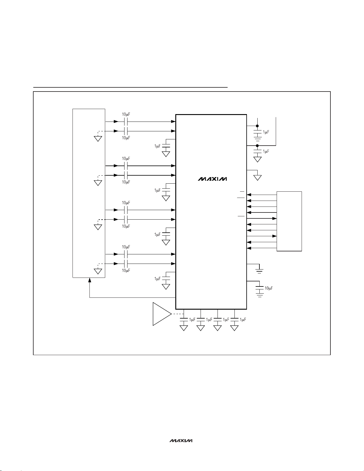
MAX11043
4-Channel, 16-Bit, Simultaneous-Sampling ADCs
with PGA, Filter, and 8-/12-Bit Dual-Stage DAC
Maxim cannot assume responsibility for use of any circuitry other than circuitry entirely embodied in a Maxim product. No circuit patent licenses are
implied. Maxim reserves the right to change the circuitry and specifications without notice at any time.
32
____________________Maxim Integrated Products, 120 San Gabriel Drive, Sunnyvale, CA 94086 408-737-7600
© 2008 Maxim Integrated Products is a registered trademark of Maxim Integrated Products, Inc.
Typical Operating Circuit
*SEE NOTE
RADAR
FRONT END
*SEE NOTE
*SEE NOTE
*SEE NOTE
ECHO+
ECHO-
ECHO+
ECHO-
ECHO+
ECHO-
ECHO+
ECHO-
AINAP
AINAN
REFA
AINBP
AINBN
REFB
AINCP
AINCN
REFC
AINDP
AINDN
REFD
MAX11043
DVDD
AVDD
AGND
CS
UP/DWN
DACSTEP
CONVRUN
EOC
SHDN
SCLK
DOUT
DIN
OSCIN
DGND
DVREG
TO
DIGITAL
SUPPLY
TO
ANALOG
SUPPLY
DSP
AOUT
EXT
REF
*NOTE: CONNECT TO AGND FOR SINGLE-ENDED OPERATION.
REFDACH REFDACLREFDACREFBP
 Loading...