

Page 1

General Description
The MAX11008 controller biases RF LDMOS power
devices found in cellular base stations and other wireless infrastructure equipment. Each controller includes
a high-side current-sense amplifier with programmable
gains of 2, 10, and 25 to monitor the LDMOS drain current over a range of 20mA to 5A. The MAX11008 supports up to two external diode-connected transistors to
monitor the LDMOS temperatures while an internal temperature sensor measures the local die temperature. A
12-bit successive-approximation register (SAR) analogto-digital converter (ADC) converts the analog signals
from the programmable-gain amplifiers (PGAs), external temperature sensors, internal temperature measurement, and two additional auxiliary inputs. The
MAX11008 automatically adjusts the LDMOS bias voltages by applying temperature, AIN, and/or drain current samples to data stored in lookup tables (LUTs).
The MAX11008 includes two gate-drive channels, each
consisting of a 12-bit DAC to generate the positive gate
voltage for biasing the LDMOS devices. Each gatedrive output supplies up to ±2mA of gate current. The
gate-drive amplifier is current-limited to ±25mA and
features a fast clamp to AGND.
The MAX11008 contains 4Kb of on-chip, nonvolatile
EEPROM organized as 256 bits x 16 bits to store LUTs
and register information. The device operates from
either a 4-wire 16MHz SPI™-/MICROWIRE™-compatible or an I2C-compatible serial interface.
The MAX11008 operates from a +4.75V to +5.25V analog supply with a typical supply current of 2mA, and a
+2.7V to +5.25V digital supply with a typical supply of
3mA. The device is packaged in a 48-pin, 7mm x 7mm,
thin QFN package and operates over the extended
(-40°C to +85°C) temperature range.
Applications
Cellular Base Stations
Microwave Radio Links
Feed-Forward Power Amps
Transmitters
Industrial Process Control
Features
♦ On-Chip 4Kb EEPROM for Storing LDMOS Bias
Characteristics
♦ Integrated High-Side Current-Sense PGA with
Gain of 2, 10, or 25
♦ ±0.75% Accuracy for Sense Voltage Between
+75mV and +1250mV
♦ Full-Scale Sense Voltage
+100mV with a Gain of 25
+250mV with a Gain of 10
+1250mV with a Gain of 2
♦ Common-Mode Range, LDMOS Drain Voltage:
+5V to +32V
♦ Adjustable Low-Noise 0 to AV
DD
Output Gate
Bias Voltage Range
♦ Fast Clamp to AGND for LDMOS Protection
♦ 12-Bit DAC Control of Gate with Temperature
♦ Internal Die Temperature Measurement
♦ 2-Channel External Temperature Measurement
through Remote Diodes
♦ Internal 12-Bit ADC Measurement for
Temperature, Current, and Voltage Monitoring
♦ User-Selectable Serial Interface
400kHz/1.7MHz/3.4MHz I
2
C-Compatible Interface
16MHz SPI-/MICROWIRE-Compatible Interface
MAX11008
Dual RF LDMOS Bias Controller with
Nonvolatile Memory
________________________________________________________________
Maxim Integrated Products
1
19-4371; Rev 0; 11/08
For pricing, delivery, and ordering information, please contact Maxim Direct at 1-888-629-4642,
or visit Maxim’s website at www.maxim-ic.com.
EVALUATION KIT
AVAILABLE
SPI is a trademark of Motorola, Inc.
MICROWIRE is a trademark of National Semiconductor Corp.
Ordering Information
+
Denotes a lead-free/RoHS-compliant package.
*
EP = Exposed pad.
Note: The device is specified over the -40°C to +85°C operating
temperature range.
PART PIN-PACKAGE
MAX11008BETM+ 48 TQFN-EP* ±3
TEMP
ERROR (°C)
Page 2

MAX11008
Dual RF LDMOS Bias Controller with
Nonvolatile Memory
2 _______________________________________________________________________________________
ABSOLUTE MAXIMUM RATINGS
ELECTRICAL CHARACTERISTICS
(V
CS_+
= +32V, AVDD= DVDD= +5V ±5%, external V
REFADC
= +2.5V, external V
REFDAC
= +2.5V, C
REF
= 0.1µF, C
GATE_
= 0.1nF,
V
SENSE
= V
CS_+
- V
CS_-
, TA= -40°C to +85°C, unless otherwise noted. Typical values are at TA= +25°C.)
Stresses beyond those listed under “Absolute Maximum Ratings” may cause permanent damage to the device. These are stress ratings only, and functional
operation of the device at these or any other conditions beyond those indicated in the operational sections of the specifications is not implied. Exposure to
absolute maximum rating conditions for extended periods may affect device reliability.
AVDDto AGND .........................................................-0.3V to +6V
DV
DD
to DGND.........................................................-0.3V to +6V
AGND to DGND.....................................................-0.3V to +0.3V
CS_+, CS_- to AGND .............................................-0.3V to +34V
CS_+ to CS_-
If CS_+ > 6V .........................................................-0.3V to +6V
If CS_+ ≤ 6V .......................................................-0.3V to V
CS_-
Analog Inputs/Outputs to AGND ..................................................
...........................-0.3V to the lower of (AV
DD
+ 0.3V) and +6V
Digital Inputs/Outputs to DGND
(except SDA/DIN and SCL/SCLK)............................................
............................-0.3V to the lower of (DV
DD
+ 0.3V) and +6V
SDA/DIN and SCL/SCLK to DGND ..........................-0.3V to +6V
Continuous Input Current (all terminals)...........................±50mA
Continuous Power Dissipation (T
A
= +70°C)
48-Pin, 7mm x 7mm, TQFN (derate 27.8mW/°C above
+70°C).....................................................................2222.2mW
Operating Temperature Range ...........................-40°C to +85°C
Junction Temperature......................................................+150°C
Storage Temperature Range .............................-65°C to +150°C
Lead Temperature (soldering, 10s) .................................+300°C
HIGH-SIDE CURRENT-SENSE PGA
Common-Mode Input Voltage
Range
Common-Mode Rejection Ratio CMRR 5V < V
CS_+ Input Bias Current I
CS_- Input Bias Current I
Minimum Sense Voltage Range
for ±0.75% V
Minimum Sense Voltage Range
for ±2.5% V
Total PGAOUT Voltage Error V
PGAOUT Capacitive Load C
PGAOUT Settling Time t
Saturation Recovery Time
PARAMETER SYMBOL CONDITIONS MIN TYP MAX UNITS
SENSE
SENSE
V
,
CS1+
V
CS2+
CS_+
CS_-
SENSE
Accuracy
Accuracy
PGAOUT
HSCS
CS_+
< 100mV over the common-mode
V
SENSE
range
< 100mV over the common-mode
V
SENSE
range
Gain = 25 0 100
Gain = 10 0 250Full-Scale Sense Voltage Range V
Gain = 2 0 1250
Gain = 25 75 100
Gain = 10 75 250
Gain = 2 75 1250
Gain = 25 20 100
Gain = 10 20 250
Gain = 2 20 1250
= 75mV ±0.1 ±0.75 %
SENSE
(Note 1) < 25 µs
Settles to within ±0.5% accuracy from
V
= 3 x full scale
SENSE
< 32V 110 dB
532V
135 195 µA
< 45 µs
±1 µA
50 pF
mV
mV
mV
Page 3

MAX11008
Dual RF LDMOS Bias Controller with
Nonvolatile Memory
_______________________________________________________________________________________ 3
ELECTRICAL CHARACTERISTICS (continued)
(V
CS_+
= +32V, AVDD= DVDD= +5V ±5%, external V
REFADC
= +2.5V, external V
REFDAC
= +2.5V, C
REF
= 0.1µF, C
GATE_
= 0.1nF,
V
SENSE
= V
CS_+
- V
CS_-
, TA= -40°C to +85°C, unless otherwise noted. Typical values are at TA= +25°C.)
PARAMETER SYMBOL CONDITIONS MIN TYP MAX UNITS
LDMOS GATE DRIVER (Gain = 2)
I
GATE_
Output Gate-Drive Voltage Range V
Output Impedance R
GATE_ Settling Time t
Output Capacitive Load C
GATE_
GATE_
GATE_
GATE_
I
GATE_
Measured at DC 0.1 Ω
R
0.5V to 4.5V (Note 1)
R
R
GATE_ Noise 1kHz to 1MHz 1000 µV
Maximum Power-On Transient ±100 mV
Output Short-Circuit Current Limit I
SC
Total Unadjusted Error TUE
Total Unadjusted Error without
Offset
TUE
NO_OFFSET
1s, sinking or sourcing ±25 mA
Worst case at CODE = 4063, use
external reference (Note 2)
CalCODE = 2457, MaxCODE = 2867,
use external reference, T
(Note 2)
Drift Gain = 2, MaxCODE = 2867 (Note 2) ±15 µV/°C
Clamp to Zero Delay C
Output-Safe Switch OnResistance
R
OPSW
V
MONITOR ADC (DC characteristics)
Resolution N
Differential Nonlinearity DNL
Integral Nonlinearity INL
ADC
ADC
ADC
(Note 5) -2 +2 LSB
Offset Error ±2 ±4 LSB
Gain Error (Note 6) ±2 ±4 LSB
Gain Temperature Coefficient ±0.4 ppm/°C
Offset Temperature Coefficient ±0.4 ppm/°C
MONITOR ADC DYNAMIC CHARACTERISTICS (1kHz sine-wave input, 2.5V
Signal-to-Noise Plus Distortion SINAD 70 dB
Total Harmonic Distortion THD Up to 5th harmonic -82 dBc
Spurious-Free Dynamic Range SFDR 86 dBc
Intermodulation Distortion IMD f
IN1
Full-Power Bandwidth -3dB 1 MHz
Full-Linear Bandwidth SINAD > 68dB 100 kHz
= ±0.1mA 0.1
= ±2mA 0.75
= 500Ω, C
S
= 0Ω 0 0.5
SERIES
= 500Ω 0 15,000
SERIES
GATE_
= 15µF, V
GATE_
=
AV
AV
45 ms
±7 ±25 mV
= +25°C
A
= 0.5nF (Note 3) 1 µs
GATE_
clamped to AGND (Note 4) 300 Ω
GATE_
12 Bits
, up to 94.4ksps)
P-P
= 0.99kHz, f
= 1.02kHz 76 dBc
IN2
-
DD
0.1
-
DD
0.75
±8 mV
±2 LSB
V
nF
P-P
Page 4

MAX11008
Dual RF LDMOS Bias Controller with
Nonvolatile Memory
4 _______________________________________________________________________________________
ELECTRICAL CHARACTERISTICS (continued)
(V
CS_+
= +32V, AVDD= DVDD= +5V ±5%, external V
REFADC
= +2.5V, external V
REFDAC
= +2.5V, C
REF
= 0.1µF, C
GATE_
= 0.1nF,
V
SENSE
= V
CS_+
- V
CS_-
, TA= -40°C to +85°C, unless otherwise noted. Typical values are at TA= +25°C.)
PARAMETER SYMBOL CONDITIONS MIN TYP MAX UNITS
MONITOR ADC CONVERSION RATE
Power-Up Time (External
Reference)
Power-Up Time (Internal
Reference)
Acquisition Time t
Conversion Time t
Aperture Delay t
t
PUEXT
t
PUINT
ACQ
CONV
AD
Internally clocked, T
MONITOR ADC ANALOG INPUT (ADCIN1, ADCIN2)
Input Voltage Range V
ADCIN
Relative to AGND (Note 7) 0 V
Input Leakage Current VIN = 0 and VIN = V
Input Capacitance C
ADCIN
TEMPERATURE MEASUREMENTS
Internal Sensor Measurement
Error
External Sensor Measurement
Error (Note 9)
TA = +25°C ±0.25
T
= T
A
TA = +25°C ±1
= T
T
A
Relative Temperature Accuracy TA = T
Temperature Resolution 1/8 °C/LSB
E xter nal D i od e D r i ve C ur r ent ( Low ) 3.25 4 µA
E xter nal D i od e D r i ve C ur r ent ( H i g h) 68 75 µA
INTERNAL REFERENCE
REFADC/REFDAC Output
Voltage
REFADC/REFDAC Temperature
Coefficient
V
REFADC
V
REFDAC
TC
REFADC
TC
REFDAC
,
TA = +25°C 2.49 2.50 2.51 V
,
REFADC/REFDAC Output
Impedance
Capacitive Bypass at
REFADC/REFDAC
Power-Supply Rejection Ratio PSRR AVDD = 5V ± 5% 64 dB
EXTERNAL REFERENCE
REFADC Input Voltage Range V
REFADC Input Current I
REFDAC Input Voltage Range V
REFADC
REFADC
REFDAC
V
REFADC
Acquisition/between conversions ±0.01
REFDAC Input Current S tati c cur r ent w hen the D AC i s not cal i b r ated 0.1 µA
to T
MIN
MAX
to T
MIN
MAX
to T
MIN
MAX
= 2.5V, f
1.1 µs
70 µs
0.5 µs
= +25°C 10 µs
A
20 ns
REFADC
AV
DD
±0.01 µA
34 pF
(Note 8) ±1.5 ±3
±3
(Note 9) ±0.4 °C
±15 ppm/°C
6.5 kΩ
270 pF
1.0 AV
= 100ksps 60 80
SAMPLE
0.7 2.5 V
DD
V
°C
°C
V
µA
Page 5

MAX11008
Dual RF LDMOS Bias Controller with
Nonvolatile Memory
_______________________________________________________________________________________ 5
ELECTRICAL CHARACTERISTICS (continued)
(V
CS_+
= +32V, AVDD= DVDD= +5V ±5%, external V
REFADC
= +2.5V, external V
REFDAC
= +2.5V, C
REF
= 0.1µF, C
GATE_
= 0.1nF,
V
SENSE
= V
CS_+
- V
CS_-
, TA= -40°C to +85°C, unless otherwise noted. Typical values are at TA= +25°C.)
GATE-DRIVER DAC DC ACCURACY
Resolution N
Integral Nonlinearity INL
Differential Nonlinearity DNL
DIGITAL INPUTS (SCL/SCLK, SDA/DIN, A0/CS, A1/DOUT, A2/N.C., CNVST, OPSAFE1, OPSAFE2)
Input High Voltage V
Input Low Voltage V
Input Hysteresis V
Input Leakage Current Digital inputs at 0 or V
Input Capacitance C
DIGITAL OUTPUTS (SDA/DIN, ALARM, BUSY, DOUT)
Output High Voltage V
Output Low Voltage V
Three-State Leakage I
Three-State Capacitance 5pF
POWER SUPPLIES (Note 12)
PARAMETER SYMBOL CONDITIONS MIN TYP MAX UNITS
DAC
DAC
DAC
IH
IL
HYS
IN
OH
OL
IL
Measured at GATE_ ±2 ±4 LSB
Guaranteed monotonic (Note 10) ±1 LSB
SDA/DIN and SCL/SCLK only
A0/CS, A1/DOUT, A2/N.C., CNVST,
OPSAFE1, OPSAFE2 only
SDA/DIN and SCL/SCLK only
A0/CS, A1/DOUT, A2/N.C., CNVST,
OPSAFE1, OPSAFE2 only
SDA/DIN and SCL/SCLK only
ALARM and BUSY only, I
SDA/DIN and A1/DOUT, I
(Note 11)
ALARM and BUSY only, I
Digital inputs at 0 or DV
DVDD
SOURCE
= 3mA,
SINK
= 0.3mA 0.3
SINK
DD
= 0.2mA
0.7 x
DV
2.3
0.08 x
DV
DV
- 0.4V
12 Bits
DD
DD
±0.1 ±1 µA
5pF
DD
±0.1 ±1 µA
0.3 x
DV
0.7
0.4
DD
V
V
V
V
V
Analog Supply Voltage Range AV
Digital Supply Voltage Range DV
Analog Supply Current I
Digital Supply Current I
AVDD
DVDD
DD
DD
AVDD = 5V 2 4 mA
Shutdown (Note 13) 0.4 2 µA
DVDD = 5V 3 6 mA
Shutdown 2 32 µA
4.75 5.25 V
2.7
AV
+ 0.3
DD
V
Page 6

MAX11008
Dual RF LDMOS Bias Controller with
Nonvolatile Memory
6 _______________________________________________________________________________________
SPI TIMING CHARACTERISTICS (Notes 14, 15, Figure 1)
(DVDD= +2.7V to +5.25V, AVDD= +4.75V to +5.25V, V
DGND
= V
AGND
= 0, external V
REFADC
= +2.5V, external V
REFDAC
= +2.5V,
C
REF
= 0.1µF, TA= -40°C to +85°C, unless otherwise noted.)
I2C SLOW-/FAST-MODE TIMING CHARACTERISTICS (Notes 14, 15, Figure 4)
(DVDD= +2.7V to +5.25V, AVDD= +4.75V to +5.25V, V
DGND
= V
AGND
= 0, external V
REFADC
= +2.5V, external V
REFDAC
= +2.5V,
C
REF
= 0.1µF, TA= -40°C to +85°C, unless otherwise noted.)
PARAMETER SYMBOL CONDITIONS MIN TYP MAX UNITS
SCLK Clock Period t
SCLK High Time t
SCLK Low Time t
DIN to SCLK Rise Setup Time t
DIN to SCLK Rise Hold Time t
SCLK Fall to DOUT Transition t
CS Fall to DOUT Enable t
CS Rise to DOUT Disable t
CS Rise or Fall to SCLK Rise t
CS Pulse-Width High t
Last SCLK Rise to CS Rise t
CP
CH
CL
DS
DH
DO
DV
TR
CSS
CSW
CSH
CL = 30pF 20 ns
CL = 30pF 50 ns
CL = 30pF (Note 16) 50 ns
SCL Clock Frequency f
Bus Free Time Between a STOP
and START Condition
Hold Time (Repeated) for START
Condition
Setup Time for a Repeated
START Condition
SCL Pulse-Width Low t
SCL Pulse-Width High t
Data Setup Time t
Data Hold Time t
SDA, SCL Rise Time t
SDA, SCL Fall Time t
SDA Fall Time t
Setup Time for STOP Condition t
Capacitive Load for Each Bus
Line
Pulse Width of Spikes
Suppressed by the Input Filter
PARAMETER SYMBOL CONDITIONS MIN TYP MAX UNITS
SCL
t
BUF
t
HD:STA
t
SU:STA
LOW
HIGH
SU:DAT
HD:DAT
SU:STO
C
t
SP
After this period, the first clock pulse is
generated
(Note 17) 0.004 0.9 µs
Receiving (Note 18) 0 300 ns
R
Receiving (Note 18) 0 300 ns
F
Transmitting (Notes 18, 19)
F
(Note 20) 400 pF
B
(Note 21) 50 ns
62.5 ns
25 ns
25 ns
15 ns
0ns
12.5 ns
50 ns
0ns
0 400 kHz
1.3 µs
0.6 µs
0.6 µs
1.3 µs
0.6 µs
100 ns
20 + 0.1
x C
B
0.6 µs
250 ns
Page 7

MAX11008
Dual RF LDMOS Bias Controller with
Nonvolatile Memory
_______________________________________________________________________________________ 7
I2C HIGH-SPEED-MODE TIMING CHARACTERISTICS (Notes 14, 15, Figure 4)
(DVDD= +2.7V to +5.25V, AVDD= +4.75V to +5.25V, V
DGND
= V
AGND
= 0, external V
REFADC
= +2.5V, external V
REFDAC
= +2.5V,
C
REF
= 0.1µF, TA= -40°C to +85°C, unless otherwise noted.)
MISCELLANEOUS TIMING CHARACTERISTICS (Note 15)
(DVDD= +2.7V to +5.25V, AVDD= +4.75V to +5.25V, V
DGND
= V
AGND
= 0, external V
REFADC
= +2.5V, external V
REFDAC
= +2.5V,
C
REF
= 0.1µF, TA= -40°C to +85°C, unless otherwise noted.)
PARAMETER SYMBOL CONDITIONS
Serial Clock Frequency f
Setup Time (Repeated) START
Condition
Hold Time (Repeated) START
Condition
SCL Pulse-Width Low t
SCL Pulse-Width High t
Data Setup Time t
Data Hold Time t
SCL Rise Time t
SCL Rise Time t
SCL Fall Time t
SDA Rise Time t
SDA Fall Time t
Setup Time for STOP Condition t
Capacitive Load for Each Bus Line C
Pulse Width of Spikes Suppressed
by the Input Filter
SCL
t
SU:STA
t
HD:STA
LOW
HIGH
SU:DAT
HD:DAT
RCL
RCL1
FCL
RDA
FDA
SU:STO
B
t
SP
(Note 17) 4 70 4 150 ns
After a repeated START
condition and after an
acknowledge bit
(Note 20) 100 400 ns
(Note 21) 0 10 0 10 ns
CB = 100pF max CB = 400pF
MIN MAX MIN MAX
0 3.4 0 1.7 MHz
160 160 ns
160 160 ns
160 320 ns
80 120 ns
10 10 ns
10 40 20 80 ns
10 80 20 160 ns
10 40 20 80 ns
10 80 20 160 ns
10 80 20 160 ns
160 160 ns
UNITS
Minimum Time to Wait After a Write
Command Before Reading Back
Data from the Same Location
CNVST Active-Low Pulse Width in
ADC Clock Mode 01
CNVST Active-Low Pulse Width in
ADC Clock Mode 11 to Initiate a
Temperature Conversion
CNVST Active-Low Pulse Width in
ADC Clock Mode 11 for ADCIN1/2
Acquisition
ADC Power-Up Time (External
Reference)
ADC Power-Up Time (Internal
Reference)
PARAMETER SYMBOL CONDITIONS MIN TYP MAX UNITS
t
RDBK
t
CNV01
t
CNV11
t
ACQ11A
t
APUEXT
t
APUINT
(Note 22) 1 µs
20 ns
20 ns
1.5 µs
1.1 µs
70 µs
Page 8

MAX11008
Dual RF LDMOS Bias Controller with
Nonvolatile Memory
8 _______________________________________________________________________________________
MISCELLANEOUS TIMING CHARACTERISTICS (Note 15) (continued)
(DVDD= +2.7V to +5.25V, AVDD= +4.75V to +5.25V, V
DGND
= V
AGND
= 0, external V
REFADC
= +2.5V, external V
REFDAC
= +2.5V,
C
REF
= 0.1µF, TA= -40°C to +85°C, unless otherwise noted.)
Note 1: Output settles to within ±0.5% of final value.
Note 2: Total unadjusted errors are for the entire gate-drive channel including the 12-bit DAC, and the gate driver is measured at
the GATE1 and GATE2 outputs.
Note 3: V
GATE_
= VDD- 0.1. Measured from when OPSAFE1 or OPSAFE2 is set high.
Note 4: During power-on-reset, the output safe switch is closed. The output safe switch is opened under user software control.
Note 5: Guaranteed to be 11 bits linearly accurate.
Note 6: Offset nulled.
Note 7: The absolute range for analog inputs is from 0 to V
AVDD
.
Note 8: Internal temperature-sensor performance is guaranteed by design.
Note 9: The MAX11008 and the external sensor are at the same ambient temperature. External sensor measurement error is tested
with a diode-connected 2N3904.
Note 10: Guaranteed monotonicity. Accuracy is degraded at lower V
REFDAC
.
Note 11: SDA/DIN is an open-drain output only when in I
2
C mode. A1/DOUT is an open-drain output only when in SPI mode.
Note 12: Supply-current limits are valid only when digital inputs are set to DGND or supply voltage. Timing specifications are only
guaranteed when inputs are driven rail-to-rail.
Note 13: Shutdown supply currents are typically 0.4µA for AV
DD
; maximum specification is limited by automated test equipment.
Note 14: All times are referred to the 50% point between V
IH
and VILlevels.
Note 15: Guaranteed by design. Not production tested.
Note 16: DOUT will go into three-state mode after the CS rising edge. Keep CS low long enough for the DOUT value to be sampled
before it goes to three-state.
Note 17: A master device must provide a hold time of at least 300ns for the SDA signal (referred to V
IL
of the SCL signal) to bridge
the undefined region of SCL’s falling edge.
Note 18: t
R
and tFmeasured between 0.3 x DVDDand 0.7 x DVDD.
Note 19: C
B
= total capacitance of one bus line in pF. For bus loads between 100pF and 400pF, the timing parameters should be
linearly interpolated.
Note 20: An appropriate bus pullup resistance must be selected depending on board capacitance.
Note 21: Input filters on the SDA and SCL inputs suppress noise spikes less than 50ns.
Note 22: When a command is written to the serial interface, the command is passed by the internal oscillator clock and executed.
There is a small synchronization delay before the new value is written to the appropriate register. If the serial interface
attempts to read the new value back before t
RDBK
, the new data is not corrupted; however, the result of the read command
may not reflect the new value.
Note 23: This is the minimum time from the end of a command before CNVST should be asserted. The time allows for the data from
the preceding write to arrive and set up the chip in preparation for the CNVST. The time need only be observed when the
write affects the ADC controls. Failure to observe this time may lead to incorrect conversions (for example, conversion of
the wrong ADC channel).
PARAMETER SYMBOL CONDITIONS MIN TYP MAX UNITS
DAC Power-Up Time (External
Reference)
DAC Power-Up Time (Internal
Reference)
Acquisition Time (Internally Timed
in ADC Clock Modes 00 or 01)
Conversion Time (Internally
Clocked)
Delay to Start of Conversion Time t
Temperature Conversion Time
(Internally Clocked)
t
DPUEXT
t
DPUINT
t
ACQ
t
CONV
CONVW
t
CONVT
Internally clocked, TA = +25°C 10 µs
(Note 23) 1.3 µs
2µs
70 µs
70 µs
0.6 µs
Page 9
MAX11008
Dual RF LDMOS Bias Controller with
Nonvolatile Memory
_______________________________________________________________________________________ 9
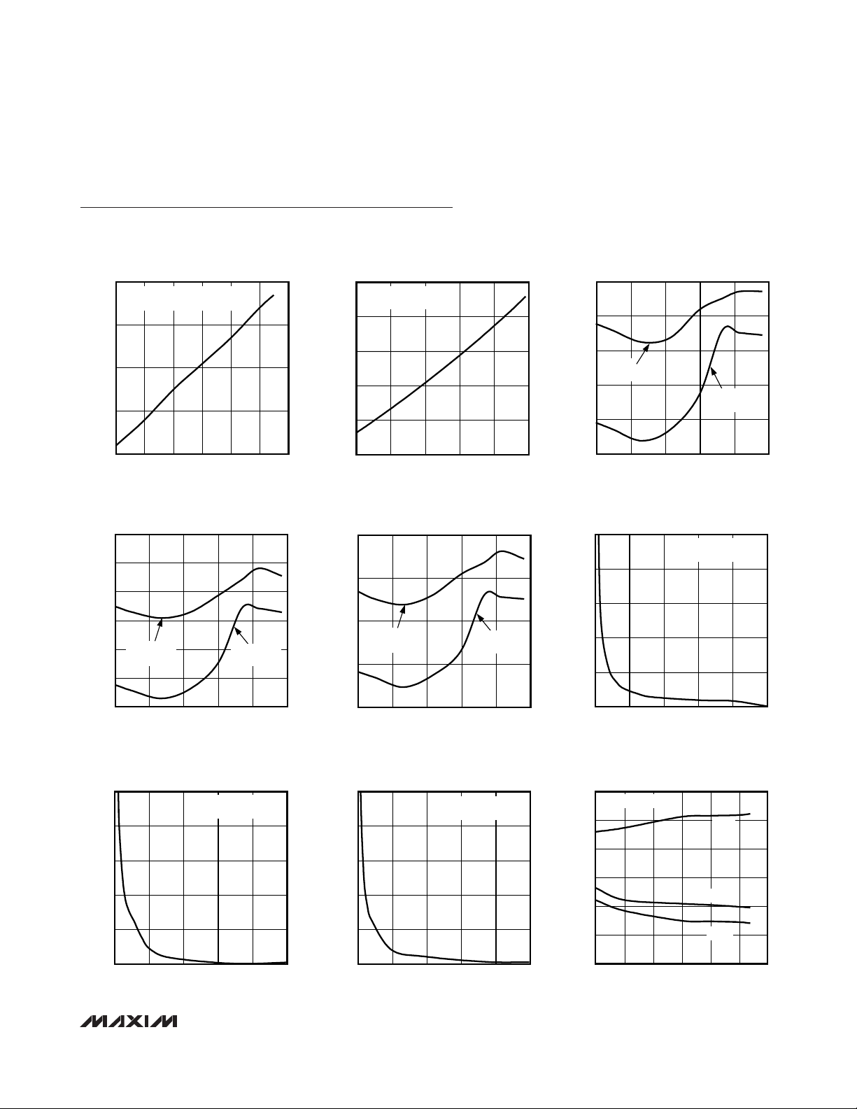
Typical Operating Characteristics
(AVDD= DVDD= 5V, external V
REFADC
= 2.5V, external V
REFDAC
= 2.5V, V
CS_-
= V
CS_+
= 32V, C
REF
= 0.1µF, TA= +25°C, unless oth-
erwise noted.)
2.06
2.07
2.08
2.09
2.10
4.7 4.94.8 5.0 5.1 5.2 5.3
ANALOG SUPPLY CURRENT
vs. SUPPLY VOLTAGE
MAX11008 toc01
AVDD (V)
I
AVDD
(mA)
DVDD = 5V
INT REF AND DACS TURNED ON
1.0
1.5
2.5
2.0
3.0
3.5
2.70 3.743.22 4.26 4.78 5.30
DIGITAL SUPPLY CURRENT
vs. SUPPLY VOLTAGE
MAX11008 toc02
DVDD (V)
I
DVDD
(mA)
AVDD = 5V
WD OSC TURNED ON
-0.8
-0.6
-0.2
-0.4
0
0.2
-40 20-10 50 80 110
CURRENT-SENSE AMPLIFIER OUTPUT
ERROR vs. TEMPERATURE (G = 2)
MAX11008 toc03
TEMPERATURE (°C)
PGAOUT_ ERROR (%)
AFTER
CALIBRATION
BEFORE
CALIBRATION
-0.8
-0.4
-0.6
0
-0.2
0.2
0.4
-40 20-10 50 80 110
CURRENT-SENSE AMPLIFIER OUTPUT
ERROR vs. TEMPERATURE (G = 10)
MAX11008 toc04
TEMPERATURE (°C)
PGAOUT_ ERROR (%)
AFTER
CALIBRATION
BEFORE
CALIBRATION
CURRENT-SENSE AMPLIFIER OUTPUT
ERROR vs. TEMPERATURE (G = 25)
MAX11008 toc05
TEMPERATURE (°C)
PGAOUT_ ERROR (%)
805020-10
-0.6
-0.3
0
0.3
-0.9
-40 110
AFTER
CALIBRATION
BEFORE
CALIBRATION
0
0.2
0.6
0.4
0.8
1.0
0500250 750 1000 1250
CURRENT-SENSE AMPLIFIER OUTPUT
ERROR vs. SENSE VOLTAGE (G = 2)
MAX11008 toc06
V
SENSE
(mV)
OUTPUT ERROR (%)
OUTPUT AT PGAOUT_
CMV = 32V
0
0.2
0.6
0.4
0.8
1.0
0 10050 150 200 250
CURRENT-SENSE AMPLIFIER OUTPUT
ERROR vs. SENSE VOLTAGE (G = 10)
MAX11008 toc07
V
SENSE
(mV)
OUTPUT ERROR (%)
OUTPUT AT PGAOUT_
CMV = 32V
0
1
3
2
4
5
04020 60 80 100
CURRENT-SENSE AMPLIFIER OUTPUT
ERROR vs. SENSE VOLTAGE (G = 25)
MAX11008 toc08
V
SENSE
(mV)
OUTPUT ERROR (%)
OUTPUT AT PGAOUT_
CMV = 32V
0
0.10
0.05
0.20
0.15
0.25
0.30
5152010 25 30 35
CURRENT-SENSE AMPLIFIER
OUTPUT ERROR vs. CMV
MAX11008 toc09
COMMON-MODE VOLTAGE (V)
OUTPUT ERROR (%)
V
SENSE
= 75mV
G = 2
G = 25
G = 10
Page 10
MAX11008
Dual RF LDMOS Bias Controller with
Nonvolatile Memory
10 ______________________________________________________________________________________
Typical Operating Characteristics (continued)
(AVDD= DVDD= 5V, external V
REFADC
= 2.5V, external V
REFDAC
= 2.5V, V
CS_-
= V
CS_+
= 32V, C
REF
= 0.1µF, TA= +25°C, unless oth-
erwise noted.)
2µs/div
CURRENT-SENSE TRANSIENT
RESPONSE (G = 2)
V
SENSE1
1V/div
V
PGAOUT1
1V/div
MAX11008 toc10
0V
0V
1µs/div
CURRENT-SENSE TRANSIENT
RESPONSE (G = 10)
V
SENSE1
200mV/div
V
PGAOUT1
1V/div
MAX11008 toc11
0V
0V
1µs/div
CURRENT-SENSE TRANSIENT
RESPONSE (G = 25)
V
SENSE1
100mV/div
V
PGAOUT1
1V/div
MAX11008 toc12
0V
0V
-4.50
-4.35
-4.05
-4.20
-3.90
-3.75
-40 18-11 47 76 105
GATE VOLTAGE TOTAL UNADJUSTED
ERROR vs. TEMPERATURE
MAX11008 toc13
TEMPERATURE (°C)
V
GATE_
ERROR (mV)
1µs/div
GATE POWER-UP TIME
V
SCL
5V/div
V
SDA
5V/div
V
GATE1
1V/div
MAX11008 toc14
0V
0
0.5
1.5
1.0
2.0
2.5
0200100 300 400 500
GATE_ SETTLING TIME vs. C
GATE
MAX11008 toc16
C
GATE_
(pF)
GATE_ SETTLING TIME (µs)
RS = 500Ω
50% OF SDA STOP EDGE TO
0.5% OF FINAL V
GATE_
4V TRANS ON GATE_ (IODAC_)
10µs/div
MAJOR CARRY TRANSITION GLITCH
V
GATE_
1mV/div
MAX11008 toc17
CODE 7FF TO 800
C
GATE_
= 100pF
-1.0
-0.4
-0.6
-0.8
-0.2
0
0.2
0.4
0.6
0.8
1.0
0 1024 2048 3072 4096
DAC INTEGRAL NONLINEARITY
vs. INPUT CODE
MAX11008 toc18
INPUT CODE
INL (LSB)
-1.0
-0.4
-0.6
-0.8
-0.2
0
0.2
0.4
0.6
0.8
1.0
0 1024 2048 3072 4096
DAC DIFFERENTIAL NONLINEARITY
vs. INPUT CODE
MAX11008 toc19
INPUT CODE
DNL (LSB)
Page 11
MAX11008
Dual RF LDMOS Bias Controller with
Nonvolatile Memory
______________________________________________________________________________________
11
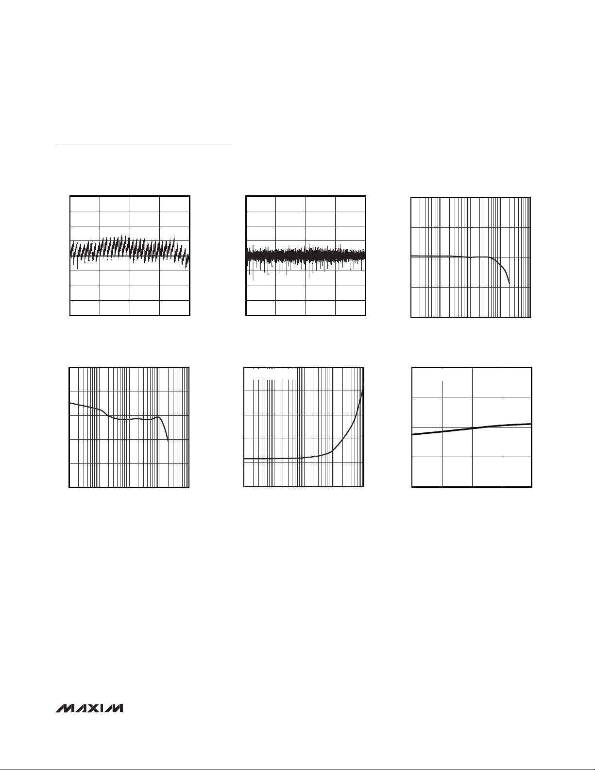
Typical Operating Characteristics (continued)
(AVDD= DVDD= 5V, external V
REFADC
= 2.5V, external V
REFDAC
= 2.5V, V
CS_-
= V
CS_+
= 32V, C
REF
= 0.1µF, TA= +25°C, unless oth-
erwise noted.)
ADC INTEGRAL NONLINEARITY
vs. OUTPUT CODE
1.00
0.75
0.50
0.25
0
ADC INL (LSB)
-0.25
-0.50
-0.75
-1.00
0 1024 2048 3072 4096
OUTPUT CODE
ADC SFDR vs. FREQUENCY
100
90
80
SFDR (dB)
70
60
1.00
MAX11008 toc20
MAX11008 toc23
0.75
0.50
0.25
0
ADC DNL (LSB)
-0.25
-0.50
-0.75
-1.00
0 1024 2048 3072 4096
8
AVDD = DVDD = 5V
7
6
5
SUPPLY CURRENT (mA)
DD
DV
4
ADC DIFFERENTIAL NONLINEARITY
vs. OUTPUT CODE
OUTPUT CODE
DIGITAL SUPPLY CURRENT
vs. SAMPLING RATE
MAX11008 toc21
80
75
70
SINAD (dB)
65
60
0.1 101 100 1000
ADC INTERNAL REFERENCE VOLTAGE
2.5026
MAX11008 toc24
2.5024
2.5022
2.5020
ADC REFERENCE VOLTAGE (V)
ADC SINAD vs. FREQUENCY
FREQUENCY (kHz)
vs. SUPPLY VOLTAGE
AVDD = DV
DD
MAX11008 toc22
MAX11008 toc25
50
0.1 101 100 1000
FREQUENCY (kHz)
3
0.1 101 100 1000
SAMPLING RATE (ksps)
2.5018
4.750 5.0004.875 5.125 5.250
SUPPLY VOLTAGE (V)
Page 12
MAX11008
Dual RF LDMOS Bias Controller with
Nonvolatile Memory
12 ______________________________________________________________________________________
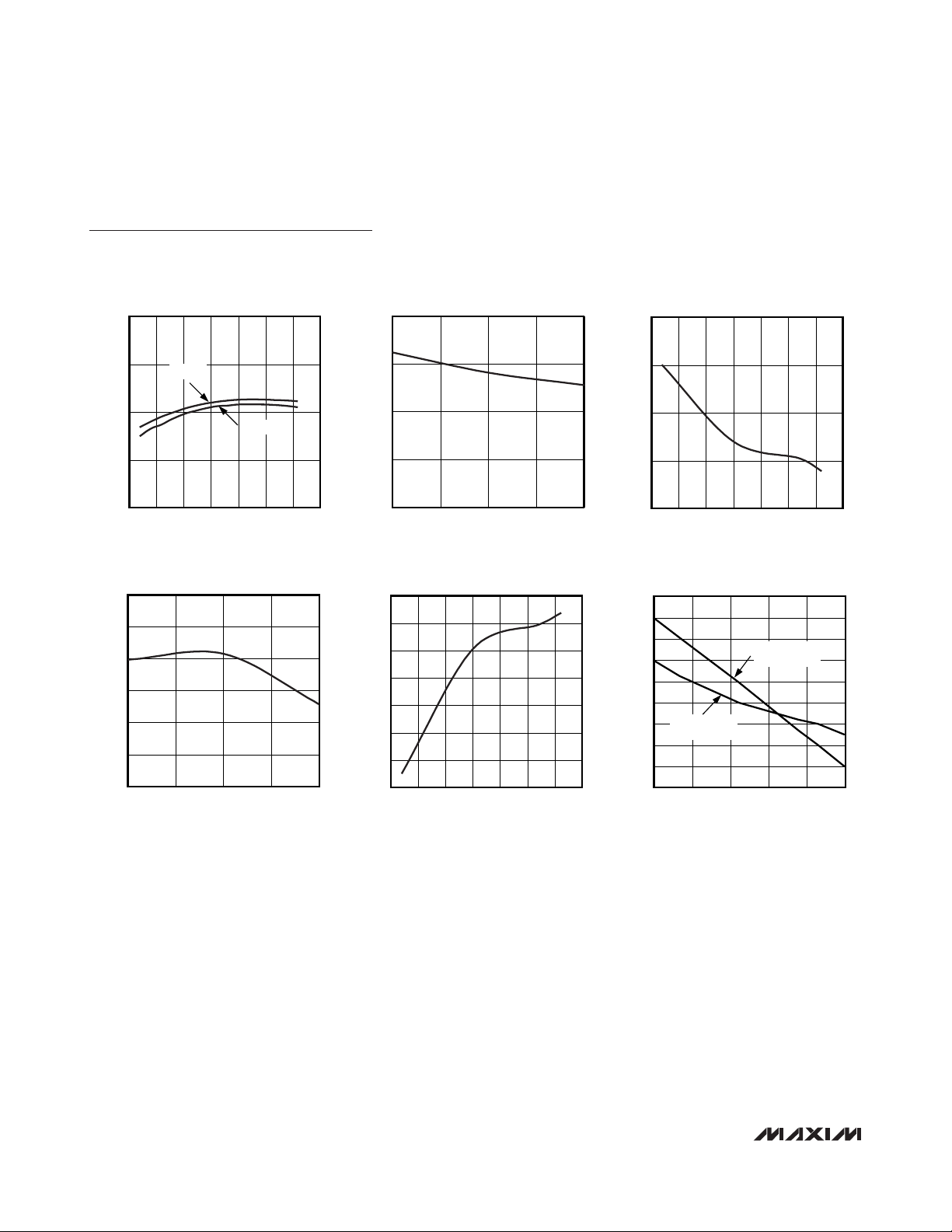
Typical Operating Characteristics (continued)
(AVDD= DVDD= 5V, external V
REFADC
= 2.5V, external V
REFDAC
= 2.5V, V
CS_-
= V
CS_+
= 32V, C
REF
= 0.1µF, TA= +25°C, unless oth-
erwise noted.)
INTERNAL REFERENCE VOLTAGE
vs. TEMPERATURE
2.52
2.0
ADC OFFSET ERROR
vs. ANALOG SUPPLY VOLTAGE
ADC OFFSET ERROR vs. TEMPERATURE
4
2.51
V
REFADC
2.50
REFERENCE VOLTAGE (V)
2.49
2.48
-50 25 50-25 0 75 100 125
TEMPERATURE (°C)
ADC GAIN ERROR
vs. ANALOG SUPPLY VOLTAGE
3.0
2.5
2.0
1.5
1.0
ADC GAIN ERROR (LSB)
0.5
0
4.750 5.0004.875 5.125 5.250
AVDD (V)
V
REFDAC
MAX11008 toc26
1.5
1.0
ADC OFFSET ERROR (LSB)
0.5
0
4.750 5.0004.875 5.125 5.250
4
MAX11008 toc29
3
2
1
0
ADC GAIN ERROR (LSB)
-1
-2
-3
-50 0 25-25 50 75 100 125
AVDD (V)
ADC GAIN EROR vs. TEMPERATURE
TEMPERATURE (°C)
MAX11008 toc27
3
2
ADC OFFSET ERROR (LSB)
1
0
-50 25 50-25 0 75 100 125
0.8
0.6
MAX11008 toc30
0.4
0.2
0
-0.2
EXTERNAL TEMP
-0.4
SENSOR
-0.6
RELATIVE TEMPERATURE ERROR
-0.8
-1.0
-40 18-11 47 76 105
TEMPERATURE (°C)
RELATIVE TEMPERATURE
ERROR vs. TEMPERATURE
INTERNAL TEMP
SENSOR
TEMPERATURE (°C)
MAX11008 toc28
MAX11008 toc31
Page 13

MAX11008
Dual RF LDMOS Bias Controller with
Nonvolatile Memory
______________________________________________________________________________________ 13
______________________________________________________________________________________
13
Pin Description
PIN NAME FUNCTION
1, 31 DGND Digital Ground. Connect both DGND inputs to the same potential.
2 OPSAFE1
3 A0/CS
4 CNVST
5 SPI/I2C Interface-Select Input. Connect to DGND for I2C interface. Connect to DVDD for SPI interface.
6 ALARM Alarm Output
7 OPSAFE2
8 REFDAC DAC Reference Input/Output
9 REFADC ADC Reference Input/Output
10 DXP1 Temperature Diode Positive Input 1. Connect DXP1 to the anode of the external diode.
11 DXN1 Temperature Diode Negative Input 1. Connect DXN1 to the cathode of the external diode.
12 DXP2 Temperature Diode Positive Input 2. Connect DXP2 to the anode of the external diode.
13 DXN2 Temperature Diode Negative Input 2. Connect DXN2 to the cathode of the external diode.
14 ADCIN1 ADC Auxiliary Input 1
15 ADCIN2 ADC Auxiliary Input 2
16 PGAOUT2 Programmable-Gain Amplifier Output 2
17 GATE2 Gate-Drive Amplifier Output 2
18 GATE1 Gate-Drive Amplifier Output 1
19, 25, 30,
34–39, 42, 48
20, 24 AV
21, 22, 23 AGND Analog Ground. Connect all AGND inputs to the same potential.
26 CS2+ C ur r ent- S ense P osi ti ve Inp ut 2. C S 2+ i s the exter nal sense- r esi stor connecti on to the LD M OS 2 sup p l y.
27 CS2- Current-Sense Negative Input 2. CS2- is the external sense-resistor connection to the LDMOS 2 drain.
28 CS1- Current-Sense Negative Input 1. CS1- is the external sense-resistor connection to the LDMOS 1 drain.
29 CS1+ C ur r ent- S ense P osi ti ve Inp ut 1. C S 1+ i s the exter nal sense- r esi stor connecti on to the LD M OS 1 sup p l y.
32, 33, 47 DV
40 PGAOUT1 Programmable-Gain Amplifier Output 1
41 A2/N.C.
43 SCL/SCLK Serial-Clock Input. SCL is the I2C-compatible clock input. SCLK is the SPI-compatible clock input.
44 SDA/DIN S er i al - D ata Inp ut/Outp ut. S D A i s the I2C- com p ati b l e i np ut/outp ut. D IN i s the S P I- com p ati b l e d ata i np ut.
45 A1/DOUT
46 BUSY Busy Output. BUSY goes high to indicate activity.
— EP Exposed Pad. Connect EP to AGND. Internally connected to AGND.
N.C. No Connection. Not internally connected. Leave unconnected.
Output Safe Switch Logic Input 1. Drive OPSAFE1 high to close the output safe switch and clamp
GATE1 to AGND. Drive OPSAFE1 low to open the switch.
Address-Select Input 0/Chip-Select Input. In I
1. In SPI mode, this is the chip-select input.
Active-Low Conversion Start Input. Drive CNVST low to begin a conversion when in clock modes 01
and 11.
Output Safe Switch Logic Input 2. Drive OPSAFE2 high to close the output safe switch and clamp
GATE2 to AGND. Drive OPSAFE2 low to open the switch.
Analog-Supply Input. Connect both AVDD inputs to the same potential.
DD
Digital-Supply Input. Connect all DVDD inputs to the same potential. Connect a 0.1µF capacitor to
DD
.
DV
DD
Address-Select Input 2/N.C. In I
mode, this is a no connection pin.
Address-Select Input 1/Data Out. In I
mode, this is the serial-data output. Data is clocked out on the falling edge of SCLK. DOUT is a highimpedance output when CS is driven high.
2
C mode, this pin is the address-select input 2. See Table 1. In SPI
2
2
C mode, this is the address-select input 0. See Table
C mode, this is the address-select input 1. See Table 1. In SPI
Page 14
MAX11008
Dual RF LDMOS Bias Controller with
Nonvolatile Memory
14 ______________________________________________________________________________________14 ______________________________________________________________________________________
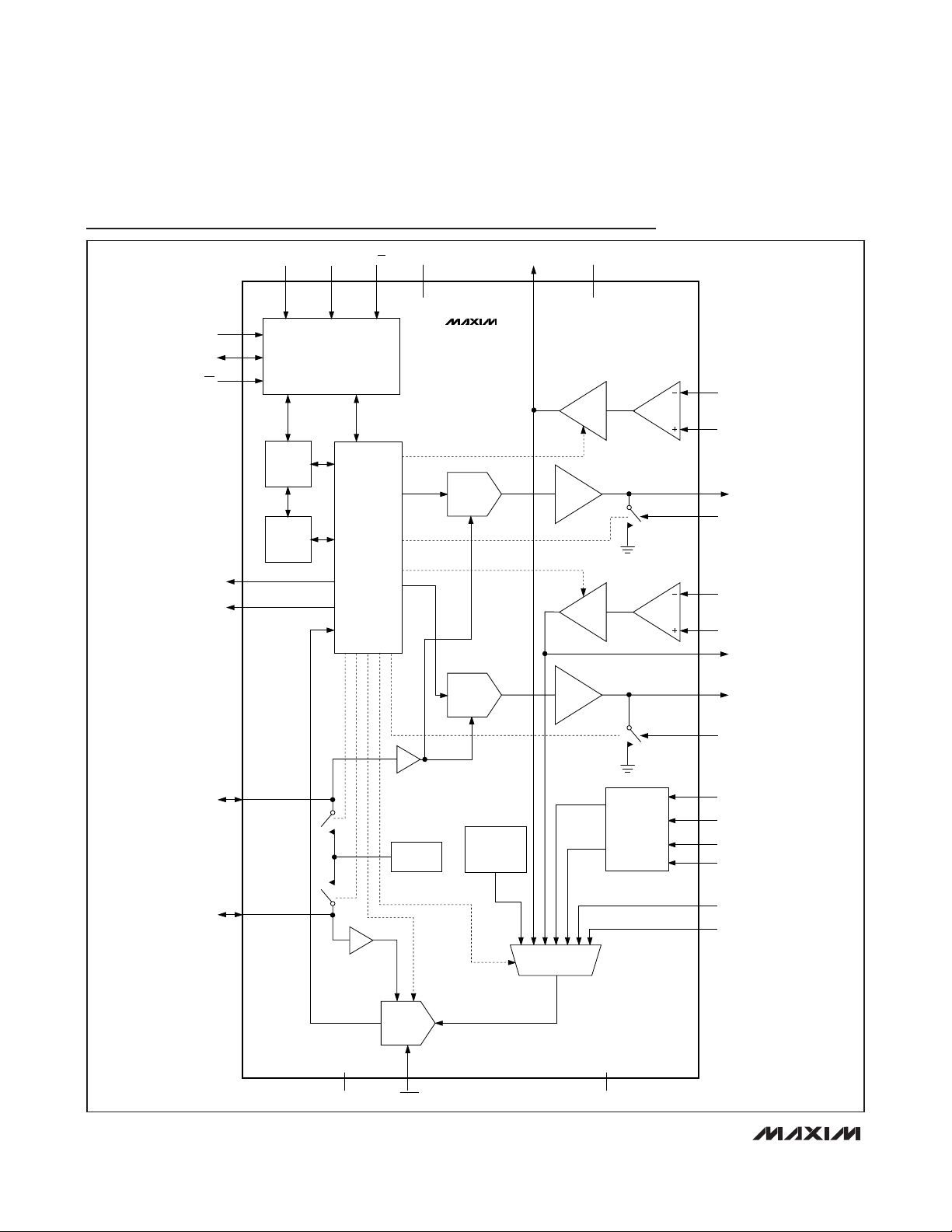
Functional Diagram
A1/DOUTA2/N.C.
A0/CS
DV
DD
PGAOUT1
AV
DD
SCL/SCLK
SDA/DIN
SPI/I2C
ALARM
BUSY
FIFO
EEPROM
SERIAL INTERFACE
REGISTER MAP
AND DIGITAL
CONTROL
MAX11008
12-BIT DAC1
12-BIT DAC 2
CS1+
PGA 1
CS1-
= 2
A
V
PGA 2
= 2
A
V
GATE1
OPSAFE1
CS2+
CS2-
PGAOUT2
GATE2
OPSAFE2
REFDAC
REFADC
2.5V
REFERENCE
12-BIT ADC
CNVST
INTERNAL
TEMPERATURE
SENSOR
MUX
AGNDDGND
EXTERNAL
TEMPERATURE
SENSOR
PROCESSING
DXP1
DXN1
DXP2
DXN2
ADCIN1
ADCIN2
Page 15
MAX11008
Dual RF LDMOS Bias Controller with
Nonvolatile Memory
______________________________________________________________________________________ 15______________________________________________________________________________________ 15
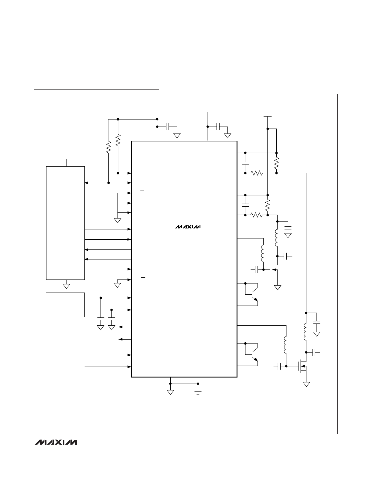
Typical Application Circuits—I2C Interface
DV
DD
0.1µF
4.7kΩ
DV
4.7kΩ
5V
SCL/SCLK
SDA/DIN
A0/CS
A1/DOUT
A2/N.C.
µC
OPSAFE1
OPSAFE2
ALARM
BUSY
CNVST
SPI/I2C
DD
MAX11008
AV
DD
0.1µF
AV
DD
CS1+
CS1-
CS2+
CS2-
GATE2
RF IN
DXP2
32V
*
C
F
R
*
F
*
C
F
*
R
F
R
SENSE
R
SENSE
LDMOS 1
RF OUT
EXTERNAL
2.5V
REFERENCE
REFADC
DXN2
GATE1
DXP1
DXN1
I2C SERIAL INTERFACE
= 1/(2 π RFCF).
CUTOFF
SECTION.
RF IN
RF OUT
LDMOS 2
0.1µF 0.1µF
*SDA RESISTOR VALUE VARIES WITH LOAD AND SCL FREQUENCY. SEE THE
*SELECT RF AND CF BASED ON DESIRED FILTER CUTOFF FREQUENCY WHERE f
LIMIT R
REFDAC
PGAOUT1
PGAOUT2
ADCIN1
ADCIN2
DGND AGND
TO 100Ω TO MINIMIZE OFFSET ERRORS.
F
Page 16
MAX11008
Dual RF LDMOS Bias Controller with
Nonvolatile Memory
16 ______________________________________________________________________________________
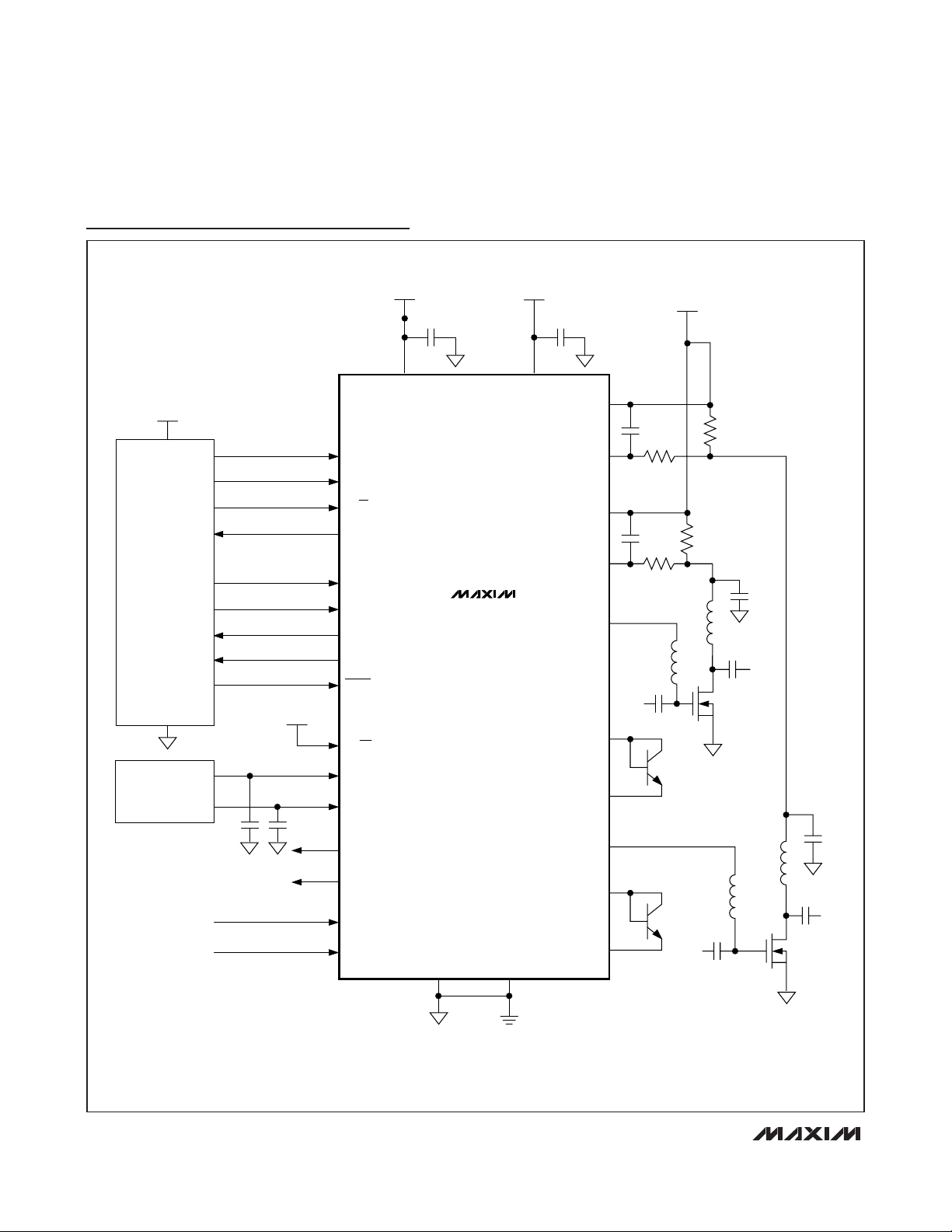
Typical Application Circuits—SPI Interface
5V
µC
DV
DD
0.1µF
DV
DD
SCL/SCLK
SDA/DIN
A0/CS
A1/DOUT
OPSAFE1
OPSAFE2
ALARM
BUSY
CNVST
DV
DD
SPI/I2C
MAX11008
AV
DD
0.1µF
AV
DD
CS1+
CS1-
CS2+
CS2-
GATE2
RF IN
DXP2
32V
C
*
F
RF*
C
*
F
RF*
R
SENSE
R
SENSE
LDMOS 1
RF OUT
EXTERNAL
2.5V
REFERENCE
0.1µF
0.1µF
*SELECT RF AND CF BASED ON DESIRED FILTER CUTOFF FREQUENCY WHERE f
LIMIT R
REFADC
REFDAC
PGAOUT1
PGAOUT2
ADCIN1
ADCIN2
DGND AGND
TO 100Ω TO MINIMIZE OFFSET ERRORS.
F
GATE1
CUTOFF
DXN2
DXP1
DXN1
= 1/(2 π RFCF).
RF IN
RF OUT
LDMOS 2
Page 17
Detailed Description
The MAX11008 sets and controls the bias conditions
for dual RF LDMOS power devices found in cellular
base-station power amps. Each device includes two
high-side current-sense amplifiers with programmable
gains of 2, 10, and 25 to monitor the LDMOS transistor
drain current over the 20mA to 5A range. Two external
diode-connected transistors monitor the LDMOS transistor temperatures while an internal temperature sensor measures the local die temperature of the
MAX11008. The 12-bit ADC is interfaced to a 7:1 multiplexer and converts the signals from the PGA outputs,
internal and external temperature readings, or the two
auxiliary analog inputs into digital data results that can
be stored in the FIFO.
On the control side, two gate-drive channels, driven
from two 12-bit DACs and a gain stage of 2, generate a
positive gate voltage bias for the LDMOS. Each gatedrive output supports up to ±2mA of gate current. The
gate-drive amplifier is current-limited to ±25mA and
features a fast clamp to analog ground that operates
independently of the serial interface.
The MAX11008 includes an on-chip, nonvolatile
EEPROM that stores LUTs and register information. The
LUTs are designed to store gate voltage vs. temperature
curves for the LDMOS FET. The data is used for temperature compensation of the LDMOS FET’s bias point.
The LUTs can also contain compensation data for another independent parameter: either sense voltage or
AIN voltage.
Digital Serial Interface
The MAX11008 features both an I2C and an SPI-compatible serial interface. Connect SPI/I2C to DGND to
select the I2C serial-interface operation, or to DVDDto
select the SPI serial-interface operation. Do not alter
interface mode during operation.
SPI Serial Interface
Connect SPI/I2C to DVDDto select the SPI interface.
The SPI serial interface consists of a serial data input
(DIN), a serial clock line (SCLK), a chip select (CS),
and a serial data output (DOUT). The use of serial data
output (DOUT) is optional and is only required when
data is to be read back by the master device. The
MAX11008 is SPI compatible within the range of VDD=
+2.7V to +5.25V. DIN, SCLK, CS, and DOUT facilitate
bidirectional communication between the MAX11008
and the master at rates up to 20MHz.
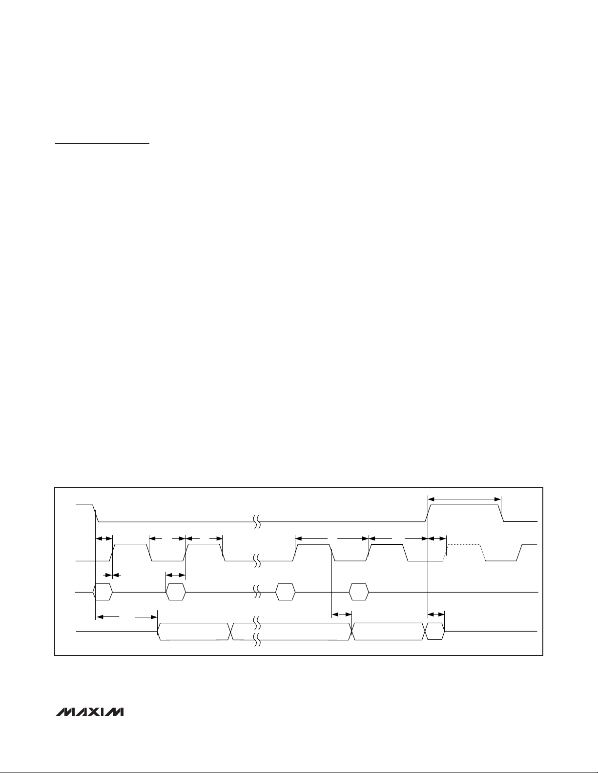
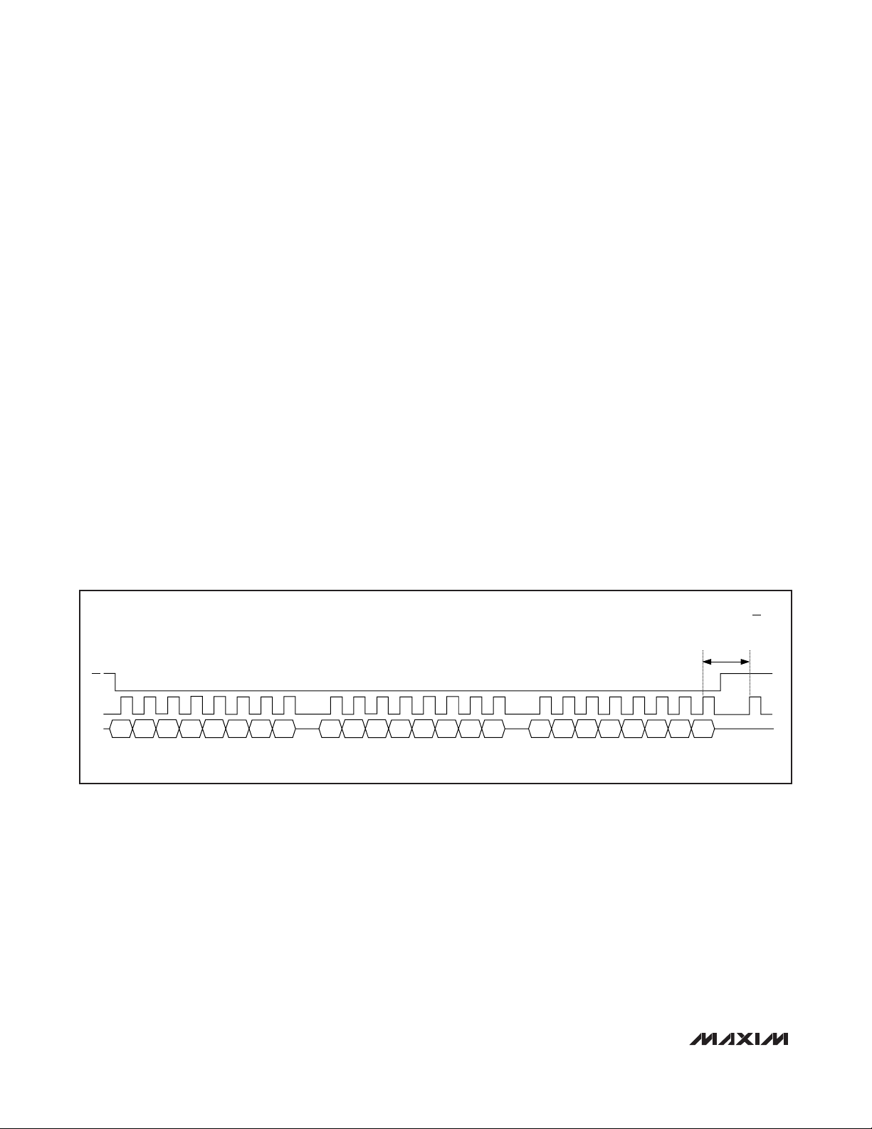
Figure 1 illustrates the 4-wire interface timing diagram.
The MAX11008 is a transmit/receive slave-only device,
relying upon a master to generate a clock signal. The
master initiates data transfer on the bus and generates
the SCLK signal to permit data transfer.
MAX11008
Dual RF LDMOS Bias Controller with
Nonvolatile Memory
______________________________________________________________________________________ 17
Figure 1. SPI Serial-Interface Timing
CS
t
CSS
SCLK
t
DH
DIN
DOUT
D23
t
DV
t
CL
t
DS
D22 D1 D0
t
CSW
t
t
CH
t
CP
t
DO
t
CSH
CSS
t
TR
Page 18
MAX11008
The SPI bus cycles are 24 bits long. Data can be supplied as three 8-bit bytes or as a continuous 24-bit
stream. CS must remain low throughout the 24-bit
sequence. The first 8-bit byte is a command byte
C[7:0]. The next 16 bits are data bits D[15:0]. Clock
signal SCLK can idle low or high, but data is always
clocked in on the rising edge of SCLK (CPOL = CPHA).
SPI data transfers begin with the falling edge of CS.
Data is clocked into the device on the rising edges of
SCLK and clocked out of the device on the falling
edges of SCLK. For correct bus cycles, CS should
frame the data and should not return to a 1 until after
the last active rising clock edge. See Figure 2 for timing
details. A rising edge of CS causes DOUT to threestate and data reads should be performed accordingly.
See Figures 1 and 3.
When writing instructions to the MAX11008, 24 clock
cycles must be completed before CS is driven high.
The MAX11008 executes the instruction only after the
24th clock cycle has been received and CS is driven
high. To abort unwanted instructions, CS can be driven
high at any time before the 23rd rising clock edge.
When reading data from the MAX11008, 24 clock
cycles must be completed before CS is driven high. If
CS is driven high before the completion of the 24th
falling edge, DOUT immediately three-states, the interface resets in preparation for the next command, and
the data being read is lost.
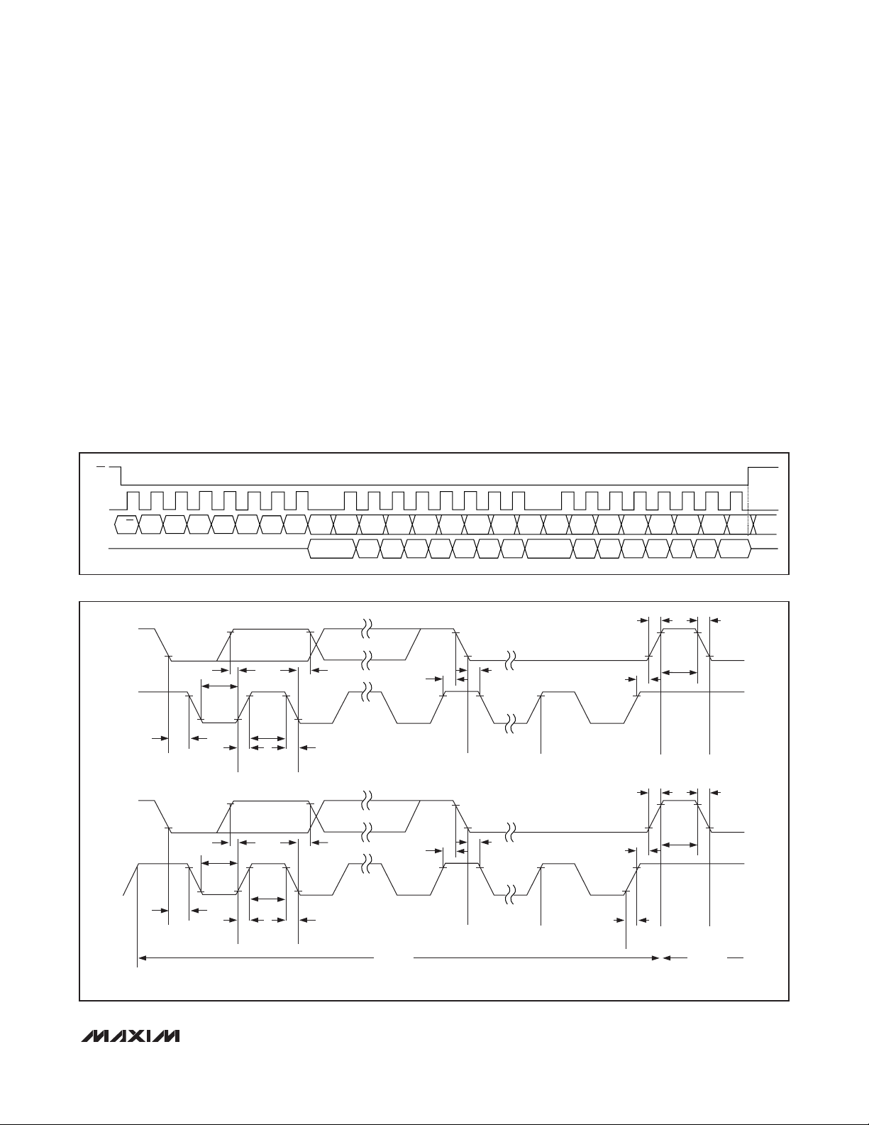
Write Format
Use the following sequence to write 16 bits of data to a
MAX11008 register (see Figure 2):
1) Drive CS low to select the device.
2) Send the appropriate write command byte (see
Table 6 for the register address map). The command byte is clocked in on the rising edge of SCLK.
3) Send 16 bits of data D[15:0] starting with the most
significant bit (MSB). Data is clocked in on the rising
edges of SCLK.
4) Drive CS high to conclude the command.
Dual RF LDMOS Bias Controller with
Nonvolatile Memory
18 ______________________________________________________________________________________
Figure 2. SPI Write Sequence
A RISING EDGE OF CS
DURING THIS PERIOD
COMPLETES A VALID WRITE
COMMAND
CS
SCLK
DIN
C6CR/W- C4C5 C2C3 C0C1
D15D14D13D12D11D10D9D8 D7D6D5D4D3D2D1D0
Page 19
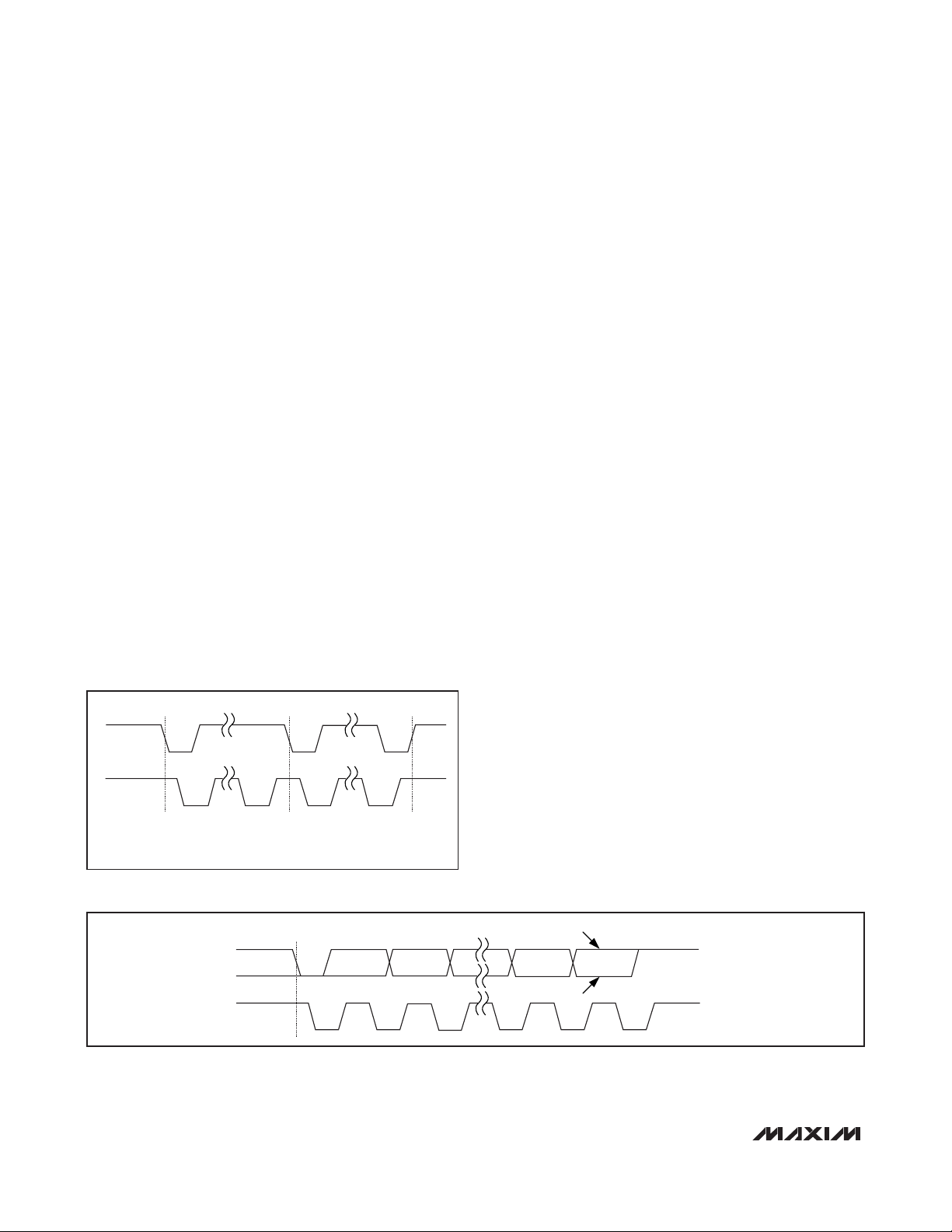
Read Format
Use the following sequence to read 16 bits of data from
a MAX11008 register (see Figure 3):
1) Drive CS low to select the device.
2) Send the appropriate read command byte (see
Table 6 for the register address map). The command byte is clocked in on the rising edges of
SCLK.
3) Receive 16 bits of data. The first 4 bits of data are
always high. Data is clocked out on the falling edges
of SCLK.
4) Drive CS high.
I2C Serial Interface
Connect SPI/I2C to DGND to select the I2C interface. The
I2C serial interface consists of a serial data line (SDA)
and a serial clock line (SCL). The MAX11008 is I2C compatible within the DV
DD
= 2.7V to 5.25V range. SDA and
SCL facilitate bidirectional communication between the
MAX11008 and the master at rates up to 400kHz for fast
mode and up to 3.4MHz for high-speed mode (HS
mode). See the
Bus Timing
and
HS I2C Mode
sections
for more information on data-rate configurations.
Figure 4 shows the 2-wire interface timing diagram. The
MAX11008 is a transmit/receive slave-only device, relying upon a master to generate a clock signal. The master (typically a microcontroller) initiates data transfers
on the bus and generates the SCL signal to permit data
transfer.
MAX11008
Dual RF LDMOS Bias Controller with
Nonvolatile Memory
______________________________________________________________________________________ 19
Figure 3. SPI Read Sequence
Figure 4. I2C Serial-Interface Timing Diagram
CS
SCLK
DIN
DOUT
C6R/W C4C5 C2C3 C0C1
a) F/S-MODE I
SDA
2
C SERIAL INTERFACE TIMING
t
SU, DAT
t
LOW
XXXXXXXXXXXX XXXXX
D14 D13 D12 D11 D10 D9 D8 D6 D5 D4 D3 D2 D1D15 D7 D0
t
HD, DAT
t
SU, STA
X
t
HD, STA
t
SU, ST0
t
R
t
F
t
BUF
SCL
t
t
HD, STA
S
2
b) HS-MODE I
SDA
PARAMETERS ARE MEASURED FROM 30% TO 70%.
C SERIAL INTERFACE TIMING
t
SU, DAT
t
LOW
SCL
t
HD, STA
t
S Sr A
RCL
HIGH
t
R
t
HIGH
t
F
Sr A
t
HD, DAT
t
RCL
t
SU, STA
t
HD, STA
t
SU, ST0
t
RCL
PS
t
RDA
P
t
RDA
t
BUF
S
F/S MODEHS MODE
Page 20
MAX11008
A master device communicates to the MAX11008 by
transmitting the proper slave address followed by a
command and/or data words. Each transmit sequence
is framed by a START (S) or repeated START (Sr) condition and a STOP (P) condition. Each word transmitted
over the bus is 8 bits long and is always followed by an
acknowledge clock pulse.
The MAX11008 SDA and SCL drivers are open-drain
outputs, requiring a pullup resistor (750Ω or greater) to
generate a logic-high voltage (see the
Typical
Application Circuits
). Series resistors are optional for
noise filtering. These series resistors protect the input
stages of the MAX11008 from high-voltage spikes on
the bus line, and minimize crosstalk and undershoot of
the bus signals.
Bit Transfer
One data bit is transferred during each SCL clock
cycle. The data on SDA must remain stable during the
high period of the SCL clock pulse. Changes in SDA
while SCL is high are control signals (see the
START
and STOP Conditions
section). Both SDA and SCL idle
high when the I2C bus is not busy.
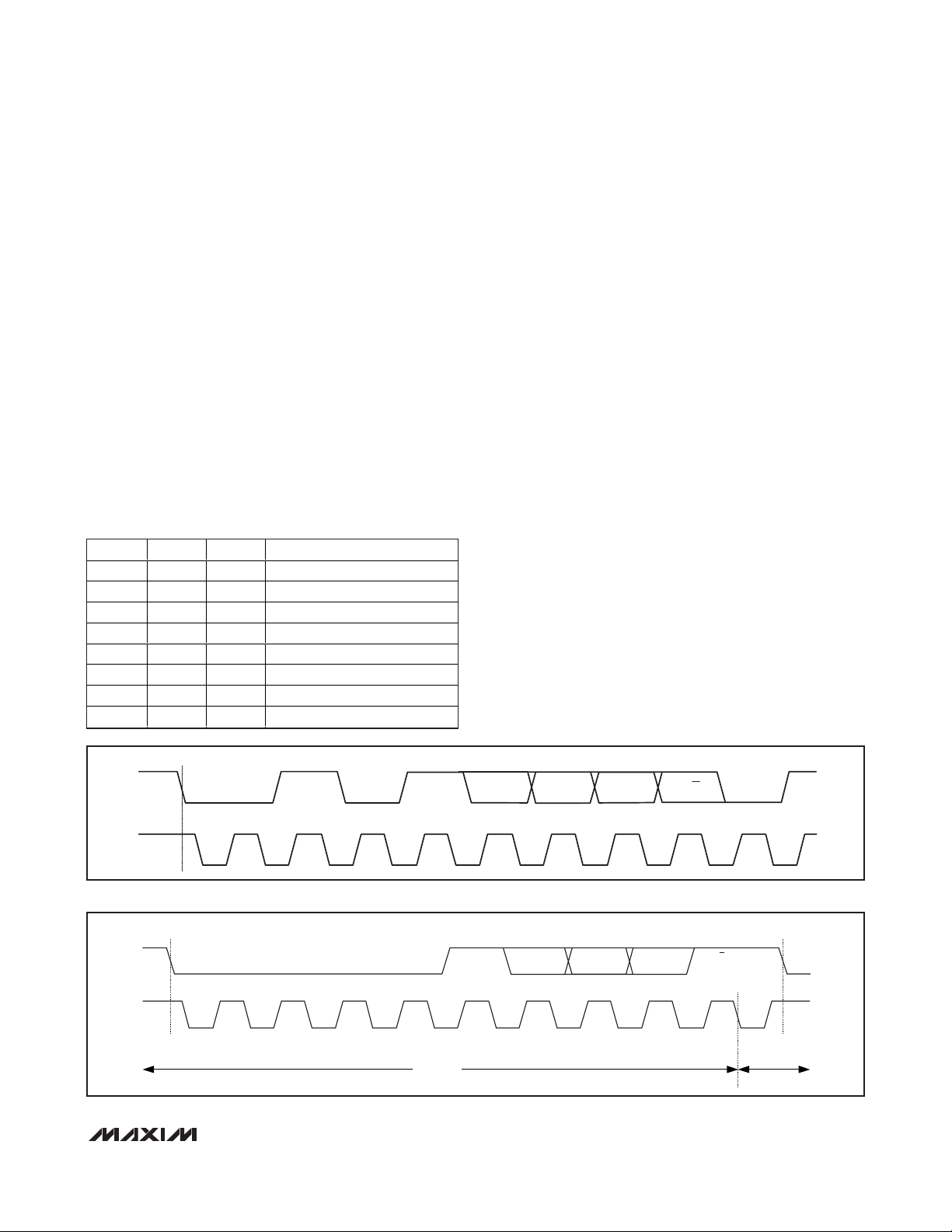
START and STOP Conditions
The master initiates a transmission with a START condition (S), which is a high-to-low transition on SDA while
SCL is high. The master terminates a transmission with
a STOP condition (P), which is a low-to-high transition
on SDA while SCL is high (see Figure 5). A repeated
START condition (Sr) can be used in place of a STOP
condition to leave the bus active and the mode
unchanged (see the
HS I2C Mode
section).
Acknowledge Bits and Not-Acknowledge Conditions
Data transfers are framed with an acknowledge bit
(ACK) or a not-acknowledge bit (NACK). Both the master and the MAX11008 (slave) generate acknowledge
bits. To generate an acknowledge, the receiving device
must pull SDA low before the rising edge of the
acknowledge-related clock pulse (ninth clock pulse)
and keep it low during the high period of the clock
pulse (see Figure 6).
To generate a not-acknowledge condition, the receiver
allows SDA to be pulled high before the rising edge of
the acknowledge-related clock pulse, and leaves SDA
high during the high period of the clock pulse.
Monitoring the acknowledge bits allows for detection of
unsuccessful data transfers. An unsuccessful data
transfer happens if a receiving device is busy or if a
system fault has occurred. In the event of an unsuccessful data transfer, the bus master reattempts communication at a later time.
Dual RF LDMOS Bias Controller with
Nonvolatile Memory
20 ______________________________________________________________________________________
Figure 5. START and STOP Conditions
Figure 6. Acknowledge Bits
SSrP
SDA
SCL
S = START.
Sr = REPEATED START.
P = STOP.
S
SDA
SCL
12 8
NOT ACKNOWLEDGE
ACKNOWLEDGE
9
Page 21
Slave Address
A bus master initiates communication with a slave
device by issuing a START condition followed by the 7bit slave address and a read/write (R/W) bit (see Figure
7). When the device recognizes its slave address, it is
ready to accept or send data depending on the R/W
bit. When the MAX11008 recognizes its slave address,
it issues an ACK by pulling SDA low for one clock cycle
and is ready to accept or send data depending on the
R/W bit that was sent.
The MAX11008 has eight user-selectable slave addresses, which are set through inputs A0, A1, and A2 (see
Table 1). This feature allows up to eight MAX11008
devices to share the same bus inputs. The 4 MSBs D[7:4]
are factory set, and the 3 LSBs are user-selectable.
Bus Timing
At power-up, the bus timing is set for I2C fast-mode
(F/S mode), which allows I2C clock rates up to 400kHz.
The MAX11008 can also operate in high-speed mode
(HS mode) to achieve I
2
C clock rates up to 3.4MHz.
See Figure 4 for I2C bus timing.
HS I2C Mode
Select HS mode by addressing all devices on the bus
with the HS-mode master code 0000 1XXX (X = don’t
care). After successfully receiving the HS-mode master
code, the MAX11008 issues a NACK, allowing SDA to
be pulled high for one clock cycle (see Figure 8). After
the NACK, the MAX11008 operates in HS mode. The
master must then send a repeated START (Sr) followed
by a slave address to initiate HS-mode communication.
If the master generates a STOP condition, the
MAX11008
Dual RF LDMOS Bias Controller with
Nonvolatile Memory
______________________________________________________________________________________ 21
Figure 7. Slave Address Bits
Figure 8. F/S-Mode to HS-Mode Transfer
Table 1. Slave Address Select
A2 A1 A0 ADDRESS
0 0 0 0101000
0 0 1 0101001
0 1 0 0101010
0 1 1 0101011
1 0 0 0101100
1 0 1 0101101
1 1 0 0101110
1 1 1 0101111
S
SDA
SCL
SDA
0 0 A2 A1 A0
12
0000
1234
1
1
34 5 67 89
1XXX9A
5678
F/S MODE
R/W A
Sr
HS MODE
Page 22

MAX11008
MAX11008 returns to F/S mode. Use a repeated START
condition in place of a STOP condition to leave the bus
active and the mode unchanged. Figure 9 summarizes
the data bit transfer format for HS-mode communication.
Register Address/Data Bytes (Write Cycle)
A write cycle begins with the bus master issuing a
START condition followed by 7 address bits (see Figure
5 and Table 1) and a write bit (R/W = 0). Once the
slave address is recognized and the write bit is
received, the MAX11008 (I2C slave) issues an ACK by
pulling SDA low for one clock cycle. The master then
sends the register address byte (command byte) to the
slave. The MSB of the register address byte is the
read/write bit for the destination register address of the
slave and must be set to 0 for a write cycle (see the
Register Address Map
section). After receiving the
byte, the slave issues another acknowledge, pulling
SDA low for one clock cycle. The master then writes
two data bytes, receiving an ACK from the slave after
each byte is sent. The master ends the write cycle by
issuing a STOP condition. When operating in HS mode,
a STOP condition returns the bus into F/S mode (see
the
HS I2C Mode
section). Figure 10 shows a complete
write cycle.
Dual RF LDMOS Bias Controller with
Nonvolatile Memory
22 ______________________________________________________________________________________
Figure 9. Data-Transfer Format in HS Mode
Figure 10. Write Cycle
MASTER TO SLAVE
SLAVE TO MASTER
F/S MODE HS MODE
S
MASTER CODE
N Sr SLAVE ADDRESS R/W A DATA A P
F/S MODE
N BYTES + ACK
HS MODE CONTINUES
MASTER TO SLAVE
SLAVE TO MASTER
4-BYTE WRITE CYCLE
1
S
711
SLAVE
ADDRESS
A
W
8
REGISTER ADDRESS
BYTE
WHETHER TO READ OR WRITE TO
A1DATA BYTE
MSB DETERMINES
REGISTERS
Sr SLAVE ADD
8
A1DATA BYTE
8
1
A
P OR Sr
1
NUMBER OF BITS
Page 23

Register Address/Data Bytes (5-Byte Read Cycle)
A read cycle begins with the master issuing a START
condition followed by a 7-bit address, (see Figure 5
and Table 1) and a write bit (R/W = 0) to instruct the
MAX11008 interface that it is about to receive data.
Once the slave address is recognized and the write bit
is received, the MAX11008 (I2C slave) issues an ACK
by pulling SDA low for one clock cycle. The master
then sends the register address byte (command byte)
to the slave. The MSB of the register address byte is
the read/write bit for the destination register address of
the slave and must be set to 1 for a read cycle (see the
Register Address Map
section). After this byte is
received, another acknowledge bit is sent to the master
from the slave. The master then issues a repeated
START (Sr) condition. Following a repeated START (Sr),
the master writes the slave address byte again with a
read bit (R/W = 1). After a third acknowledge signal
from the slave, the data direction on the SDA bus
reverses and the slave writes the 2 data bytes (the
contents of the register that was addressed in the previous command byte) to the master. Finally, the master
issues a NACK followed by a STOP condition (P), ending the read cycle. Figure 11 shows a complete 5-byte
read cycle.
Default Read Cycle (3-Byte Read Cycle)
The MAX11008 2-wire interface has a unique feature for
read commands. To avoid the necessity of sending 2
slave address bytes in one read cycle (see the 5-byte
read cycle in Figure 11), the MAX11008 2-wire interface
recognizes a single slave address byte with a read bit
(R/W = 1). In this case, the interface outputs the contents of the last read device register. This default read
feature is useful when the master must perform multiple
consecutive reads from the same device register.
Figure 11 shows a complete 3-byte read cycle.
MAX11008
Dual RF LDMOS Bias Controller with
Nonvolatile Memory
______________________________________________________________________________________ 23
Figure 11. 5-Byte and 3-Byte Read Cycle
MASTER TO SLAVE
SLAVE TO MASTER
5-BYTE READ CYCLE
1
S
3-BYTE READ CYCLE
1
711
SLAVE
ADDRESS
71
SLAVE
ADDRESS
RS
8
A
W COMMAND BYTE
1
A
8
DATA BYTE DATA BYTE
1
ASr
18
A
711
SLAVE
ADDRESS
81
DATA BYTE
AA
R
1
1
N
P OR Sr
NUMBER OF BITS
81
DATA BYTE
N
1
P OR Sr
NUMBER OF BITS
Page 24

MAX11008
12-Bit ADC
The MAX11008 12-bit ADC uses a SAR conversion
technique and on-chip track-and-hold (T/H) circuitry to
convert the PGA outputs (PGAOUT1 and PGAOUT2),
temperature measurements, and single-ended auxiliary
input voltages (ADCIN1 and ADCIN2) into 12-bit digital
data when in ADC monitor mode (see the
Hardware
Configuration Register (HCFIG) (Read/Write)
section).
All nontemperature measurements are converted using
a unipolar transfer function (see Figure 13), and all temperature measurements are converted using a bipolar
transfer function (see Figure 14).
Analog Input T/H
Figure 12 shows the equivalent circuit for the ADC input
architecture of the MAX11008. In track mode, an input
capacitor is connected to the input signal (ADCIN1,
ADCIN2, PGAOUT1, PGAOUT2, or temperature sensor
processor output). Another input capacitor is connected to AGND. After the T/H enters hold mode, the difference between the sampled positive and negative input
voltages is converted. The charging rate of the input
capacitance determines the time required for the T/H to
acquire an input signal. If the input signal’s source
impedance is high, the required acquisition time
lengthens accordingly.
Any source impedance below 300Ω does not affect the
ADC’s AC performance. A high-impedance source can
be accommodated either by lengthening t
ACQ
or by
placing a 1µF capacitor between the positive and negative analog inputs. The combination of the analoginput source impedance and the capacitance at the
analog input creates an RC filter that limits the analog
input bandwidth.
Input Bandwidth
The ADC’s input-tracking circuitry has a 1MHz smallsignal bandwidth, to digitize high-speed transient
events and measure periodic signals with bandwidths
exceeding the ADC’s sampling rate by using undersampling techniques. Anti-alias filtering of the input signals is necessary to prevent high-frequency
components from aliasing into the frequency band of
interest.
Analog Input Protection
Internal electrostatic-discharge (ESD) protection diodes
clamp all analog inputs to AVDDand AGND, allowing
the inputs to swing from (AGND - 0.3V) to (AVDD+
0.3V) without damage. However, for accurate conversions near full scale, the inputs must not exceed AV
DD
by more than 50mV or be lower than AGND by 50mV. If
an analog input voltage exceeds the supplies, limit the
input current to 2mA.
Dual RF LDMOS Bias Controller with
Nonvolatile Memory
24 ______________________________________________________________________________________
Figure 12. Analog Input Track and Hold
REFADC
ADCIN1
ADCIN2
PGAOUT1
PGAOUT2
TEMP SENSOR READING
AGND
ALL SWITCHES SHOWN IN TRACK MODE.
HOLD
TRACK
TRACK
CIN+
CIN-
HOLD
/2
AV
DD
CAPACITIVE
DAC
TRACK
COMPARATOR
HOLD
Page 25

ADC Transfer Functions
Figure 13 shows the unipolar transfer function for nontemperature measurements, and Figure 14 shows the
bipolar transfer function used for temperature measurements. Code transitions occur halfway between successive-integer LSB values. Output coding is binary,
with 1 LSB = V
REFADC
/4096 for nontemperature measurements, and 1 LSB = +0.125°C for temperature
measurements. All signed binary results use two’s complement format.
ADC Conversion Scheduling
The MAX11008 ADC multiplexer scans and converts
the selected inputs in the order shown in Table 2 (see
the
ADC Conversion Register (ADCCON) (Write Only)
section) when more than one channel is selected. The
results are stored in the FIFO when in ADC monitoring
mode. The BUSY signal is set at the start and reset at
the end of a scan except when the continuous convert
bit is set at which time BUSY does not then respond to
ADC conversions.
Writing a conversion command before a conversion is
complete cancels the pending conversion. Avoid
addressing the device using the serial interface while
the ADC is converting.
ADC Clock Modes
The MAX11008 offers three conversion/acquisition
modes (known as clock modes) selectable through
configuration register bits CKSEL1 and CKSEL0.
If the ADC conversion requires the internal reference
(temperature measurement or voltage measurement with
internal reference selected) and the reference has not
been previously forced on (FBGON = 1), the device
inserts a typical delay of 72µs, for the reference to settle,
before commencing the ADC conversion. The reference
remains powered up while there are pending conversions. If the reference is not forced on, it automatically
powers down at the end of a scan or when CONCONV in
the ADC Conversion register is set back to 0.
Internally Timed Acquisitions
and Conversions
Clock Mode 00
In clock mode 00, power-up, acquisition, conversion,
and power-down are all initiated by writing to the ADC
Conversion register and performed automatically using
the internal oscillator. This is the default clock mode.
The ADC sets the BUSY output high, powers up, and
scans all requested channels storing the results in the
FIFO if the ADCMON bit has been set. After the scan is
MAX11008
Dual RF LDMOS Bias Controller with
Nonvolatile Memory
______________________________________________________________________________________ 25
Figure 13. ADC Transfer Function
Figure 14. Temperature Transfer Function
Table 2. Order of ADC Conversion Scan
V
REFADC
1111 1111 1111
1111 1111 1110
1111 1111 1101
1111 1111 1100
BINARY OUTPUT CODE
0000 0000 0011
0000 0000 0010
0000 0000 0001
0000 0000 0000
0
0111 1111 1111
0111 1111 1110
0111 1111 1101
0000 0000 0001
OUTPUT CODE
0000 0000 0000
1111 1111 1111
1000 0000 0010
1000 0000 0001
1000 0000 0000
-256 +2550
FULL-SCALE TRANSITION
1 LSB = V
1 2 3 4093 4095
1 LSB = +0.125°C
/4096
REFADC
INPUT VOLTAGE (LSB)
TEMPERATURE (°C)
V
REFADC
ORDER OF SCAN DESCRIPTION OF CONVERSION
1 Internal device temperature
2 External diode 1 temperature
3 Output of PGA 1 for current sense
4 Auxiliary input 1 (ADCIN1)
5 External diode 2 temperature
6 Output of PGA 2 for current sense
7 Auxiliary input 2 (ADCIN2)
Page 26

MAX11008
complete the ADC powers down, BUSY is pulled low,
and the results for all of the selected channels are
available in the FIFO.
The duration of the BUSY pulse is additive, depending
on the channel conversion sequence selected. The
BUSY pulse is set typically for 72µs by temperature
conversions; 52µs by PGAOUT conversions, and 7µs
by ADCIN conversions.
Clock Mode 01
In clock mode 01, power-up, acquisition, conversion,
and power-down are all initiated through a single pulse
on CNVST and performed automatically using the inter-
nal oscillator. Initiate a scan by writing to the ADC conversion register and setting CNVST low for at least
20ns. The ADC sets the BUSY output high, powers up,
and scans all requested channels storing the results in
the FIFO if the ADCMON bit has been set. After the
scan is complete, the ADC powers down, BUSY is
pulled low, and the results for all of the selected channels are available in the FIFO. The BUSY pulse behavior is identical to that of clock mode 00.
Externally Timed
Acquisitions and Conversions
Clock Mode 10
Clock mode 10 is reserved. Do not use this clock
mode.
Clock Mode 11
In clock mode 11, set the FBGON bit. Conversions are
initiated one at a time through CNVST and performed
using the internal oscillator. In this mode, the acquisition
time is controlled by the time CNVST is low. CNVST is
resynchronized by the internal oscillator, resulting in a
one-clock cycle (typically 320ns) uncertainty in the exact
sampling instant. Different timing parameters apply
depending if the conversion is temperature, from ADCIN,
or from PGAOUT (as specified in the
Clock Mode 00
section). Figure 15 shows a conversion time example.
Both internal and external temperature conversions are
internally timed. Pull CNVST low for a minimum of 20ns
(t
CNV11
) to trigger a temperature conversion. The BUSY
output goes high and the temperature conversion result
is available in the FIFO (if the ADCMON bit is set) 72µs
(typ) after BUSY goes low again.
Dual RF LDMOS Bias Controller with
Nonvolatile Memory
26 ______________________________________________________________________________________
Figure 15. ADC Clock Mode 11 Example
INTERNAL TEMPERATURE READING, PGA1 OUTPUT, AND ADCIN1 CONVERSION TIMING IN CLOCK MODE 11
t
= 20ns (typ)
CNV
CNVST
= 1.5µs (typ)
t
= 30µs (typ)
t
ACQ
ACQ
BUSY
INTERNAL
OPERATIONS
WRITE TO ADC
CONVERT REGISTER TO
SET UP ADC SCAN
FBGON = 1,
ADCMON = 1
TEMPERATURE
CONVERSION
70µs (typ)
CONVERSION RESULT
AVAILABLE IN FIFO
IDLE MODE,
POWERED
TEMPERATURE
REF AND
TEMP
SENSOR
PGA 1
ACQUISITION
PGA 1
CONVERSION
22µs (typ)
RESULT AVAILABLE
IDLE MODE,
REF AND
SENSOR
POWERED
PGA 1 OUTPUT
CONVERSION
IN FIFO
TEMP
ADCIN1
ADCIN1
CONVERSION
ACQUISITION
ADCIN 1
CONVERSION
RESULT AVAILABLE
IN FIFO
7µs (typ)
END OF
SCAN
Page 27

For a PGAOUT conversion, set CNVST low for a minimum of 30µs or maximum of 40µs. The BUSY output
goes high at the start of the CNVST pulse and the
PGAOUT conversion result is available in the FIFO (if the
ADCMON bit has been set) 52µs (typ) after BUSY goes
low again.
For an ADCIN conversion, set CNVST low for at least
1.5µs. The BUSY output goes high at the end of the
CNVST pulse and the ADCIN conversion result is available in the FIFO (if the ADCMON bit is set) 7µs (typ) after
BUSY goes low again.
For ease of operation, all CNVST pulses can use a 30µs
width irrespective of the source being converted. In the
case of ADC conversions, the BUSY pulse width is
extended accordingly. For clock modes 00 and 01, the
BUSY pulse width duration depends on the channel conversion sequence selected.
Continuous conversion is not supported in this clock
mode (see Table 20 for the ADC Conversion register).
Changing Clock Modes During ADC Conversions
If a change is made to the clock mode in the configuration register while the ADC is already performing a conversion (or series of conversions), the following
describes how the MAX11008 responds:
• When CKSEL = 00 and is then changed to another
value, the ADC completes the already triggered series
of conversions and then goes idle. The BUSY output
remains high until the conversions are completed. The
MAX11008 then responds in accordance with the new
CKSEL mode.
• When CKSEL = 01 and is then changed to another
value and if the device is waiting for the initial external
trigger, the MAX11008 immediately exits clock mode
01, powers down the ADC, and goes idle. The BUSY
output stays low and the new clock mode is observed.
If a conversion sequence has started, the ADC completes the requested conversions and then goes idle.
The BUSY output remains high until the conversions
are completed. The MAX11008 then responds in
accordance with the new CKSEL mode.
• When CKSEL = 11 and is then changed to another
value and if the device is waiting for an external trigger, the MAX11008 immediately exits clock mode 11,
powers down the ADC, and goes idle. The BUSY output stays low and the new clock mode is observed.
Turning the Continuous Conversion Bit
(CONCONV) On and Off
When switching between continuous and single conversion modes, the clock mode requires resetting to avoid
hanging the ADC sequencing routine.
For example, the following is the command sequence to
switch from continuous to single conversion and revert to
continuous conversion:
1) Write ADCCON (00000000 10110111).
2) Turn off the selected channels, but leave the continuous convert bit asserted. Write ADCCON (00000000
10000000).
3) Turn off the continuous convert bit. Write ADCCON
(00000000 00000000).
4) Change from the current clock mode (00 in this case)
to any other one. Write HCFIG (00000100 00011000).
5) Change the clock mode back. Write HCFIG
(00000100 00001000).
6) Clear the FIFO. Write SCLR (00000000 00000100).
7) Perform the single conversion. Write ADCCON
(00000000 00110111).
8) Read the FIFO five times to capture the results of the
single conversions. Read FIFO.
9) Turn continuous convert back on. Write ADCCON
(00000000 10110111).
The alternative to this command sequence is to leave
continuous conversion on and just read the FIFO. When
using this method, decode the channel tag to determine
which channel has been read.
12-Bit DACs
In addition to the 12-bit ADC, the MAX11008 also
includes two voltage-output, 12-bit, monotonic DACs
with typically less than ±2 LSB integral nonlinearity
error and less than ±1 LSB differential nonlinearity
error. Each DAC also has a 45ms settling time and
ultra-low glitch energy (4nV·s). The 12-bit DAC codes
are unipolar binary with 1 LSB = V
REFDAC
/4096.
MAX11008
Dual RF LDMOS Bias Controller with
Nonvolatile Memory
______________________________________________________________________________________ 27
Page 28

MAX11008
Figure 16 shows the functional diagram of the
MAX11008 DACs. Each DAC includes an input and
output register. The input registers hold the result of the
most recent write operation, and the output registers
hold the current output code for the respective DAC.
Data written to a DAC input register is transferred to its
output register by writing to the Load DAC register (see
Table 22). Alternatively, write data directly to the output
register using the DAC Input and Output Data register.
The analog output voltages of the DACs (before amplification by the gate-drive amplifiers) are calculated with
the following equation:
where V
DACREF
is the value of the internal or external
reference voltage and CODE is the decimal value of the
12-bit code contained in the output register.
Gate-Drive Amplifiers
The gate-drive amplifiers are proportional to the analog
outputs of the 12-bit DACs and provide the necessary
gate voltage to drive the external LDMOS transistors.
Both amplifiers have a fixed gain of 2V/V and are capable of sourcing or sinking up to 2mA of current. Output
short-circuit protection prevents output currents from
exceeding ±25mA.
The gate output is equal to the DAC output voltage
amplified by 2.
V
GATE_
= 2 x V
DAC
See the
Software Configuration Registers
and
Temperature/APC LUT Configuration Registers
sections
for information on how the gate voltages are controlled
by temperature and APC samples.
Output Clamp
The MAX11008 features an output clamp mode that
protects the external LDMOS transistors by connecting
the gate-drive amplifier outputs (GATE_) to AGND. The
clamp mode can be controlled by the OPSAFE_ digital
inputs or by setting the appropriate ALMCLMP[1:0] bits
in the Alarm Hardware Configuration register (see
Table 14). When using the OPSAFE_ digital inputs, pull
OPSAFE_ high to enter clamp mode and pull OPSAFE_
low to exit clamp mode. The clamp can also be activated automatically from the alarm trip point setting registers; see the
Alarm Software Configuration Register
(ALMSCFIG) (Read/Write)
section.
Self-Calibration
Calibrate channel 1 and channel 2 by writing to the
PGA Calibration Control register. The MAX11008 functions after power-up without a calibration. Command a
calibration after powering up the device by setting the
TRACK bit to 0 and the DOCAL bit to 1 (see Table 19).
Subsequently, set the TRACK, DOCAL, and SELFTIME
bits to 1 to enable automatic self-calibration (approximately every 13ms). This minimizes loss of performance over temperature and supply-voltage variation.
Alternatively, run self-calibration manually to control the
timing of the operation. Set the TRACK and DOCAL bits
to 1 and the SELFTIME bit to 0 to perform manually triggered self-calibration.
The self-calibration algorithm cancels offsets at the
PGA-drive amplifier inputs in approximately 50µV increments to improve accuracy. The self-calibration routine
can be commanded when the DACs are powered
down, but the results will not be accurate. For best
results, run the calibration after the DAC power-up time,
t
DPUEXT
. The ADC’s operation is suspended during a
self-calibration. The BUSY output returning low indicates the end of the self-calibration routine. Wait until
the end of the self-calibration routine before requesting
an ADC conversion.
Dual RF LDMOS Bias Controller with
Nonvolatile Memory
28 ______________________________________________________________________________________
Figure 16. DAC Functional Diagram
V CODE
=
DACREF
V
DAC
×
4096
CHANNEL 1/CHANNEL 2
DAC INPUT REGISTERS
LDDACCH_
SET TO 1 IN
LOAD DAC
REGISTER
CHANNEL 1/CHANNEL 2
Channel 1/Channel 2
DAC OUTPUT REGISTERS
CHANNEL 1/
CHANNEL 2 DAC
Page 29

ADC and DAC References
The MAX11008 provides an internal low-noise +2.5V
reference for the ADCs, DACs and temperature sensor.
When using the internal reference the REFDAC and
REFADC inputs can either be left open or to improve
noise performance, bypassed with a 0.1µF capacitor to
AGND. Connect a voltage source to the REFADC input
ranging between +1V to AVDDto configure the device
for external ADC reference mode. Connect a voltage
source to the REFDAC input ranging between +0.7V to
+2.5V to configure the device for external DAC reference mode. When using an external voltage reference,
bypass the REFDAC and REFADC inputs with a 0.1µF
capacitor to AGND. Bits D[3:0] within the Hardware
Configuration register control the source of the DAC
and ADC references. See Table 11.
Temperature Sensors
The MAX11008 measures the internal die temperature
and two external LDMOS transistor temperatures through
one internal and two external diode-connected transistors. The MAX11008 performs temperature measurements by changing the bias current of each diode from
4µA to 68µA to produce a temperature-dependent bias
voltage difference. The internal ADC converts the voltage difference to a digital value. The conversion result at
4µA is subtracted from the conversion results at 68µA to
calculate a digital value that is proportional to absolute
temperature. The output data sent to the master will be
the resultant digital code minus an offset value to adjust
from Kelvin to Celsius. Temperature data is delivered to
the master as a 12-bit signed (two’s complement) fractional number with the 3 LSBs being the fractional bits.
This provides a temperature measurement resolution of
1/8°C. See Table 3 for examples of the signed fractional
number digital temperature codes.
In clock mode 00, initiate temperature conversions by
writing 0x13 to the ADC Conversion register. In clock
mode 01, initiate temperature conversions by writing
0x13 to the ADC Conversion register and pulse CNVST
low. In clock mode 11, initiate temperature conversions
by writing 0x13 to the ADC Conversion register and
pulse CNVST low for each channel conversion. Set the
corresponding data bits for the temperature sensor to
be measured to 1 (see the
ADC Conversion Register
(ADCCON) (Write Only)
section and Table 20) for all
three clock modes. Set the high and low external temperature thresholds through the temperature threshold
registers. See the
Low Temperature Threshold
Registers (TL1, TL2) (Read/Write)
section,
High
Temperature Threshold Registers (TH1, TH2)
(Read/Write)
section, and Tables 7 and 8).
The reference voltage for the temperature measurements is always derived from the internal reference
source to ensure that 1 LSB corresponds to 1/8 of a
degree Celsius. On every scan where only temperature
measurements are requested, temperature conversions
are carried out in the following order: INTEMP,
EXTEMP1, then EXTEMP2. If the ADCMON bit is set
when the conversions are performed, the temperature
readings are available in the FIFO.
The temperature-sensing circuits power up at the start
of an ADC conversion scan. The temperature-sensing
circuits remain powered on until the end of the scan to
avoid a 50µs delay caused by the internal reference
power-up time required for each individual temperature
channel. The temperature-sensor circuits remain powered up when the ADC conversion register’s continuous convert bit (CONCONV, see Table 20) is set to 1
and the current ADC conversion includes a temperature channel. The temperature-sensor circuits remain
powered up until the CONCONV bit is set low.
The external temperature-sensor drive current ratio has
been optimized for a 2N3904 npn transistor with an ideality factor of 1.0065. The nonideality offset is removed
internally by a preset digital coefficient. Using a transistor with a different ideality factor produces a proportionate difference in the absolute measured temperature.
For more details on this topic and others related to
using an external temperature sensor, refer to
Application Note 1057:
Compensating for Ideality
Factor and Series Resistance Differences between
Thermal Sense Diodes
and Application Note 1944:
Temperature Monitoring Using the MAX1253/54 and
MAX1153/54
.
MAX11008
Dual RF LDMOS Bias Controller with
Nonvolatile Memory
______________________________________________________________________________________ 29
Table 3. Signed Fractional Number
Temperature-Code Examples
TEMPERATURE
(°C)
-40 1110 1100 0000
-1.625 1111 1111 0011
0 0000 0000 0000
+27.125 0000 1101 1001
+105 0011 0100 1000
DIGITAL CODE
[D11:0]
Page 30

MAX11008
High-Side Current-Sense
Amplifiers and PGAs
The MAX11008 provides dual high-side current-sense
and differential amplifier capability. The current-sense
amplifiers provide a 5V to 32V input common-mode
range. Both CS_+ and CS_- must be within the specified common-mode range for proper operation of each
amplifier.
The sense amplifiers measure the load current, I
LOAD
,
through an external sense resistor, R
SENSE
, between
the CS_+ and CS_- inputs. The full-scale sense voltage
range (V
SENSE
= V
CS_+
- V
CS_-
) depends on the pro-
grammed gain (see the
Electrical Characteristics
section). The sense amplifiers provide a voltage output at
PGAOUT1 and/or PGAOUT2, where the output voltage
is determined by the following equation:
V
PGAOUT_
= A
PGA
x (V
CS_+
- V
CS_-
)
where A
PGA
is the selected gain setting of the PGA (2,
10, or 25).
The PGA outputs are routed to the internal 12-bit ADC to
internally monitor and/or read through the serial interface.
The PGA scales the sensed voltages to fit the input range
for the ADC. Program the PGA with gains of 2, 10, and 25
by setting the PG_SET_ bits in the Hardware
Configuration register (see Tables 11 and 11c).
To increase the accuracy of drain current measurements, the MAX11008 features a PGA output offset voltage calibration function. The PGA calibration function
has two modes of operation: acquisition mode and
tracking mode. In acquisition mode, the calibration routine operates continuously until the offset error of the
PGA is minimized. In tracking mode, the calibration
routine operates intermittently and has higher noise
thresholds (more averaging). Typically, the first calibration is performed in acquisition mode and all subsequent calibrations are performed in tracking mode. The
PGA Calibration Control register selects the PGA calibration mode and controls when calibrations occur
(see the
PGA Calibration Control Register (PGACAL)
(Write Only)
section).
Since PGA calibration affects the accuracy of ADC
conversion results, avoid performing PGA calibrations
when ADC conversions are in progress. Wait at least
2µs (t
DPUEXT
) after DAC power-up before performing a
PGA calibration.
First-In-First-Out (FIFO)
The MAX11008 utilizes a bidirectional FIFO that can
store up to eight 16-bit data words. The data stored in
the FIFO may consist of ADC conversion results (see
the
ADC Monitoring Mode
section), user data that is to
be written to the EEPROM (see the
LUT Streaming
Mode
section), or data that is to be read from the
EEPROM (see the
Message Mode
section). The data
remains in the FIFO until it can be read by the master
device through the serial data line (see the
ADC
Monitoring Mode
or
Message Mode
section) or written
to the EEPROM (see the
LUT Streaming Mode
section).
The proceeding sections describe the various modes
of operation and data flow control that involve the FIFO.
ADC Monitoring Mode
Setting the ADCMON (D10) bit in the Hardware
Configuration register (see Table 11) places the
MAX11008 into ADC monitoring mode. The 12-bit ADC
conversion result of the selected channel is placed into
the FIFO along with a 4-bit channel tag. The 4-bit channel tag is primarily used to indicate the origin of the
conversion, and can also be used to indicate that the
conversion data may be corrupted during FIFO overflow or that the FIFO is currently empty (see Tables 24
and 24a).
When multiple conversions are made, the FIFO may
overflow if data is placed into the FIFO faster than it is
read out. In this case, the FIFO stores the seven most
recent ADC conversions. When the 8th conversion
result enters the FIFO, the oldest conversion is discarded, thereby leaving the seven most recent results. The
FIFOOVER bit (D8) in the Flag register (see Table 26) is
set to 1 when FIFO overflow occurs.
If the FIFO is full and overflowing on each ADC conversion, there is a narrow timing window in which reading
the FIFO produces invalid data. The MAX11008 detects
this hazard and flags the data as unreliable by using
the channel tag error (1110). Only the data being read
through the serial interface is invalid. The ADC sample
used internally for V
GATE_
calculations is valid. To avoid
overflow, systematically remove data from the FIFO.
If the ADC data is read out of the FIFO faster than data
is transferred into the FIFO, essentially emptying the
FIFO, a data word containing the empty FIFO tag
(1111) and the current status of the Flag register is
read from the FIFO.
LUT Streaming Mode
The LUT streaming mode is used to write data to the
EEPROM. Place the MAX11008 in LUT streaming mode
by writing to the LUT Streaming register (see Table 27)
and disabling the internal watchdog oscillator in the
Software Shutdown register. The FIFO is cleared when
entering LUT streaming mode, so important data
remaining in the FIFO should be read before entering
this mode. Write the data that is to be transferred to the
EEPROM to the FIFO. The MAX11008 automatically
Dual RF LDMOS Bias Controller with
Nonvolatile Memory
30 ______________________________________________________________________________________
Page 31

MAX11008
Dual RF LDMOS Bias Controller with
Nonvolatile Memory
______________________________________________________________________________________ 31
moves the data from the FIFO and writes it to the
EEPROM. The MAX11008 remains in LUT streaming
mode until the specified amount of data is written to the
EEPROM. Set the internal watchdog oscillator when
LUT streaming mode is exited. If the FIFO is emptied
before all of the data is written to the EEPROM, the
MAX11008 waits until more data is placed into the
FIFO. If data is placed into the FIFO faster than it can
be written to the EEPROM causing the FIFO to fill completely, the FIFOOVER bit in the Flag register is set to 1
and all subsequent writes to the FIFO are ignored until
there is space for another data word.
The BUSY output goes high during LUT streaming
mode and returns low after all of the data is written to
the EEPROM.
FIFO data flow control in the LUT streaming mode can
be implemented with the following methods:
1) Open Loop—Write data to the FIFO at a rate that
does not exceed 1 word per 60µs to guarantee that
the FIFO does not overflow.
2) Software Flow Control—Check the FIFOOVER bit
(D8) in the Flag register (see Table 26) in between
FIFO write commands to ensure that the FIFO is not
full; then write data to the FIFO.
3) FIFO Status Monitoring—By setting the FIFOSTAT bit
(D11) to 1 in the Hardware Configuration register,
the ALARM output is used to indicate FIFO status.
When the FIFO is full, the ALARM output goes low
and returns high when there is space in the FIFO for
another data word. See Figures 17 and 18.
Message Mode
Use the message mode to read data from the
EEPROM. Write to the user Message register to place
the MAX11008 into message mode (see Table 23). The
FIFO is cleared when entering message mode, so
important data contained in the FIFO should be read
before entering this mode. The specified EEPROM data
is copied into the FIFO and is read by issuing a FIFO
read command. The MAX11008 remains in message
mode until all of the specified EEPROM data is copied
into and read from the FIFO. If the EEPROM data is
copied into the FIFO faster than it is read causing the
FIFO to fill completely, the copying action is suspended
until a data word is read out of the FIFO and the
FIFOOVER bit is set to indicate a not-full condition. If
the EEPROM data is read out of the FIFO faster than it
can be copied causing the FIFO to empty completely, a
data word containing the empty FIFO tag (1111) and
current status of the Flag register is read from the FIFO.
This underflow data is indistinguishable from arbitrary
EEPROM data, so it is necessary to use data flow-control methods to safely read the EEPROM.
The BUSY output goes high during message mode and
returns low after all of the specified EEPROM data is
read from the FIFO.
FIFO data flow control in message mode can be implemented with the following methods:
1) Open Loop—Read data from the FIFO at a rate no
greater than 1 word per 50µs, which guarantees that
the FIFO does not empty completely before all of the
specified data is copied from the EEPROM.
2) Software Flow Control—Check the FIFOEMP bit (D9)
in the Flag register (see Table 26) in between FIFO
read commands to ensure that the FIFO is not
empty.
3) FIFO Status Monitoring—By setting the FIFOSTAT bit
(D11) to 1 in the Hardware Configuration register, the
ALARM output is used to indicate FIFO status. When
the FIFO is empty, the ALARM output goes low and
returns high after more data is copied into the FIFO.
BUSY Output
The BUSY output goes high to show that the MAX11008
is busy for the reasons listed below:
1) The ADC is in the middle of a user-commanded conversion cycle (but not in continuous convert mode).
2) Power-up initializations are being performed.
3) A V
GATE_
calculation is being made.
4) Data is being read from the EEPROM (message
mode).
5) Data is being written to the EEPROM (LUT streaming
mode).
6) One of the PGAs is undergoing calibration.
The serial interface remains active regardless of the state
of the BUSY output. Wait until BUSY goes low to read the
current conversion data from the FIFO. When BUSY is
high, as a result of an ADC conversion, do not enter a
second conversion command until BUSY has gone low
to indicate the previous conversion is complete.
In multiple conversion mode (CKSEL1, CKSEL0 = 01 or
CKSEL1, CKSEL0 = 00), the BUSY signal remains high
until all channels have been scanned and the data from
the final channel has been moved into the FIFO and
checked for alarm limits if enabled (see the
Alarm
Software Configuration Register (ALMSCFIG)
(Read/Write)
section). In continuous-conversion mode
(CONCONV = 1), the BUSY signal does not go high as
a result of ADC conversions; however, BUSY does go
high when CONCONV is cleared and BUSY remains
Page 32

MAX11008
Dual RF LDMOS Bias Controller with
Nonvolatile Memory
32 ______________________________________________________________________________________
Figure 17. Software Flow Control Example (Pseudo Code)
COUNT = 0
COUNT < MAX EXIT
YES
FLAG (FIFO_OVER_FLOW) = 0
YES
WRITE DATA TO FIFO
COUNT = COUNT + 1
NO
NO
FIFO FULL
WAIT 60µs
Page 33

MAX11008
Dual RF LDMOS Bias Controller with
Nonvolatile Memory
______________________________________________________________________________________ 33
Figure 18. Hardware Flow Control Example (Pseudo Code)
COUNT = 0
COUNT < MAX EXIT
YES
ALARM = 1
YES
WRITE DATA TO FIFO
COUNT = COUNT + 1
NO
NO
FIFO FULL
WAIT 60µs
Page 34

MAX11008
high until the current scan is complete and the ADC
sequence halts. In single-conversion mode (CKSEL1,
CKSEL0 = 11), the BUSY signal remains high until the
ADC has completed the current conversion (not the
entire scan), the data has been moved into the FIFO,
and the alarm limits for the channel have been checked
(if alarm is enabled).
Alarm Function
The MAX11008 features a multipurpose alarm function
that indicates when a temperature sensor or a currentsense amplifier reading exceeds the threshold values
specified in the High Temperature Threshold, Low
Temperature Threshold, High Current Threshold, and
Low Current Threshold registers (see Tables 7 to 10).
The thresholds for each temperature sensor and current-sense amplifier channel are set individually and
can be configured to operate in window mode or hysteresis mode (see the
Window Mode
and
Hysteresis
Mode
sections). Alarm indication is provided by the
ALARM output while information on the source of the
alarm is contained in the Flag register (see Table 26).
The enabling of the various alarms, the polarity of the
ALARM output (active-high or active-low), the ALARMoutput modes, the alarm-threshold modes, and the
methods by which the MAX11008 services an alarm are
controlled with the Alarm Software Configuration register and Alarm Hardware Configuration register (see
Tables 12 and 14).
ALARM-Output Modes
The ALARM output operates in comparator mode or
interrupt mode based on the setting of the ACOMP bit
(D8) in the Alarm Hardware Configuration register (see
Table 14).
When configured for comparator mode, the ALARM
output is asserted when the measured current or temperature value exceeds the set threshold level and is
deasserted when the value returns below the set
threshold level.
When configured for interrupt mode, the ALARM output
is asserted when the measured current/temperature
value exceeds the set threshold level and remains
asserted until the Flag register is read, at which time
the ALARM output is deasserted. The alarm output is
only asserted again if the alarm channel recovers and
then re-trips (or if a different alarm channel trips).
See Figures 19 and 20 for examples of both ALARMoutput modes.
Window Mode
Set the TWIN1 bit (D2) or TWIN2 bit (D6) to 1 in the
Alarm Software Configuration register (see Table 12) to
configure the temperature alarm thresholds for channel 1
or channel 2 to window mode. Set the IWIN1 bit (D0) or
IWIN2 bit (D4) to 1 in the Alarm Software Configuration
register to set the current alarm thresholds for channel 1
or channel 2 to window mode. In window mode, temperature/current measurements are compared to the set
temperature/current high and low thresholds. If a measured value is outside the configured window values
(between the set high and low thresholds) and that corresponding channel is configured to cause an alarm
condition, the alarm asserts. The alarm remains internally
asserted until the measured values from that channel fall
back into the window and past the configurable hysteresis. The external behavior of ALARM and the gate
clamps are controlled by the settings of the ACOMP and
ALMCLMP_ bits in the Alarm Hardware Configuration
register. The amount of built-in hysteresis can be varied
from 8 LSBs to 64 LSBs by setting ALMHYST[1:0] bits
(D6 and D7) in the Alarm Hardware Configuration register (see Tables 14 and 14a). See Figures 19 and 20 for
window-mode threshold examples.
Hysteresis Mode
Set the TWIN1 bit (D2) or TWIN2 bit (D6) to 0 in the
Alarm Software Configuration register (see Table 12) to
set the temperature alarm thresholds for channel 1 or
channel 2 to hysteresis mode. Set the IWIN1 bit (D0) or
IWIN2 bit (D4) to 0 to set the current alarm thresholds
for channel 1 or channel 2 to hysteresis mode. In hysteresis mode, temperature or current measurements
are compared to the set temperature/current high and
low thresholds. If a measured value is above the set
high threshold and the corresponding channel is configured to cause an alarm condition, the alarm asserts.
ALARM remains internally asserted until the measured
values from that channel fall back below the low threshold setting. The external behavior of ALARM and the
gate clamps are controlled by the settings of the
ACOMP and ALMCLMP_ bits in the Alarm Hardware
Configuration register. See Figures 21 and 22 for hysteresis-mode threshold examples.
V
GATE
_ Output Equation
Based on the monitored LDMOS current analog input
voltage and temperature values, the MAX11008 logically
decides if the calculated bias voltage, V
GATE_
, driving the
gate of the RF LDMOS, should be recalculated and
adjusted to maintain the desired RF LDMOS drain current. The MAX11008 independently monitors and calculates the V
GATE_
voltage for both channel 1 and channel
2. The MAX11008 implements the following equation
when calculating V
GATE_
for each DAC channel:
Dual RF LDMOS Bias Controller with
Nonvolatile Memory
34 ______________________________________________________________________________________
Page 35

MAX11008
Dual RF LDMOS Bias Controller with
Nonvolatile Memory
______________________________________________________________________________________ 35
Figure 19. ALARM Output Signal Example—Alarm Thresholds Configured for Window Mode
Figure 20. Window-Mode Alarm-Threshold Diagram
HIGH THRESHOLD
BUILT-IN HYSTERESIS
BUILT-IN HYSTERESIS
LOW THRESHOLD
COMPARATOR MODE
(ACTIVE LOW)
INTERRUPT MODE
(ACTIVE LOW)
(MEASUREMENT VALUE
TEMPERATURE OR CURRENT)
ALARM
OUTPUT
ALARM FLAG
REGISTER READ
ALARM FLAG
REGISTER READ
ALARM FLAG
REGISTER READ
TIME
TIME
HIGHEST POSSIBLE THRESHOLD
VALUE (DEFAULT VALUE FOR HIGH
ALARM OUTPUT ASSERTED
WHEN MEASURED VALUE
RISES ABOVE THIS LEVEL
BUILT-IN 8–64 LSBs
OF HYSTERESIS
BUILT-IN 8–64 LSBs
OF HYSTERESIS
ALARM OUTPUT ASSERTED
WHEN MEASURED VALUE
FALLS BELOW THIS LEVEL
RANGE OF VALUES THAT DO
NOT CAUSE AN ALARM
*ONLY WHEN ALARM IS CONFIGURED FOR COMPARATOR MODE. WHEN IN INTERRUPT
MODE, FLAG REGISTER MUST BE READ FOR ALARM TO BE DEASSERTED.
ALARM OUTPUT DEASSERTED
WHEN MEASURED VALUE FALLS
BELOW THIS LEVEL*
HIGH THRESHOLD
LOW THRESHOLD
ALARM OUTPUT DEASSERTED
WHEN MEASURED VALUE RISES
ABOVE THIS LEVEL*
VALUE (DEFAULT VALUE FOR LOW
THRESHOLD REGISTER)
LOWEST POSSIBLE THRESHOLD
THRESHOLD REGISTER)
Page 36

MAX11008
Dual RF LDMOS Bias Controller with
Nonvolatile Memory
36 ______________________________________________________________________________________
Figure 21. ALARM Output Signal Example—Alarm Thresholds Configured for Hysteresis Mode
Figure 22. ALARM Output Signal Example—Alarm Thresholds Configured for Hysteresis Mode
MEASUREMENT VALUE
(TEMPERATURE OR CURRENT)
HIGH THRESHOLD
LOW THRESHOLD
ALARM OUTPUT
COMPARATOR MODE
(ACTIVE LOW)
INTERRUPT MODE
(ACTIVE LOW)
ALARM FLAG
REGISTER
READ
ALARM FLAG
REGISTER
ALARM OUTPUT ASSERTED
WHEN MEASURED VALUE
RISES ABOVE THIS LEVEL
ALARM OUTPUT ASSERTED
WHEN MEASURED VALUE
FALLS BELOW THIS LEVEL*
READ
HIGHEST POSSIBLE THRESHOLD
VALUE (DEFAULT VALUE FOR HIGH
THRESHOLD REGISTER)
HIGH THRESHOLD
LOW THRESHOLD
TIME
TIME
RANGE OF VALUES THAT WILL
NOT CAUSE AN ALARM
LOWEST POSSIBLE THRESHOLD
VALUE (DEFAULT VALUE FOR LOW
*ONLY WHEN ALARM IS CONFIGURED FOR COMPARATOR MODE. WHEN IN INTERRUPT
MODE, FLAG REGISTER MUST BE READ FOR ALARM TO BE DEASSERTED.
THRESHOLD REGISTER)
Page 37

V
GATE_
= (2 x V
REFDAC
x CODE)/4096
= [2 x V
REFDAC
x (V
SET
_
+ LUTTEMP{Temp} +
LUTAPC{APC})]/4096
where:
V
GATE_
= actual gate voltage.
V
SET_
= factory-set DAC code at TCAL.
LUTTEMP{Temp} = interpolated lookup value in the
TEMP table for the sampled temperature.
LUTAPC{APC} = interpolated lookup value in the APC
table for the APC parameter.
TCAL = temperature at which LUTTEMP{TCAL} returns
0; i.e., the calibration temperature.
V
SET_
is a 12-bit unsigned DAC code (0 to 4095).
LUTTEMP{Temp} and LUTAPC{APC} are the result of
lookup operations and are 16-bit signed numbers in
DAC CODE units. The MAX11008 calculates the sum of
(V
SET_
+ LUTTEMP{Temp} + LUTAPC{APC}) with 16-bit
signed arithmetic and limits that result to the 12-bit resolution of the DAC (0 to 4095) to arrive at the final output DAC CODE.
The LUT values for Temp (LUTTEMP{Temp}) and APC
(LUTAPC{APC}) are the result of lookup table operations (LUT operations). The values are directly stored in
the LUT sections of the EEPROM. They are 16-bit
signed (two’s complement) quantities, but to prevent
mathematical overflow, their magnitude should be limited to 12-bit quantities (-4096 to +4095, which is the full
range of the DAC ignoring the sign).
When averaging is disabled, V
GATE_
operations pro-
ceed as follows:
1) A new ADC sample is measured and compared to
the last sample used for a V
GATE_
calculation.
2) The absolute difference between the two ADC mea-
surements is compared to the hysteresis setting. If
the difference is equal to or greater than the hysteresis setting, the new sample is used to recalculate
V
GATE_
. If the hysteresis setting is not exceeded, the
following steps are bypassed and V
GATE_
is not
recalculated.
3) The ADC sample is converted to a pointer for the
LUT. The mechanism for this is explained in the following section, but the process turns the 12-bit ADC
sample into an n-bit pointer.
4) The lookup operation is performed, and if required,
an interpolation between two table values is calculated. The result from the lookup table is stored as
either LUTTEMP{Temp} or LUTAPC{APC}.
5) The V
GATE_
equation is now calculated and
depending on the status of the LDAC_ bit, output to
the appropriate DAC. The actual value of the DAC
output depends on the values within the LUT. It is
possible that the new value for V
GATE_
is the same
as the last value for V
GATE_
, even though the hys-
teresis in step 2 was exceeded.
If averaging is enabled for either the temperature or
APC parameter, the V
GATE_
calculation process is the
same. The difference is that the value for the ADC sample (step 1 and step 3) is replaced by an ADC average.
The MAX11008 measures 16 samples to acquire an initial average. When averaging is enabled, the first 15
samples do not trigger a new average, and a V
GATE_
calculation is not triggered. After the average is
acquired, each new ADC sample produces a new
rolling average. The rolling average is calculated with
the following equations.
In acquire mode:
Average is only valid after 16 samples.
In tracking mode:
Average = 15/16 Average + 1/16 Sample
= 15/16 Average + 1/16 (Average + Difference)
where:
Difference = Sample - Average
= Average + 1/16 Difference
= Average + 1/16 (Limited Difference)
The limited difference between the sample and the
average is a maximum value that is set by the T_LIMIT
and A_LIMIT bits, which are used to reject spurious
noise. Difference limiting may be set from 1 LSB to 64
LSBs, or may be disabled altogether.
By setting the A_AVGCTL and T_AVGCTL bits, the
average tracking formula can be altered to add 1/4 of
the difference on each calculation, rather than 1/16.
This reduces the filter’s time constant and allows the
average to track faster moving signals, and is most
suited to the APC channel. The A_AVGCTL and
T_AVGCTL bits do not alter the formula for acquiring
the initial average.
If the APC[11:0] value is used instead of an ADC sample for the APC sample, all averaging and hysteresis
functions are bypassed. The serial interface directly
controls the APC[11:0] value and triggers a V
GATE_
cal-
culation each time it is written.
MAX11008
Dual RF LDMOS Bias Controller with
Nonvolatile Memory
______________________________________________________________________________________ 37
Average Sample
15
=
∑
j
=
0
/16
Page 38

MAX11008
Dual RF LDMOS Bias Controller with
Nonvolatile Memory
38 ______________________________________________________________________________________
Table 4. EEPROM Address Map
WORD ADDRESS INTERFACE (CUSTOMER) COMMAND
BIN DEC HEX MNEMONIC TABLE COMMENT
0000 0000 0 0 — —
0000 0001 1 1 — —
0000 0010 2 2 — —
0000 0011 3 3 — —
0000 0100 4 4 — —
0000 0101 5 5 — —
0000 0110 6 6 — —
0000 0111 7 7 — —
0000 1000 8 8 — —
0000 1001 9 9 — —
0000 1010 10 0A — —
0000 1011 11 0B — —
0000 1100 12 0C — —
0000 1101 13 0D — —
0000 1110 14 0E — —
0000 1111 15 0F — —
0001 0000 16 10 EE_TH1 7
0001 0001 17 11 EE_TL1 8
0001 0010 18 12 EE_1H1 9
0001 0011 19 13 EE_IL1 10
0001 0100 20 14 EE_TH2 7
0001 0101 21 15 EE_TL2 8
0001 0110 22 16 EE_IH2 9
0001 0111 23 17 EE_IL2 10
0001 1000 24 18 EE_HCFIG 11
0001 1001 25 19 EE_ALMSCF 12
0001 1010 26 1A EE_SCFIG 13
0001 1011 27 1B EE_ALMHCF 14
0001 1100 28 1C EE_VSET1 15
0001 1101 29 1D EE_HIST_AP 16a, 16b
0001 1110 30 1E EE_VSET2 15
0001 1111 31 1F EE_HIST_AP 16a, 16b
Unused. User data may
be stored here.
Nonvolatile alarm trip
points (DPRAM
locations)
Nonvolatile configuration
(DPRAM locations)
Page 39

MAX11008
Dual RF LDMOS Bias Controller with
Nonvolatile Memory
______________________________________________________________________________________ 39
Table 4. EEPROM Address Map (continued)
WORD ADDRESS INTERFACE (CUSTOMER) COMMAND
BIN DEC HEX MNEMONIC TABLE COMMENT
0010 0000 32 20 — —
0010 0001 33 21 — —
0010 0010 34 22 — —
0010 0011 35 23 — —
0010 0100 36 24 — —
0010 0101 37 25 — —
0010 0110 38 26 — —
0010 0111 39 27 — —
0010 1000 40 28 — —
0010 1001 41 29 — —
0010 1010 42 2A — —
0010 1011 43 2B — —
0010 1100 44 2C EE_IDAC1 17 —
0010 1101 45 2D EE_IODAC1 18 —
0010 1110 46 2E EE_IDAC2 17 —
0010 1111 47 2F EE_IODAC2 18 —
0011 0000 48 30 EE_PGACAL 19 —
0011 0001 49 31 EE_ADCCON 20 —
0011 0010 50 32 EE_SSHUT 21 —
0011 0011 51 33 EE_LDAC 22 —
0011 0100 52 34 Reserved — —
0011 0101 53 35 Reserved — —
0011 0110 54 36 Reserved — —
0011 0111 55 37 MAGIC NUMBER — AA55
0011 1000 56 38 Reserved — —
0011 1001 57 39 Reserved — —
0011 1010 58 4A Reserved — —
0011 1011 59 4B Reserved — —
0011 1100 60 4C EE_TLUT1 5
0011 1101 61 4D EE_ALUT1 5
0011 1110 62 4E EE_TLUT2 5
0011 1111 63 4F EE_ALUT2 5
Unused. User data may
be stored here.
LUT configuration
Page 40

MAX11008
EEPROM
The MAX11008 features 4Kb of EEPROM capable of
storing up to 256 16-bit data words. The first 64 data
words of the EEPROM contain configuration data (see
Table 4) while the remaining 192 data words are programmable and used for storing temperature and APC
LUTs. The MAX11008 utilizes the LUT values to perform
gate voltage calculations (see the
V
GATE
_ Output
Equation
section). See the
First-In-First-Out (FIFO),LUT
Streaming Mode
, and
Message Mode
sections for more
information on how to program and read from the
EEPROM. See the
Temperature/APC LUT Configuration
Registers
section for information on how to configure
the LUTs and how values are retrieved from the LUTs
for V
GATE_
calculations. See Table 5.
Nonvolatile Initialization Values
Upon power-on reset, the data contained within specific EEPROM locations is copied directly to corresponding locations within the register address map
depending on the state of the magic number (see the
Magic Number
section).
• Locations 0x10–0x1F are directly copied to their cor-
responding locations within the register address
map.
• Locations 0x2C–0x33 are conditionally copied to
their corresponding locations within the register
address map. Set the MSB (labeled WCTRAM) to 1
for locations 0x2C–0x33 to be copied to the register
address map (see Table 4a).
By correctly configuring the initialization values stored
within the EEPROM, the MAX11008 can automatically
enter V
GATE_
compensation mode without the need for
a host processor. This autonomous operation is useful
in some application areas where a host controller is not
desired.
Changes made to the working registers during operation are volatile. To change a register’s nonvolatile initialization value, the corresponding EEPROM location
must be written by the LUT streaming protocol.
Magic Number
The address location 0x37 of the EEPROM is referred
to as the magic address. If the magic address is programmed with the magic number (0xAA55), the values
stored in address locations 0x10–0x1F and 0x2C–0x33
are loaded into the working registers (
see the Register
Address Map
section) during power-up initialization.
Address locations 0x10–0x1F are unconditionally
loaded into the working registers, whereas address
locations 0x2C–0x33 are only loaded if bit D15
(WCTRAM) of the address is set to 1. If magic address
location 0x37 is not programmed with the magic number (0xAA55), the EEPROM is determined to be unprogrammed; the power-up initialization load is then
bypassed and the working registers default to their
power-on reset value.
LUT Values
The values stored within the LUT section of the
EEPROM are 16-bit signed (two’s complement)
Dual RF LDMOS Bias Controller with
Nonvolatile Memory
40 ______________________________________________________________________________________
Table 4a. EEPROM Address Bit Map
HEX MNEMONIC TABLE BIT 15 BIT 14 BIT 13 BIT 12 BIT 11 BIT 10 BIT 9 BIT 8 BIT 7 BIT 6 BIT 5 BIT 4 BIT 3 BIT 2 BIT 1 BIT 0
10 EE_TH1 7 X X X X D11 D10 D9 D8 D7 D6 D5 D4 D3 D2 D1 D0
11 EE_TL1 8 X X X X D11 D10 D9 D8 D7 D6 D5 D4 D3 D2 D1 D0
12 EE_IH1 9 X X X X D11 D10 D9 D8 D7 D6 D5 D4 D3 D2 D1 D0
13 EE_IL1 10 X X X X D11 D10 D9 D8 D7 D6 D5 D4 D3 D2 D1 D0
14 EE_TH2 7 X X X X D11 D10 D9 D8 D7 D6 D5 D4 D3 D2 D1 D0
15 EE_TL2 8 X X X X D11 D10 D9 D8 D7 D6 D5 D4 D3 D2 D1 D0
16 EE_IH2 9 X X X X D11 D10 D9 D8 D7 D6 D5 D4 D3 D2 D1 D0
17 EE_IL2 10 X X X X D11 D10 D9 D8 D7 D6 D5 D4 D3 D2 D1 D0
18 EE_HCFIG 11 T1AVGCTL T1LIMIT2 T1LIMIT1 T1LIMIT0 FIFOSTAT ADCMON PG2SET1 PG2SET0 PG1SET1 PG1SET1 CKSEL1 CKSEL0 ADCREF1 ADCREF0 DACREF1 DACREF0
19 EE_ALMSCF 12 X X X X A2AVG T2AVG A1AVG T1AVG TALARM2 TWIN2 IALARM2 IWIN2 TALARM1 TWIN1 IALARM1 IWIN1
1A EE_SCFIG 13 T2AVGCTL T2LIMIT2 T2LIMIT1 T1LIMIT0 LDAC2 TCOMP2 APCCOMP2 TSRC2 APCSRC21 APCSRC20 LDAC1 TCOMP1 APCCOMP1 TSRC1 APCSRC11 APCSRC10
1B EE_ALMHCF 14 X X X X X AVGMON INTEMP2 ALMCMP ALMHYST1 ALMHYST0 ALMCLMP21 ALMCLMP20 ALMCLMP11 ALMCLMP10 ALMPOL ALMOPN
1C EE_VSET1 15 X X X X D11 D10 D9 D8 D7 D6 D5 D4 D3 D2 D1 D0
1D EE_HIST_AP 16a T1HIST3 T1HIST2 T1HIST1 T1HIST0 D11 D10 D9 D8 D7 D6 D5 D4 D3 D2 D1 D0
1D EE_HIST_AP 16b T1HIST3 T1HIST2 T1HIST1 T1HIST0 X X X X A1AVGCTL A1LIMIT2 A1LIMIT1 A1LIMIT0 A1HIST3 A1HIST2 A1HIST1 A1HIST0
1E EE_VSET2 15 X X X X D11 D10 D9 D8 D7 D6 D5 D4 D3 D2 D1 D0
1F EE_HIST_AP 16a T1HIST3 T1HIST2 T1HIST1 T1HIST0 D11 D10 D9 D8 D7 D6 D5 D4 D3 D2 D1 D0
1F EE_HIST_AP 16b T2HIST3 T2HIST2 T2HIST2 T2HIST0 X X X X A2AVGCTL A2LIMIT2 A2LIMIT1 A2LIMIT0 A2HIST3 A2HIST2 A2HIST1 A2HIST0
2C EE_IDAC1 17 WCTRAM X X X D11 D10 D9 D8 D7 D6 D5 D4 D3 D2 D1 D0
2D EE_IODAC1 18 WCTRAM X X X D11 D10 D9 D8 D7 D6 D5 D4 D3 D2 D1 D0
2E EE_IDAC2 17 WCTRAM X X X D11 D10 D9 D8 D7 D6 D5 D4 D3 D2 D1 D0
2F EE_IODAC2 18 WCTRAM X X X D11 D10 D9 D8 D7 D6 D5 D4 D3 D2 D1 D0
30 EE_PGACAL 19 WCTRAM X X X X X X X X X X X X TRACK DOCAL SELFTIME
31 EE_ADCCON 20 WCTRAM X X X X X X X CONCONV ADCIN2 CS2 EXTTEMP2 ADCIN1 CS1 EXTEMP1 INTEMP
32 EE_SSHUT 21 WCTRAM X X X X X X X X X X X FBGON OSCPD DAC2PD DAC1PD
33 EE_LDAC 22 WCTRAM X X X X X X X X X X X X X DAC_CH2 DAC_CH1
37 MAGIC NUMBER — 1 0 1 0 1 0 1 0 0 1 0 1 0 1 0 1
3C EE_TLUT1 5 POFF5 POFF4 POFF3 POFF2 POFF1 POFF0 INT1 INT0 PSIZE1 PSIZE0 TSIZE2 TSIZE1 TSIZE0 SOT2 SOT1 SOT0
3D EE_ALUT1 5 POFF5 POFF4 POFF3 POFF2 POFF1 POFF0 INT1 INT0 PSIZE1 PSIZE0 TSIZE2 TSIZE1 TSIZE0 SOT2 SOT1 SOT0
3E EE_TLUT2 5 POFF5 POFF4 POFF3 POFF2 POFF1 POFF0 INT1 INT0 PSIZE1 PSIZE0 TSIZE2 TSIZE1 TSIZE0 SOT2 SOT1 SOT0
3F EE_ALUT2 5 POFF5 POFF4 POFF3 POFF2 POFF1 POFF0 INT1 INT0 PSIZE1 PSIZE0 TSIZE2 TSIZE1 TSIZE0 SOT2 SOT1 SOT0
Page 41

MAX11008
Dual RF LDMOS Bias Controller with
Nonvolatile Memory
______________________________________________________________________________________ 41
quantities. But to avoid the possibility of mathematical
overflow, the magnitude of the values should be limited
to 12 bits (-4096 to +4095, which allows full movement
over the range of the 12-bit DAC).
Temperature/APC LUT Configuration Registers
The LUT Configuration register (see Table 5) specifies
the location and the size of the temperature and automatic power control (APC) LUTs. The EEPROM can be
configured to have a total of four LUTs (one temperature LUT for each temperature-sensor channel and one
APC LUT for each DAC channel). These registers can
only be programmed when the device is in LUT streaming mode and are set while data is being streamed into
the LUT. The data contained in the LUT Configuration
registers is stored in the EEPROM.
When V
GATE_
calculations are made using temperature
and/or APC LUT values, the MAX11008 uses a LUT
pointer to retrieve the correct values for the calculation.
The LUT pointer value is derived from the most recent
12-bit ADC measurement or directly transferred from
the APC Parameter register (see Table 16). The source
of the LUT pointer value depends on the settings of the
Software Configuration register (see Table 13). PSIZE
determines the size of the LUT pointer (see Table 5a).
TSIZE specifies the size of the table (see Table 5c). It is
permissible to use an LUT pointer that is larger than the
table indexed. An 8-bit pointer functions properly with a
LUT of 32 data locations. The LUT pointer values that
extend beyond the table are limited to the upper (or
lower) bound of the table. This technique increases the
effective table resolution when the dynamic range of
ADC samples is limited.
The POFF bits set the offset value that is added to the
resulting LUT pointer value. POFF is a signed 6-bit value
that is used to apply both positive and negative offset
values to the LUT pointer. The range of acceptable offset values depends on PSIZE (see Table 5a). POFF is
typically used for temperature LUTs that have LUT data
for 0°C measurements located at the center of the LUT.
For example, if a temperature LUT has 64 data locations
(locations 0 through 63), the data for 0°C is located at
the center of the LUT (location 31). If a temperature
measurement is made at 0°C, the resulting ADC conversion is 0, which instructs the LUT pointer to retrieve data
from the first location (location 0) in the LUT. To retrieve
the correct data for 0°C (location 31), a pointer offset of
31 needs to be added to the LUT pointer.
To increase the accuracy of V
GATE_
calculations, the
MAX11008 can linearly interpolate intermediate temperature and APC compensation values from the two closest LUT data locations. To accomplish this, fractional
bits are added to the LUT pointer by setting the INT bits
(see Table 5b). When INT = 00 the LUT pointer has no
fractional bits and no interpolation is performed. When
INT = 00, every LUT pointer corresponds directly to a
table entry. If INT = 01, the LUT pointer has 1 fractional
bit, which represents a fractional 1/2. This represents
an LUT pointer that falls midway between two table
entries, and the MAX11008 performs a linear interpolation between those two entries. Similarly, INT = 10 provides 2 fractional bits (1/4 resolution or 4:1
interpolation), and INT = 11 provides 3 fractional bits
(1/8 resolution or 8:1 interpolation). See the
Calculating
an LUT Pointer from an ADC Sample/APC Parameter
section for a detailed description and examples on calculating LUT pointer values.
The SOT bits set the starting addresses of each corresponding LUT in the EEPROM (see Table 5d). Each
table starts at one of six possible locations within the
EEPROM memory space. It is also possible to make
several LUT tables occupy the same memory space
within the EEPROM by simply setting identical SOT values. This is useful when temperature or APC data is
common to both channels. This allows a single shared
table of double the resolution to be implemented
instead of two separate identical tables.
Tables 5e and 5f contain examples on how to configure
the LUTs in EEPROM using the TSIZE, SOT, and
PSIZE bits.
Calculating an LUT Pointer from an ADC
Sample/APC Parameter
Calculate the LUT pointer value using the following
steps:
1) The 12-bit ADC value is first shifted to the right by
the number of bits as determined by the following
equation:
12-bit ADC value right shift = 7 - PSIZE - INT
where PSIZE and INT are the decimal values of
PSIZE and INT in the LUT Configuration register. The
LUT pointer is interpreted as a fixed-point fractional
number where PSIZE specifies the number of integer bits and INT specifies the number of fractional
bits.
2) The pointer offset value is left-shifted in the following
manner:
If PSIZE = 00 or 01, no shifting is performed.
If PSIZE = 10, POFF is shifted to the left by 1 bit.
If PSIZE = 11, POFF is shifted to the left by 2 bits.
POFF is interpreted as a signed number.
3) The resulting POFF value is added to the LUT pointer value.
Page 42

MAX11008
Dual RF LDMOS Bias Controller with
Nonvolatile Memory
42 ______________________________________________________________________________________
4) The resulting LUT pointer value is bound-limited to
ensure it fits within the corresponding LUT. Negative
pointer values are limited to zero, and pointer values
that extend beyond the range of the LUT are limited
to the last entry.
5) The final LUT pointer value is calculated by shifting
SOT to the left by 5 bits and then adding it to the
current LUT pointer value. If no linear interpolation
(INT = 00) is to be performed, the resulting LUT
pointer value is equal to the absolute EEPROM
address from which the LUT data is retrieved. If linear interpolation is to be performed (INT = 01, 10, or
11), the two LUT addresses that are closest to the
resulting LUT pointer value and their corresponding
data values are entered into the following equation
to calculate the interpolated data value that is used
in the V
GATE_
calculation:
where PTR is the calculated LUT pointer value with
fractional bits, ADD1 and ADD2 are the two LUT
addresses closest to the value of PTR, and DATA1 and
DATA2 are the LUT data values stored at ADD1 and
ADD2.
LUT Pointer Example 1 (No Interpolation)
POFF = 001000 (offset of +8).
INT = 00 (no interpolation/LUT pointer does not have
any fractional bits).
PSIZE = 00 (5-bit LUT pointer not including any fractional bits).
TSIZE = 001 (LUT has 32 data locations).
SOT = 010 (LUT starts at EEPROM address 40 hex).
Table 5. Temperature/APC LUT
Configuration Register
Table 5a. LUT Pointer Sizes and Offset
Ranges
Table 5b. Fractional Bits Added to LUT
Pointer for Linear Interpolation
*POFF is either a negative or positive number. When POFF is
negative its value is represented in two’s complement format.
Table 5c. Selectable LUT Sizes
Table 5d. Selectable LUT Starting
Addresses
Interpolated Data DATA
⎛
⎜
⎝
ADD ADD
PTR ADD
−
1
−
21
⎞
x DATA DATA
( )=+
⎟
⎠
DATA
BITS
D [ 15:10] POFF 000000 POFF bits.
D[9:8] INT 00
D[7:6] PSIZE 00
D[5:3] TSIZE 000 LUT size bit. See Table 5c.
D[2:0] SOT 000
BIT
NAME
RESET
STATE
FUNCTION
Interpolation degree select bits.
See Table 5b.
LUT pointer size bit. See Table
5a.
Start of table address bits. See
Table 5d.
PSIZE LUT POINTER SIZE POFF OFFSET RANGE*
5-bit pointer (access up
00
to 32 data locations)
6-bit pointer (access up
01
to 64 data locations)
7-bit pointer (access up
10
to 128 data locations)
8-bit pointer (access up
11
to 256 data locations)
-32 to +31
-32 to +31
-64 to +62 (in steps of 2)
- 128 to + 124 ( i n step s of 4)
−1
21
INT
00 0
01 1 ≥ 1:2 interpolation
10 2 ≥ 1:4 interpolation
11 3 ≥ 1:8 interpolation
NUMBER OF FRACTIONAL BITS ADDED TO
LUT POINTER
TSIZE LUT SIZE
000 Unused
001 Table size of 32 data locations
010 Table size of 64 data locations
011 Table size of 96 data locations
100 Table size of 128 data locations
101 Table size of 160 data locations
110 Table size of 192 data locations
111 Unused
SOT STARTING ADDRESS IN EEPROM (HEX)
000 Unused
001 Unused
010 0x40
011 0x60
100 0x80
101 0xA0
110 0xC0
111 0xE0
Page 43

MAX11008
Dual RF LDMOS Bias Controller with
Nonvolatile Memory
______________________________________________________________________________________ 43
Table 5e. LUT Configuration Examples
Table 5f. Visual Example of LUT
REGISTER
ENTRY
Temperature
LUT1
APC
LUT1
Temperature
LUT2
APC
LUT2
CONFIGURATION 1
(EXAMPLE)
POFF = 010100
INT = 00
PSIZE = 01
TSIZE = 010
SOT = 100
0x5054
POFF = 000000
INT = 00
PSIZE = 00
TSIZE = 001
SOT = 010
0x000A
POFF = 100000
INT = 00
PSIZE = 10
TSIZE = 010
SOT = 110
0x4096
POFF = 000000
INT = 00
PSIZE = 00
TSIZE = 001
SOT = 011
0x000B
CONFIGURATION 2
POFF = 010100
POFF = 000000
POFF = 010100
POFF = 000000
(EXAMPLE)
INT = 00
PSIZE = 01
TSIZE = 010
SOT = 100
0x5054
INT = 00
PSIZE = 01
TSIZE = 010
SOT = 010
0x0052
INT = 00
PSIZE = 01
TSIZE = 010
SOT = 110
0x5056
INT = 00
PSIZE = 01
TSIZE = 010
SOT = 010
0x0052
CONFIGURATION 3
(EXAMPLE)
POFF = 100000
INT = 00
PSIZE = 10
TSIZE = 100
SOT = 010
0x40A2
POFF = 000000
INT = 00
PSIZE = 10
TSIZE = 100
SOT = 100
0x00A4
POFF = 100000
INT = 00
PSIZE = 10
TSIZE = 010
SOT =010
0x4092
POFF = 000000
INT = 00
PSIZE = 01
TSIZE = 010
SOT = 010
0x00A4
CONFIGURATION 4
(EXAMPLE)
Unused (TCOMP in
Software Configuration
register should be set to 0)
POFF = 000000
INT = 00
PSIZE = 11
TSIZE = 110
SOT = 010
0x00F2
Unused (TCOMP in
Software Configuration
register should be set to 0)
POFF = 000000
INT = 00
PSIZE = 11
TSIZE = 110
SOT = 010
0x00F2
WORD
ADDRESS
0x00 to 0x0F Dedicated user message
0x10 to 0x3F Configuration data
0x40 to 0x5F
0x60 to 0x7F
0x80 to 0x9F
0xA0 to 0xBF
0xC0 to 0xDF
0xE0 to 0xFF
CONFIGURATION 1
(EXAMPLE)
APC LUT1
32 x 16 bits
APC LUT2
32 x 16 bits
Temperature LUT1
64 x 16 bits
Temperature LUT2
64 x 16 bits
CONFIGURATION 2
(EXAMPLE)
Unified APC LUT
64 x 16 bits
Temperature LUT1
64 x 16 bits
Temperature LUT2
64 x 16 bits
CONFIGURATION 3
(EXAMPLE)
Unified Temperature LUT
64 x 16 bits
Unified APC LUT
128 x 16 bits
CONFIGURATION 4
(EXAMPLE)
Unified APC LUT
192 x 16 bits
Page 44

MAX11008
Dual RF LDMOS Bias Controller with
Nonvolatile Memory
44 ______________________________________________________________________________________
ADC sample = 495 hex
<< x indicates a logical shift left by x number of bits.
>> x indicates a logical shift right by x number of bits.
1) LUT pointer = ADC sample >> (7 - PSIZE - INT)
= 495 hex >> (7 - 0 - 0)
= 495 hex >> 7
= 9 hex (9 decimal)
2) POFF = POFF << 0
= 001000 bin << 0
= 001000 bin
= 8 hex (8 decimal)
3) LUT pointer = LUT pointer + POFF
= 9 hex + 8 hex
= 11 hex (17 decimal)
4) Test LUT pointer is within the table size
Is 0 ≤ LUT pointer ≤ 31?
Yes, LUT pointer does not need limiting to table size.
LUT pointer = 11 hex (17 decimal)
5) EEPROM address = (SOT << 5) + LUT pointer
= (010 << 5) + 11 hex
= 40 hex + 11 hex
= 51 hex (81 decimal)
6) The LUT data at EEPROM address 51 hex is used
for the V
GATE_
calculation.
LUT Pointer Example 2 (With Interpolation)
POFF = 101000 (offset of -24)
INT = 10 (linear interpolation required/LUT pointer has
2 fractional bits)
PSIZE = 10 (7-bit LUT pointer not including any fractional bits)
TSIZE = 100 (LUT has 128 data locations)
SOT = 100 (LUT starts at EEPROM address 80 hex)
ADC sample = E6A hex
<< x indicates a logical shift left by x number of bits.
>> x indicates a logical shift right by x number of bits.
1) LUT pointer = ADC sample >> (7 - PSIZE - INT)
2) = E6A hex >> (7 - 2 - 2)
= E6A hex >> 3
= 1CD hex (461 decimal)
= 111001101 bin
= 1110011.01 bin in 7.2 fixed-point format
= 73.4 hex in 7.2 fixed-point format (115.25 decimal)
Since the LUT pointer is a fixed point fractional number with 7 integer bits and 2 fractional bits, the LUT
pointer value of 1CD hex is interpreted as 73.4 hex
(115.25 decimal).
3) POFF = POFF << 1
= 101000 bin << 1
= 1010000 bin
= D0 hex (-48 decimal)
4) LUT pointer = LUT pointer + POFF
= 73.4 hex (115.25 decimal) + D0 hex (-48 decimal)
= 43.4 hex (67.25 decimal)
5) Test LUT pointer is within the table size
Is 0 ≤ LUT pointer ≤ 127?
Yes, LUT pointer does not need limiting.
LUT pointer = 43.4 hex (67.25 decimal).
= (100 << 5) + LUT pointer
= 80 hex + 43.4 hex
= C3.4 hex (195.25 decimal)
The EEPROM address is a fixed-point fractional number (C3.4 hex), which falls between table entries at
address C3 hex and C4 hex. Linear interpolation is performed between these two entries.
ADD1 = C3 hex (195 decimal)
ADD2 = C4 hex (196 decimal)
The interpolated data is calculated using ADD1 and
ADD2 and the corresponding data stored at these
address locations using the linear interpolation equation:
where LUT[C3 hex] and LUT[C4] are the data values
stored at EEPROM addresses C3 hex and C4 hex.
Register Address Map
Table 6 lists the addresses for all of the 16-bit registers
that are accessible through the serial interface. To read
from and write to these registers, follow the proper SPI
or I2C read and write sequences described in the
Digital Serial Interface
section. Bit C7 in the command
byte controls whether data is written to or read from the
register. This is not the same bit as the I2C read/write
Interpolated Data LUT ADD
x LUT ADD LUT ADD
([ ] [ ])
Interpolated Data LUT C Hex
x LUT C Hex LUT C Hex
( [ ] [ ])
Interpolated Data
LUT C Hex
[ ])
−
[]
=+
−
21
[ ]
=+
−
43
=
LUTLUT C Hex x LUT C Hex
3
1
3
[ ] ( . ) ( [ ]
3 0 25 4
EEPROM Address ADD
⎛
⎜
⎝
+
ADD ADD
−
21
.
−
195 25 195
⎛
⎜
⎝
196 195
⎞
⎟
⎠
−
−
1
⎞
⎟
⎠
Page 45

MAX11008
Dual RF LDMOS Bias Controller with
Nonvolatile Memory
______________________________________________________________________________________ 45
that is sent with the slave address (see the
Register
Address/Data Bytes (5-Byte Read Cycle)
section).
Tables 7 to 27 describe each register in detail.
Register Descriptions
High Temperature Threshold Registers (TH1, TH2)
(Read/Write)
The High Temperature Threshold registers set the
upper alarm thresholds for each temperature sensor
channel (see Table 7). The temperature value is
entered into the register in the same format as the ADC
temperature conversion results, which is a 12-bit
signed (two’s complement) fixed-point number with the
3 LSBs being the fractional bits. See the
Alarm Function
section for more information on configuring the alarm
thresholds.
When the MAX11008 is powered up for the first time,
the high temperature threshold is set to the maximum
value (0111 1111 1111 = +255.875°C) by default. After
initial power-up, the high temperature threshold can be
set to the desired value. The high temperature threshold value can be initialized from the EEPROM.
Low Temperature Threshold Registers (TL1, TL2)
(Read/Write)
The Low Temperature Threshold registers set the lower
alarm thresholds for each temperature sensor channel
(see Table 8). The temperature value is entered into the
register in the same format as the ADC temperature
conversion results, which is a 12-bit signed (two’s complement) fixed-point number with the 3 LSBs being the
fractional bits. See the
Alarm Function
section for more
information on configuring the alarm thresholds.
When the MAX11008 is powered up for the first time,
the low temperature threshold is set to the minimum
value (1000 0000 0000 = -256.0°C) by default. After initial power-up, the low temperature threshold can be set
to the desired value. The low temperature threshold
value can be initialized from the EEPROM.
High Current Threshold Registers (IH1, IH2)
(Read/Write)
The High Current Threshold registers set the upper
alarm thresholds for each current-sense amplifier channel (see Table 9). The current threshold value is
entered into the register in the same format as the ADC
current conversion results, which is a 12-bit unsigned
binary. See the
Alarm Function
section for more infor-
mation on configuring the alarm thresholds.
When the MAX11008 is powered up for the first time,
the high current threshold is set to the maximum value
(1111 1111 1111) by default. After initial power-up, the
high current threshold can be set to the desired value.
The high current threshold value can be initialized from
the EEPROM.
Low Current Threshold Registers (IL1, IL2)
(Read/Write)
The Low Current Threshold registers set the lower
alarm thresholds for each current-sense amplifier channel (see Table 10). The current threshold value is
entered into the register in the same format as the ADC
current conversion results, which is a 12-bit unsigned
binary. See the
Alarm Function
section for more infor-
mation on configuring the alarm thresholds.
When the MAX11008 is powered up for the first time,
the low current threshold is set to the minimum value
(0000 0000 0000) by default. After initial power-up, the
low current threshold can be set to the desired value.
The low current threshold value can be initialized from
the EEPROM.
Hardware Configuration Register (HCFIG)
(Read/Write)
Select FIFO status indication through the ALARM output, ADC monitoring mode, ADC clock modes, PGA
gain settings, DAC reference modes, and ADC reference modes by setting bits D[11:0] in the Hardware
Configuration register (see Table 11).
Set T1AVGCTL to 1 to enable the channel 1 averagingequation bit. The T1AVGCTL bit controls the averaging
equation for channel 1 while the device is in tracking
mode. The T1AVGCTL bit only affects the tracking
mode of the averaging. The bit does not affect the
acquirement of the initial average. The initial average
always requires 16 samples to generate a valid average. Set T1AVGCLT to 0 for the average plus 1/16 difference. Set T2AVGCLT to 1 for the average plus 1/4
difference. See Table 11a.
Program T1LIMIT[2:0] to enable and set the difference
limiter for channel 1 temperature averaging. The channel 1 temperature average must be enabled for the
contents of T1LIMIT[2:0] to have any effect on the measured data (see the
Alarm Software Configuration
Register (ALMSCFIG) (Read/Write)
section). The
T1LIMIT[2:0] field only affects the tracking mode of the
average function. When tracking the average, the difference between the current average and the new sample is calculated. The difference is then added into the
average according to the T1AVGCTL bit. However,
before being added, the difference is limited according
to the T1LIMIT[2:0] field. See Table 11b.
Page 46

MAX11008
Dual RF LDMOS Bias Controller with
Nonvolatile Memory
46 ______________________________________________________________________________________
Table 6. Register Address Map
The following properties of the register address map should be noted:
• All register data is volatile.
• Data stored in locations TH1, TH2, TL1, TL2, IH1, IH2, IL1, IL2, HCFIG, ALMSCFIG, SCFIG, ALMHCFIG, VSET1,
VSET2, IDAC1, IDAC2, IODAC1, IODAC2, PGACAL, ADCCON, SSHUT, and LDAC can be loaded from EEPROM
at power-up or after a full reset.
• Write to the FIFO register only in LUT streaming mode (see the
LUT Streaming Mode
section).
REGISTER MNEMONIC
Channel 1 High Temperature Threshold TH1 7 RW 0100000 20 A0
Channel 2 High Temperature Threshold TH2 7 RW 0101000 28 A8
Channel 1 Low Temperature Threshold TL1 8 RW 0100010 22 A2
Channel 2 Low Temperature Threshold TL2 8 RW 0101010 2A AA
Channel 1 High Current Threshold IH1 9 RW 0100100 24 A4
Channel 1 Low Current Threshold IL1 9 RW 0100110 26 A6
Channel 2 High Temperature Threshold IH2 10 RW 0101100 2C AC
Channel 2 Low Temperature Threshold IL2 10 RW 0101110 2E AE
Hardware Configuration HCFIG 11 RW 0110000 30 B0
Alarm Software Configuration ALMSCFIG 12 RW 0110010 32 B2
Software Configuration SCFIG 13 RW 0110100 34 B4
Alarm Hardware Configuration ALMHCFIG 14 RW 0110110 36 B6
VSET1 VSET1 15 RW 0111000 38 B8
VSET2 VSET2 15 RW 0111100 3C BC
APC1 Parameter HIST_APC1 16 RW 0111010 3A BA
APC2 Parameter HIST_APC2 16 RW 0111010 3E BE
DAC1 Input (Write Only) IDAC1 17 0 1 011000 58 —
DAC2 Input (Write Only) IDAC2 17 0 1 011100 5C —
DAC1 Input and Output (Write Only) IODAC1 18 0 1 011010 5A —
DAC2 Input and Output (Write Only) IODAC2 18 0 1 011110 5E —
PGA Calibration Control ( Write Only) PGACAL 19 0 1 100000 60 —
ADC Conversion (Write Only) ADCCON 20 0 1 100010 62 —
Software Shutdown (Write Only) SSHUT 21 0 1 100100 64 —
Load DAC (Write Only) LDAC 22 0 1 100110 66 —
Message (Write Only) — 23 0 1 101110 6E —
FIFO — 24 RW 1110010 72 80
Software Clear (Write Only) SCLR 25 0 1 110100 74 —
LUT Streaming (Write Only) — 27 0 1 111110 7E —
Flag (Read Only) — 26 1 1 110110 — F6
SEE
TABLE
C7 C6 C5 C4 C3 C2 C1 C0 WRITE READ
COMMAND BITS HEX CODE
Page 47

MAX11008
Dual RF LDMOS Bias Controller with
Nonvolatile Memory
______________________________________________________________________________________ 47
Set FIFOSTAT to 1 to use the ALARM output to monitor
the data flow of the FIFO while in LUT streaming mode
or message mode. See the
LUT Streaming Mode
and
Message Mode
sections for more information on these
modes of operation and how to use the ALARM output
for FIFO flow control.
Set ADCMON to 1 to copy ADC conversion results into
the FIFO where it can be read out through the serial
interface. See the
ADC Monitoring Mode
section for
more information on reading conversion results from
the FIFO. ADCMON and AVGMON cannot be active at
the same time.
Program PG_SET[1:0] to set the channel 1 and channel
2 current-sense amplifier gain (see Table 11c).
Program CKSEL[1:0] to set the conversion and acquisition timing clock modes (see Table 11d). See the
Internally Timed Acquisitions and Conversions
section
for detailed descriptions of each clock mode.
Program ADCREF[1:0] to establish the source of the
ADC reference (see Table 11e). Program the
DACREF[1:0] to establish the source of the DAC reference (see Table 11f). See the
ADC and DAC
References
section for more information on configuring
the data converter references.
Alarm Software Configuration Register (ALMSCFIG)
(Read/Write)
Configure the software alarm functions with bits D[11:0]
in the Alarm Software Configuration register (see Table
12). Bits D[15:12] are don’t-care bits.
Set A_AVG to 1 to enable the APC averaging and filtering function for channel 1 and channel 2. The
APCSRC_ field in the SCFG register controls the source
of the sample.
Table 7. High Temperature Threshold Register
Table 8. Low Temperature Threshold Register
X = Don’t care.
X = Don’t care.
Table 9. High Current Threshold Register
X = Don’t care.
Table 10. Low Current Threshold Register
X = Don’t care.
DATA BITS BIT NAME RESET STATE FUNCTION
D[15:12] Unused X Unused bits.
D[11:D0] THI[11:0] 0111 1111 1111 High temperature threshold data bits.
DATA BITS BIT NAME RESET STATE FUNCTION
D[15:12] Unused X Unused bits.
D[11:0] TLO[11:0] 1000 0000 0000 Low temperature threshold data bits.
DATA BITS BIT NAME RESET STATE FUNCTION
D[15:12] Unused X Unused bits.
D[11:0] IHI[11:0] 1111 1111 1111 High current threshold data bits.
DATA BITS BIT NAME RESET STATE FUNCTION
D[15:12] Unused X Unused bits.
D[11:0] ILO[11:0] 0000 0000 0000 Low current threshold data bits.
Page 48

MAX11008
Dual RF LDMOS Bias Controller with
Nonvolatile Memory
48 ______________________________________________________________________________________
Table 11. Hardware Configuration Register
X = Don’t care.
*
Write only.
Table 11a. Channel 1 Averaging Equation
(T1AVGCTL)
Table 11b. Channel 1 Difference-Limiter Bits (T1LIMIT[2:0])
DATA BITS BIT NAME RESET STATE FUNCTION
D15* T1AVGCTL 0
D[14:12]* T1LIMIT[2:0] 000
D11 FIFOSTAT 0
D10 ADCMON 0
D[9:8] PG2SET[1:0] 00 PGA2 gain-setting bits. See Table 11c.
D[7:6] PG1SET[1:0] 00 PGA1 gain-setting bits. See Table 11c.
D[5:4] CKSEL[1:0] 00 Clock mode and CNVST bits. See Table 11d.
D[3:2] ADCREF[1:0] 00 ADC reference select bits. See Table 11e.
D[1:0] DACREF[1:0] 00 DAC reference select bits. See Table 11f.
Channel 1 averaging-equation bit. This bit controls the averaging equation
for channel 1 while the device is in tracking mode. See Table 11a.
Channel 1 difference-limiter bits. Set T1LIMIT[2:0] to enable the difference
limiter for channel 1 temperature averaging. See Table 11b.
If the FIFOSTAT bit is set to 1, the ALARM output is used to monitor data
flow into/out of the FIFO and EEPROM while in the message and LUT
streaming modes.
ADC monitor enable bit. If ADCMON is set to 1, the result from the ADC
conversion is copied into the FIFO, from where it can be read over the
serial interface. If ADCMON = 0, the result is not copied into the FIFO.
ADCMON and AVGMON cannot be active at the same time.
D15 CHANNEL 1 AVERAGING EQUATION
0 Average = average + 1/16 difference.
1 Average = average + 1/4 difference.
D14 D13 D12 CHANNEL 2 DIFFERENCE-LIMITER BITS (T2LIMIT[2:0])
0 0 0 No limiting is applied.
0 0 1 Difference is limited to 1 LSB (1/8 of a degree).
0 1 0 Difference is limited to 3 LSBs (3/8 of a degree).
0 1 1 Difference is limited to 7 LSBs (7/8 of a degree).
1 0 0 Difference is limited to 15 LSBs (1 7/8 degrees).
1 0 1 Difference is limited to 31 LSBs (3 7/8 degrees).
1 1 0 Difference is limited to 63 LSBs (7 7/8 degrees).
1 1 1 Difference is limited to 127 LSBs (15 7/8 degrees).
Page 49

MAX11008
Dual RF LDMOS Bias Controller with
Nonvolatile Memory
______________________________________________________________________________________ 49
Table 11c. PGA1 and PGA2 Gain Setting
Bits (PG_SET[1:0])
Table 11d. Clock Mode and CNVST Bit (CKSEL[1:0])
Table 11e. ADC Reference Configuration Bits (ADCREF[1:0])
X = Don’t care.
X = Don’t care.
Table 11f. DAC Reference Configuration Bits (DACREF[1:0])
X = Don’t care.
X = Don’t care.
PG_SET1 PG_SET0 PGA GAIN
00 2
01 10
1X 25
CKSEL1 CKSEL0 ADC CONVERSION TYPE
Internally timed acquisitions and conversions start by writing to the ADC Conversion register
00
01
1 0 Reserved. Do not use.
11
and enabling one or more channels. See the ADC Conversion Register (ADCCON) (Write
Only) section. All of the selected channels are sequentially converted each time the ADC
Conversion register is written to.
Internally timed acquisitions and conversions start by asserting a low pulse at CNVST
whenever one or more channels are enabled in the ADC Conversion register. All of the
selected channels are sequentially converted each time a low pulse is asserted at CNVST.
Selected channels are converted individually each time CNVST is pulled low. Each low pulse
on CNVST converts the next channel in the sequence.
ADCREF1 ADCREF0 ADC REFERENCE
0 X ADC uses external reference voltage supplied at the ADCREF input.
1 0 ADC uses internal reference voltage.
11
ADC uses internal reference voltage. Connect external decoupling capacitor at REFADC for
better noise performance.
DACREF1 DACREF0 DAC REFERENCE
0 X DAC uses external reference voltage supplied at the DACREF input.
1 0 DAC uses internal reference voltage.
11
DAC uses internal reference voltage. Connect external decoupling capacitor at REFDAC for
better noise performance.
Page 50

MAX11008
Dual RF LDMOS Bias Controller with
Nonvolatile Memory
50 ______________________________________________________________________________________
Set T_AVG to 1 to enable the temperature averaging
and filtering function for channel 1 and channel 2. The
TSRC_ field in the SCFG register controls the source of
the sample.
Set TALARM_ to 1 to enable and to 0 to disable the
alarm function for channel 1 and channel 2 temperature
measurements.
Set TWIN_ to 0 to configure the channel 1 and channel 2
temperature alarms for hysteresis mode, and set TWIN_
to 1 to configure the channel 1 and channel 2 temperature alarms for window mode. See the
Hysteresis Mode
and
Window Mode
sections for detailed descriptions of
each alarm mode. Use the Alarm Hardware
Configuration register to set the value of hysteresis when
in window mode (see Tables 14 and 14a).
Set IALARM_ to 1 to enable and to 0 to disable the
alarm function for channel 1 and channel 2 current
measurements.
Set IWIN_ to 0 to configure the channel 1 and channel
2 current-sense alarm for hysteresis mode, and set
IWIN_ to 1 to configure the channel 1 and channel 2
current-sense alarm for window mode. See the
Hysteresis Mode
and
Window Mode
sections for
detailed descriptions of each alarm mode. Use the Alarm
Hardware Configuration register to set the value of hysteresis when in window mode (see Tables 14 and 14a).
Software Configuration Register (SCFIG)
(Read/Write)
Bits D[15:0] in the Software Configuration register (see
Table 13) control the parameters that trigger V
GATE_
calculations, how the results of the V
GATE_
calculation
are applied (APC and/or temperature compensation),
and whether the calculation result is written to the DAC
input register only or to both input and output registers.
The register also determines the source of the APC and
temperature parameters, which are used to calculate
the LUT pointer for retrieving LUT values (see the
Temperature/APC LUT Configuration Registers
section). The data stored in the Software Configuration register can be initialized from the EEPROM. Table 13d
summarizes all of the possible V
GATE_
calculation trigger conditions that can be set by the Software
Configuration register.
Set T2AVGCTL to 1 to enable the channel 2 averagingequation bit. The T2AVGCTL bit controls the averaging
equation for channel 2 while the device is in tracking
mode. The T2AVGCTL bit only affects the tracking
mode of the averaging. The bit does not affect the
acquirement of the initial average. The initial average
always requires 16 samples to generate a valid average. Set T2AVGCLT to 0 for average plus 1/16 of the
difference. Set T2AVGCLT to 1 for average plus 1/4 of
the difference. See Table 13a.
Program T2LIMIT[2:0] to enable and set the difference
limiter for channel 2 temperature averaging. The channel 2 temperature average must be enabled for the
contents of the T2LIMIT[2:0] field to have any effect on
the measured data (see the
Alarm Software
Configuration Register (ALMSCFIG) (Read/Write)
section). The T2LIMIT[2:0] field only affects the tracking
mode of the average function. When tracking the average, the difference between the current average and
the new sample is calculated. The difference is then
added into the average according to the T2AVGCTL
bit, but before being added the difference is limited
according to the T2LIMIT[2:0] field. See Table 13b.
Set LDAC_ to 0 to load the V
GATE_
calculation result
into the channel 1 and channel 2 DAC input and output
registers, forcing the V
GATE_
output to change as soon
as the V
GATE_
calculation is completed. Set LDAC_ to 1
to load the calculation result into the channel 1 and
channel 2 DAC input registers. Transfer the results from
the input register to the output register by writing to the
Load DAC register (see the
Load DAC Register (LDAC)
(Write Only)
section).
Set TCOMP_ to 1 to allow V
GATE_
calculations to be
triggered by changes in channel 1 and channel 2 temperature measurements. In this mode, the V
GATE_
calculation includes a temperature LUT value. The
temperature measurement values that trigger V
GATE_
calculations depend on the settings of T_HIST[3:0] in
the APC Parameter register.
Set APCCOMP_ to 1 to allow V
GATE_
calculations to be
triggered by changes in channel 1 and channel 2 current-sense measurements or the APC parameter in the
APC Parameter register. In this mode, the V
GATE_
calculation includes an APC LUT value. The current measurement values that trigger V
GATE_
calculations
depend on the settings of A_HIST[3:0] in the APC
Parameter register.
Set TSRC_ to 0 to use the channel 1 and channel 2
external temperature sensor as the source of the temperature parameter for V
GATE_
calculations. Set TSRC_ to 1
to use the internal temperature sensor as the source of
the temperature parameter for V
GATE_
calculations.
Set APCSRC[1:0] to select the source of the APC parameter used for V
GATE_
calculations (see Table 13c).
Page 51

MAX11008
Dual RF LDMOS Bias Controller with
Nonvolatile Memory
______________________________________________________________________________________ 51
Alarm Hardware Configuration Register
(ALMHCFIG) (Read/Write)
Configure the hardware alarm functions with bits
D[10:0] in the Alarm Hardware Configuration register
(see Table 14). Bits D[15:11] are don’t-care bits.
Set AVGMON to 1 to write ADC averages to the FIFO.
The tracking average has a unique channel tag and is
distinguishable from the raw sample. The average monitoring is automatically suspended when in LUT streaming and message modes. ADCMON and AVGMON
cannot be active at the same time.
Set INTEMP2 to 1 to configure the channel 2 temperature alarm to monitor the internal temperature sensor
readings rather than the channel 2 external temperature sensor. The status of the alarm is indicated by the
channel 2 temperature flags in the flag register. The
current-sense alarm for channel 2 is no longer available
in this mode.
Set ALMCOMP to 1 to configure the ALARM output for
comparator mode, and set ALMCOMP to 0 to configure
the ALARM output for interrupt mode. See the
ALARM-
Output Modes
section for a detailed description of
each type of ALARM output mode.
Program ALMHYST[1:0] to set the amount of hysteresis
that is applied to the alarm thresholds when the alarm
function is configured for window mode (see Table
14a). See the
Window Mode
section for a detailed
description of how the hysteresis is applied.
Set ALMCLMP[1:0] to control the methods to clamp the
GATE_ to AGND when an alarm is triggered (see Table
14b).
Set ALMPOL to 1 to configure the ALARM output to be
active-low, and set ALMPOL to 0 to configure the
ALARM output to be active-high.
Set ALMOPEN to 1 to configure the ALARM output for
an open-drain output (pullup resistor required), and set
ALMOPEN to 0 for a push-pull output.
VSET Registers (VSET1, VSET2) (Read/Write)
The VSET registers set the nominal GATE_ output code
without any temperature or APC compensation (see
Table 15). This value is input into the V
GATE_
calcula-
tion (see the
V
GATE
_ Output Equation
section). Writing
to this register triggers a V
GATE_
calculation, and the
result of that calculation is loaded into either the DAC_
input register or the DAC_ input and output registers
depending on the state of the LDAC_ bit in the Software
Configuration register. Bits D[15:12] are don’t-care bits.
T_HIST_APC Registers (HIST_APC1, HIST_APC2)
(Read/Write)
The T_HIST_APC registers are dual-functionality registers. The function of the T_HIST_APC registers
depends upon the value of APCSRC_[1:0] bits in the
Software Configuration register (see Table 13). If
APCSRC_[1:0] = 00, the T_HIST_APC registers hold the
APC parameter and the temperature hysteresis controls
(see Table 16a). If APCSRC_[1:0] = 10 or 11, the
T_HIST_APC registers hold the APC averaging and
hysteresis controls as well as temperature hysteresis
controls (see Table 16b).
The T_HIST register bits T_HIST[3:0] set the temperature
hysteresis limits for both channel 1 and channel 2 V
GATE_
calculations. After a new temperature sample, the device
proceeds in performing a V
GATE_
calculation if that sam-
ple differs from the previous sample used for a V
GATE_
calculation by an amount greater than the hysteresis setting (see Table 16c). Set APCCOMP_ and TCOMP_ to 0
before T_HIST is changed.
The APC register bits (APC[11:0]) set the value that is
converted into the LUT pointer value, which is subsequently used to retrieve the APC LUT value for V
GATE_
calculations (see Table 16a). This value is used only
when APCSRC_1 is set to 0 in the Software
Configuration register. Writing to this register triggers a
V
GATE_
calculation when APCSRC_1 is set to 0 and
APCCOMP_ is set to 1 in the Software Configuration
register.
The A_AVGCTL bit controls the averaging equation
for APC while the device is in tracking mode. The
A_AVGCTL bit only affects the tracking mode of the
averaging. The bit does not affect the acquirement
of the initial average. The initial average always
requires 16 samples to generate a valid average. Set
A_AVGCLT to 0 for average plus 1/16 of the difference.
Set A_AVGCTL to 1 for average plus 1/4 of the difference (see Table 16c).
Program A_LIMIT[2:0] to enable and set the difference
limiter for APC averaging. The APC average must be
enabled for the contents of the A_LIMIT[2:0] field to
have any effect on the measured data. The
A_LIMIT[2:0] field only affects the tracking mode of the
average function. When tracking the average, the difference between the current average and the new sample is calculated. The difference is then added into the
average according to the A_AVGCTL bit, but before
being added the difference is limited according to the
A_LIMIT[2:0] field (see Table 16d).
Page 52

MAX11008
Dual RF LDMOS Bias Controller with
Nonvolatile Memory
52 ______________________________________________________________________________________
Table 12. Alarm Software Configuration Register
X = Don’t care.
*
Write only.
DATA BITS BIT NAME RESET STATE FUNCTION
D[15:12] Unused X Unused bits.
Channel 2 APC averaging and filtering bit.
D11* A2AVG 0
Set to 1 to enable the APC averaging and filtering function for channel 2.
The source of the sample is controlled by the APCSRC2 field in the Software
Configuration register.
D10* T2AVG 0
D9* A1AVG 0
D8* T1AVG 0
D7 TALARM2 0
D6 TWIN2 0
D5 IALARM2 0
D4 IWIN2 0
D3 TALARM1 0
Channel 2 temperature averaging and filtering bit.
Set to 1 to enable the temperature averaging and filtering function for
channel 2. The source of the sample is controlled by the TSRC2 field in the
Software Configuration register.
Channel 1 APC averaging and filtering bit.
Set to 1 to enable the APC averaging and filtering function for channel 1.
The source of the sample is controlled by the APCSRC1 field in the Software
Configuration register.
Channel 1 temperature averaging and filtering bit.
Set to 1 to enable the temperature averaging and filtering function for
channel 1. The source of the sample is controlled by the TSRC1 field in the
Software Configuration register.
Channel 2 temperature alarm enable bit. Set TALARM2 to 1 to enable the
channel 2 temperature alarm.
Channel 2 temperature alarm window bit. Set to 0 for hysteresis mode, and
set to 1 for window mode. See the Hysteresis Mode and Window Mode
sections.
Channel 2 current alarm enable bit. Set IALARM2 to 1 to enable the channel
2 current alarm.
Channel 2 current alarm window bit. Set to 0 for hysteresis mode, and set to
1 for window mode. See the Hysteresis Mode and Window Mode sections.
Channel 1 temperature alarm enable bit. Set TALARM1 to 1 to enable the
channel 1 temperature alarm.
Channel 1 temperature alarm window bit. Set to 0 for hysteresis mode, and
D2 TWIN1 0
D1 IALARM1 0
D0 IWIN1 0
set to 1 for window mode. See the Hysteresis Mode and Window Mode
sections.
Channel 1 current alarm enable bit. Set IALARM1 to 1 to enable the channel
1 current alarm.
Channel 1 current alarm window bit. Set to 0 for hysteresis mode, and set to
1 for window mode. See the Hysteresis Mode and Window Mode sections.
Page 53

MAX11008
Dual RF LDMOS Bias Controller with
Nonvolatile Memory
______________________________________________________________________________________ 53
Table 13. Software Configuration Register
X = Don’t care.
*
Write only.
DATA BITS BIT NAME RESET STATE FUNCTION
D15* T2AVGCTL 0
D[14:12]* T2LIMIT[2:0] 000
D11 LDAC2 0
D10 TCOMP2 0
D9 APCCOMP2 0
D8 TSRC2 0
D[7:6] APCSRC2[1:0] 00
D5 LDAC1 0
Channel 2 averaging-equation bit. This bit controls the averaging equation
for channel 2 while the device is in tracking mode. See Table 13a.
Channel 2 difference-limiter bits. Set T2LIMIT[2:0] to enable the difference
limiter for channel 2 temperature averaging. See Table 13b.
Channel 2 LDAC control bit. Set to 0 to load calculation results into the DAC
2 input and output registers. Set to 1 to load calculation results into the
DAC 2 input register only.
Channel 2 temperature compensation enable bit. Set to 1 to allow V
calculations to be triggered by channel 2 temperature measurements.
Channel 2 APC parameter compensation enable bit. Set to 1 to allow
V
calculations to be triggered by channel 2 current-sense
GATE2
measurements or APC2 parameter changes.
Channel 2 temperature sensor select bit. Set to 0 to use the channel 2
external temperature sensor as the source of the temperature parameter for
calculations. Set to 1 to use the internal temperature sensor.
V
GATE2
Channel 2 APC parameter select bits. Set APCSRC2[1:0] to select the data
source for V
Channel 1 LDAC control bit. Set to 0 to load calculation results into the DAC
1 input and output registers. Set to 1 to load calculation results into the
DAC 1 input register only.
calculations. See Table 13c.
GATE2
GATE2
D4 TCOMP1 0
D3 APCCOMP1 0
D2 TSRC1 0
D[1:0] APCSRC1[1:0] 00
Channel 1 temperature compensation enable bit. Set to 1 to allow V
calculations to be triggered by channel 1 temperature measurements.
Channel 1 APC parameter compensation enable bit. Set to 1 to allow
V
calculations to be triggered by channel 1 current-sense
GATE1
measurements or APC1 parameter changes.
Channel 1 temperature sensor select bit. Set to 0 to use the channel 1
external temperature sensor as the source of the temperature parameter for
calculations. Set to 1 to use the internal temperature sensor.
V
GATE1
Channel 1 APC parameter select bits. Set APCSRC1[1:0] to select the data
source for V
calculations. See Table 13c.
GATE1
GATE1
Page 54

MAX11008
Dual RF LDMOS Bias Controller with
Nonvolatile Memory
54 ______________________________________________________________________________________
The A_HIST register bits A_HIST[3:0] set the APC hysteresis limits for both channel 1 and channel 2 V
GATE_
calculations. After a new APC sample, the device proceeds in performing a V
GATE_
calculation if that sample
differs from the previous sample used for a V
GATE_
calculation by an amount greater than the hysteresis setting (see Table 16e). Set APCCOMP_ and TCOMP_ to 0
before A_HIST is changed.
DAC Input Registers (IDAC1, IDAC2) (Write Only)
DAC_[11:0] set the value of the DAC Input registers
(see Table 17). Bits D[15:12] are don’t-care bits. The
GATE_ output is not updated with this value until it is
transferred to the DAC Output register. Write to the
Load DAC register to transfer the contents of the DAC
Input register to the DAC Output register. Write directly
to the DAC Input register to manipulate the DAC output
without triggering a V
GATE_
calculation.
DAC Input and Output Registers (IODAC1, IODAC2)
(Write Only)
DAC_[11:0] set the values of the input and output registers of the respective DACs (see Table 18). Writing to
this register does not trigger a V
GATE_
calculation, but
the GATE_ output is immediately updated with the
value that is written to this register. Bits D[15:12] are
don’t-care bits. The contents of the DAC Input and
Output registers are not stored in the EEPROM.
PGA Calibration Control Register (PGACAL)
(Write Only)
The PGA Calibration Control register selects the PGA
calibration mode and controls when calibrations occur
(see Table 19). Bits D[15:3] are don’t-care bits. The
data contained in the PGA Calibration Control register
is stored in the EEPROM.
Set TRACK to 0 to perform the next PGA calibration in
acquisition mode, and set TRACK to 1 to perform the
next PGA calibration in tracking mode. Leave TRACK
set to 0 the first time a PGA calibration is performed
after power-up.
Set DOCAL to 1 to perform calibrations of PGA1 and
PGA2. DOCAL resets to 0 after the PGA calibration routine is complete. If either channel is powered down, the
PGA calibration for that channel is bypassed.
Table 13a. Channel 2 Averaging Equation
(T2AVGCTL)
Table 13b. Channel 2 Difference Limiter Bits (T2LIMIT[2:0])
Table 13c. APC Parameter Source Select Bits (APCSRC_1, APCSRC_0)
D15 CHANNEL 2 AVERAGING EQUATION
0 Average = average + 1/16 difference.
1 Average = average + 1/4 difference.
D14 D13 D12 CHANNEL 2 DIFFERENCE LIMITER
0 0 0 No limiting is applied.
0 0 1 Difference is limited to 1 LSB (1/8 of a degree).
0 1 0 Difference is limited to 3 LSBs (3/8 of a degree).
0 1 1 Difference is limited to 7 LSBs (7/8 of a degree).
1 0 0 Difference is limited to 15 LSBs (1 7/8 degrees).
1 0 1 Difference is limited to 31 LSBs (3 7/8 degrees).
1 1 0 Difference is limited to 63 LSBs (7 7/8 degrees).
1 1 1 Difference is limited to 127 LSBs (15 7/8 degrees).
APCSRC_1 APCSRC_0 APC PARAMETER SOURCE SELECT
0 0 Value stored in APC parameter register.
0 1 Reserved. Do not use.
1 0 Drain current samples.
1 1 External input samples (AIN input).
Page 55

MAX11008
Dual RF LDMOS Bias Controller with
Nonvolatile Memory
______________________________________________________________________________________ 55
Set SELFTIME to 1 and DOCAL to 1 to perform calibrations of PGA1 and PGA2 on a self-timed periodic basis
(approximately every 13ms). When SELFTIME is set to
0, writing to PGACAL with DOCAL set to 1 manually
triggers PGA calibration.
ADC Conversion Register (ADCCON) (Write Only)
Write to the ADC Conversion register to select which
channels are converted and to set the ADC for continuous conversion of each selected channel (see Table
20). Set CONCONV to 1 to configure the ADC to perform continuous conversions of the selected channels.
Bits D[6:0] select which channels are converted. Select
which channel is to be converted by setting the corresponding bit to 1. Any channel that is set to 0 will not
be converted. Depending on the ADC clock mode that
is selected in the Hardware Configuration register (see
the
Internally Timed Acquisitions and Conversions
section and Table 11), writing to the ADC Conversion register initiates an ADC conversion of the selected
channel or the next selected channel in the sequence if
more than one channel is selected (see the
ADC
Conversion Scheduling
section). Bits D[15:8] are don’t-
care bits.
Table 13d. V
GATE
_ Calculation Trigger Condition
X = Don’t care.
SOFTWARE CONFIGURATION
SETTINGS
TCOMP_ = 1
APCCOMP_ = 1
APCSRC_1 = 0
APCSRC_0 = 0
TCOMP_ = 1
APCCOMP_ = 1
APCSRC_1 = 1
APCSRC_0 = X
TCOMP_ = 1
APCCOMP_ = 0
APCSRC_1 = X
APCSRC_0 = X
TCOMP = 0
APCCOMP = 1
APCSRC_1 = 0
APCSRC_0 = 0
TCOMP = 0
APCCOMP = 1
APCSRC_1 = 1
APCSRC_0 = X
V
• Temperature measurements vary enough to exceed the hysteresis settings
• A write command to the APC_ Parameter register
• A write command to the VSET register through the serial interface
• Temperature measurements vary enough to exceed the hysteresis settings
• Current-sense measurements or ADCIN_ samples vary enough to cause a new LUT
value to be retrieved (depends on PSIZE and INT values in the LUT Configuration
registers)
• A write command to the VSET register through the serial interface
• Temperature measurements vary enough to exceed the hysteresis settings
• A write command to the VSET register through the serial interface
• A write command to the APC_ register through the serial interface
• A write command to the VSET register through the serial interface
• Current-sense measurements vary enough to exceed the hysteresis settings
• A write command to the VSET register through the serial interface
CALCULATION TRIGGER CONDITIONS
GATE_
TCOMP = 0
APCCOMP = 0
APCSRC_1 = X
APCSRC_0 = X
• A write command to the VSET register through the serial interface
Page 56

MAX11008
Dual RF LDMOS Bias Controller with
Nonvolatile Memory
56 ______________________________________________________________________________________
Software Shutdown Register (SSHUT) (Write Only)
Write to the Software Shutdown register to power down
the MAX11008 or specific sections of the MAX11008 to
optimize power consumption (see Table 21). Bits
D[15:6] are don’t-care bits.
Set FULLPD to 1 to power down all sections of the
MAX11008 except for the serial interface. FULLPD
takes precedence over all of the other power-down
bits. Any commands (other than writing to the Software
Shutdown register) sent to the MAX11008 while in full
power-down mode are ignored. Set FULLPD to 0 to exit
full power-down mode.
Set FBGON to 1 to force the internal voltage reference
to remain powered up. This optimizes ADC conversion
times since the internal voltage reference does not
automatically power down in between conversions
(power-up time for internal reference is typically 50µs),
but it also increases the power dissipation of the
MAX11008. Set FBGON to 0 to power the internal voltage reference on and off as required by the ADC.
Set WDGPD to 1 to power down the internal watchdog
oscillator. The watchdog oscillator monitors the internal
circuit’s operation. It is not accessible outside of the
MAX11008. Power down the internal watchdog ocillator
when entering LUS streaming mode.
Table 14. Alarm Hardware Configuration Register
Table 14a. ALARM Hysteresis Select Bits (ALMHYST[1:0])
X = Don’t care.
*
Write-only.
DATA BITS BIT NAME RESET STATE FUNCTION
D[15:11] Unused XXXXX Unused bits.
ADC average monitor enable bit. Set AVGMON to 1 to average the ADC
sample. The ADC average is written to the FIFO. The tracking average has a
D10* AVGMON 0
D9 INTEMP2 0
D8 ALMCOMP 0
D[7:6] ALMHYST[1:0] 00 ALARM hysteresis select bits. See Table 14a.
D[5:4]
D[3:2]
D1 ALMPOL 0
D0 ALMOPEN 0
ALMCLMP2[1:0
ALMCLMP1[1:0
00 Channel 2 clamp-mode select bits. See Table 14b.
00 Channel 1 clamp-mode select bits. See Table 14b.
unique channel tag and is distinguishable from the raw sample. The average
monitoring is automatically suspended when in LUT streaming and message
modes. ADCMON and AVGMON cannot be active at the same time.
Channel 2 temperature alarm select bit. Set to 1 to configure the channel 2
temperature alarm to monitor the internal temperature sensor instead of the
external temperature sensor. The status of the alarm is indicated by the
channel 2 temperature flags in the flag register. The current-sense alarm for
channel 2 is no longer available in this mode.
ALARM comparator enable bit. Set to 1 to configure the ALARM output for
comparator mode. Set to 0 to configure the ALARM output for interrupt
mode.
ALARM polarity select bit. Set to 1 to configure the ALARM output to be
active-low. Set to 0 for active-high.
ALARM output configuration select bit. Set to 1 for open-drain ALARM
output. Set to 0 for push-pull ALARM output.
ALMHYST1 ALMHYST0 ALARM HYSTERESIS SELECT
0 0 8 LSBs of hysteresis (+1°C)
0 1 16 LSBs of hysteresis (+2°C)
1 0 32 LSBs of hysteresis (+4°C)
1 1 64 LSBs of hysteresis (+8°C)
Page 57

MAX11008
Dual RF LDMOS Bias Controller with
Nonvolatile Memory
______________________________________________________________________________________ 57
Set OSCPD to 1 to power down the internal oscillator.
When the internal oscillator is powered down, all internal operations of the MAX11008 are suspended.
OSCPD automatically resets back to 0 when the next
command is received by the serial interface.
Powering down the oscillator and leaving the watchdog
oscillator powered up may allow the watchdog timer to
overflow. The overflow of the watchdog timer forces the
MAX11008 to reset, reinitialize, and transmit a pulse on
the ALARM output.
Set DAC_PD to 1 to power down DAC_ and PGA_.
Values can still be written to the DAC Input and Output
registers when DAC_ is powered down.
Load DAC Register (LDAC) (Write Only)
Write to the Load DAC register to transfer the contents
of the DAC input registers to the DAC output registers
(see Table 22). The Load DAC register is a write-only
register that executes when written to, but does not
have storage. This function facilitates the simultaneous
update of both DAC outputs. Set LDDACCH1 to 1 to
transfer the contents of the DAC1 Input register to the
DAC1 Output register. Set LDDACCH2 to 1 to transfer
the contents of the DAC2 Input register to the DAC2
Output register. Bits D[15:2] are don’t-care bits.
Message Register (MR) (Write Only)
Write to the Message register to place the MAX11008
into message mode (see the
Message Mode
section
and Table 23). MSGL[7:0] specifies the number of data
words (each data word is 16 bits long) to be read from
the EEPROM. The message read from the EEPROM is
between 1 and 256 words long. Write MSGL = 0 (decimal) to request a message length of 1, MSGL = 255
(decimal) to request a message length of 256.
MSGA[7:0] specifies the starting address of the message to be read from the EEPROM.
FIFO Register (FIFO) (Read/Write)
When in message mode or ADC monitoring mode, the
FIFO register is a read-only register (see Table 24). In
message mode, the specified EEPROM data words
(each data word is 16 bits long) are copied into the
Table 14b. Clamp-Mode Select Bits (ALMCLMP[1:0])
Table 15. VSET Registers
NA = Not applicable.
ALMCLMP1 ALMCLMP0 CLAMP MODE ALARM CLAMP SELECT
0 0 Alarm report
0 1 Clamp gate The GATE_ output clamps to AGND immediately, independent of alarms.
10
11
Clamp gate on
alarm with clear
Clamp gate on
alarm without
clear
If an alarm is triggered by a current or temperature conversion, the ALARM
bit is set (1) in the alarm Flag register. No further action is taken.
The GATE_ output is clamped to AGND in response to any alarm trip on the
corresponding channel. A subsequent ADC conversion, which shows the
alarm condition has been removed, clears the clamp condition
automatically.
The GATE_ output is clamped to AGND in response to any alarm trip on the
corresponding channel. The clamp does not clear automatically. If an alarm
is triggered, the 11 value is overwritten to 01, causing a permanent clamp
condition. A subsequent write to rest ALMCLMP[1:0] to 11 clears the clamp
condition.
DATA BITS BIT NAME RESET STATE FUNCTION
D[15:12] Unused 0000 Unused bits.
D[11:0] VSET_[11:0] NA VSET_ bits.
Page 58

MAX11008
Dual RF LDMOS Bias Controller with
Nonvolatile Memory
58 ______________________________________________________________________________________
FIFO (see the
Message Mode
section) so that the data
words can be read out through the serial interface. In
message mode the FIFO is eight deep, and does not
overflow.
In ADC/average monitoring mode, the 12-bit ADC conversion results of each selected channel are copied
into the FIFO so that the conversion results can be read
out through the serial interface (see the
ADC Monitoring
Mode
section). Each conversion result includes a 4-bit
channel tag that indicates the source of the conversion
(see Table 24a). In ADC/average monitoring mode the
FIFO is seven deep, and always contains the most
recent seven data items. The oldest data placed into
the FIFO is always read out first.
When in LUT streaming mode, the FIFO register is a
write-only register. In LUT streaming mode, write the
data word that is to be written to the EEPROM into the
FIFO register (see the
LUT Streaming Mode
section). In
this mode the FIFO is eight deep, and is prevented
from overflow. Data written to the FIFO when it is full is
ignored.
Table 16a. APC Parameter Register (Valid when APCSRC[1:0] = 00)
NA = Not applicable.
Table 16b. APC Parameter Register (Valid when APCSRC[1:0] = 10 or 11)
DATA
BITS
D[15:12] T_HIST[3:0] 0000
D[11:0] APC[11:0] NA APC parameter bits.
BIT NAME RESET STATE FUNCTION
Hysteresis limit bits. The T_HIST[3:0] bits set the temperature hysteresis limits for
both channel 1 and channel 2 for V
calculations. See Table 14a.
GATE_
DATA BITS BIT NAME RESET STATE FUNCTION
Temperature hysteresis limit bits. The T_HIST[3:0] bits set the temperature
D[15:12] T_HIST[3:0] 0
D[11:8] Unused NA —
D7 A_AVGCTL 0
hysteresis limits for both channel 1 and channel 2 for V
Table 16c. Set APCCOMP_ and TCOMP_ to 0 before T_HIST is changed.
APC parameter bit. Controls the averaging equation for channel 1 and
channel 2. Set A_AVGCLT to 0 for average plus 1/16 difference. Set
A_AVGCLT to 1 for average plus 1/4 difference.
calculations. See
GATE_
D[6:4] A_LIMIT[2:0] 0
D[3:0] A_HIST[3:0] 0
APC difference limiter bits. Set A_LIMIT[2:0] to enable the difference limiter for
channel 1 and channel 2 APC averaging. See Table 16d.
APC hysteresis limit bits. The A_HIST[3:0] bits set the APC hysteresis limits for
both channel 1 and channel 2 for V
APCCOMP_ and TCOMP_ to 0 before A_HIST is changed.
calculations. See Table 16e. Set
GATE_
Page 59

MAX11008
Dual RF LDMOS Bias Controller with
Nonvolatile Memory
______________________________________________________________________________________ 59
Table 16c. Temperature Hysteresis Limit
Register Bits
Table 16d. APC Difference Limiter for
Averaging
Table 16e. APC Hysteresis Limit
Register Bits
TxHIST[3:0] FUNCTION
0000 1 LSB (1/8 of a degree). I.e., no hysteresis
0001 2 LSBs (1/4 of a degree)
0010 3 LSBs (3/8 of a degree)
0011 4 LSBs (1/2 of a degree)
0100 5 LSBs (5/8 of a degree)
0101 6 LSBs (3/4 of a degree)
0110 7 LSBs (7/8 of a degree)
0111 8 LSBs (1 degree)
1000 9 LSBs (1 1/8 of a degree)
1001 10 LSBs (1 1/4 of a degree)
1010 11 LSBs (1 3/8 of a degree)
1011 12 LSBs (1 1/2 of a degree)
1100 13 LSBs (1 5/8 of a degree)
1101 14 LSBs (1 3/4 of a degree)
1110 15 LSBs (1 7/8 of a degree)
1111 16 LSBs (2 degrees)
AxHIST[3:0] FUNCTION
0000 1 LSB. I.e., no hysteresis
0001 2 LSBs
0010 3 LSBs
0011 4 LSBs
0100 5 LSBs
0101 6 LSBs
0110 7 LSBs
0111 8 LSBs
1000 9 LSBs
1001 10 LSBs
1010 11 LSBs
1011 12 LSBs
1100 13 LSBs
1101 14 LSBs
1110 15 LSBs
1111 16 LSBs
A_LIMIT[2:0] FUNCTION
000 No limiting is applied
001 D i ffer ence i s l i m i ted to 1 LS B ( 1/8 of a d eg r ee)
010 D i ffer ence i s l i m i ted to 3 LS Bs ( 3/8 of a d eg r ee)
011 D i ffer ence i s l i m i ted to 7 LS Bs ( 7/8 of a d eg r ee)
100 D i ffer ence i s l i m i ted to 15 LS Bs ( 1 7/8 d eg r ees)
101 D i ffer ence i s l i m i ted to 31 LS Bs ( 3 7/8 d eg r ees)
110 D i ffer ence i s l i m i ted to 63 LS Bs ( 7 7/8 d eg r ees)
111
Difference is limited to 127 LSBs (15 7/8
degrees)
Page 60

MAX11008
Dual RF LDMOS Bias Controller with
Nonvolatile Memory
60 ______________________________________________________________________________________
Software Clear Register (SCLR) (Write Only)
Write to the Software Clear register to clear the internal
registers with a single write command (see Table 25).
Bits D[15:7] are don’t-care bits.
FULLRST and ARMRST operate in conjunction with
each other to allow a full hardware reset of the device.
If ARMRST has been set to 1 by a previous write command, setting FULLRST to 1 initiates a full reset of the
MAX11008. ARMRST can only be set to 1 when the
FULLRST is set to 0 in the same data word. This provides protection from accidental resets since two write
commands are needed to initiate a full reset. To perform a full reset, first write a data word with FULLRST
set to 0 and ARMRST set to 1. Then write another data
word with FULLRST set to 1 and ARMRST set to 0.
Set the ALMSCLR bit to 1 to clear all alarm threshold
registers and their respective flags in the Flag register.
Set the AVGCLR bit to 1 to clear the average and hysteresis memory for all lookup operations. Setting the
AVGCLR bit reacquires the average and performs a
new LUT operation.
Set FIFOCLR to 1 to clear the FIFO. This function is
instantaneous and does not affect BUSY.
Set DAC_RST to 1 to clear the contents of the DAC
Input and Output registers. This function is instantaneous and does not affect BUSY.
Flag Register (FLAG) (Read Only)
The Flag register indicates if the MAX11008 is currently
in the middle of an internal calculation, if a full reset has
been performed, and the status of the FIFO. The Flag
register also indicates the source of an alarm when an
alarm threshold is exceeded (see Table 26). Bits
D[15:12] are don’t-care bits.
ALUBUSY is set to 1 when the MAX11008 is performing
an internal calculation (see the
Busy Output
section)
and returns to 0 when the calculation is complete.
RESTART is set to 1 if a full reset or watchdog initiated
reset was performed (see the
Software Clear Register
(SCLR) (Write Only)
section) and returns to 0 after the
Flag register is read. RESTART is initially set to 0 when
power is first applied (a power-on reset condition).
Table 17. DAC Input Registers
X = Don’t care.
NA = Not applicable.
Table 18. DAC Input and Output Register
X = Don’t care.
NA = Not applicable.
DATA BITS BIT NAME RESET STATE FUNCTION
D[15:12] Unused XXXX Unused bits.
D[11:0] DACIP_[11:0] NA DAC Input register data bits.
DATA BITS BIT NAME RESET STATE FUNCTION
D[15:12] Unused X Unused bits.
D[11:0] DAC_[11:0] NA DAC Input and Output register data bits.
Page 61

MAX11008
Dual RF LDMOS Bias Controller with
Nonvolatile Memory
______________________________________________________________________________________ 61
FIFOEMP is set to 1 when the FIFO is empty. Once data
is placed into the FIFO, FIFOEMP is set to 0.
When in ADC monitoring mode, FIFOOVER is set to 1
when a FIFO overflow occurs. FIFOOVER remains at 1,
even if the FIFO is subsequently read and no longer
full. FIFOOVER is reset by reading the Flag register.
When in LUT streaming mode or message mode, the
FIFO is not permitted to overflow and FIFOOVER then
denotes when the FIFO is full. FIFOOVER is set to 1
when the FIFO is full and immediately returns to 0 once
a data word is moved out of the FIFO.
HIGHI_ is set to 1 when the individual channel 1 and
channel 2 current-sense measurements exceed the
individual channel 1 and channel 2 high current threshold and returns to 0 after the Flag register is read.
HIGHI2 is replaced by HIGHT2 when the INTEMP2 bit
is set in the Alarm Hardware Configuration register.
Table 19. PGA Calibration Control Register
X = Don’t care.
NA = Not applicable.
Table 20. ADC Conversion Register
X = Don’t care.
NA = Not applicable.
DATA BITS BIT NAME RESET STATE FUNCTION
D[15:3] Unused X Unused bits.
Acquisition/tracking bit. Set to 0 to force the next current-sense calibration
D2 TRACK 0
D1 DOCAL 0
D0 SELFTIME 0
to run in acquisition mode. Set to 1 to force the next calibration to run in
tracking mode. Set TRACK to 0 the first time through a calibration.
Single calibration select bit. Set to 1 perform single or self-timed
calibrations of PGA1 and PGA2. DOCAL resets to 0 after calibration.
Self-timed calibration select bit. Set to 1 to perform calibrations of PGA1
and PGA2 on a self-timed periodic basis (approximately every 13ms).
When set to 0, calibrations only occur when DOCAL is set to 1.
DATA BITS BIT NAME RESET STATE FUNCTION
D[15:8] Unused X Unused bits.
D7 CONCONV 0
D6 ADCIN2 0 ADCIN2 conversion select bit.
D5 CS2 0 CS2 current-sense conversion select bit.
D4 EXTEMP2 0 External temperature sensor 2 conversion select bit.
D3 ADCIN1 0 ADCIN1 conversion select bit.
D2 CS1 0 CS1 current-sense conversion select bit.
D1 EXTEMP1 0 External temperature sensor 1 conversion select bit.
D0 INTEMP 0 Internal temperature sensor conversion select bit.
Continuous conversion select bit. Set to 1 to perform continuous
conversions of the selected channels.
Page 62

MAX11008
Dual RF LDMOS Bias Controller with
Nonvolatile Memory
62 ______________________________________________________________________________________
LOWI_ is set to 1 when the individual channel 1 and
channel 2 current-sense measurements exceed the
individual channel 1 and channel 2 low current threshold and returns to 0 after the Flag register is read.
LOWI2 is replaced by LOWT2 when the INTEMP2 bit is
set in the Alarm Hardware Configuration register.
HIGHT_ is set to 1 when the individual channel 1 and
channel 2 temperature measurements exceed the individual channel 1 and channel 2 high temperature
threshold and returns to 0 after the Flag register is
read. HIGHT2 is unused when the INTEMP2 bit is set in
the Alarm Hardware Configuration register. When
INTEMP2 is set, HIGHT2 returns a 1 or 0.
LOWT_ is set to 1 when the individual channel 1 and
channel 2 temperature measurements exceed the individual channel 1 and channel 2 low temperature threshold and returns to 0 after the Flag register is read.
LOWT2 is unused when the INTEMP2 bit is set in the
Alarm Hardware Configuration register. When INTEMP2
is set, LOWT2 returns a 1 or 0.
LUT Streaming Register (LUTSTRM) (Write Only)
Write to the LUT Streaming register to place the
MAX11008 into LUT streaming mode (see the
LUT
Streaming Mode
section and Table 27).
Bits LUTSL[7:0] specify the number of data words
(each data word is 16 bits long) that are to be written to
the EEPROM. The minimum and maximum number of
data words that can be written to the EEPROM are 1
and 256, respectively. Setting LUTSL[7:0] to 0 instructs
the MAX11008 to expect a LUT of length 1. Setting
LUTSL[7:0] to 255 instructs the MAX11008 to expect a
LUT of length 256.
Bits LUTSA[7:0] specify the starting address of the data
that is to be written to the EEPROM. The MAX11008
counts the number of words that are written to the FIFO.
The device remains in LUT streaming mode until all the
indicated words are received.
Applications Information
External Temperature Sensor
Considerations
To optimize the performance of the temperature sensors, place the MAX11008 as close as possible to the
remote diodes. Traces of DXP_ and DXN_ should not
be routed across noisy digital lines and buses.
Minimize the noise that is coupled into the DXP_ and
DXN_ traces by shielding them with ground traces on
each side of the pair of temperature sensor traces (see
Figure 23). Routing the DXP_ and DXN_ traces over the
analog ground plane (AGND) also helps minimize
noise. Use wide traces (10 mils or wider) to minimize
the trace inductance of the DXP_ and DXN_ traces.
Layout, Grounding, and Bypassing
Ensure that digital and analog signal lines are separated from each other. Use separate ground planes for
AGND and DGND. Connect both ground planes to a
single point on the PCB (star ground point). Do not run
analog and digital signals parallel to one another
(especially clock signals), and do not run digital lines
underneath the MAX11008 package. High-frequency
noise in the AVDDpower supply may affect performance.
Table 21. Software Shutdown Register
X = Don’t care.
DATA BITS BIT NAME RESET STATE FUNCTION
D[15:6] Unused X Unused bits.
D5 FULLPD 0
D4 FBGON 0
D3 WDGPD 0
D2 OSCPD 0 Internal oscillator power-down bit. Set to 1 to power down internal oscillator.
D1 DAC2PD 1 Channel 2 DAC power-down bit. Set to 1 to power down DAC2 and PGA2.
D0 DAC1PD 1 Channel 1 DAC power-down bit. Set to 1 to power down DAC1 and PGA1.
Full power-down bit. Set to 1 to power down all sections of the MAX11008.
Set to 0 to exit full power-down mode.
Reference power-on bit. Set to 1 to force internal voltage reference to
remain on at all times (except when FULLPD is set to 1). Set to 0 to only
power internal reference when an ADC conversion is performed.
Watchdog oscillator power-down bit. Set to 1 to power down internal
watchdog oscillator.
Page 63

MAX11008
Dual RF LDMOS Bias Controller with
Nonvolatile Memory
______________________________________________________________________________________ 63
Bypass the AVDDsupply with a 0.1µF capacitor to
AGND, and place the capacitor as physically close as
possible to the AVDDinput. Bypass the DVDDsupply
with a 0.1µF capacitor to DGND, and place the capacitor
as physically close as possible to the DVDDinput. If the
power supply is very noisy, connect a 10Ω resistor in
series with the supply input to improve power-supply filtering.
Table 23. Message Register
Table 24. FIFO Read Register
Table 22. Load DAC Register
X = Don’t care.
NA = Not applicable.
Figure 23. Recommended DXP_ and DXN_ PCB Trace Layout
DATA BITS BIT NAME RESET STATE FUNCTION
D[15:2] Unused X Unused bits.
D1 LDDACCH2 NA
D0 LDDACCH1 NA
Channel 2 load DAC bit. Set to 1 to transfer DAC2 input register contents to
DAC2 output register.
Channel 1 load DAC bit. Set to 1 to transfer DAC1 input register contents to
DAC1 output register.
DATA BITS BIT NAME RESET STATE FUNCTION
D[15:8] MSGL[7:0] 0000 0000
D[7:0] MSGA[7:0] 0000 0000
Message length bits. Specifies the length of the message to be read from
the EEPROM in words. The actual length read is MSGL + 1.
Message address bits. Specifies the starting address of the message to be
read from the EEPROM.
DATA BITS BIT NAME RESET STATE FUNCTION
D[15:12]
D[11:0] DATA[11:0] 0000 0000 0000 Message data bits/ADC data bits.
DATA[15:12]/
TAG[3:0]
10mils
10mils
0000
Message mode data bits/LUT streaming mode data bits/ADC channel tag
bits. See Table 24a.
AGND TRACE
DXP_ TRACE
DXN_ TRACE
AGND TRACE
10mils
10mils
Page 64

MAX11008
Dual RF LDMOS Bias Controller with
Nonvolatile Memory
64 ______________________________________________________________________________________
Table 25. Software Clear Register
X = Don’t care.
NA = Not applicable.
Table 24a. FIFO Read Channel Tags (TAG[3:0])
CHANNEL TAGS
TAG3 TAG2 TAG1 TAG0
0 0 0 0 Internal temperature sensor measurement. ADCMON bit must be set.
0 0 0 1 Channel 1 external temperature measurement. ADCMON bit must be set.
0 0 1 0 Channel 1 drain current measurement. ADCMON bit must be set.
0 0 1 1 ADCIN1 input measurement. ADCMON bit must be set.
0 1 0 0 Channel 2 external temperature measurement. ADCMON bit must be set.
0 1 0 1 Channel 2 drain current measurement. ADCMON bit must be set.
0 1 1 0 ADCIN2 input measurement. ADCMON bit must be set.
1 0 0 0 Channel 1 temperature average. AVGMON bit must be set.
1 0 0 1 Channel 1 APC average. AVGMON bit must be set.
1 0 1 0 Channel 2 temperature average. AVGMON bit must be set.
1 0 1 1 Channel 2 APC average. AVGMON bit must be set.
1 1 1 0 Error tag. Indicates data may be corrupted.
1111
Empty FIFO tag. This tag appears during a FIFO read if the FIFO is empty at the time the read
command is made. In addition to this channel tag, the current value of the Flag register is
provided in place of the ADC data.
ADC DATA DESCRIPTION
DATA BITS BIT NAME RESET STATE FUNCTION
D[15:7] Unused X Unused bits.
Full reset bit. If ARMRST has been set to 1 in a previous write operation, set
D6 FULLRST NA
D5 ARMRST 0
D4 ALMSCLR NA
D3 AVGCLR NA
D2 FIFOCLR NA FIFO clear bit. Set to 1 to clear the FIFO.
D1 DAC2RST NA DAC 2 reset bit. Set to 1 to clear DAC2 input and output registers.
D0 DAC1RST NA DAC 1 reset bit. Set to 1 to clear DAC1 input and output registers.
FULLRST to 1 to perform a full reset. Otherwise, a full reset will not be
performed and the value of FULLRST remains unchanged.
Full reset enable bit. Set to 1 at the same time FULLRST is set to 0 to
enable full reset capabilities.
Alarm threshold registers reset bit. Set to 1 to clear all alarm threshold
registers and their respective flags in the Flag register.
Average clear enable bit. Set the AVGCLR bit to 1 to clear the average and
hysteresis memory for all lookup operations.
Page 65

MAX11008
Dual RF LDMOS Bias Controller with
Nonvolatile Memory
______________________________________________________________________________________ 65
Table 26. Flag Register
X = Don’t care.
DATA BITS BIT NAME RESET STATE FUNCTION
D[15:12] Reserved X Reserved bits.
D11 ALUBUSY 1
D10 RESTART 0
D9 FIFOEMP 0
D8 FIFOOVER 0
D7 HIGHI2 0
D6 LOWI2 0
ALU busy bit. Set to 1 when the MAX11008 is performing internal
calculations. Set to 0 after calculations are complete.
Restart flag bit. Set to 1 after a full software reset is performed. Returns to 0
after the Flag register is read. Set to 0 after initial power-up.
FIFO empty flag bit. Set to 1 when FIFO is empty. Set to 0 when data is
placed into the FIFO.
FIFO overflow/full flag bit. Set to 1 when in ADC monitoring mode and FIFO
overflow occurs. Returns to 0 when after Flag register is read. Set to 1 when
in LUT streaming mode and the FIFO is full. Returns to 0 after a data word
is moved out of the FIFO.
Channel 2 high current flag bit. Set to 1 when the channel 2 current-sense
measurement exceeds the channel 2 high current threshold and returns to
0 after the Flag register is read. When the INTEMP2 bit is set, this bit
functions as the internal temperature sensor’s alarm status.
Channel 2 low current flag bit. Set to 1 when the channel 2 current-sense
measurement exceeds the channel 2 low current threshold and returns to 0
after the Flag register is read. When the INTEMP2 bit is set, this bit
functions as the internal temperature sensor’s alarm status.
D5 HIGHT2 0
D4 LOWT2 0
D3 HIGHI1 0
D2 LOWI1 0
D1 HIGHT1 0
D0 LOWT1 0
Channel 2 high temperature flag bit. Set to 1 when the channel 2
temperature measurement exceeds the channel 2 high temperature
threshold and returns to 0 after the Flag register is read. When the
INTEMP2 bit is set, this bit is unused and may read as 1 or 0.
Channel 2 low temperature flag bit. Set to 1 when the channel 2
temperature measurement exceeds the channel 2 low temperature
threshold and returns to 0 after the Flag register is read. When the
INTEMP2 bit is set, this bit is unused and may read as a 1 or 0.
Channel 1 high current flag bit. Set to 1 when the channel 1 current-sense
measurement exceeds the channel 1 high current threshold and returns to
0 after the Flag register is read.
Channel 1 low current flag bit. Set to 1 when the channel 1 current-sense
measurement exceeds the channel 1 low current threshold and returns to 0
after the Flag register is read.
Channel 1 high temperature flag bit. Set to 1 when the channel 1
temperature measurement exceeds the channel 1 high temperature
threshold and returns to 0 after the Flag register is read.
Channel 1 low temperature flag bit. Set to 1 when the channel 1
temperature measurement exceeds the channel 1 low temperature
threshold and returns to 0 after the Flag register is read.
Page 66

MAX11008
Dual RF LDMOS Bias Controller with
Nonvolatile Memory
66 ______________________________________________________________________________________
Table 27. LUT Streaming Register
Definitions
Integral Nonlinearity
Integral nonlinearity (INL) is the deviation of the values
on an actual transfer function from a straight line. This
straight line can be either a best-straight-line fit or a line
drawn between the end points of the transfer function,
once offset and gain errors have been nullified. INL for
the MAX11008 is measured using the end-point
method.
Differential Nonlinearity
Differential nonlinearity (DNL) is the difference between
an actual step width and the ideal value of 1 LSB. A DNL
error specification of greater than -1 LSB guarantees no
missing codes and a monotonic transfer function.
ADC Offset Error
For an ideal converter, the first transition occurs at 0.5
LSB, above zero. Offset error is the amount of deviation
between the measured first transition point and the
ideal first transition point.
ADC Gain Error
When a positive full-scale voltage is applied to the converter inputs, the digital output is all ones (FFFh). The
transition from FFEh to FFFh occurs at 1.5 LSB below
full scale. Gain error is the amount of deviation between
the measured full-scale transition point and the ideal
full-scale transition point with the offset error removed.
Aperture Delay
Aperture delay (tAD) is the time between the rising
edge of the sampling clock and the instant when an
actual sample is taken.
Signal-to-Noise Ratio
For a waveform perfectly reconstructed from digital
samples, signal-to-noise ratio (SNR) is the ratio of fullscale analog input (RMS value) to the RMS quantization
error (residual error). The ideal, theoretical minimum
analog-to-digital noise is caused by quantization error
only and results directly from the ADC’s resolution (N
bits):
SNR = (6.02 x N + 1.76)dB
In reality, there are other noise sources besides quantization noise, including thermal noise, reference noise,
clock jitter, etc. Therefore, SNR is calculated by taking
the ratio of the RMS signal to the RMS noise. RMS noise
includes all spectral components to the Nyquist frequency excluding the fundamental, the first five harmonics, and the DC offset.
Signal-to-Noise Plus Distortion
Signal-to-noise plus distortion (SINAD) is the ratio of the
fundamental input frequency’s RMS amplitude to the
RMS noise plus distortion. RMS noise plus distortion
includes all spectral components to the Nyquist frequency excluding the fundamental and the DC offset:
SINAD (dB) = 20 x log (Signal
RMS
/Noise
RMS
)
Effective Number of Bits
Effective number of bits (ENOB) indicates the global
accuracy of an ADC at a specific input frequency and
sampling rate. An ideal ADC’s error consists of quantization noise only. With an input range equal to the fullscale range of the ADC, calculate the effective number
of bits as follows:
ENOB = (SINAD - 1.76)/6.02
Total Harmonic Distortion
Total harmonic distortion (THD) is the ratio of the RMS
sum of the first five harmonics of the input signal to the
fundamental itself. This is expressed as:
where V1 is the fundamental amplitude, and V2 through
V6 are the amplitudes of the first five harmonics.
⎣
⎦
DATA BITS BIT NAME RESET STATE FUNCTION
LUT length bits. Specifies the number of data words to be written to the
D[15:8] LUTSL[7:0] 0
EEPROM. Up to 256 data words can be written. The actual length written is
LUTSL + 1.
D[7:0] LUTSA[7:0] 0
LUT address bits. Specifies the starting address of the data to be written to
the EEPROM.
⎡
⎛
2
2
2
THD x VVVVVV log /=++++
20 1
⎢
⎜
2
3
⎝
⎢
4
2
5
⎞
2
⎟
6
⎠
⎤
⎥
⎥
Page 67

MAX11008
Dual RF LDMOS Bias Controller with
Nonvolatile Memory
Maxim cannot assume responsibility for use of any circuitry other than circuitry entirely embodied in a Maxim product. No circuit patent licenses are
implied. Maxim reserves the right to change the circuitry and specifications without notice at any time.
Maxim Integrated Products, 120 San Gabriel Drive, Sunnyvale, CA 94086 408-737-7600 ____________________
67
© 2008 Maxim Integrated Products Maxim is a registered trademark of Maxim Integrated Products, Inc.
Spurious-Free Dynamic Range
Spurious-free dynamic range (SFDR) is the ratio of the
RMS amplitude of the fundamental (maximum signal
component) to the RMS value of the next largest spectral component.
Intermodulation Distortion (IMD)
IMD is the total power of the intermodulation products
relative to the total input power when two tones, f1 and
f2, are present at the inputs. The intermodulation products are (f1 ± f2), (2 x f1), (2 x f2), (2 x f1 ± f2), (2 x f2 ±
f1). The individual input tone levels are at -7dB FS.
Full-Power Bandwidth
A large -0.5dB FS analog input signal is applied to an
ADC, and the input frequency is swept up to the point
where the amplitude of the digitized conversion result
has decreased by -3dB. This point is defined as the
full-power input bandwidth frequency.
Chip Information
PROCESS: BiCMOS
Package Information
For the latest package outline information and land patterns, go
to www.maxim-ic.com/packages
.
PACKAGE TYPE PACKAGE CODE DOCUMENT NO.
48 TQFN-EP T4877M-1
21-0144
TOP VIEW
MAX11008
THIN QFN
7mm x 7mm x 0.8mm
13
14
15
16
17
18
19
20
21
22
23
24
DXN2
ADCIN1
ADCIN2
PGAOUT2
GATE2
GATE1
N.C.
AV
DD
AGND
AGND
AGND
AV
DD
48
47
46
45
44
43
42
41
40
39
38
37
1
2
345678910
11
12
N.C.
DV
DD
BUSY
A1/DOUT
SDA/DIN
SCL/SCLK
N.C.
A2/N.C.
PGAOUT1
N.C.
N.C.
N.C.
DXP2
DXN1
DXP1
REFADC
REFDAC
OPSAFE2
ALARM
SPI/I2C
CNVST
A0/CS
OPSAFE1
DGND
36
35
34 33 32 31 30 29 28 27
26
25
N.C.
CS2+
CS2-
CS1-
CS1+
N.C.
DGND
DV
DDDVDD
N.C.
N.C.
N.C.
EP*
*EP = EXPOSED PAD.
+
Pin Configuration
 Loading...