

Page 1
General Description
The MAX1098/MAX1099 implement both local and
remote temperature sensing with 10-bit resolution,
using +5V and +3V supply voltages, respectively.
Accuracy is ±1°C from 0°C to +70°C, with no calibration needed. The devices feature an algorithmic
switched-capacitor analog-to-digital converter (ADC),
on-chip clock, and 3-wire serial interface compatible
with SPI™, QSPI™, and MICROWIRE™.
The MAX1098/MAX1099 also perform fully differential
voltage measurements with 10-bit resolution and separate track-and-hold (T/N) for positive and negative
inputs. Both devices accept versatile input modes consisting of two 3-channel signal pairs, five 1-channel signals relative to a floating common, or VDD/4 relative to
ground. An external reference may be used for more
accurate voltage measurements.
Typical power consumption is only 1.3mW (MAX1099).
A shutdown mode and two standby modes provide
multiple strategies for prolonging battery life in portable
applications that require limited sampling throughput.
The MAX1098/MAX1099 are available in 16-pin SSOP
packages.
Applications
Temperature/Voltage Supervision of
Workstations and Communications Equipment
Hand-Held Instruments
Medical Equipment
Industrial Process Control
Features
♦ Local and Remote Temperature Sensing
♦ 12-Bit Resolution for Temperature and
10-Bit Resolution for Voltage Inputs
♦ ±1°C Accuracy from -40°C to +85°C
♦ Fully Differential Inputs
♦ Single-Supply Operation
+4.75V to +5.25V (MAX1098)
+2.7V to +3.6V (MAX1099)
♦ 3-Wire SPI/QSPI/MICROWIRE-Compatible
Interface
♦ Internal Precision Voltage Reference
2.50V (MAX1098)
1.20V (MAX1099)
♦ Space-Saving 16-Pin SSOP Package
MAX1098/MAX1099
10-Bit Serial-Output Temperature Sensors
with 5-Channel ADC
________________________________________________________________ Maxim Integrated Products 1
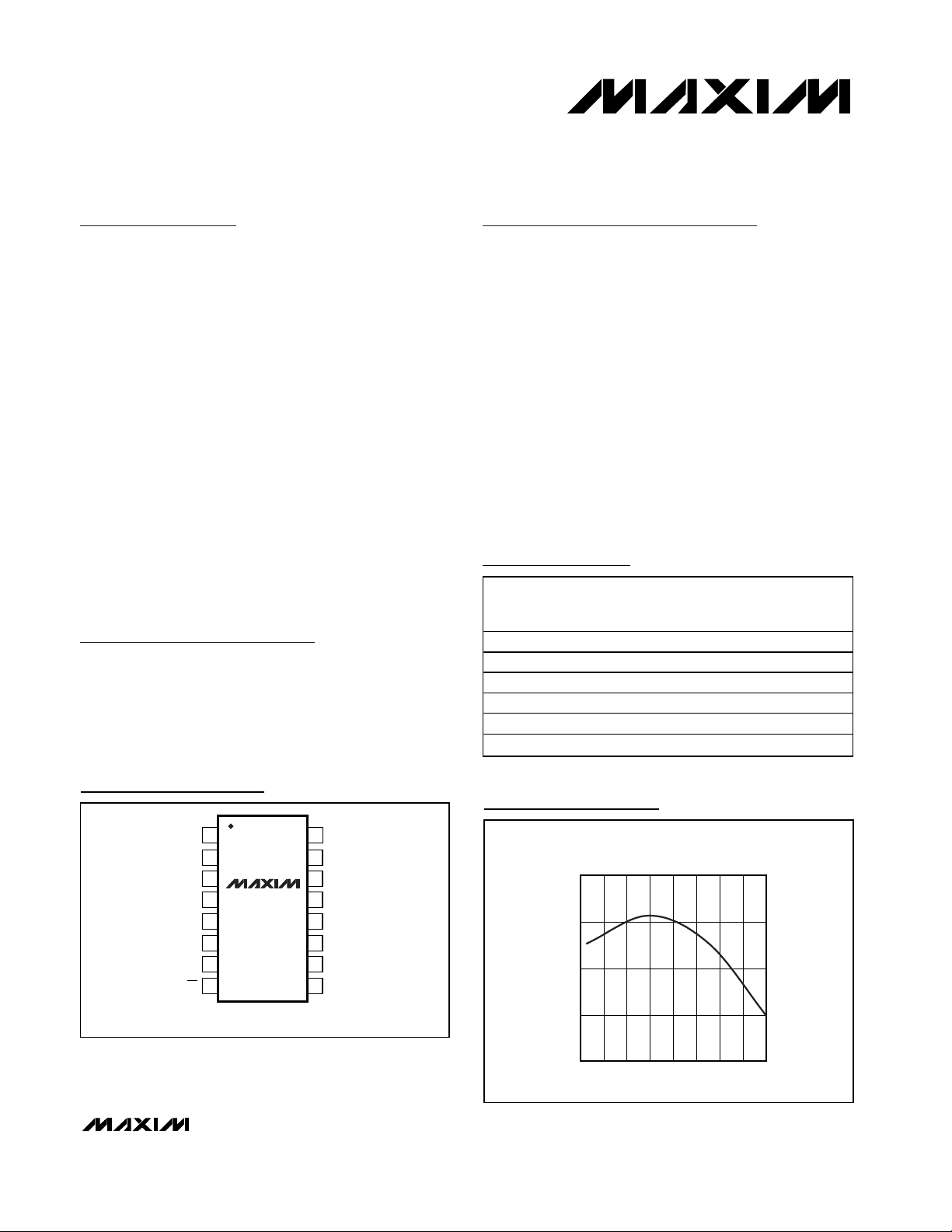
Pin Configuration
19-1728; Rev 0; 7/00
For free samples and the latest literature, visit www.maxim-ic.com or phone 1-800-998-8800.
For small orders, phone 1-800-835-8769.
Ordering Information
*Future product—contact factory for availability.
Typical Operating Circuit appears at end of data sheet.
SPI and QSPI are trademarks of Motorola, Inc.
MICROWIRE is a trademark of National Semiconductor Corp.
Temperature Error
TOP VIEW
1
AIN1 AIN0
SHO
2
AIN2
3
4
AIN3
AIN4
5
GND
6
SSTRB
7
CS
8
16
15
AIN5
14
REF
MAX1098
MAX1099
13
GND
12
V
DD
SCLK
11
DIN
10
COUT
9
PART
MAX1098AEAE* -40°C to +85°C 16 SSOP ±0.75
MAX1098BEAE* -40°C to +85°C 16 SSOP ±1.0
MAX1098CEAE -40°C to +85°C 16 SSOP ±4.0
MAX1099AEAE* -40°C to +85°C 16 SSOP ±0.75
MAX1099BEAE* -40°C to +85°C 16 SSOP ±1.0
MAX1099CEAE -40°C to +85°C 16 SSOP ±4.0
1.0
0.5
0
TEMP.
RANGE
TEMPERATURE ERROR
vs. INTERNAL DIODE TEMPERATURE
PIN PACKAGE
MAX1098
TEMP. SENSE
ACCURACY
MAX1098/9-29
(°C)
TEMPERATURE ERROR (°C)
SSOP
-0.5
-1.0
-60 -20 20 60-40 0 40 80 100
TEMPERATURE (°C)
Page 2
MAX1098/MAX1099
10-Bit Serial-Output Temperature Sensors
with 5-Channel ADC
2 _______________________________________________________________________________________
ABSOLUTE MAXIMUM RATINGS
ELECTRICAL CHARACTERISTICS
(VDD= +4.75V to +5.25V (MAX1098), VDD= +2.7V to +3.6V (MAX1099), external reference, V
REF
= +2.5V (MAX1098), V
REF
= +1.2V
(MAX1099), f
SCLK
= 2.5MHz, TA= T
MIN
to T
MAX
, unless otherwise noted. Typical values are at TA= +25°C.)
Stresses beyond those listed under “Absolute Maximum Ratings” may cause permanent damage to the device. These are stress ratings only, and functional
operation of the device at these or any other conditions beyond those indicated in the operational sections of the specifications is not implied. Exposure to
absolute maximum rating conditions for extended periods may affect device reliability.
VDDto GND.……………………………………………-0.3V to +6V
SHO to GND................................................-0.3V to (V
DD
+0.3V)
Analog Inputs to GND
(AIN0–AIN5, REF)...................................-0.3V to (V
DD
+0.3V)
Digital Inputs to GND (DIN, SCLK, CS).......-0.3V to (V
DD
+0.3V)
Digital Outputs to GND (DOUT, SSTRB) .....-0.3V to (V
DD
+0.3V)
Digital Output Sink Current ..…………………………………25mA
Maximum Current into Any Pin……………………………….50mA
Continuous Power Dissipation (T
A
= +70°C)
16-Pin SSOP (derate 8.00mW/°C above +70°C) ........667mW
Operating Temperature Range
MAX109_ _EAE...............................................-40°C to +85°C
Junction Temperature....……………………………………+150°C
Storage Temperature Range .............................-65°C to +150°C
Lead Temperature (soldering, 10s) .................................+300°C
DC ACCURACY (Note 1)
Resolution RES 10 Bits
Relative Accuracy (Note 2) INL ±1 LSB
Differential Nonlinearity DNL ±1 LSB
Offset Error Inputs AIN0−AIN5 ±1 LSB
Offset Temperature Coefficient ±10 µV/°C
Gain Error Inputs AIN0−AIN5, offset nulled ±1 LSB
VDD/4 Absolute Error ±1 LSB
Gain Temperature Coefficient ±2 ppm/°C
Channel-to-Channel Offset
Matching
CONVERSION RATE
Conversion Time (Note 3) t
Track/Hold Acquisition Time t
Aperture Delay t
Internal Clock Frequency f
ANALOG INPUTS (AIN0−AIN5)
Input Voltage Range (Note 4) Measurement with respect to IN-, Figure 1 -2V
Common-Mode Range 0V
Input Current (Note 5) 0.1 5 µA
Input Capacitance 16 pF
PARAMETER SYMBOL CONDITIONS MIN TYP MAX UNITS
CONV
ACQ
APR
CLK
Voltage measurement 1.1
Temperature measurement 2.2
±0.25 LSB
16 µs
30 ns
57.6 62.3 65.5 kHz
REF
+2V
REF
DD
ms
V
V
Page 3
MAX1098/MAX1099
10-Bit Serial-Output Temperature Sensors
with 5-Channel ADC
________________________________________________________________________________________ 3
ELECTRICAL CHARACTERISTICS (continued)
(VDD= +4.75V to +5.25V (MAX1098), VDD= +2.7V to +3.6V (MAX1099), external reference, V
REF
= +2.5V (MAX1098), V
REF
= +1.2V
(MAX1099), f
SCLK
= 2.5MHz, TA= T
MIN
to T
MAX
, unless otherwise noted. Typical values are at TA= +25°C.)
PARAMETER SYMBOL CONDITIONS MIN TYP MAX UNITS
DIGITAL INPUTS
Input Voltage Low V
Input Voltage High V
Input Hysteresis V
Input Leakage Current I
Input Capacitance 16 pF
DIGITAL OUTPUTS V
Output Low Voltage V
Output High Voltage V
Three-State Output Leakage
Current
Three-State Output
Capacitance
POWER REQUIREMENTS
Positive Supply Voltage V
Positive Supply Current
(Note 6)
Power-Supply Rejection
INTERNAL VOLTAGE REFERENCE CHARACTERISTICS
Reference Voltage V
Reference Tempco TC V
Output Short-Circuit Current 1.25 mA
Capacitive Bypass at REF 0.1 µF
REF Output Noise fN = 10Hz to 10kHz
REF Line Regulation
REF Load Regulation
IL
IH
HYST
IN
OL
OH
I
OUT
DD
I
DD
PSRR (Note 7) 50 65 dB
REF
REF
I
= 5mA 0.6 V
SINK
I
MAX1098 4.75 5.25
MAX1099 2.7 3.6
Full-on, voltage measurements,
internal reference
Full-on, voltage measurements,
external reference
Ful l - on, tem p er atur e m easur em ents,
i nter nal r efer ence
Ful l - on, tem p er atur e m easur em ents,
exter nal r efer ence
Standby, SCLK = GND 120
Standby-plus, SCLK = GND 190
Shutdown, SCLK = GND 2 10
VDD = 5V MAX1098
VDD = 3V MAX1099 1.197 1.20 1.203
0 to 100µA output current
(Note 8)
= 0.5mA V
SOURCE
MAX1098 390
MAX1099 350
MAX1098 310
MAX1099 280
MAX1098 440 500
MAX1099 400 500
MAX1098 360
MAX1099 330
MAX1098 130
MAX1099 65
MAX1098 +3.0
MAX1099 +0.2
MAX1098 4 10
MAX1099 2 10
V
- 0.8 V
D D
0.2 V
- 0.6 V
D D
15 pF
2.494 2.50 2.506
±20 ppm/°C
0.8 V
1 µA
±10 µA
V
µA
V
µV
RMS
mV/V
µV/µA
Page 4
MAX1098/MAX1099
10-Bit Serial-Output Temperature Sensors
with 5-Channel ADC
4 _______________________________________________________________________________________
ELECTRICAL CHARACTERISTICS (continued)
(VDD= 4.75V to 5.25V (MAX1098), VDD= 2.7V to 3.6V (MAX1099), external reference, V
REF
= +2.5V (MAX1098), V
REF
= +1.2V
(MAX1099), f
SCLK
= 2.5MHz, TA= T
MIN
to T
MAX
, unless otherwise noted. Typical values are at TA= +25°C.)
EXTERNAL VOLTAGE REFERENCE CHARACTERISTICS
Reference Voltage Range V
REF Input Resistance
REF Input Capacitance 24 pF
INTERNAL TEMPERATURE MEASUREMENT CHARACTERISTICS
Resolution 0.13 °C
Output Error (Notes 1, 9)
Power-Supply Rejection Ratio PSRR (Note 7) 0.2 °C/V
Noise 0.18 °C
EXTERNAL TEMPERATURE MEASUREMENT CHARACTERISTICS
Output Error 2N3904 (Note 10) ±2 ±4 °C
Remote Diode Excitation (1X) 10 µA
Remote Diode Excitation (10X) 100 µA
PARAMETER SYMBOL CONDITIONS MIN TYP MAX UNITS
REF
MAX1098 0.8 2.5
MAX1099 0.8 1.2
Converting 10
Shutdown 25
MAX109_A ±0.75
TA = +85°C, PD = 1mW
T
= -40°C to 0°C,
A
T
= +70°C to +85°C
A
MAX109_B ±1
MAX109_C ±1
MAX109_A
MAX109_B ±1TA = 0°C to +70°C
MAX109_C ±2
MAX109_A ±0.75
MAX109_B ±1
MAX109_C ±4
±0.75
V
MΩ
°C
RMS
Page 5
MAX1098/MAX1099
10-Bit Serial-Output Temperature Sensors
with 5-Channel ADC
________________________________________________________________________________________ 5
TIMING CHARACTERISTICS
(VDD= +4.75V to +5.25V (MAX1098), VDD= +2.7V to +3.6V (MAX1099), external reference, V
REF
= +2.5V (MAX1098), V
REF
= +1.2V
(MAX1099), f
SCLK
= 2.5MHz, TA= T
MIN
to T
MAX
, unless otherwise noted. Typical values are at TA= +25°C.) (Figures 4, 6)
Note 1: Tested at VDD= +5.0V (MAX1098) and VDD= +3.0V (MAX1099).
Note 2: Relative accuracy is the deviation of the analog value at any code from its theoretical value after the full-scale range has
been calibrated.
Note 3: Conversion time is defined as the number of clock cycles (64 for voltage measurements, 125 for temperature measure-
ments) multiplied by the internal clock period.
Note 4: Individual analog input voltages cannot extend beyond the power-supply rails.
Note 5: Input resistance is typically 250MΩ; 5µA limit reflects limitations in production testing.
Note 6: Specifications for full-on status assume continuous conversions. Power modes are software selected (Table 3).
Note 7: Measured at V
FS(+4.75V)
- V
FS(+5.25V)
for the MAX1098 and at V
FS(+2.7V)
- V
FS(+3.6V)
for the MAX1099.
Note 8: External load should not change during conversions for specified accuracy.
Note 9: Excludes noise and self-heating effects. Output error for MAX109_C guaranteed by design.
Note 10:External temperature sensing over -40°C to +85°C range, device at +25°C. Guaranteed by design.
SCLK Frequency f
SCLK Pulse Width Low t
SCLK Pulse Width High t
CS Low to SCLK High t
SCLK High to CS Setup t
CS Pulse Width t
SCLK High to CS Low Setup t
SCLK High to CS High Setup t
DIN Setup to SCLK High Time t
DIN Hold Time t
SCLK Fall to Output Data Valid t
CS Fall to Output Enable t
CS Rise to Output Disable t
SSTRB Rise to SCLK Rise t
SCLK Fall to SSTRB Fall t
PARAMETER SYMBOL CONDITIONS MIN TYP MAX UNITS
SCLK
CL
CH
CSS
CSH
CS
CS0
CS1
DS
DH
DO
DV
TR
SCLK
SSTRB
RL = 100kΩ, CL = 50pF 150 ns
RL = 100kΩ, CL = 50pF 150 ns
RL = 100kΩ, CL = 50pF 50 ns
200 ns
200 ns
100 ns
100 ns
100 ns
50 ns
100 ns
100 ns
0ns
0ns
200 ns
2.5 MHz
Page 6
MAX1098/MAX1099
10-Bit Serial-Output Temperature Sensors
with 5-Channel ADC
6 _______________________________________________________________________________________
Typical Operating Characteristics
(TA = +25°C, unless otherwise noted.)
-0.05
-0.10
-0.15
-0.20
0
0.05
0.10
0.15
0.20
-625 0 625
MAX1098
INTEGRAL NONLINEARITY
vs. OUTPUT CODE
MAX1098/9-01
OUTPUT CODE
INTEGRAL NONLINEARITY (LSB)
-625 0 625
MAX1099
INTEGRAL NONLINEARITY
vs. OUTPUT CODE
MAX1098/9-02
OUTPUT CODE
INTEGRAL NONLINEARITY (LSB)
-0.05
-0.10
-0.15
-0.20
0
0.05
0.10
0.15
0.20
-625 0 625
MAX1098
DIFFERENTIAL NONLINEARITY
vs. OUTPUT CODE
MAX1098/9-03
OUTPUT CODE
DIFFERENTIAL NONLINEARITY (LSB)
-0.05
-0.10
-0.15
-0.20
0
0.05
0.10
0.15
0.20
-625 0 625
MAX1099
DIFFERENTIAL NONLINEARITY
vs. OUTPUT CODE
MAX1098/9-04
OUTPUT CODE
DIFFERENTIAL NONLINEARITY (LSB)
-0.05
-0.10
-0.15
-0.20
0
0.05
0.10
0.15
0.20
0
150
100
50
200
250
300
350
400
450
500
4.7 4.94.8 5.0 5.1 5.2
MAX1098
SUPPLY CURRENT vs. SUPPLY VOLTAGE
(VOLTAGE MEASUREMENT MODE)
MAX1098/9-05
SUPPLY VOLTAGE (V)
SUPPLY CURRENT (µA)
EXTERNAL REFERENCE
INTERNAL REFERENCE
0
150
100
50
200
250
300
350
400
450
500
2.7 3.12.9 3.3 3.5
MAX1099
SUPPLY CURRENT vs. SUPPLY VOLTAGE
(VOLTAGE MEASUREMENT MODE)
MAX1098/9-06
SUPPLY VOLTAGE (V)
SUPPLY CURRENT (µA)
EXTERNAL REFERENCE
INTERNAL REFERENCE
0
150
100
50
200
250
300
350
400
450
500
4.7 4.94.8 5.0 5.1 5.2
MAX1098
SUPPLY CURRENT vs. SUPPLY VOLTAGE
(TEMPERATURE MEASUREMENT MODE)
MAX1098/9-07
SUPPLY VOLTAGE (V)
SUPPLY CURRENT (µA)
EXTERNAL REFERENCE
INTERNAL REFERENCE
0
150
100
50
200
250
300
350
400
450
500
2.7 3.12.9 3.3 3.5
MAX1099
SUPPLY CURRENT vs. SUPPLY VOLTAGE
(TEMPERATURE MEASUREMENT MODE)
MAX1098/9-08
SUPPLY VOLTAGE (V)
SUPPLY CURRENT (µA)
EXTERNAL REFERENCE
INTERNAL REFERENCE
0
150
100
50
250
200
450
400
350
300
500
-40 -20 0 20 40 60
80
MAX1098
SUPPLY CURRENT vs. TEMPERATURE
(VOLTAGE MEASUREMENT MODE)
MAX1098/9-09
TEMPERATURE (°C)
SUPPLY CURRENT (µA)
EXTERNAL REFERENCE
INTERNAL REFERENCE
Page 7

MAX1098/MAX1099
10-Bit Serial-Output Temperature Sensors
with 5-Channel ADC
_______________________________________________________________________________________ 7
Typical Operating Characteristics (continued)
(TA = +25°C, unless otherwise noted.)
0
150
100
50
250
200
450
400
350
300
500
-40 -20 0 20 40 60 80
MAX1099
SUPPLY CURRENT vs. TEMPERATURE
(VOLTAGE MEASUREMENT MODE)
MAX1098/9-10
TEMPERATURE (°C)
SUPPLY CURRENT (µA)
EXTERNAL REFERENCE
INTERNAL REFERENCE
0
150
100
50
250
200
450
400
350
300
500
-40 -20 0 20 40 60 80
MAX1098
SUPPLY CURRENT vs. TEMPERATURE
(TEMPERATURE MEASUREMENT MODE)
MAX1298/9-11
TEMPERATURE (°C)
SUPPLY CURRENT (µA)
EXTERNAL REFERENCE
INTERNAL REFERENCE
0
150
100
50
250
200
450
400
350
300
500
-40 -20 0 20 40 60 80
MAX1099
SUPPLY CURRENT vs. TEMPERATURE
(TEMPERATURE MEASUREMENT MODE)
MAX1098/9-12
TEMPERATURE (°C)
SUPPLY CURRENT (µA)
EXTERNAL REFERENCE
INTERNAL REFERENCE
0
150
100
50
200
250
300
350
400
450
500
4.7 4.94.8 5.0 5.1 5.2
MAX1098
POWER-DOWN SUPPLY CURRENT
vs. SUPPLY VOLTAGE
MAX1098/9-13
SUPPLY VOLTAGE (V)
SUPPLY CURRENT (µA)
STANDBY
STANDBY+
MAX1099
POWER-DOWN SUPPLY CURRENT
vs. SUPPLY VOLTAGE
0
150
100
50
200
250
300
350
400
450
500
2.7 3.12.9 3.3 3.5
MAX1098/9-14
SUPPLY VOLTAGE (V)
SUPPLY CURRENT (µA)
STANDBY
STANDBY+
0
150
100
50
250
200
450
400
350
300
500
-40 -20 0 20 40 60 80
MAX1098
POWER-DOWN SUPPLY CURRENT
vs. TEMPERATURE
MAX1098/9-15
TEMPERATURE (°C)
SUPPLY CURRENT (µA)
STANDBY
STANDBY+
0
150
100
50
250
200
450
400
350
300
500
-40 -20 0 20 40 60 80
MAX1099
POWER-DOWN SUPPLY CURRENT
vs. TEMPERATURE
MAX1098/9-16
TEMPERATURE (°C)
SUPPLY CURRENT (µA)
STANDBY
STANDBY+
2.52
2.51
2.50
2.49
2.48
4.7 5.04.8 4.9 5.1 5.2
MAX1098
INTERNAL REFERENCE VOLTAGE
vs. SUPPLY VOLTAGE
MAX1098/9-17
SUPPLY VOLTAGE (V)
REFERENCE VOLTAGE (V)
1.22
1.21
1.20
1.19
1.18
2.7 3.12.9 3.3 3.5
MAX1099
INTERNAL REFERENCE VOLTAGE
vs. SUPPLY VOLTAGE
MAX1098/9-18
SUPPLY VOLTAGE (V)
REFERENCE VOLTAGE (V)
Page 8

MAX1098/MAX1099
10-Bit Serial-Output Temperature Sensors
with 5-Channel ADC
8 _______________________________________________________________________________________
Typical Operating Characteristics (continued)
(TA = +25°C, unless otherwise noted.)
2.48
2.49
2.50
2.51
2.52
MAX1098
INTERNAL REFERENCE VOLTAGE
vs. TEMPERATURE
MAX1098/9-19
TEMPERATURE (°C)
REFERENCE VOLTAGE (V)
-40 20 40-20 0 60 80
1.18
1.19
1.20
1.21
1.22
MAX1099
INTERNAL REFERENCE VOLTAGE
vs. TEMPERATURE
MAX1098/9-20
TEMPERATURE (°C)
REFERENCE VOLTAGE (V)
-40 20 40-20 0 60 80
0.250
0.125
0
-0.125
-0.250
4.7 5.04.8 4.9 5.1 5.2
MAX1098
OFFSET vs. SUPPLY VOLTAGE
MAX1098/9-21
SUPPLY VOLTAGE (V)
OFFSET (LSB)
0.250
0.125
0
-0.125
-0.250
2.7 3.12.9 3.3 3.5
MAX1099
OFFSET vs. SUPPLY VOLTAGE
MAX1098/9-22
SUPPLY VOLTAGE (V)
OFFSET (LSB)
-0.250
-0.125
0
0.125
0.250
MAX1098
OFFSET vs. TEMPERATURE
MAX1098/9-23
TEMPERATURE (°C)
OFFSET (LSB)
-40 20 40-20 0 60 80
-0.250
-0.125
0
0.125
0.250
MAX1099
OFFSET vs. TEMPERATURE
MAX1098/9-24
TEMPERATURE (°C)
OFFSET (LSB)
-40 20 40-20 0 60 80
-0.25
0
0.25
MAX1098
GAIN ERROR vs. TEMPERATURE
MAX1098/9-27
TEMPERATURE (°C)
GAIN ERROR (LSB)
-40 20 40-20 0 60 80
-0.25
0
0.25
MAX1099
GAIN ERROR vs. TEMPERATURE
MAX1098/9-28
TEMPERATURE (°C)
GAIN ERROR (LSB)
-40 20 40-20 0 60 80
-1.0
-0.5
0
0.5
1.0
-60 -20 20 60-40 0 40 80 100
MAX1098
TEMPERATURE ERROR
vs. INTERNAL DIODE TEMPERATURE
MAX1098/9-29
TEMPERATURE (°C)
TEMPERATURE ERROR (°C)
Page 9

MAX1098/MAX1099
10-Bit Serial-Output Temperature Sensors
with 5-Channel ADC
________________________________________________________________________________________ 9
Typical Operating Characteristics (continued)
(TA= +25°C, unless otherwise noted.)
-1.0
-0.5
0
0.5
1.0
-60 -20 20 60-40 0 40 80 100
MAX1099
TEMPERATURE ERROR
vs. INTERNAL DIODE TEMPERATURE
MAX1098/9-30
TEMPERATURE (°C)
TEMPERATURE ERROR (°C)
-2.0
-1.0
-1.5
0
-0.5
0.5
1.0
1.5
2.0
-60 -20 0-40 20 40 60 80 100
MAX1098
TEMPERATURE ERROR
vs. REMOTE DIODE TEMPERATURE
MAX1098/9-31
TEMPERATURE (°C)
TEMPERATURE ERROR (°C)
-2.0
-1.0
-1.5
0
-0.5
0.5
1.0
1.5
2.0
-60 -20 0-40 20 40 60 80 100
MAX1099
TEMPERATURE ERROR
vs. REMOTE DIODE TEMPERATURE
MAX1098/9-32
TEMPERATURE (°C)
TEMPERATURE ERROR (°C)
Page 10

MAX1098/MAX1099
10-Bit Serial-Output Temperature Sensors
with 5-Channel ADC
10 ______________________________________________________________________________________
Pin Description
PIN NAME FUNCTION
1 AIN1
2 SHO
3 AIN2
4 AIN3
5 AIN4 Analog Input 4. Positive differential input relative to AIN5 (Table 4).
6 GND Ground. Connect to pin 13.
7 SSTRB
8 CS
9 DOUT Serial Data Output. DOUT transitions on the falling edge of SCLK.
10 DIN Serial Data Input. DIN latches data on the rising edge of SCLK.
11 SCLK Serial Clock Input. Clocks data in and out of the serial interface.
12 V
13 GND Ground (star ground)
14 REF
15 AIN5 Analog Input 5. Negative differential input relative to AIN0–AIN4 (Table 4).
16 AIN0
Analog Input 1. Negative differential input relative to AIN0 or positive differential input relative to AIN5
(Table 4). Connect to the cathode of external diode 1 for remote temperature sensing.
Shield Output. Used to suppress leakage currents at the anodes of remote temperature sensors (see Remote
Diode Shielding). May also be connected to the shields of twisted-pair input cables used for remote
temperature measurements. Leave unconnected for other applications.
Analog Input 2. Positive differential input relative to AIN3 or positive differential input relative to AIN5
(Table 4). Connect to the anode of external diode 2 for remote temperature sensing.
Analog Input 3. Negative differential input relative to AIN2 or positive differential input relative to AIN5
(Table 4). Connect to the cathode of external diode 2 for remote temperature sensing.
Serial Strobe Output. SSTRB goes low at the beginning of an A/D conversion, and it goes high when the
conversion is finished.
Active-Low Chip Select. Data will not be clocked into DIN unless CS is low. When CS is high, DOUT is at high
impedance.
Positive Supply Voltage. Bypass with a 0.1µF capacitor to GND (pin 13).
DD
Reference-Buffer Output/ADC Reference Input. Reference voltage for A/D conversion. Bypass to GND (pin 13)
with a 0.1µF capacitor. Select reference mode by writing to configuration byte (Table 1).
Analog Input 0. Positive differential input relative to AIN1 or positive differential input relative to AIN5
(Table 4). Connect to the anode of external diode 1 for remote temperature sensing.
Page 11

MAX1098/MAX1099
10-Bit Serial-Output Temperature Sensors
with 5-Channel ADC
_______________________________________________________________________________________ 11
Detailed Description
The MAX1098/MAX1099 are low-power, serial-output,
multichannel ADCs with temperature-sensing capability
for thermostatic, process-control, and monitoring applications. An algorithmic switched-capacitor converter
with T/H circuitry for both positive and negative inputs
supports fully differential 10-bit conversions from an
internal temperature sensor, two external temperature
sensors, or voltage sources in a variety of channel con-
figurations. Microprocessor (µP) control is made easy
through a flexible 3-wire serial interface.
Figure 1 shows a simplified functional diagram of the
MAX1098/MAX1099 internal architecture. In temperature-sensing mode, the multiplexer (mux) steers bias
currents through internal or external diodes while the
ADC computes their temperature in relation to changes
in forward voltage. Channels not used for temperature
measurement can be configured to measure other system voltages.
SCLK
Figure 1. MAX1098/MAX1099 Functional Diagram
CS
DIN
AIN0
AIN1
AIN2
AIN3
AIN4
AIN5
INPUT
REGISTER
DIODE
BIAS
CONTROL
INPUT
MUX
/4
V
DD
SHIELD
OUTPUT
T/H
T/H
CONTROL
LOGIC
+
IN
-
IN
ADC
OUTPUT
REGISTER
CLOCK
REF
DOUT
V
DD
GND
SHO REF
Page 12

MAX1098/MAX1099
10-Bit Serial-Output Temperature Sensors
with 5-Channel ADC
12 ______________________________________________________________________________________
Converter Operation
Figure 2 shows a simplified model of the converter
input structure. Once initiated, a voltage conversion
requires 64 f
CLK
periods, where f
CLK
is the internal
master clock. Each conversion is preceded by 13 f
CLK
periods of warm-up time, performed in twelve 4 f
CLK
period cycles, and followed by three f
CLK
periods to
load the output register. SSTRB falls at the beginning of
a conversion and rises at the end of a conversion.
Inputs IN+ and IN- charge capacitors C
HOLDP
and
C
HOLDN
, respectively, during the acquisition interval
that occurs during the first f
CLK
period of the first con-
version cycle. In the second f
CLK
period, the T/H
switches open so that charge is retained on C
HOLDP
and C
HOLDN
as a sample of the differential voltage
between IN+ and IN-. This charge is transferred to the
ADC during the third and fourth f
CLK
periods.
The reference sampling process begins in the second
conversion cycle and continues until the conversion is
complete. Sampling occurs during the second and
fourth f
CLK
periods to yield an effective doubling of the
reference voltage. The reference sampling requirement
is signal dependent and may or may not occur in every
subsequent conversion cycle.
Temperature conversion is nothing more than subtracting the results of two sequential voltage conversions. The
only difference is that output registers are not loaded at
the end of the first conversion. Thus, temperature conversions require 2 x 64 - 3 = 125 f
CLK
periods. Figures
3a and 3b show timing diagrams for voltage and temperature conversions, respectively.
Track/Hold
The T/H stage for the MAX1098/MAX1099 is a simple
switched-capacitor sampling operation. The time
required for the T/H stage to acquire an input signal is
a function of how fast its input capacitance is charged.
If the signal source impedance is high, the acquisition
time lengthens and more time must be allowed
between conversions. The acquisition time (t
ACQ
) is the
maximum time the device takes to acquire the signal.
Calculate this with the following equation:
t
ACQ
= 7 (Rs+ RIN) C
IN
where Rsis the source impedance of the input signal,
RINis the T/H input impedance (40kΩ), and CINis the
Figure 2. Converter Input Structure
TIMING/CONTROL
LOGIC
R
IN
IN+
IN-
TRACK AND HOLD
40k
R
40k
C
T/H
IN
T/H
HOLDP
4pF
C
HOLDN
4pF
FULLY
DIFFERENTIAL
A/D
R
R
REF
30k
C
4pF
REF
GAIN
OF 2
OUTPUT
Page 13

13 f
CLKs
WARMUP
44 f
CLKs
CONVERSION
CYCLES 2–12
REFERENCE
SAMPLING
3 f
CLKs
SUBTRACTION
AND WRITE TO
OUTPUT REGISTER
48 f
CLKs
CONVERSION CYCLES 1–12
13 f
CLKs
WARMUP
INPUT
ACQUISITION
INPUT
ACQUISITION
SSTRB
FCLK
4 f
CLKs
CONVERSION CYCLE 1
FIRST CONVERSION
SECOND CONVERSION
MAX1098/MAX1099
10-Bit Serial-Output Temperature Sensors
with 5-Channel ADC
_______________________________________________________________________________________ 13
input sampling capacitance of the ADC (4pF). Source
impedances below 100kΩ have no significant effect on
MAX1098/MAX1099 AC performance.
Analog Input Protection
Internal protection diodes clamp the analog inputs to
VDDand GND so channels can swing within GND -
0.3V and VDD+ 0.3V without damage. However, for
accurate conversions, the inputs should not extend
beyond the supply rails.
If an off-channel analog input extends beyond the
supply rails, limit the input current to 2mA.
Serial Digital Interface
The MAX1098/MAX1099 feature a serial interface that is
fully compatible with SPI, QSPI, and MICROWIRE
devices. For SPI/QSPI, ensure that the CPU serial interface runs in master mode so it generates the serial
clock signal. Select a 2.5MHz clock frequency or less,
and set zero values for clock polarity (CPOL) and
phase (CPHA) in the µP control registers. Figure 4
shows detailed serial interface timing information. See
Tables 1–4 for programming information.
13 f
CLKs
WARMUP
3 f
CLKs
WRITE TO OUTPUT
REGISTER
INPUT
ACQUISITION
F
CLKS
SSTRB
FCLK
REF
ACQUISITION 1
REF
ACQUISITION 2
CONVERSION CYCLE 1
CONVERSION CYCLES 2–12
REFERENCE SAMPLING
Figure 3b. Temperature Conversion Timing Diagram
Figure 3a. Voltage Conversion Timing Diagram
Page 14

MAX1098/MAX1099
10-Bit Serial-Output Temperature Sensors
with 5-Channel ADC
14 ______________________________________________________________________________________
Input Data Format
Input data (configuration and conversion bytes) are
clocked into the MAX1098/MAX1099 at DIN on the rising edge of SCLK when CS is low. The start bit (MSB)
of an input data byte is the first logic 1 bit that arrives:
After CS falls
OR
After receipt of a complete configuration byte with no
conversion in progress
OR
After 16 bits have been clocked onto DOUT following a
conversion.
Output Data Format
Output data from the MAX1098/MAX1099 are clocked
onto DOUT on the falling edge of SCLK in the form of two
8-bit words, MSB first (Table 5). For temperature conversions, the output is 12-bit binary (D8–S2) padded with 2
leading extraneous bits and two trailing zeros. For voltage conversions, the output is 10-bit two’s-complement
binary (D9–D0) with 3 sub-bits and two trailing zeros.
Figure 5 shows the bipolar transfer function.
Performing a Conversion
On power-up, the MAX1098/MAX1099 default to shutdown mode. Start a conversion by transferring a configuration byte and a conversion byte into DIN with the
control formats shown in Tables 1 and 2, respectively.
(See Power Modes for a related discussion.)
SSTRB goes low on the falling edge of the last bit of the
conversion byte, and it returns high when the conversion
is complete. For best noise performance, SCLK should
remain low while SSTRB is low. Typical conversion times
are 2.2ms for temperature measurements and 1.1ms for
voltage measurements. The MSB of the 2 output bytes is
present at DOUT starting at the rising edge of SSTRB.
Successive SCLK falling edges shift the two 8-bit data
bytes out from an internal register. Additional (>16)
SCLK edges will result in zeros on DOUT.
SSTRB does not go into a high-impedance state when
CS goes high. Pulling CS high prevents data from
being clocked in or out, but it does not adversely affect
a conversion in progress. Figure 6 shows SSTRB timing
details.
Subsequent conversions with the same reference mode
do not require a configuration byte.
Figure 4. Detailed Serial Interface Timing
Figure 5. Bipolar Transfer Function
CS
t
CS
t
CSS
t
CH
t
t
CL
DH
X
VALIDVALID VALID
t
DV
t
DO
t
CSH
t
CS1
X
t
TR
SCLK
DIN
DOUT
t
CS0
t
DS
X
OUTPUT CODE
0111111111
0111111110
0000000010
0000000001
0000000000
1111111111
1111111110
1111111101
1000000010
1000000001
+
FS
-
FS
1LSB =
-
FS + 1LSB
= +
2V
REF
= -
2V
REF
2V
REF
512
+
FS - 1LSB
IN
+ -
IN - (LSB)
0
Page 15

MAX1098/MAX1099
10-Bit Serial-Output Temperature Sensors
with 5-Channel ADC
_______________________________________________________________________________________ 15
Reference Selection
Select between internal and external voltage modes
through bit REF of the configuration byte. Set REF = 1
for internal reference mode and REF = 0 for external
reference mode.
Internal Reference
The MAX1098 has a 2.50V internal reference, while the
MAX1099 has a 1.20V internal reference. Both are factory trimmed for accuracy. When internal reference is
selected, REF can be used to drive an external load
with 100µA capability. Bypass REF to GND with a 0.1µF
minimum capacitance. Wake-up time is C x 2.5 x 10
4
s
for the MAX1098 and C x 1.2 x 10⁴s for the MAX1099.
External Reference
The MAX1098 can directly accept reference voltages at
REF from 0.8V to 2.5V, while the MAX1099 can directly
accept reference voltages from 0.8V to 1.2V. Bypass
REF to GND with a 0.1µF capacitor. Temperature measurements always use internal reference.
Power Modes
The MAX1098/(MAX1099) typically requires supply currents of 380µA (350µA) or 310µA (280µA) when performing voltage conversions at 100% duty cycle with
internal or external references, respectively. The differ-
Table 1. Configuration-Byte Format
Table 2. Conversion-Byte Format
Figure 6. Detailed SSTRB Timing
BIT 7
(MSB)
Start 0 0 0 0 PM1 PM0 REF
BIT NAME DESCRIPTION
7 (MSB) Start First logic 1 after CS goes low. (See Input Data Format.)
6, 5, 4, 3 Must be 0000 to load a configuration byte.
2, 1 PM1, PM0 These 2 bits select the desired power mode (Table 3).
0 REF
BIT 7
(MSB)
Start 0 1 0 SEL3 SEL2 SEL1 SEL0
BIT NAME DESCRIPTION
7 (MSB) Start First logic 1 after CS goes low. (See Input Data Format.)
6, 5, 4 Must be 010 to load a conversion byte.
3, 2, 1, 0
BIT 6 BIT 5 BIT 4 BIT 3 BIT 2 BIT 1
A logic high enables the internal reference. A logic low disables the internal reference and
selects the external reference mode.
BIT 6 BIT 5 BIT 4 BIT 3 BIT 2 BIT 1
SEL3, SEL2,
SEL1, SEL0
These 4 bits select the input configuration (Table 4).
BIT 0
(LSB)
BIT 0
(LSB)
CSB
t
CSH
SSTRB
SCLK
PDO CLOCKED IN
DOUT
t
CONV
t
SSTRB
SSTRB TIMING
t
SCK
t
t
CSS
DO
Page 16

MAX1098/MAX1099
10-Bit Serial-Output Temperature Sensors
with 5-Channel ADC
16 ______________________________________________________________________________________
ence reflects the power requirement of an internal reference buffer amplifier that can accommodate external
loads. Temperature conversions at 100% duty cycle
increase supply currents to 440µA (400µA) through
additional amplification, buffer, and bias circuitry that is
otherwise inactive.
Place the MAX1098/MAX1099 in a low-current powerdown state between conversions to conserve power.
Select standby, standby plus, or shutdown through bits
PM1 and PM0 of the initialization byte (Table 3).
The MAX1098/MAX1099 assume the shutdown power
mode when VDDis first applied.
Standby Mode
Standby mode turns off the MAX1098/MAX1099 ADC,
internal clock, and reference buffer amplifier. Special
circuitry for temperature conversions is also deactivated. Wake-up time is limited by the reference buffer
amplifier and the associated bypass capacitor (see
Internal Reference). When an external reference is
used, wake-up time is 0.1ms.
Standby-Plus Mode
Standby-plus mode is similar to the standby mode, but
the internal reference output buffer remains active to
shorten the wake-up time to 0.1ms for internal reference mode. When using an external reference, standby-plus mode is equivalent to standby mode.
Shutdown Mode
Shutdown mode turns off all functions other than startup circuitry, thereby reducing typical supply current to
2µA. Data registers are cleared. Use this power mode
when interconversion times are no less than 5ms.
Monitoring V
DD
This mode of operation samples and converts the supply voltage, V
DD
/4, which is internally generated. The
reference voltage must be larger than V
DD
/8 for the
operation to work properly. From the result of a conversion (CODE), CODE = 64 VDD/ V
REF
.
Temperature Measurements
The MAX1098/MAX1099 perform temperature measurements with internal or external diode-connected transistors through a three-step process. First, the diode bias
current changes from 31.6µA to 10µA to produce a
temperature-dependent bias voltage difference, which
is amplified by a factor of 20 and converted to digital
format. Second, the bias current changes from 31.6µA
to 100µA, and the bias voltage difference is similarly
amplified by a factor of 20 and converted to digital format. Third, the intermediate results are subtracted to
achieve a digital output that is proportional to absolute
temperature in degrees Kelvin.
The reference voltage used in conjunction with temperature measurements is derived from the internal reference
source to ensure that 1LSB corresponds to 1/8 of a
degree. To convert to degrees Celsius, subtract 273.15
from the temperature inferred from the ADC output.
Temperature measurements require a conversion time
of 2.2ms.
Shield Output Buffer
The MAX1098/MAX1099 provide a shield output buffer
voltage at SHO that is approximately 0.6V (one diode
drop) above VDD/2. When performing temperature
measurements with an external diode, use this voltage
to suppress error-producing leakage currents (see
Remote Diode Shielding). Figure 7 shows the SHO output circuit.
Applications Information
Remote Diode Selection
Temperature accuracy depends on having a goodquality, diode-connected, small-signal transistor.
Accuracy has been experimentally verified for 2N3904
devices. CPUs and other ICs having on-board temperature-sensing diodes can also be monitored if the
diode connections are floating.
Table 3. Power-Mode Selection
See Power Requirements in Electrical Characteristics.
Figure 7. SHO Output Circuit
PM1 PM0 MODE
0 0 Shutdown
0 1 Standby plus
1 0 Standby
1 1 Normal operation
5
µA
V
DD
2
SHO
Page 17

The transistor must be a small-signal type with a base
resistance less than 100Ω. Tight specifications for forward current gain (+50 to +150, for example) indicate
that the manufacturer has good process controls and
that the devices have consistent V
be
characteristics.
(See Table 6 for recommended devices.)
For heatsink mounting, the 500-32BT02-000 thermal
sensor from Fenwal Electronics is a good choice. This
device consists of a diode-connected transistor, an aluminum plate with screw hole, and twisted-pair cable
(Fenwal Inc., Milford MA, 508-478-6000).
Twisted-Pair and Shielded Cables
For remote-sensor distances greater than 8 inches, or
in particularly noisy environments, use a twisted-pair
cable. A practical length is 6 feet to 12 feet. For longer
distances, the best solution is a shielded twisted-pair
cable such as that used for audio microphones. For
MAX1098/MAX1099
10-Bit Serial-Output Temperature Sensors
with 5-Channel ADC
_______________________________________________________________________________________ 17
*Temperature-measurement mode
Table 4. Input Selection
Table 6. Remote-Sensor Transistor
Manufacturers
Table 5. Output Data Format
SEL3 SEL2 SEL1 SEL0 POSITIVE INPUT (IN+) NEGATIVE INPUT (IN-)
0000 AIN0 AIN5
0001 AIN1 AIN5
0010 AIN2 AIN5
0011 AIN3 AIN5
0100 AIN4 AIN5
0101 ——
0110 AIN5 AIN5
0111 Internal diode anode* Internal diode cathode
1000 AIN0 AIN1
1001 AIN2 AIN3
1010 ——
1011 V
1100 External diode 1 anode* (AIN0) External diode 1 cathode (AIN1)
1101 External diode 2 anode* (AIN2) External diode 2 cathode (AIN3)
1110 ——
1111 ——
/4 GND
DD
D9 D9 D8 D7 D6 D5 D4 D3 D2 D1 D0 S0 S 1S 200
MANUFACTURER MODEL NUMBER
Central Semiconductor
(USA)
Fairchild Semiconductor
(USA)
Motorola (USA) MMBT3904
Rohm Semiconductor
(Japan)
Siemens (Germany) SMB3904
Zetex (England) FMMT3904CT-ND
CMPT3904
MMBT3904
SST3904
Page 18

MAX1098/MAX1099
example, the Belden 8451 works well for distances up
to 100 feet in a noisy environment. Connect the shield
to SH0-0H.
Cable resistances affect remote-sensor accuracy; 1Ω
series resistance introduces +0.45°C error.
Remote Diode Shielding
Temperature measurements will reflect significant error
if a portion of the bias current supplied to the diode
anode is allowed to flow through parallel paths to
ground. If the diode-connected transistor is mounted
on a PC board, suppress error-producing “leakage”
current by surrounding the collector/base leads with a
metal trace that is connected to the SHO shield output
(Figure 8).
Layout, Grounding, and Bypassing
For best performance, use PC boards. Do not use wirewrap boards. Board layout should ensure that digital
and analog signal lines are separated from each other.
Do not run analog and digital (especially clock) signals
parallel to one another or run digital lines underneath
the ADC package.
High-frequency noise in the VDDpower supply may
affect ADC performance. Bypass the supply with a
0.1µF capacitor close to pin VDD. Minimize capacitor
lead lengths for best supply-noise rejection. If the
power supply is very noisy, connect a 10Ω resistor in
series with the supply to provide lowpass filtering.
Definitions
Relative Accuracy
Relative accuracy is the deviation of the values on an
actual transfer function from a straight line. This straight
line can be either a best-straight-line fit or a line drawn
between the endpoints of the transfer function, once
offset and gain errors have been nullified. The static linearity parameters for the MAX1098/MAX1099 are measured using the best-straight-line fit method.
Differential Nonlinearity (DNL)
Differential nonlinearity is the difference between an
actual step width and the ideal value of 1LSB. A DNL
error specification of less than 1LSB guarantees no
missing codes and a monotonic transfer function.
Offset Error
Offset error is the difference between the ideal and the
actual offset points. For an ADC, the offset point is the
midstep value when the digital output is zero.
Gain Error
Gain or full-scale error is the difference between the
ideal and actual gain points on the transfer function,
after the offset error has been canceled out. For an
ADC, the gain point is the midstep value when the digital output is full scale.
Aperture Delay
Aperture delay (tAD) is the time defined between the
rising edge of the sampling clock and the instant when
an actual sample is taken.
Chip Information
TRANSISTOR COUNT: 13,669
PROCESS: BiCMOS
10-Bit Serial-Output Temperature Sensors
with 5-Channel ADC
18 ______________________________________________________________________________________
Figure 8. Remote Diode Shielding for PC Boards
SHIELD
ANODE
CATHODE
Page 19
MAX1098/MAX1099
10-Bit Serial-Output Temperature Sensors
with 5-Channel ADC
_______________________________________________________________________________________ 19
Typical Operating Circuit
2N3904
2N3904
(SHIELD)
0.1µF
AIN0
AIN1
AIN2
AIN3
SHO
AIN4
AIN5
+5V
V
DD
MAX1098
GND GND
CS
SCLK
DIN
DOUT
SSTRB
Page 20

MAX1098/MAX1099
10-Bit Serial-Output Temperature Sensors
with 5-Channel ADC
Maxim cannot assume responsibility for use of any circuitry other than circuitry entirely embodied in a Maxim product. No circuit patent licenses are
implied. Maxim reserves the right to change the circuitry and specifications without notice at any time.
20 ____________________Maxim Integrated Products, 120 San Gabriel Drive, Sunnyvale, CA 94086 408-737-7600
© 2000 Maxim Integrated Products Printed USA is a registered trademark of Maxim Integrated Products.
Package Information
SSOP.EPS
 Loading...