

Page 1
General Description
The MAX109, 2.2Gsps, 8-bit, analog-to-digital converter
(ADC) enables the accurate digitizing of analog signals
with frequencies up to 2.5GHz. Fabricated on an
advanced SiGe process, the MAX109 integrates a highperformance track/hold (T/H) amplifier, a quantizer, and
a 1:4 demultiplexer on a single monolithic die. The
MAX109 also features adjustable offset, full-scale voltage (via REFIN), and sampling instance allowing multiple ADCs to be interleaved in time.
The innovative design of the internal T/H amplifier,
which has a wide 2.8GHz full-power bandwidth,
enables a flat-frequency response through the second
Nyquist region. This results in excellent ENOB performance of 6.9 bits. A fully differential comparator design
and decoding circuitry reduce out-of-sequence code
errors (thermometer bubbles or sparkle codes) and
provide excellent metastability performance (10
14
clock
cycles). This design guarantees no missing codes.
The analog input is designed for both differential and
single-ended use with a 500mV
P-P
input-voltage range.
The output data is in standard LVDS format, and is
demultiplexed by an internal 1:4 demultiplexer. The
LVDS outputs operate from a supply-voltage range of
3V to 3.6V for compatibility with single 3V-reference
systems. Control inputs are provided for interleaving
additional MAX109 devices to increase the effective
system-sampling rate.
The MAX109 is offered in a 256-pin Super Ball-Grid Array
(SBGA) package and is specified over the extended
industrial temperature range (-40°C to +85°C).
Applications
Radar Warning Receivers (RWR)
Light Detection and Ranging (LIDAR)
Digital RF/IF Signal Processing
Electronic Warfare (EW) Systems
High-Speed Data-Acquisition Systems
Digital Oscilloscopes
High-Energy Physics Instrumentation
ATE Systems
Features
♦ Ultra-High-Speed, 8-Bit, 2.2Gsps ADC
♦ 2.8GHz Full-Power Analog Input Bandwidth
♦ Excellent Signal-to-Noise Performance
44.6dB SNR at f
IN
= 300MHz
44dB SNR at fIN= 1600MHz
♦ Superior Dynamic Range at High-IF
61.7dBc SFDR at f
IN
= 300MHz
50.3dBc SFDR at f
IN
= 1600MHz
-60dBc IM3 at f
IN1
= 1590MHz and f
IN2
= 1610MHz
♦ 500mV
P-P
Differential Analog Inputs
♦ 6.8W Typical Power Including the Demultiplexer
♦ Adjustable Range for Offset, Full-Scale, and
Sampling Instance
♦ 50Ω Differential Analog Inputs
♦ 1:4 Demultiplexed LVDS Outputs
♦ Interfaces Directly to Common FPGAs with DDR
and QDR Modes
MAX109
8-Bit, 2.2Gsps ADC with Track/Hold Amplifier
and 1:4 Demultiplexed LVDS Outputs
________________________________________________________________
Maxim Integrated Products
1
Ordering Information
19-0795; Rev 0; 4/07
For pricing, delivery, and ordering information, please contact Maxim/Dallas Direct! at
1-888-629-4642, or visit Maxim’s website at www.maxim-ic.com.
D = Dry pack.
EVALUATION KIT
AVAILABLE
Pin Configuration
PART TEMP RANGE
MAX109EHF-D -40°C to +85°C 256 SBGA H256-1
TOP VIEW
1234567891011121314151617181920
A
B
C
D
E
F
G
H
J
K
L
M
N
P
R
T
U
V
W
Y
PINPACKAGE
MAX109
256-PIN
SBGA PACKAGE
256-PIN SUPER BALL-GRID ARRAY
PKG
CODE
Page 2
MAX109
8-Bit, 2.2Gsps ADC with Track/Hold Amplifier
and 1:4 Demultiplexed LVDS Outputs
2 _______________________________________________________________________________________
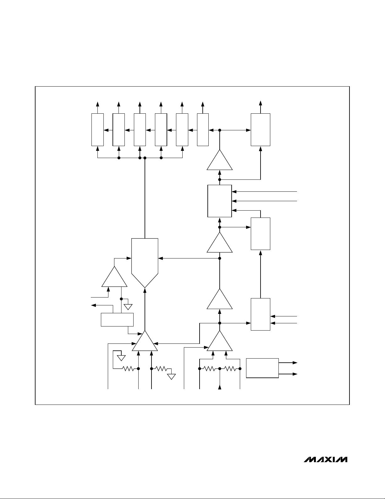
Figure 1. Functional Diagram of the MAX109
RSTOUTA[0:7] B[0:7] C[0:7] D[0:7] DOR DCO
DEMUX
PORTA
PORTB
PORTC
PORTD
DOR
DCO
RESET
OUTPUT
REFIN
REFOUT
REFERENCE
AMPLIFIER
BANDGAP
REFERENCE
8-BIT
ADC
CORE
T/H AMPLIFIER
DEMUX
CLOCK
GENERATOR
DEMUX
CLOCK
DRIVER
LOGIC
CLOCK
DRIVER
QUANTIZER
CLOCK
DRIVER
DELAYED
RESET
RESET
PIPELINE
RESET
INPUT
DUAL
LATCH
QDR
DDR
RSTINN
RSTINP
INPUT CLOCK BUFFER
50Ω50Ω 50Ω
VOSADJ CLKP CLKCOM
SAMPADJINP INN
50Ω
TEMPERATURE
MONITOR
CLKN
GNDI
TEMPMON
Page 3
MAX109
ABSOLUTE MAXIMUM RATINGS
DC ELECTRICAL CHARACTERISTICS
(VCCA = VCCI = VCCD = 5V, VCCO = 3.3V, V
EE
= -5V, GNDA = GNDI = GNDO = GNDD = GNDR = 0V, VOSADJ = SAMPADJ =
open, digital output pins differential R
L
= 100Ω. Specifications ≥ +25°C guaranteed by production test, < +25°C guaranteed by
design and characterization. Typical values are at T
A
= +25°C, unless otherwise noted.)
Stresses beyond those listed under “Absolute Maximum Ratings” may cause permanent damage to the device. These are stress ratings only, and functional
operation of the device at these or any other conditions beyond those indicated in the operational sections of the specifications is not implied. Exposure to
absolute maximum rating conditions for extended periods may affect device reliability.
VCCA to GNDA ....................................................... -0.3V to +6V
V
CC
D to GNDD ....................................................... -0.3V to +6V
V
CC
I to GNDI........................................................... -0.3V to +6V
V
CC
O to GNDO ................................................... -0.3V to +3.9V
V
EE
to GNDI ............................................................ -6V to +0.3V
Between Grounds (GNDA, GNDI, GNDO,
GNDD, GNDR) ................................................ -0.3V to +0.3V
V
CC
A to VCCD ..................................................... -0.3V to +0.3V
V
CC
A to VCCI ....................................................... -0.3V to +0.3V
Differential Voltage between INP and INN ........................... ±1V
INP, INN to GNDI ................................................................. ±1V
Differential Voltage between CLKP and CLKN..................... ±3V
CLKP, CLKN, CLKCOM to GNDI ............................... -3V to +1V
Digital LVDS Outputs to GNDO .............. -0.3V to (V
CC
O - 0.3V)
REFIN, REFOUT to GNDR ........................-0.3V to (V
CC
I + 0.3V)
REFOUT Current ...............................................-100µA to +5mA
RSTINP, RSTINN to GNDA .....................-0.3V to (V
CC
O + 0.3V)
RSTOUTP, RSTOUTN to GNDO .............-0.3V to (V
CC
O + 0.3V)
VOSADJ, SAMPADJ,
TEMPMON to GNDI...............................-0.3V to (V
CC
I + 0.3V)
PRN, DDR, QDR to GNDD.......................-0.3V to (V
CC
D + 0.3V)
DELGATE0, DELGATE1 to GNDA ...........-0.3V to (V
CC
A + 0.3V)
Continuous Power Dissipation (T
A
= +70°C)
256-Ball SBGA (derate 74.1mW/°C above +70°C for
a multilayer board) ................................................. 5925.9mW
Operating Temperature Range
MAX109EHF ...................................................-40°C to +85°C
Thermal Resistance θ
JA
(Note 1) .......................................3°C/W
Operating Junction Temperature.....................................+150°C
Storage Temperature Range .............................-65°C to +150°C
8-Bit, 2.2Gsps ADC with Track/Hold Amplifier
and 1:4 Demultiplexed LVDS Outputs
_______________________________________________________________________________________ 3
Note 1: Thermal resistance is based on a 5in x 5in multilayer board. The data sheet assumes a thermal environment of 3°C/W.
Thermal resistance may be different depending on airflow and heatsink cooling capabilities.
DC ACCURACY
Resolution RES 8 Bits
Integral Nonlinearity (Note 2) INL (Note 8) -0.8 ±0.25 +0.8 LSB
Differential Nonlinearity (Note 2) DNL
Transfer Curve Offset (Note 2) V
ANALOG INPUTS (INN, INP)
Common-Mode Input-Voltage
Range
Common-Mode Rejection Ratio
(Note 3)
Full-Scale Input Range (Note 2) V
Input Resistance R
Input Resistance Temperature
Coefficient
VOS ADJUST CONTROL INPUT (VOSADJ)
Input Resistance (Note 4) R
Input Offset Voltage V
SAMPLE ADJUST CONTROL INPUT (SAMPADJ)
Input Resistance R
Aperture Time Adjust Range t
PARAMETER SYMBOL CONDITIONS MIN TYP MAX UNITS
SAMPADJ
Guaranteed no missing codes, T
(Note 8)
OS
V
CM
CMRR 50 dB
TC
VOSADJ
OS
AD
VOSADJ control input open (Note 8) -5.5 0 +5.5 LSB
Signal and offset with respect to GNDI ±1 V
V
FS
IN
R
= 2.5V 470 500 535 mV
REFIN
VOSADJ = 0V -20 mV
VOSADJ = 2.5V 20 mV
SAMPADJ = 0 to 2.5V 30 ps
= +25°C
A
-0.8 ±0.25 +0.8 LSB
45 50 55 Ω
150 ppm/°C
25 50 75 kΩ
25 50 75 kΩ
P-P
Page 4
MAX109
8-Bit, 2.2Gsps ADC with Track/Hold Amplifier
and 1:4 Demultiplexed LVDS Outputs
4 _______________________________________________________________________________________
DC ELECTRICAL CHARACTERISTICS (continued)
(VCCA = VCCI = VCCD = 5V, VCCO = 3.3V, V
EE
= -5V, GNDA = GNDI = GNDO = GNDD = GNDR = 0V, VOSADJ = SAMPADJ =
open, digital output pins differential R
L
= 100Ω. Specifications ≥ +25°C guaranteed by production test, < +25°C guaranteed by
design and characterization. Typical values are at T
A
= +25°C, unless otherwise noted.)
REFERENCE INPUT AND OUTPUT (REFIN, REFOUT)
Reference Output Voltage REFOUT 2.460 2.500 2.525 V
Reference Output Load
Regulation
Reference Input Voltage REFIN
Reference Input Resistance R
CLOCK INPUTS (CLKP, CLKN)
Clock Input Amplitude Peak-to-peak differential (Figure 13b)
Clock Input Common-Mode
Range
Clock Input Resistance R
Input Resistance Temperature
Coefficient
CMOS CONTROL INPUTS (DDR, QDR, PRN, DELGATE0, DELGATE1)
High-Level Input Voltage V
Low-Level Input Voltage V
High-Level Input Current I
Low-Level Input Current I
LVDS INPUTS (RSTINP, RSTINN)
Differential Input High Voltage 0.2 V
Differential Input Low Voltage -0.2 V
Minimum Common-Mode Input
Voltage
Maximum Common-Mode Input
Voltage
TEMPERATURE MEASUREMENT OUTPUT (TEMPMON)
Temperature Measurement
Accuracy
Output Resistance Measured between TEMPMON and GNDI 0.725 kΩ
LVDS OUTPUTS (PortA, PortB, PortC, PortD, DORP, DORN, DCOP, DCON, RSTOUTP, RSTOUTN) (Note 9)
Differential Output Voltage V
Output Offset Voltage V
PARAMETER SYMBOL CONDITIONS MIN TYP MAX UNITS
∆REFOUT 0 < I
< 2.5mA < 7.5 mV
SOURCE
REFIN
CLK
TC
R
IH
IL
IH
IL
OD
OS
Signal and offset referenced to CLKCOM -2 to +2 V
CLKP and CLKN to CLKCOM 45 50 55 Ω
Threshold voltage = 1.2V 1.4 3.3 V
Threshold voltage = 1.2V 0.8 V
V
= 3.3V 50 µA
IH
V
= 0V -50 µA
IL
T (°C) = [(V
371
R
LOAD
R
LOAD
TEMPMON
= 100Ω 250 400 mV
= 100Ω 1.10 1.28 V
- V
GNDI
) x 1303.5] -
45 kΩ
V
2.500
± 0.25
200 to
2000
150 ppm/°C
1V
O -
C C
0.15
±7 °C
V
mV
V
Page 5
MAX109
8-Bit, 2.2Gsps ADC with Track/Hold Amplifier
and 1:4 Demultiplexed LVDS Outputs
_______________________________________________________________________________________ 5
DC ELECTRICAL CHARACTERISTICS (continued)
(VCCA = VCCI = VCCD = 5V, VCCO = 3.3V, V
EE
= -5V, GNDA = GNDI = GNDO = GNDD = GNDR = 0V, VOSADJ = SAMPADJ =
open, digital output pins differential R
L
= 100Ω. Specifications ≥ +25°C guaranteed by production test, < +25°C guaranteed by
design and characterization. Typical values are at T
A
= +25°C, unless otherwise noted.)
AC ELECTRICAL CHARACTERISTICS
(VCCA = VCCI = VCCD = 5V, VCCO = 3.3V, VEE= -5V, GNDA = GNDI = GNDD = GNDO = GNDR = 0V, f
CLK
= 2.2Gsps, analog input
amplitude at -1dBFS differential, clock input amplitude 400mV
P-P
differential, digital output pins differential RL= 100Ω. Typical values
are at T
A
= +25°C, unless otherwise noted.)
POWER REQUIREMENTS
Analog Supply Current IVCCA 556 744 mA
Positive Input Supply Current IVCCI 125 168 mA
Negative Input Supply Current IIV
Digital Supply Current IVCCD 291 408 mA
Output Supply Current IVCCO 222 300 mA
Power Dissipation P
Positive Power-Supply Rejection
Ratio
Negative Power-Supply Rejection
Ratio
PARAMETER SYMBOL CONDITIONS MIN TYP MAX UNITS
PSRRP (Note 5) 50 dB
PSRRN V
I 181 240 mA
EE
DISS
= -5.25V to -4.75V 50 dB
EE
6.50 8.79 W
PARAMETER SYMBOL CONDITIONS MIN TYP MAX UNITS
ANALOG INPUT
Analog Input Full-Power
Bandwidth (Note 6)
Gain Flatness GF 1100MHz to 2200MHz ±0.3 dB
DYNAMIC SPECIFICATIONS
Signal-to-Noise Ratio
Total H ar m oni c D i st or ti on ( N ote 7)
BW
SNR
SNR
SNR
SNR
SNR
SNR
THD
THD
THD
THD
THD
THD
-3dB
300fIN
1000fIN
1600fIN
2500fIN
500fIN
1600fIN
300fIN
1000fIN
1600fIN
2500fIN
500fIN
1600fIN
= 300MHz, f
= 1000MHz, f
= 1600MHz, f
= 2500MHz, f
= 500MHz, f
= 1600MHz, f
= 300MHz, f
= 1000MHz, f
= 1600MHz, f
= 2500MHz, f
= 500MHz, f
= 1600MHz, f
= 2.2Gsps 44.6
CLK
= 2.2Gsps (Note 8) 43.6 44.5
CLK
= 2.2Gsps (Note 8) 42.2 44.0
CLK
= 2.2Gsps 42.9
CLK
= 2.5Gsps 44.4
CLK
= 2.5Gsps 44.0
CLK
= 2.2Gsps -55.6
CLK
= 2.2Gsps (Note 8) -48.5 -42.5
CLK
= 2.2Gsps (Note 8) -46.6 -39.6
CLK
= 2.2Gsps -43.7
CLK
= 2.5Gsps -49.0
CLK
= 2.5Gsps -43.1
CLK
2.8 GHz
dB
dBc
Page 6
MAX109
8-Bit, 2.2Gsps ADC with Track/Hold Amplifier
and 1:4 Demultiplexed LVDS Outputs
6 _______________________________________________________________________________________
AC ELECTRICAL CHARACTERISTICS (continued)
(VCCA = VCCI = VCCD = 5V, VCCO = 3.3V, VEE= -5V, GNDA = GNDI = GNDD = GNDO = GNDR = 0V, f
CLK
= 2.2Gsps, analog input
amplitude at -1dBFS differential, clock input amplitude 400mV
P-P
differential, digital output pins differential RL= 100Ω. Typical values
are at T
A
= +25°C, unless otherwise noted.)
)
PARAMETER SYMBOL CONDITIONS MIN TYP MAX UNITS
Spurious Free Dynamic Range
Signal-to-Noise-Plus-Distortion
Ratio
SFDR
SFDR
SFDR
SFDR
SFDR
SFDR
SINAD
SINAD
SINAD
SINAD
SINAD
SINAD
300fIN
1000fIN
1600fIN
2500fIN
500fIN
1600fIN
300fIN
1000fIN
1600fIN
2500fIN
500fIN
1600fIN
Third-Order Intermodulation IM3 f
= 300MHz, f
= 1000MHz, f
= 1600MHz, f
= 2500MHz, f
= 500MHz, f
= 1600MHz, f
= 300MHz, f
= 1000MHz, f
= 1600MHz, f
= 2500MHz, f
= 500MHz, f
= 1600MHz, f
= 1590MHz, f
IN1
= 2.2Gsps 61.7
CLK
= 2.2Gsps (Note 8) 44.4 51.1
CLK
= 2.2Gsps (Note 8) 43.7 50.3
CLK
= 2.2Gsps 45.0
CLK
= 2.5Gsps 53.7
CLK
= 2.5Gsps 44.6
CLK
= 2.2Gsps 44.1
CLK
= 2.2Gsps (Note 8) 40.4 43.1
CLK
= 2.2Gsps (Note 8) 37.9 42.1
CLK
= 2.2Gsps 40.1
CLK
= 2.5Gsps 43.1
CLK
= 2.5Gsps 40.5
CLK
= 1610MHz at -7dBFS -60 dBc
IN2
Metastability Probability 10
TIMING CHARACTERISTICS
Maximum Sample Rate f
Clock Pulse-Width Low t
Clock Pulse-Width High t
Aperture Delay t
Aperture Jitter t
Reset Input Data Setup Time t
Reset Input Data Hold Time t
CLK-to-DCO Propagation Delay
DCO-to-Data Propagation Delay
CLK(MAX
PWL
PWH
AD
AJ
SU
HD
t
PD1
t
PD1DDR
t
PD1QDR
t
PD2
t
PD2DDR
t
PD2QDR
t
= t
+ t
CLK
t
CLK
= t
PWL
PWL
(Note 8) 180 ps
PWH
+ t
(Note 8) 180 ps
PWH
(Note 8) 300 ps
(Note 8) 250 ps
DCO = f
DCO = f
/ 4, CLK fall to DCO rise time 1.6
CLK
/ 8, DDR mode, CLK fall to
CLK
DCO rise time
DCO = f
/ 16, QDR mode, CLK fall to
CLK
DCO rise time
DCO = f
/ 4, DCO rise to data transition
CLK
(Note 8)
DCO = f
/ 8, DDR mode, DCO rise to
CLK
data transition (Note 8)
DCO = f
/ 16, QDR mode, DCO rise to
CLK
data transition (Note 8)
DCO Duty Cycle Clock mode independent
2.2 Gsps
-520 +520
-520 +
2t
CLK
-520 +
2t
CLK
dBc
dB
-14
200 ps
0.2 ps
1.6
ns
1.6
CLK
CLK
55
520 +
2t
CLK
520 +
2t
CLK
ps
%
2t
2t
45 to
Page 7
MAX109
8-Bit, 2.2Gsps ADC with Track/Hold Amplifier
and 1:4 Demultiplexed LVDS Outputs
_______________________________________________________________________________________ 7
AC ELECTRICAL CHARACTERISTICS (continued)
(VCCA = VCCI = VCCD = 5V, VCCO = 3.3V, VEE= -5V, GNDA = GNDI = GNDD = GNDO = GNDR = 0V, f
CLK
= 2.2Gsps, analog input
amplitude at -1dBFS differential, clock input amplitude 400mV
P-P
differential, digital output pins differential RL= 100Ω. Typical values
are at T
A
= +25°C, unless otherwise noted.)
Note 2: Static linearity and offset parameters are computed from a
best-fit
straight line through the code transition points. The fullscale range (FSR) is defined as 255 x slope of the line where the slope of the line is determined by the end-point code transitions. When the analog input voltage exceeds positive FSR, the output code is 11111111; when the analog input voltage is
beyond the negative FSR, the output code is 00000000.
Note 3: Common-mode rejection ratio is defined as the ratio of the change in the transfer-curve offset voltage to the change in the
common-mode voltage, expressed in dB.
Note 4: The offset-adjust control input is tied to an internal 1.25V reference level through a resistor.
Note 5: Measured with the positive supplies tied to the same potential, V
CC
A = VCCD = VCCI. VCCvaries from 4.75V to 5.25V.
Note 6: To achieve 2.8GHz full-power bandwidth, careful board layout techniques are required.
Note 7: The total harmonic distortion (THD) is computed from the second through the 15th harmonics.
Note 8: Guaranteed by design and characterization.
Note 9: RSTOUTP/RSTOUTN are tested for functionality.
Typical Operating Characteristics
(VCCA = VCCI = VCCD = 5V, VCCO = 3.3V, V
EE
= -5V, GNDA = GNDI = GNDD = GNDO = GNDR = 0V, f
CLK
= 2.21184Gsps, analog
input amplitude at -1dBFS differential, clock input amplitude 10dBm differential, digital output pins differential R
L
= 100Ω. Typical
values are at T
J
= +105°C, unless otherwise noted.)
-90
-70
-80
-40
-50
-60
-10
-20
-30
0
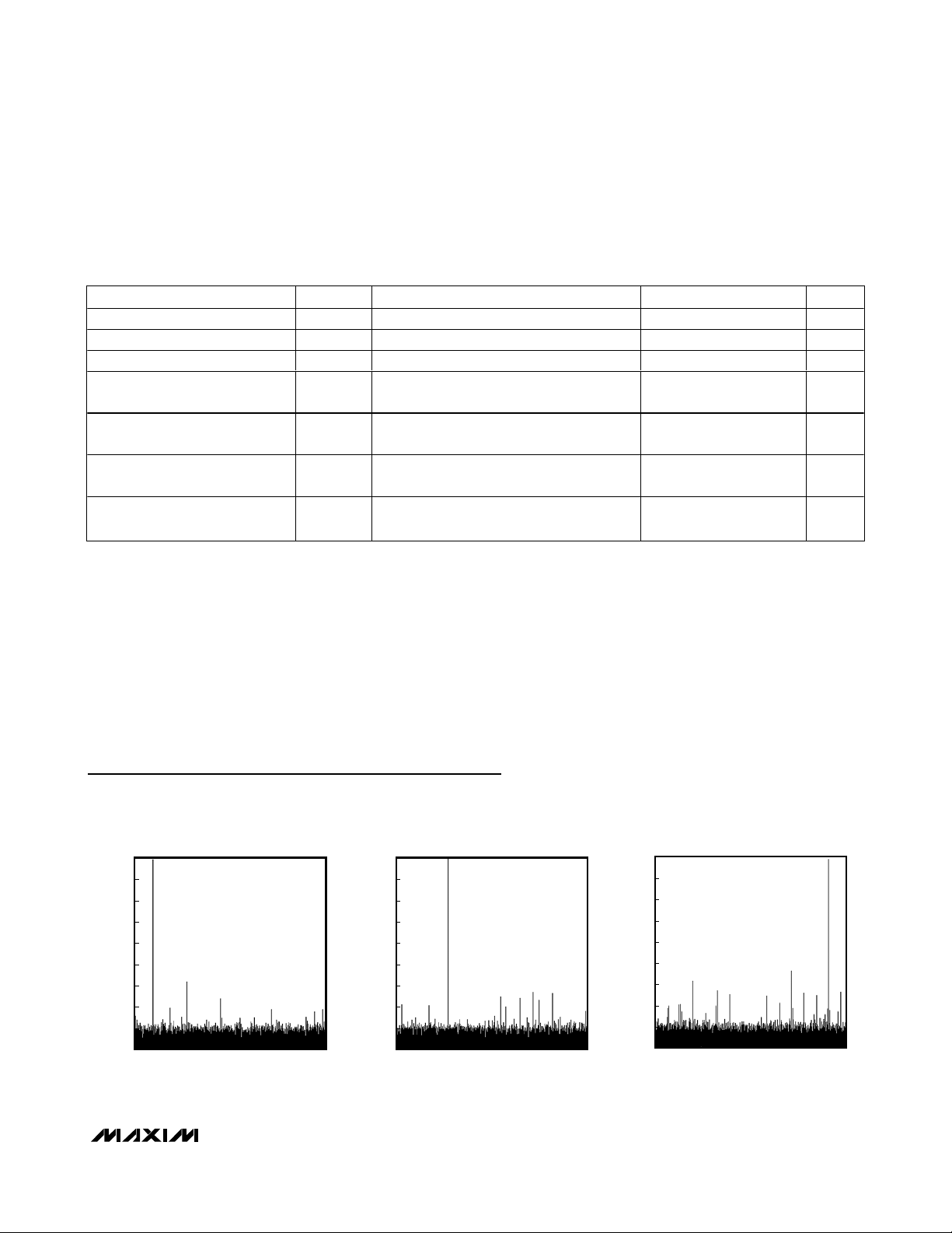
FFT PLOT (16,384-POINT DATA RECORD)
MAX109 toc02
AMPLITUDE (dB)
f
CLK
= 2.21184GHz
f
IN
= 300.105MHz
A
IN
= -1.034dBFS
SNR = 45.1dB
SINAD = 44.8dB
THD = -56.2dBc
SFDR = 62.4dBc
HD2 = -64.4dBc
HD3 = -62.7dBc
0 552.96276.48 829.44 1105.92
414.72138.24 691.20 967.68
ANALOG INPUT FREQUENCY (MHz)
-90
-70
-80
-40
-50
-60
-10
-20
-30
0
0 552.96276.48 829.44 1105.92
414.72138.24 691.20 967.68
FFT PLOT (16,384-POINT DATA RECORD)
MAX109 toc01
ANALOG INPUT FREQUENCY (MHz)
AMPLITUDE (dB)
f
CLK
= 2.21184GHz
f
IN
= 98.145MHz
A
IN
= -0.975dBFS
SNR = 45.2dB
SINAD = 44.8dB
THD = -55.7dBc
SFDR = 57.2dBc
HD2 = -69.6dBc
HD3 = -57.2dBc
-90
-70
-80
-40
-50
-60
-10
-20
-30
0
FFT PLOT (16,384-POINT DATA RECORD)
MAX109 toc03
AMPLITUDE (dB)
f
CLK
= 2.21184GHz
f
IN
= 999.135MHz
A
IN
= -1.059dBFS
SNR = 44.5dB
SINAD = 43.3dB
THD = -49.5dBc
SFDR = 52.1dBc
HD2 = -57.3dBc
HD3 = -52.1dBc
0 552.96276.48 829.44 1105.92
414.72138.24 691.20 967.68
ANALOG INPUT FREQUENCY (MHz)
PARAMETER SYMBOL CONDITIONS MIN TYP MAX UNITS
LVDS Output Rise Time t
LVDS Output Fall Time t
LVDS Differential Skew t
PortD Data Pipeline Delay t
PortC Data Pipeline Delay t
PortB Data Pipeline Delay t
PortA Data Pipeline Delay t
RDATA
FDATA
SKEW1
PDD
PDC
PDB
PDA
20% to 80%, CL < 2pF 500 ps
20% to 80%, CL < 2pF 500 ps
Any two LVDS output signals, except DCO <100 ps
7.5
8.5
9.5
10.5
Clock
Cycles
Clock
Cycles
Clock
Cycles
Clock
Cycles
Page 8
MAX109
8-Bit, 2.2Gsps ADC with Track/Hold Amplifier
and 1:4 Demultiplexed LVDS Outputs
8 _______________________________________________________________________________________
HD2
HD3
(dB
)
Typical Operating Characteristics (continued)
(VCCA = VCCI = VCCD = 5V, VCCO = 3.3V, V
EE
= -5V, GNDA = GNDI = GNDD = GNDO = GNDR = 0V, f
CLK
= 2.21184Gsps, analog
input amplitude at -1dBFS differential, clock input amplitude 10dBm differential, digital output pins differential R
L
= 100Ω. Typical
values are at TJ = +105°C, unless otherwise noted.)
-90
-70
-80
-40
-50
-60
-10
-20
-30
0
FFT PLOT (16,384-POINT DATA RECORD)
MAX109 toc04
AMPLITUDE (dB)
f
CLK
= 2.21184GHz
fIN = 1600.155MHz
A
IN
= -0.992dBFS
SNR = 44.2dB
SINAD = 42.6dB
THD = -47.5dBc
SFDR = 51.1dBc
HD2 = -51.1dBc
HD3 = -52.1dBc
0 552.96276.48 829.44 1105.92
414.72138.24 691.20 967.68
ANALOG INPUT FREQUENCY (MHz)
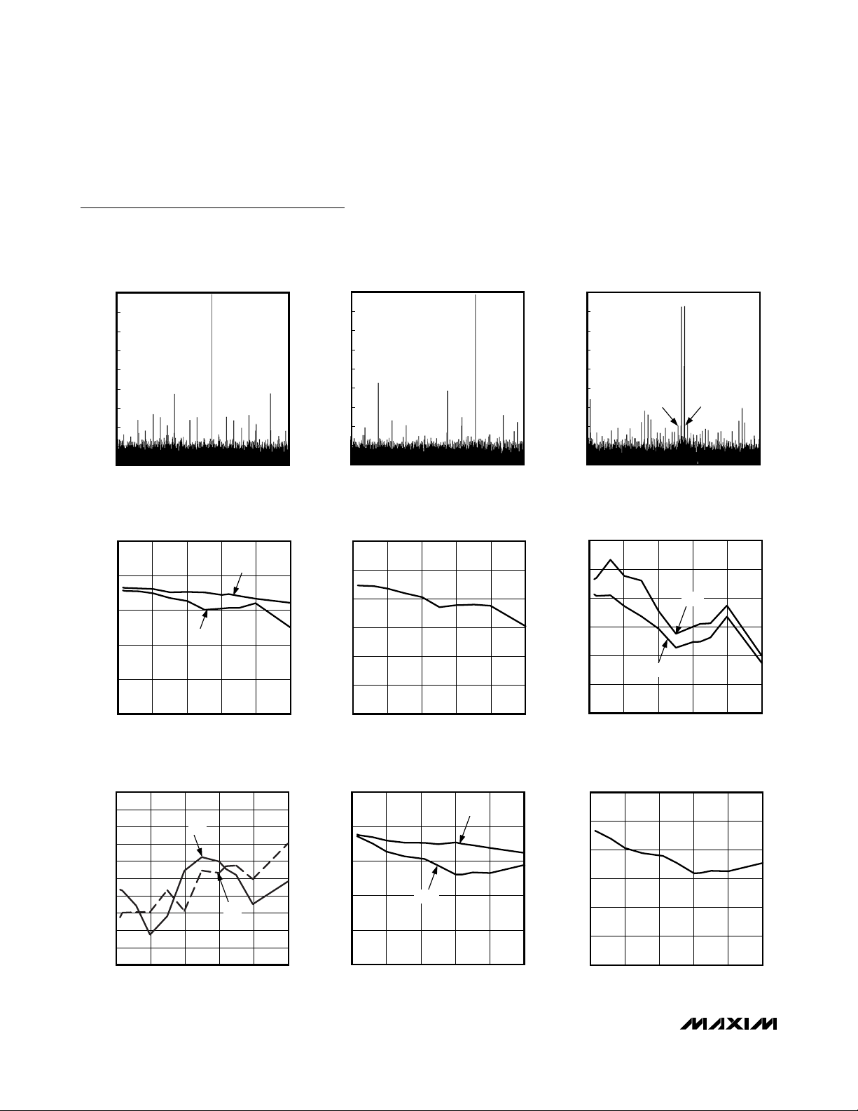
SNR, SINAD vs. ANALOG INPUT FREQUENCY
= 2.21184Gsps, AIN = -1dBFS)
(f
CLK
50
FFT PLOT (16,384-POINT DATA RECORD)
0
-10
-20
-30
-40
-50
AMPLITUDE (dB)
-60
-70
-80
-90
f
= 2.49856GHz
CLK
= 1599.268MHz
f
IN
AIN = -1.059dBFS
SNR = 44.1dB
SINAD = 41.2dB
THD = -44.4dBc
SFDR = 46.1dBc
HD2 = -50.1dBc
HD3 = -46.1dBc
0 624.64312.32 936.96 1249.28
468.48156.16 780.8 1098.12
ANALOG INPUT FREQUENCY (MHz)
MAX109 toc05
AMPLITUDE (dB)
ENOB vs. ANALOG INPUT FREQUENCY
= 2.21184Gsps, AIN = -1dBFS)
(f
CLK
8.0
TTIMD PLOT (16,384-POINT DATA RECORD)
0
f
= 2.21184GHz
CLK
-10
= 1590.165MHz
f
IN1
= 1610.415MHz
f
IN2
-20
-30
-40
-50
-60
-70
-80
-90
= A
A
IN1
IN2
IM3 = -60.8dBc
0 552.96276.48 829.44 1105.92
ANALOG INPUT FREQUENCY (MHz)
-THD, SFDR vs. ANALOG INPUT FREQUENCY
= 2.21184Gsps, AIN = -1dBFS)
(f
CLK
65
= -7.13dBFS
2f
2f
- f
IN2
IN1
414.72138.24 691.20 967.68
- f
IN1
IN2
MAX109 toc06
46
42
38
SNR, SINAD (dB)
34
30
0 500 1000 1500 2000 2500
HD2, HD3 vs. ANALOG INPUT FREQUENCY
= 2.21184Gsps, AIN = -1dBFS)
(f
CLK
-30
-35
-40
-45
c
-50
-55
,
-60
-65
-70
-75
-80
0 500 1000 1500 2000 2500
SINAD
fIN (MHz)
HD3
fIN (MHz)
HD2
SNR
MAX109 toc07
MAX109 toc10
7.5
7.0
6.5
ENOB (Bits)
6.0
5.5
5.0
0 500 1000 1500 2000 2500
fIN (MHz)
SNR, SINAD vs. ANALOG INPUT FREQUENCY
= 2.49856Gsps, AIN = -1dBFS)
(f
CLK
50
SNR
46
42
38
SNR, SINAD (dB)
34
30
0 500 1000 1500 2000 2500
SINAD
fIN (MHz)
MAX109 toc08
MAX109 toc11
60
55
50
-THD, SFDR (dBc)
45
40
35
0 500 1000 1500 2000 2500
SFDR
-THD
fIN (MHz)
ENOB vs. ANALOG INPUT FREQUENCY
= 2.49856Gsps, AIN = -1dBFS)
(f
CLK
8.0
7.5
7.0
6.5
ENOB (Bits)
6.0
5.5
5.0
0 500 1000 1500 2000 2500
fIN (MHz)
MAX109 toc09
MAX109 toc12
Page 9
MAX109
Typical Operating Characteristics (continued)
(VCCA = VCCI = VCCD = 5V, VCCO = 3.3V, V
EE
= -5V, GNDA = GNDI = GNDD = GNDO = GNDR = 0V, f
CLK
= 2.21184Gsps, analog
input amplitude at -1dBFS differential, clock input amplitude 10dBm differential, digital output pins differential R
L
= 100Ω. Typical
values are at TJ = +105°C, unless otherwise noted.)
8-Bit, 2.2Gsps ADC with Track/Hold Amplifier
and 1:4 Demultiplexed LVDS Outputs
_______________________________________________________________________________________
9
-THD, SFDR vs. ANALOG INPUT FREQUENCY
= 2.49856Gsps, AIN = -1dBFS)
(f
CLK
65
60
55
50
-THD, SFDR (dBc)
45
40
35
0 500 1000 1500 2000 2500
SFDR
-THD
fIN (MHz)
ENOB vs. ANALOG INPUT AMPLITUDE
= 2.21184Gsps, fIN = 1600.1550MHz)
(f
CLK
8.0
7.5
7.0
6.5
ENOB (Bits)
6.0
5.5
5.0
-45 -40 -35 -30 -25 -20 -15 -10 -5 0
AIN (dBFS)
HD2, HD3 vs. ANALOG INPUT FREQUENCY
= 2.49865Gsps, AIN = -1dBFS)
(f
CLK
-30
MAX109 toc13
-35
-40
-45
-50
-55
-60
HD2, HD3 (dBc)
-65
-70
-75
-80
0 500 1000 1500 2000 2500
HD3
HD2
fIN (MHz)
MAX109 toc14
SNR, SINAD (dB)
-THD, SFDR vs. ANALOG INPUT AMPLITUDE
= 2.21184Gsps, fIN = 1600.1550MHz)
(f
CLK
60
MAX109 to16
55
50
45
40
35
-THD, SFDR (dBc)
30
25
20
-45 -40 -35 -30 -25 -20 -15 -10 -5 0
SFDR
-THD
AIN (dBFS)
MAX109 toc17
HD2, HD3 (dBc)
SNR, SINAD vs. ANALOG INPUT AMPLITUDE
= 2.21184Gsps, fIN = 1600.1550MHz)
(f
CLK
45
40
35
30
25
20
15
10
5
0
-45 -40 -35 -30 -25 -20 -15 -10 -5 0
HD2, HD3 vs. ANALOG INPUT AMPLITUDE
= 2.21184Gsps, fIN = 1600.1550MHz)
(f
CLK
-20
-25
-30
-35
-40
-45
-50
-55
-60
-65
-70
-45 -40 -35 -30 -25 -20 -15 -10 -5 0
AIN (dBFS)
HD3
HD2
AIN (dBFS)
SNR
MAX109 toc15
SINAD
MAX109 toc18
SNR, SINAD vs. CLOCK SPEED
= 1600MHz, AIN = -1dBFS)
(f
50
46
42
38
SNR, SINAD (dB)
34
30
IN
SNR
SINAD
500 750 1000 1250 1500 1750 2000 2250 2500
f
(MHz)
CLK
MAX109 toc19
ENOB vs. CLOCK SPEED
= 1600MHz, AIN = -1dBFS)
(f
8.0
7.5
7.0
6.5
ENOB (Bits)
6.0
5.5
5.0
IN
500 750 1000 1250 1500 1750 2000 2250 2500
f
(MHz)
CLK
MAX109 toc20
-THD, SFDR vs. CLOCK SPEED
= 1600MHz, AIN = -1dBFS)
(f
60
55
50
45
-THD, SFDR (dBc)
40
35
IN
SFDR
-THD
500 750 1000 1250 1500 1750 2000 2250 2500
f
(MHz)
CLK
MAX109 toc21
Page 10

MAX109
8-Bit, 2.2Gsps ADC with Track/Hold Amplifier
and 1:4 Demultiplexed LVDS Outputs
10 ______________________________________________________________________________________
Typical Operating Characteristics (continued)
(VCCA = VCCI = VCCD = 5V, VCCO = 3.3V, V
EE
= -5V, GNDA = GNDI = GNDD = GNDO = GNDR = 0V, f
CLK
= 2.21184Gsps, analog
input amplitude at -1dBFS differential, clock input amplitude 10dBm differential, digital output pins differential R
L
= 100Ω. Typical
values are at TJ = +105°C, unless otherwise noted.)
HD2, HD3 vs. CLOCK SPEED
(f
IN
= 1600MHz, AIN = -1dBFS)
f
CLK
(MHz)
HD2, HD3 (dBc)
MAX109 toc22
500 750 1000 1250 1500 1750 2000 2250 2500
-75
-70
-65
-60
-55
-50
-45
-40
HD3
HD2
SNR, SINAD (dB)
-THD, SFDR (dBc)
SNR, SINAD vs. VCCD
= 1600.1550MHz, AIN = -1dBFS)
(f
IN
50
VCCA = VCCI = 5V
O = 3.3V
V
CC
48
= -5V
V
EE
46
44
42
40
38
36
4.75 4.85 4.95 5.05 5.15 5.25
SNR
SINAD
VCCD (V)
-THD, SFDR vs. V
EE
(fIN = 1600.1550MHz, AIN = -1dBFS)
53
VCCA = VCCI = 5V
52
D = 5V
V
CC
O = 3.3V
V
CC
51
50
49
48
47
46
45
44
-5.25 -5.15 -5.05 -4.95 -4.85 -4.75
SFDR
-THD
VEE (V)
SNR, SINAD vs. VCCA/VCCI
= 1600.1550MHz, AIN = -1dBFS)
(f
IN
50
VCCA AND VCCI CONNECTED
TOGETHER
48
46
44
42
SNR, SINAD (dB)
40
VCCD = 5V
38
O = 3.3V
V
CC
= -5V
V
EE
36
4.75 4.85 4.95 5.05 5.15 5.25
SNR
SINAD
VCCA/VCCI (V)
MAX109 toc23
-THD, SFDR (dBc)
-THD, SFDR vs. VCCD
= 1600.1550MHz, AIN = -1dBFS)
(f
IN
53
MAX109 toc25
52
51
50
49
48
-THD, SFDR (dBc)
47
46
VCCA = VCCI = 5V
O = 3.3V
V
CC
45
= -5V
V
EE
44
4.75 4.85 4.95 5.05 5.15 5.25
SFDR
VCCD (V)
-THD
MAX109 toc26
SNR, SINAD (dB)
INTEGRAL NONLINEARITY
vs. DIGITAL OUTPUT CODE
(262,144-POINT DATA RECORD)
MAX109 toc28
1.0
0.8
0.6
0.4
0.2
0
INL (LSB)
-0.2
-0.4
-0.6
-0.8
-1.0
0 96 12832 64 160 192 224 256
DIGITAL OUTPUT CODE
MAX109 toc29
1.0
0.8
0.6
0.4
0.2
DNL (LSB)
-0.2
-0.4
-0.6
-0.8
-1.0
53
52
51
50
49
48
47
46
45
44
4.75 4.85 4.95 5.05 5.15 5.25
50
48
46
44
42
40
38
36
-5.25 -5.15 -5.05 -4.95 -4.85 -4.75
0
0 96 12832 64 160 192 224 256
-THD, SFDR vs. VCCA/VCCI
= 1600.1550MHz, AIN = -1dBFS)
(f
IN
V
AND VCCI CONNECTED
CCA
TOGETHER
SFDR
VCCD = 5V
O = 3.3V
V
CC
= -5V
V
EE
VCCA/VCCI (V)
SNR, SINAD vs. V
(fIN = 1600.1550MHz, AIN = -1dBFS)
VCCA = VCCI = 5V
D = 5V
V
CC
O = 3.3V
V
CC
SNR
SINAD
VEE (V)
DIFFERENTIAL NONLINEARITY
vs. DIGITAL OUTPUT CODE
(262,144-POINT DATA RECORD)
DIGITAL OUTPUT CODE
MAX109 toc24
-THD
EE
MAX109 toc27
MAX109 toc30
Page 11

MAX109
8-Bit, 2.2Gsps ADC with Track/Hold Amplifier
and 1:4 Demultiplexed LVDS Outputs
______________________________________________________________________________________
11
Typical Operating Characteristics (continued)
(VCCA = VCCI = VCCD = 5V, VCCO = 3.3V, V
EE
= -5V, GNDA = GNDI = GNDD = GNDO = GNDR = 0V, f
CLK
= 2.21184Gsps, analog
input amplitude at -1dBFS differential, clock input amplitude 10dBm differential, digital output pins differential R
L
= 100Ω. Typical
values are at TJ = +105°C, unless otherwise noted.)
GAIN (dB)
FULL-POWER INPUT BANDWIDTH
vs. ANALOG INPUT FREQUENCY (A
1
0
-1
-2
-3
-4
-5
-6
10 100 1000 10,000
ANALOG INPUT FREQUENCY (MHz)
= -1dBFS)
IN
ANALOG/DIGITAL POWER DISSIPATION
A/VCCI/VCCD/-V
vs. V
CC
EE
(fIN = 1600.1550MHz, AIN = -1dBFS)
6800
VCCO = 3.3V
A = VCCI = VCCD = 4.75V to 5V
V
CC
= -4.75V to -5.25V
V
6500
EE
6200
SMALL-SIGNAL INPUT BANDWIDTH
vs. ANALOG INPUT FREQUENCY
= -20dBFS)
(A
IN
MAX109 toc32
ANALOG INPUT FREQUENCY (MHz)
MAX109 toc31
1
0
-1
-2
-3
GAIN (dB)
-4
-5
-6
10 100 1000 10,000
OUTPUT DRIVER POWER DISSIPATION
O (fIN = 1600.1550MHz, AIN = -1dBFS)
vs. V
CC
900
VCCO = 3V to 3.6V
A = VCCI = VCCD = 5V
V
850
800
CC
= -5V
V
EE
MAX109 toc35
MAX109 toc34
REFERENCE VOLTAGE vs. VCCA/VCCI
2.4995
VCCA AND VCCI
CONNECTED TOGETHER
2.4985
2.4975
2.4965
(V)
REFOUT
2.4955
V
2.4945
2.4935
2.4925
O = 3.3V
V
CC
D = 5V
V
CC
= -5V
V
EE
4.75 4.85 4.95 5.05 5.15 5.25
SNR, SINAD vs. TEMPERATURE
= 1600.1550MHz, AIN = -1dBFS)
(f
IN
45
43
41
VCCA/VCCI (V)
SINAD
SNR
MAX109 toc33
MAX109 toc36
5900
POWER DISSIPATION (mW)
5600
5300
4.75 4.85 4.95 5.05 5.15 5.25
VCCA/VCCI/VCCD/-V
(V)
EE
ENOB vs. TEMPERATURE
= 1600.1550MHz, AIN = -1dBFS)
(f
IN
7.50
7.25
7.00
6.75
6.50
ENOB (Bits)
6.25
6.00
5.75
5.50
-40 -15 10 35 60 85
[-22.1] [7.5] [37.1] [66.7] [96.3] [125.9]
TEMPERATURE (°C)
[DIE TEMPERATURE (°C)]
750
POWER DISSIPATION (mW)
700
650
3.0 3.1 3.2 3.3 3.4 3.5 3.6
54
52
MAX109 toc37
50
48
46
44
-THD, SFDR (dBc)
42
40
38
-40 -15 10 35 60 85
[-22.1] [7.5] [37.1] [66.7] [96.3] [125.9]
VCCO (V)
-THD, SFDR vs. TEMPERATURE
= 1600.1550MHz, AIN = -1dBFS)
(f
IN
SFDR
-THD
TEMPERATURE (°C)
[DIE TEMPERATURE (°C)]
MAX109 toc38
39
SNR, SINAD (dB)
37
35
-40 -15 10 35 60 85
[-22.1] [7.5] [37.1] [66.7] [96.3] [125.9]
TEMPERATURE (°C)
[DIE TEMPERATURE (°C)]
HD2, HD3 vs. TEMPERATURE
= 1600.1550MHz, AIN = -1dBFS)
(f
IN
-44
-46
-48
-50
HD2, HD3 (dBc)
-52
-54
-56
-40 -15 10 35 60 85
[-22.1] [7.5] [37.1] [66.7] [96.3] [125.9]
HD3
TEMPERATURE (°C)
[DIE TEMPERATURE (°C)]
HD2
MAX109 toc39
Page 12

MAX109
8-Bit, 2.2Gsps ADC with Track/Hold Amplifier
and 1:4 Demultiplexed LVDS Outputs
12 ______________________________________________________________________________________
12 ______________________________________________________________________________________
Pin Description
PIN NAME FUNCTION
A1, A2, B1, B2,
C1–C5, D5,
L1–L4, U5, V1–V4,
W1, W2, Y1, Y2
A3, A4, B3, B4,
D1–D4, K1–K4,
U1–U4, W3, W4,
Y3, Y4
A9, B9, C10, D10,
U10, V10, W10,
Y10
A10, B10, C11,
D11, U11, V11,
W11, Y11
A11, A19, B11,
B18, C12, C18,
D12, D18, E17,
U17, V17, W17,
Y17, U12, V12,
W12, Y12
A12, A18, B12,
B13, B17, C13,
C17, D13, D17,
U13, U16, V13,
V16, W13, W16,
Y13, Y16
H17–H20,
P17–P20, U15,
V15, W15, Y15
V
O LVDS Output Power Supply. Accepts an input-voltage range of 3.3V ±10%.
CC
GNDO LVDS Output Ground. Ground connection for LVDS output drivers.
V
D Digital Logic Power Supply. Accepts an input-voltage range of 5V ±5%.
CC
GNDD Digital Ground. Ground connection for digital logic circuitry.
V
A Analog Supply Voltage for Comparator Array. Accepts an input-voltage range of 5V ±5%.
CC
GNDA Analog Ground. Ground connection for comparator array.
V
CC
Analog Supply Voltage. Analog power supply (positive rail) for T/H amplifier. Accepts an input-
I
voltage range of 5V ±5%.
E18, F17–F20,
J17, J18, J19,
N17, N18, N19,
T17–T20, U18
D 19, D 20, E 19,
E 20, G17–G20,
J20, K17, K18,
K19, L17–L20,
M 17, M 18, M 19,
N 20, R17–R20,
U 14, U 19, U 20,
V 14, V 19, V 20,
W14, Y 14
V
EE
GNDI Analog Ground. Ground connection for the T/H amplifier.
Negative Power Supply. Analog power supply (negative rail) for the T/H amplifier. Accepts an
input-voltage range of -5V ±5%.
PIN NAME
Page 13

MAX109
8-Bit, 2.2Gsps ADC with Track/Hold Amplifier
and 1:4 Demultiplexed LVDS Outputs
______________________________________________________________________________________ 13
______________________________________________________________________________________ 13
Pin Description (continued)
PIN NAME FUNCTION
A14 CLKP True/Positive Sampling Clock Input. Positive terminal for differential input configuration.
A16 CLKN
A13, A15, A17,
B14, B15, B16,
C14, C15, C16,
D14, D15, D16
B20 SAMPADJ
B19 DELGATE1
C19 DELGATE0
Y20 REFIN
Y19 REFOUT Internal Reference Output. Connect to REFIN, if using the internal 2.5V bandgap reference.
V18, W18, Y18 GNDR
M20 INP
K20 INN
W20 VOSADJ
M4 DORP
M3 DORN
M2 DCOP
M1 DCON
CLKCOM 50Ω Clock Termination Return
Complementary/Negative Sampling Clock Input. Negative terminal for differential input
configuration.
Sampling Point Adjustment Input. Allows the user to adjust the sampling event by applying a
voltage between 0 to 2.5V to this input.
Timing Delay Adjustment. Coarse (MSB) adjustment for the timing between T/H amplifier and
quantizer.
Timing Delay Adjustment. Coarse (LSB) adjustment for the timing between T/H amplifier and
quantizer.
Reference Voltage Input. For applications requiring improved gain performance and referencevoltage adjustability, allows the user to utilize the REFIN input by applying a more accurate and
adjustable reference source. This input accepts an input-voltage range of 2.5V ±10%.
Bandgap Reference Ground. Ground connection for the internal bandgap reference and its
related circuitry.
True/Positive Analog Input Terminal. For single-ended signals, apply signal to INP and reverseterminate INN to GNDI with a 50Ω resistor.
C om p l em entar y/N eg ati ve Anal og Inp ut Ter m i nal . For si ng l ed - end ed si g nal s, r ever se- ter m i nate IN N to
GN D I w i th a 50Ω r esi stor and ap p l y the si g nal d i r ectl y to IN P .
Analog Voltage Input to Adjust the Converter Offset. This input accepts an input-voltage range of
0 to 2.5V allowing the offset to be adjusted at roughly ±10 LSB.
True/Positive LVDS Data-Overrange Output Bit. This output flags over- and under-range
conditions of the data converter.
Complementary/Negative LVDS Data-Overrange Output Bit. This output flags over- and underrange conditions on the data converter.
True/Positive LVDS Data Clock Output. Synchronize user-supplied data-capture board or dataacquisition system to this clock.
Complementary/Negative LVDS Data Clock Output. Synchronize user-supplied data-capture
board or data-acquisition system to this clock.
PIN NAME
Page 14

MAX109
8-Bit, 2.2Gsps ADC with Track/Hold Amplifier
and 1:4 Demultiplexed LVDS Outputs
14 ______________________________________________________________________________________
Pin Description (continued)
PIN NAME FUNCTION
Y5 QDR
W5 DDR
V5 PRN
D9 RSTINP True/Positive Reset Input
C9 RSTINN Complementary/Negative Reset Input
B5 RSTOUTP True/Positive LVDS Reset Output
A5 RSTOUTN Complementary LVDS Reset Output
B8 D7P True/Positive Output Bit D7P, PortD, Bit 7
A8 D7N Complementary/Negative Output Bit D7N, PortD, Bit 7
B6 D6P True/Positive Output Bit D6P, PortD, Bit 6
A6 D6N Complementary/Negative Output Bit D6N, PortD, Bit 6
F2 D5P True/Positive Output Bit D5P, PortD, Bit 5
F1 D5N Complementary/Negative Output Bit D5N, PortD, Bit 5
H2 D4P True/Positive Output Bit D4P, PortD, Bit 4
H1 D4N Complementary/Negative Output Bit D4N, PortD, Bit 4
N2 D3P True/Positive Output Bit D3P, PortD, Bit 3
N1 D3N Complementary/Negative Output Bit D3N, PortD, Bit 3
R2 D2P True/Positive Output Bit D2P, PortD, Bit 2
R1 D2N Complementary/Negative Output Bit D2N, PortD, Bit 2
W6 D1P True/Positive Output Bit D1P, PortD, Bit 1
Y6 D1N Complementary/Negative Output Bit D1N, PortD, Bit 1
W8 D0P True/Positive Output Bit D0P, PortD, Bit 0
Y8 D0N Complementary/Negative Output Bit, D0N, PortD, Bit 0
D8 C7P True/Positive Output Bit C7P, PortC, Bit 7
C8 C7N Complementary/Negative Output Bit C7N, PortC, Bit 7
D6 C6P True/Positive Output Bit C6P, PortC, Bit 6
C6 C6N Complementary/Negative Output Bit C6N, PortC, Bit 6
F4 C5P True/Positive Output Bit C5P, PortC, Bit 5
F3 C5N Complementary/Negative Output Bit C5N, PortC, Bit 5
H4 C4P True/Positive Output Bit C4P, PortC, Bit 4
H3 C4N Complementary/Negative Output Bit C4N, PortC, Bit 4
N4 C3P True/Positive Output Bit C3P, PortC, Bit 3
N3 C3N Complementary/Negative Output Bit C3N, PortC, Bit 3
R4 C2P True/Positive Output Bit C2P, PortC, Bit 2
Quad Data Rate Input (CMOS). Connect to GNDD for the default data rate to be applied.
Connect to V
Double Data Rate Input (CMOS). Connect to GNDD for the standard data rate to be applied.
Connect to V
Pseudorandom Number Generator Enable Input (CMOS). When enabled, pseudorandom
patterns appear on all four LVDS output ports (PortA, PortB, PortC, and PortD).
D to achieve four times the specified data rate.
CC
D to achieve two times the specified data rate.
CC
Page 15

MAX109
8-Bit, 2.2Gsps ADC with Track/Hold Amplifier
and 1:4 Demultiplexed LVDS Outputs
______________________________________________________________________________________ 15
Pin Description (continued)
PIN NAME FUNCTION
R3 C2N Complementary/Negative Output Bit C2N, PortC, Bit 2
U6 C1P True/Positive Output Bit C1P, PortC, Bit 1
V6 C1N Complementary/Negative Output Bit C1N, PortC, Bit 1
U8 C0P True/Positive Output Bit C0P, PortC, Bit 0
V8 C0N Complementary/Negative Output Bit C0N, PortC, Bit 0
B7 B7P True/Positive Output Bit B7P, PortB, Bit 7
A7 B7N Complementary/Negative Output Bit B7N, PortB, Bit 7
E2 B6P True/Positive Output Bit B6P, PortB, Bit, 6
E1 B6N Complementary/Negative Output Bit B6N, PortB, Bit 6
G2 B5P True/Positive Output Bit B5P, PortB, Bit 5
G1 B5N Complementary/Negative Output Bit B5N, PortB, Bit 5
J2 B4P True/Positive Output Bit B4P, PortB, Bit 4
J1 B4N Complementary/Negative Output Bit B4N, PortB, Bit 4
P2 B3P True/Positive Output Bit B3P, PortB, Bit 3
P1 B3N Complementary/Negative Output Bit B3N, PortB, Bit 3
T2 B2P True/Positive Output Bit B2P, PortB, Bit 2
T1 B2N Complementary/Negative Output Bit B2N, PortB, Bit 2
W7 B1P True/Positive Output Bit B1P, PortB, Bit 1
Y7 B1N Complementary/Negative Output Bit B1N, PortB, Bit 1
W9 B0P True/Positive Output Bit B0P, PortB, Bit 0
Y9 B0N Complementary/Negative Output Bit B0N, PortB, Bit 0
D7 A7P True/Positive Output Bit A7P, PortA, Bit 7
C7 A7N Complementary/Negative Output Bit A7N, PortA, Bit 7
E4 A6P True/Positive Output Bit A6P, PortA, Bit 6
E3 A6N Complementary/Negative Output Bit A6N, PortA, Bit 6
G4 A5P True/Positive Output Bit A5P, PortA, Bit 5
G3 A5N Complementary/Negative Output Bit A5N, PortA, Bit 5
J4 A4P True/Positive Output Bit A4P, PortA, Bit 4
J3 A4N Complementary/Negative Output Bit A4N, PortA, Bit 4
P4 A3P True/Positive Output Bit A3P, PortA, Bit 3
P3 A3N Complementary/Negative Output Bit A3N, PortA, Bit 3
T4 A2P True/Positive Output Bit A2P, PortA, Bit 2
T3 A2N Complementary/Negative Output Bit A2N, PortA, Bit 2
Page 16

MAX109
Detailed Description
The MAX109 is an 8-bit, 2.2Gsps flash analog-to-digital
converter (ADC) with an on-chip T/H amplifier and 1:4
demultiplexed high-speed LVDS outputs. The ADC
(Figure 1) employs a fully differential 8-bit quantizer and
a unique encoding scheme to limit metastable states
and ensures no error exceeds a maximum of 1 LSB.
An integrated 1:4 output demultiplexer simplifies interfacing to the part by reducing the output data rate to
one-quarter the sampling clock rate. This demultiplexer
circuit has integrated reset capabilities that allow multiple MAX109 converters to be time-interleaved to
achieve higher effective sampling rates.
When clocked at 2.2Gsps, the MAX109 provides a typical
effective number of bits (ENOB) of 6.9 bits at an analog
input frequency of 1600MHz. The MAX109 analog input is
designed for both differential and single-ended use with a
500mV
P-P
full-scale input range. In addition, this fast ADC
features an on-chip 2.5V precision bandgap reference. In
order to improve the MAX109 gain error further, an external reference may be used (see the
Internal Reference
section).
Principle of Operation
The architecture of the MAX109 provides the fastest
multibit conversion of all common integrated ADC
designs. The key to its architecture is an innovative,
high-performance comparator design. The MAX109
quantizer and its encoding logic translate the comparator outputs into a parallel 8-bit output code and pass
the binary code on to the 1:4 demultiplexer. Four separate ports (PortA, PortB, PortC, and PortD) output true
LVDS data at speeds of up to 550Msps per port
(depending on how the demultiplexer section is set on
the MAX109).
The ideal transfer function appears in Figure 2.
On-Chip Track/Hold Amplifier
As with all ADCs, if the input waveform is changing
rapidly during conversion, ENOB and signal-to-noise
ratio (SNR) specifications will degrade. The MAX109’s
on-chip, wide-bandwidth (2.8GHz) T/H amplifier
reduces this effect and increases the ENOB performance significantly, allowing precise capture of fastchanging analog data at high conversion rates.
The T/H amplifier accepts and buffers both DC- and
AC-coupled analog input signals and allows a full-scale
signal input range of 500mV
P-P
. The T/H amplifier’s dif-
ferential 50Ω input termination simplifies interfacing to
the MAX109 with controlled impedance lines. Figure 3
shows a simplified diagram of the T/H amplifier stage
internal to the MAX109.
8-Bit, 2.2Gsps ADC with Track/Hold Amplifier
and 1:4 Demultiplexed LVDS Outputs
16 ______________________________________________________________________________________
Pin Description (continued)
Figure 2. Ideal Transfer Function
PIN NAME FUNCTION
U7 A1P True/Positive Output Bit A1P, PortA, Bit 1
V7 A1N Complementary/Negative Output Bit A1N, PortA, Bit 1
U9 A0P True/Positive Output Bit A0P, PortA, Bit 0
V9 A0N Complementary/Negative Output Bit A0N, PortA, Bit 0
W19 TEMPMON Temp er atur e M oni tor Outp ut. Resul ting outp ut vol tage cor r esp onds to d i e temp er atur e.
A20, C20 T.P. Test Point. Do not connect.
OVERRANGE +
OVERRANGE
255
255
254
129
128
127
126
DIGITAL OUTPUT
3
2
1
0
0
ANALOG INPUT
(-FS + 1 LSB)
+FS
(+FS - 1 LSB)
Page 17

MAX109
8-Bit, 2.2Gsps ADC with Track/Hold Amplifier
and 1:4 Demultiplexed LVDS Outputs
______________________________________________________________________________________ 17
Aperture width, delay, and jitter are parameters that
affect the dynamic performance of high-speed converters. Aperture jitter, in particular, directly influences SNR
and limits the maximum slew rate (dV/dt) that can be
digitized without contributing significant errors. The
MAX109’s innovative T/H amplifier design limits aperture jitter typically to 0.2ps.
Aperture Width, Aperture Jitter, and Aperture Delay
Aperture width (tAW) is the time the T/H circuit requires
to disconnect the hold capacitor from the input circuit
(e.g., to turn off the sampling bridge and put the T/H
unit in hold mode). Aperture jitter (t
AJ
) is the sample-tosample variation in the time between the samples.
Aperture delay (t
AD
) is the time defined between the
rising edge of the sampling clock and the instant when
an actual sample event is occurring (Figure 4).
Clock System
The MAX109 clock signals are terminated with 50Ω to
the CLKCOM pin. The clock system provides clock signals, T/H amplifier, quantizer, and all back-end digital
blocks. The MAX109 also produces a digitized output
clock for synchronization with external FPGA or datacapture devices. Note that there is a 1.6ns delay
between the clock input (CLKP/CLKN) and its digitized
output representation (DCOP/DCON).
Sampling Point Adjustment (SAMPADJ)
The proper sampling point can be adjusted by utilizing
SAMPADJ as the control line. SAMPADJ accepts an
input-voltage range of 0 to 2.5V, correlating with up to
32ps timing adjustment. The nominal open-circuit voltage corresponds to the minimum sampling delay. With
an input resistance R
SAMPADJ
of typically 50kΩ, this
pin can be adjusted externally with a 10kΩ potentiometer connected between REFOUT and GNDI to adjust for
the proper sampling point.
T/H Amplifier to Quantizer Capture Point
Adjustment (DELGATE0, DELGATE1)
Another important feature of the MAX109, is the selection of the proper quantizer capture point between the
T/H amplifier and the ADC core. Depending on the
selected sampling speed for the application, two control lines can be utilized to set the proper capture point
between these two circuits. DELGATE0 (LSB) and DELGATE1 (MSB) set the
coarse
timing of the proper capture point. Using these control lines allow the user to
adjust the time after which the quantizer latches
held
data from the T/H amplifier between 25ps and 50ps
(Table 1). This timing feature enables the MAX109 T/H
amplifier to settle its output properly before the quantizer captures and digitizes the data, thereby achieving
the best dynamic performance for any application.
Figure 3. Internal Structure of the 3.2GHz T/H Amplifier
Figure 4. T/H Aperture Timing
SIMPLIFIED DIAGRAM
(INPUT ESD PROTECTION
NOT SHOWN).
INP
INN
GNDI
CLKP
CLKN
CLKCOM
CLKN
CLKP
ANALOG
INPUT
SAMPLED
DATA (T/H)
T/H
INPUT
AMPLIFIER
T/H
50Ω50Ω
CLOCK
SPLITTER
50Ω50Ω
t
AW
t
AD
TRACK TRACK
t
AJ
HOLD
APERTURE DELAY (t
APERTURE WIDTH (t
APERTURE JITTER (t
AMPLIFIER
C
GNDI
AD
AW
AJ
BUFFER
TO
COMPARATORS
HOLD
TO
COMPARATORS
)
)
)
Page 18

MAX109
Internal Reference
The MAX109 features an on-chip 2.5V precision
bandgap reference used to generate the full-scale
range for the data converter. Connecting REFIN with
REFOUT applies the reference output to the positive
input of the reference buffer. The buffer’s negative input
is internally connected to GNDR. It is recommended
that GNDR be connected to GNDI on the user’s application board.
If required, REFOUT can source up to 2.5mA to supply
other external devices. Additionally, an adjustable
external reference can be used to adjust the ADC’s fullscale range. To use an external reference supply, connect a high-precision bandgap reference to the REFIN
pin and leave the REFOUT pin floating. REFIN has a
typical input resistance R
REFIN
of 5kΩ and accepts
input voltages of 2.5V ±10%.
Digital LVDS Outputs
The MAX109 provides data in offset binary format to
differential LVDS outputs on four output ports (PortA,
PortB, PortC, and PortD). A simplified circuit schematic
of the LVDS output cells is shown in Figure 5. All LVDS
outputs are powered from the output driver supply
VCCO, which can be operated at 3.3V ±10%. The
MAX109 LVDS outputs provide a differential outputvoltage swing of 600mV
P-P
with a common-mode voltage of approximately 1.2V, and must be differentially
terminated at the far end of each transmission line pair
(true and complementary) with 100Ω.
Data Out-of-Range Operation
(DORP, DORN)
A single differential output pair (DORP, DORN) is provided to flag an out-of-range condition, if the applied
signal is outside the allowable input range, where outof-range is above positive full scale (+FS) or below
negative full scale (-FS). The DORP/DORN transitions
high/low whenever any of the four output ports (PortA,
PortB, PortC, and PortD) display out-of-range data.
DORP/DORN features the same latency as the ADC
output data and is demultiplexed in a similar fashion, so
that this out-of-range signal and the data samples are
time-aligned.
Demultiplexer Operation
The MAX109’s internal 1:4 demultiplexer spreads the
ADC core’s 8-bit data across 32 true LVDS outputs and
allows for easy data capture in three different modes.
Two TTL/CMOS-compatible inputs are utilized to create
the different modes: SDR (standard data rate), DDR
8-Bit, 2.2Gsps ADC with Track/Hold Amplifier
and 1:4 Demultiplexed LVDS Outputs
18 ______________________________________________________________________________________
Table 1. Timing Adjustments for T/H
Amplifier and Quantizer
Table 2. Data Rate Selection for
Demultiplexer Operation
Figure 5. Simplified LVDS Output Circuitry
X = Do not care.
DELGATE1 DELGATE0
0 1 25ps
1 0 50ps
T IM E DEL A Y
B ET WEEN
T /H A N D
Q U A N T IZ ER
RECOMMENDED
FOR CLOCK
SPEEDS OF
f
= 2.2Gsps
CLK
to 2.5Gsps
f
= 1.75Gsps
CLK
to 2.2Gsps
CMFB
CMFB:
COMMON-MODE
FEEDBACK
DDR QDR DEMULTIPLEXER OPERATION
0X
10
11
SDR mode, PortA, PortB, PortC, and
PortD enabled, 550Msps per port
DDR mode, PortA, PortB, PortC, and
PortD enabled, 550Msps per port
QDR mode, PortA, PortB, PortC, and
PortD enabled, 550Msps per port
O
V
CC
AOP–A7P
BOP–B7P
COP–C7P
DOP–D7P
GNDO
DCOP
RSTOUTP
AON–A7N
BON–B7N
CON–C7N
DON–D7N
DCON
RSTOUTN
DCO
SPEED
f
CLK
f
CLK
f
C LK
/ 4
/ 8
/ 16
O
V
CC
GNDO
Page 19

(double data rate), and QDR (quadruple data rate).
Setting these two bits for different modes allows the
user to update and process the outputs at one-quarter
(SDR mode), one-eighth (DDR mode), or one-sixteenth
(QDR mode) the sampling clock (Table 2), relaxing the
need for an ultra-fast FPGA or data-capture interface.
Data is presented on all four ports of the converterdemultiplexer circuit outputs. Note that there is a data
latency between the sampled data and each of the output ports. The data latency is 10.5 clock cycles for
PortA, 9.5 clock cycles for PortB, 8.5 clock cycles for
PortC, and 7.5 clock cycles for PortD. This holds true for
all demultiplexer modes. Figures 6, 7, and 8 display the
demultiplexer timing for f
CLK
/ 4, f
CLK
/ 8, and f
CLK
/ 16
modes.
Pseudorandom Number (PRN) Generator
The MAX109 features a PRN generator that enables the
user to test the demultiplexed digital outputs at full
clock speed and with a known test pattern. The PRN
generator is a combination of shift register and feedback logic with 255 states. When PRN is high, the inter-
MAX109
8-Bit, 2.2Gsps ADC with Track/Hold Amplifier
and 1:4 Demultiplexed LVDS Outputs
______________________________________________________________________________________ 19
Table 3. Pseudorandom Number
Generator Patterns
Figure 6. Timing Diagram for SDR Mode, f
CLK
/ 4 Mode
ADC SAMPLE NUMBER
CLKN
CLKP
DCON
DCOP
PORTA DATA
PORTB DATA
PORTC DATA
PORTD DATA
N N + 1 N + 2 N + 3 N + 4 N + 5
NOTE: THE LATENCY TO THE D PORT IS 7.5 CLOCK CYCLES, THE LATENCY TO THE C PORT IS 8.5 CLOCK CYCLES, THE LATENCY TO THE B
PORT IS 9. 5 CLOCK CYCLES, AND THE LATENCY TO THE A PORT IS 10.5 CLOCK CYCLES. ALL DATA POR TS (PORTA, PORTB, PORT C, AND
PORTD) ARE UPDATED ON THE RISING EDGE OF THE DCOP CLOCK.
ADC SAMPLES ON THE RISING EDGE OF CLKP
N + 6 N + 7 N + 8 N + 9 N + 10 N + 11 N + 12 N + 13 N + 14 N + 15 N + 16 N + 17 N + 18 N + 19
t
t
PD1
PWH
t
PWL
t
SAMPLE HERE
CLK
N + 1
N + 2
N + 3
N + 4N
t
PD2
CODE OUTPUT PRN PATTERN
1 0 0 0 0 0 0 0 1
2 0 0 0 0 0 0 1 0
3 0 0 0 0 0 1 0 0
4 0 0 0 0 1 0 0 0
5 0 0 0 1 0 0 0 1
6 0 0 1 0 0 0 1 1
7 0 1 0 0 0 1 1 1
8 1 0 0 0 1 1 1 0
9 0 0 0 1 1 1 0 0
10 0 0 1 1 1 0 0 0
——
——
250 0 0 1 1 0 1 0 0
251 0 1 1 0 1 0 0 0
252 1 1 0 1 0 0 0 0
253 1 0 1 0 0 0 0 0
254 0 1 0 0 0 0 0 0
255 1 0 0 0 0 0 0 0
N + 5
N + 6
N + 7
N + 8
Page 20

MAX109
8-Bit, 2.2Gsps ADC with Track/Hold Amplifier
and 1:4 Demultiplexed LVDS Outputs
20 ______________________________________________________________________________________
Figure 7. Timing Diagram for DDR Mode, f
CLK
/ 8 Mode
Figure 8. Timing Diagram for QDR Mode, f
CLK
/ 16 Mode
ADC SAMPLE NUMBER
CLKN
CLKP
DCON
N N + 1 N + 2 N + 3 N + 4 N + 5
DCOP
PORTA DATA
PORTB DATA
PORTC DATA
PORTD DATA
NOTE: THE LATENCY TO THE D PORT IS 7.5 CLOCK CYCLES, THE LATENCY TO THE C PORT IS 8.5 CLOCK CYCLES, THE LATENCY TO THE B
PORT IS 9. 5 CLOCK CYCLES, AND THE LATENCY TO THE A PORT IS 10.5 CLOCK CYCLES. ALL DATA POR TS (PORTA, PORTB, PORT C, AND
PORTD) ARE UPDATED ON THE RISING EDGE OF THE DCOP CLOCK.
ADC SAMPLE NUMBER
ADC SAMPLES ON THE RISING EDGE OF CLKP
N + 6 N + 7 N + 8 N + 9 N + 10 N + 11 N + 12 N + 13 N + 14 N + 15 N + 16 N + 17 N + 18 N + 19
SAMPLE HERE
N + 1
N + 2
N + 3
N + 4N
ADC SAMPLES ON THE RISING EDGE OF CLKP
N + 5
N + 6
N + 7
N + 8
t
PD1DDR
t
PD2DDR
CLKN
CLKP
DCON
DCOP
PORTA DATA
PORTB DATA
PORTC DATA
PORTD DATA
N N + 1 N + 2 N + 3 N + 4 N + 5
NOTE: THE LATENCY TO THE D PORT IS 7.5 CLOCK CYCLES, THE LATENCY TO THE C PORT IS 8.5 CLOCK CYCLES, THE LATENCY TO THE B
PORT IS 9. 5 CLOCK CYCLES, AND THE LATENCY TO THE A PORT IS 10.5 CLOCK CYCLES. ALL DATA POR TS (PORTA, PORTB, PORT C, AND
PORTD) ARE UPDATED ON THE RISING EDGE OF THE DCOP CLOCK.
N + 6 N + 7 N + 8 N + 9 N + 10 N + 11 N + 12 N + 13 N + 14 N + 15 N + 16 N + 17 N + 18 N + 19
SAMPLE HEREFROM DLL IN FPGA
N + 1
N + 2
N + 3
N + 4N
N + 5
N + 6
N + 7
N + 8
t
PD1QDR
t
PD2QDR
Page 21

MAX109
nal shift register is enabled and multiplexed with the
input of the 1:4 demultiplexer, replacing the quantizer
8-bit output. The test pattern consists of 8 bits. Table 3
depicts the composition of the first and last steps of the
PRN pattern. The entire look-up table can be downloaded from the Maxim website at www.maxim-ic.com.
Applications Information
Single-Ended Analog Inputs
The MAX109 is designed to work at full speed for both
single-ended and differential analog inputs; however,
for optimum dynamic performance it is recommended
that the inputs are driven differentially. Inputs INP and
INN feature on-chip, laser-trimmed 50Ω termination
resistors.
In a typical single-ended configuration, the analog
input signal (Figure 9) enters the T/H amplifier stage at
the in-phase input (INP), while the inverted phase input
(INN) is reverse-terminated to GNDI with an external
50Ω resistor. Single-ended operation allows for an input
amplitude of 500mV
P-P
. Table 4 shows a selection of
input voltages and their corresponding output codes
for single-ended operation.
Differential Analog Inputs
To obtain a full-scale digital output with differential input
drive (Figure 10), 250mV
P-P
must be applied between
INP and INN (INP = 125mV and INN = -125mV). Midscale digital output codes (01111111 or 10000000)
occur when there is no voltage difference between INP
and INN. For a zero-scale digital output code, the inphase INP input must see -125mV and the inverted
input INN must see 125mV. A differential input drive is
recommended for best performance. Table 5 represents a selection of differential input voltages and their
corresponding output codes.
Offset Adjust
The MAX109 provides a control input (VOSADJ) to
compensate for system offsets. The offset adjust input
is a self-biased voltage-divider from the internal 2.5V
precision reference. The nominal open-circuit voltage is
one-half the reference voltage. With an input resistance
(R
VOSADJ
) of typically 50kΩ, VOSADJ can be driven
with an external 10kΩ potentiometer (Figure 11) connected between REFOUT and GNDI to correct for offset
errors. For stabilizing purposes, decouple this output
with a 0.01µF capacitor to GNDI. VOSADJ allows for a
typical offset adjustment of ±10 LSB.
Clock Operation
The MAX109 clock inputs are designed for either single-ended or differential operation (Figure 12) with flexi-
8-Bit, 2.2Gsps ADC with Track/Hold Amplifier
and 1:4 Demultiplexed LVDS Outputs
______________________________________________________________________________________ 21
Figure 9. Single-Ended Analog Input Signal Swing
Figure 10. Differential Analog Input Signal Swing
Figure 11. Offset Adjustment Circuit
Figure 12. Clock Input Structure
+250mV
500mV
P-P
FS ANALOG
INPUT RANGE
-250mV
+125mV
±250mV
FS ANALOG
INPUT RANGE
-125mV
POTENTIOMETER
CLKP
CLKCOM
CLKN
SIMPLIFIED DIAGRAM
(INPUT ESD PROTECTION
NOT SHOWN).
GNDI
50Ω
50Ω
10kΩ
500mV
250mV
REFOUT
V
IN
INP
INN
= ±250mV
INP
-250mV
VOSADJ
GNDI
INN
1V
0V
t
0V
t
V
EE
Page 22

MAX109
8-Bit, 2.2Gsps ADC with Track/Hold Amplifier
and 1:4 Demultiplexed LVDS Outputs
22 ______________________________________________________________________________________
ble input drive requirements. Each clock input is terminated with an on-chip, laser-trimmed 50Ω resistor to
CLKCOM (clock-termination return). The CLKCOM termination voltage can be connected anywhere between
ground and -2V for compatibility with standard-ECL drive
levels. The clock inputs are internally buffered with a preamplifier to ensure proper operation of the data converter, even with small-amplitude sine-wave sources. The
MAX109 was designed for single-ended, low-phase
noise sine-wave clock signals with as little as 100mV
amplitude (-10dBm), thereby eliminating the need for an
external ECL clock buffer and its added jitter.
Single-Ended Clock Inputs (Sine-Wave Drive)
Excellent performance is obtained by AC- or DC-coupling a low-phase-noise sine-wave source into a single
clock input (Figure 13a, Table 6). For proper DC balance, the undriven clock input should be externally
Table 4. Digital Output Codes Corresponding to a DC-Coupled
Single-Ended Analog Input
Table 5. Digital Output Codes Corresponding to a DC-Coupled Differential Analog Input
Table 6. Driving Options for DC-Coupled Clock
Table 7. Demultiplexer and Reset Operations
IN-PHASE/TRUE INPUT
(INP)
250mV 0 1 11111111 (full scale)
250mV - 1 LSB 0 0 11111111
IN-PHASE/TRUE INPUT
125mV - 0.5 LSB -125mV + 0.5 LSB 0 11111111
-125mV + 0.5 LSB 125mV - 0.5 LSB 0 00000001
0 0 0 10000000 toggles 01111111
-250mV + 1 LSB 0 0 00000001
-250mV 0 0 00000000 (zero scale)
<-250mV 0 1 00000000 (out of range)
(INP)
125mV -125mV 1 11111111 (full scale)
0 0 0 10000000 toggles 01111111
-125mV 125mV 0 00000000 (zero scale)
<-125mV >+125mV 1 00000000 (out of range)
INVERTED/COMPLEMENTARY
INPUT (INN)
INVERTED/COMPLEMENTARY
INPUT (INN)
OUT-OF-RANGE BIT
(DORP/DORN)
OUT-OF-RANGE BIT
(DORP/DORN)
OUTPUT CODE
OUTPUT CODE
CLOCK DRIVE CLKP CLKN CLKCOM REFERENCE
Single-ended sine wave -10dBm to +15dBm Externally terminated to GNDI with 50Ω GNDI Figure 13a
Differential sine wave -10dBm to +10dBm -10dBm to +10dBm GNDI Figure 13b
Single-ended ECL ECL drive -1.3V -2V Figure 13c
Differential ECL ECL drive ECL drive -2V Figure 13d
SIGNAL/PIN NAME TYPE FUNCTIONAL DESCRIPTION
CLKP/CLKN Sampling clock inputs Master ADC timing signal. The ADC samples on the rising edge of CLKP.
DCOP/DCON LVDS outputs Data clock output (LVDS). Output data changes on the rising edge of DCOP.
RSTINP/RSTINN LVDS inputs D em ul ti p l exer r eset i np ut si g nal s. Resets the i nter nal d em ul ti p l exer w hen asser ted .
RSTOUTP/RSTOUTN LVDS outputs Reset outputs for synchronizing the resets of multiple external devices.
Page 23

MAX109
8-Bit, 2.2Gsps ADC with Track/Hold Amplifier
and 1:4 Demultiplexed LVDS Outputs
______________________________________________________________________________________ 23
50Ω reverse-terminated to GNDI. The dynamic performance of the data converter is essentially unaffected
by clock-drive power levels from -10dBm to +10dBm.
The MAX109 dynamic performance specifications are
determined by a single-ended clock drive of 10dBm.
To avoid saturation of the input amplifier stage, limit the
clock power level to a maximum of 15dBm.
Differential Clock Inputs (Sine-Wave Drive)
The advantages of differential clock drive (Figure 13b,
Table 6) can be obtained by using an appropriate
balun transformer to convert single-ended sine-wave
sources into differential drives. The precision on-chip,
laser-trimmed 50Ω clock-termination resistors ensure
excellent amplitude matching. See the
Single-Ended
Clock Inputs (Sine-Wave Drive)
section for proper input
amplitude requirements.
Single-Ended Clock Inputs (ECL Drive)
Configure the MAX109 for single-ended ECL clock
drive by connecting the clock inputs as shown in Figure
13c and Table 6. A well-bypassed VBBsupply (-1.3V) is
essential to avoid coupling noise into the undriven
clock input, which would degrade dynamic performance.
Differential Clock Inputs (ECL Drive)
Drive the MAX109 from a standard differential ECL
clock source (Figure 13d, Table 6) by setting the clock
termination voltage at CLKCOM to -2V. Bypass the
clock termination return (CLKCOM) as close to the ADC
as possible with a 0.01µF capacitor connected to
GNDI.
Demultiplexer Reset Operation
The MAX109 features an internal 1:4 demultiplexer that
reduces the data rate of the output digital data to onequarter the sample clock rate. A reset for the demultiplexer is necessary when interleaving multiple MAX109
converters and/or synchronizing external demultiplexers. The simplified block diagram of Figure 1 shows
that the demultiplexer reset signal path consists of four
main circuit blocks. From input to output, they are the
reset input dual latch, the reset pipeline, the demultiplexer clock generator, and the reset output. The signals associated with the demultiplexer-reset operation
and the control of this section are listed in Table 7.
Reset Input Dual Latch
The reset input dual-latch circuit block accepts LVDS
reset inputs. For applications that do not require a synchronizing reset, the reset inputs may be left open.
Figure 14 shows a simplified schematic of the reset
input structure. To latch the reset input data properly,
the setup time (tSU) and the data-hold time (tHD) must
be met with respect to the rising edge of the sample
clock. The timing diagram of Figure 15 shows the timing relationship of the reset input and sampling clock.
Reset Pipeline
The next section in the reset signal path is the reset
pipeline. This block adds clock cycles of latency to the
Figure 13a. Single-Ended Clock Input—Sine-Wave Drive
Figure 13b. Differential Clock Input—Sine-Wave Drive
Figure 13c. Single-Ended Clock Input—ECL Drive
Figure 13d. Differential Clock Input—ECL Drive
+0.5V
-0.5V
NOTE: CLKCOM = 0V
+0.5V
-0.5V
NOTE: CLKCOM = 0V
-0.8V
-1.8V
NOTE: CLKCOM = -2V
-0.8V
-1.8V
NOTE: CLKCOM = -2V
CLKP
CLKN = 0V
t
CLKP
CLKN
t
CLKP
CLKN = -1.3V
t
CLKP
CLKN
t
Page 24

MAX109
reset signal to match the latency of the converted analog data through the ADC. In this way, when reset data
arrives at the RSTOUTP/RSTOUTN LVDS output it will
be time-aligned with the analog data present in data
ports PortA, PortB, PortC, and PortD at the time the
reset input was deasserted.
Demultiplexer Clock Generator
The demultiplexer clock generator creates the clocks
required for the different modes of demultiplexer operation. DDR and QDR control the demultiplexed mode
selection, as described in Table 2. The timing diagrams
in Figures 6, 7, and 8 show the output timing and data
alignment for SDR, DDR, and QDR modes, respectively. The phase relationship between the sampling clock
at the CLKP/CLKN inputs and the DCO clock at the
DCOP/DCON outputs is random at device power-up.
Reset all MAX109 devices to a known DCO phase after
initial power-up for applications such as interleaving,
where two or more MAX109 devices are used to
achieve higher effective sampling rates. This synchro-
nization is necessary to set the order of output samples
between the devices. Resetting the converters accomplishes this synchronization. The reset signal is used to
force the internal counter in the demultiplexer clockgenerator block to a known phase state.
Reset Output
Finally, the reset signal is presented in true LVDS format to the last block of the reset signal path. RSTOUT
outputs the time-aligned reset signal, used for resetting
additional external demultiplexers in applications that
need further output data-rate reduction. Many demultiplexer devices require their reset signal to be asserted
for several clock cycles while they are clocked. To
accomplish this, the MAX109 DCO clock will continue
to toggle while RSTOUT is asserted. When a single
MAX109 device is used, no synchronizing reset is
required because the order of the samples in the output ports remains unchanged, regardless of the phase
of the DCO clock. In all modes, RSTOUT is delayed by
7.5 clock cycles, starting with the first rising edge of
CLKP following the falling edge of the RSTINP signal.
With the next reset cycle PortD data shows the expected and proper data on the output, while the remaining
three ports (PortA, PortB, and PortC) keep their previous data, which may or may not be
swallowed
,
depending on the power-up state of the demultiplexer
clock generator. With the next cycle, the right data is
presented for all four ports in the proper order. The
aforementioned reset output and data-reset operation
is valid for SDR, DDR, and QDR modes.
Die Temperature Measurement
The die temperature of the MAX109 can be determined
by monitoring the voltage V
TEMPMON
between the
TEMPMON output and GNDI. The corresponding voltage is proportional to the actual die temperature of the
converter and can be calculated as follows:
T
DIE
(°C) = [(V
TEMPMON
- V
GNDI
) × 1303.5] - 371
The MAX109 exhibits a typical TEMPMON voltage of
0.35V, resulting in an overall die temperature of +90°C.
The converter’s die temperature can be lowered considerably by
cooling
the MAX109 with a properly sized
heatsink. Adding airflow across the part with a small fan
can further lower the die temperature, making the system more thermally manageable and stable.
Thermal Management
Depending on the application environment for the
SBGA-packaged MAX109, the user can apply an external heatsink with integrated fan to the package after
board assembly. Existing open-tooled heatsinks with
8-Bit, 2.2Gsps ADC with Track/Hold Amplifier
and 1:4 Demultiplexed LVDS Outputs
24 ______________________________________________________________________________________
Figure 15. Timing Relationship between Sampling Clock and
Reset Input
Figure 14. Reset Circuitry—Input Structure
V
O
RSTINP
500Ω
RSTINN
SIMPLIFIED DIAGRAM
(INPUT ESD PROTECTION
NOT SHOWN)
500Ω
100kΩ
O
V
CC
RSTINP
50% 50%
RSTINN
t
SU
50%
t
HD
GNDD
CLKP
CLKN
CC
Page 25

integrated fans are available from Co-Fan USA (e.g.,
the 30-1101-02 model, which is used on the evaluation
kit of the MAX109). This particular heatsink with integrated fan is available with pre-applied adhesive for
easy package mounting.
Bypassing/Layout/Power Supply
Grounding and power-supply decoupling strongly influence the MAX109’s performance. At a 2.2GHz clock
frequency and 8-bit resolution, unwanted digital
crosstalk may couple through the input, reference,
power supply, and ground connections and adversely
influence the dynamic performance of the ADC.
Therefore, closely follow the grounding and power-supply decoupling guidelines (Figure 17). Maxim strongly
recommends using a multilayer printed circuit board
(PCB) with separate ground and power-supply planes.
Since the MAX109 has separate analog and digital
ground connections (GNDA, GNDI, GNDR, and GNDD,
respectively), the PCB should feature separate analog
and digital ground sections connected at only one
point (star ground at the power supply). Digital signals
should run above the digital ground plane, and analog
signals should run above the analog ground plane.
Keep digital signals far away from the sensitive analog
inputs, reference inputs, and clock inputs. High-speed
signals, including clocks, analog inputs, and digital out-
puts, should be routed on 50Ω microstrip lines, such as
those employed on the MAX109 evaluation kit.
The MAX109 has separate analog and digital powersupply inputs:
• V
EE
(-5V) is the analog and substrate supply
• VCCI (5V) to power the T/H amplifier, clock distribu-
tion, bandgap reference, and reference amplifier
• VCCA (5V) to supply the ADC’s comparator array
• V
CC
O (3.3V) to establish power for all LVDS-based
circuit sections
• V
CC
D (5V) to supply all logic circuits of the data con-
verter
The MAX109 VEEsupply contacts must not be left open
while the part is being powered up. To avoid this condition, add a high-speed Schottky diode (such as a
Motorola 1N5817) between V
EE
and GNDI. This diode
prevents the device substrate from forward biasing,
which could cause latchup. All supplies should be
decoupled with large tantalum or electrolytic capacitors
at the point they enter the PCB. For best performance,
bypass all power supplies to the appropriate grounds
with a 330µF and 33µF tantalum capacitor to filter powersupply noise, in parallel with 0.1µF capacitors and highquality 0.01µF ceramic chip capacitors. Each power
MAX109
8-Bit, 2.2Gsps ADC with Track/Hold Amplifier
and 1:4 Demultiplexed LVDS Outputs
______________________________________________________________________________________ 25
Figure 16. Reset Output Timing in Demultiplexed SDR Mode
ADC SAMPLE NUMBER
CLKN
N N + 1 N + 2 N + 3 N + 4 N + 5
CLKP
RESET
INPUT
DCON
DCOP
PORTA DATA
PORTB DATA
PORTC DATA
PORTD DATA
RESETOUT
DATA PORT
THE GRAY AREAS INDICATE A POWER-UP DEPENDENT STATE, WHICH IS UNKNOWN AT THE TIME THE RESET IS BEING ASSERTED.
RSTINN
RSTINP
t
SU
RSTOUTN
RSTOUTP
t
HD
ADC SAMPLES ON THE RISING EDGE OF CLKP
N + 6 N + 7 N + 8 N + 9 N + 10 N + 11 N + 12 N + 13 N + 14 N + 15 N + 16 N + 17 N + 18 N + 19
SAMPLE HERE
N + 5
N + 6
N + 7
N + 4
N + 8
Page 26

MAX109
supply for the chip should have its own 0.01µF capacitor, which should be placed as close as possible to the
MAX109 for optimum high-frequency noise filtering.
Static/DC Parameter Definitions
Integral Nonlinearity (INL)
Integral nonlinearity is the deviation of the values on an
actual transfer function from a straight line. For the
MAX109, this straight line is between the endpoints of
the transfer function, once offset and gain errors have
been nullified. INL deviations are measured at every
step of the transfer function and the worst-case deviation is reported in the
Electrical Characteristics
table.
Differential Nonlinearity (DNL)
Differential nonlinearity is the difference between an
actual step width and the ideal value of 1 LSB. A DNL
error specification of less than 1 LSB guarantees no
missing codes and a monotonic transfer function. For
the MAX109, DNL deviations are measured at every
step of the transfer function and the worst-case deviation is reported in the
Electrical Characteristics
table.
Offset Error
Offset error is a figure of merit that indicates how well
the actual transfer function matches the ideal transfer
function at a single point. Ideally, the mid-scale
MAX109 transition occurs at 0.5 LSB above mid scale.
The offset error is the amount of deviation between the
measured mid-scale transition point and the ideal midscale transition point.
Bit Error Rates
Errors resulting from metastable states may occur when
the analog input voltage (at the time the sample is
taken) falls close to the decision point of any one of the
input comparators. Here, the magnitude of the error
depends on the location of the comparator in the comparator network. If it is the comparator for the MSB, the
error will reach full scale. The MAX109’s unique encoding scheme solves this problem by limiting the magnitude of these errors to 1 LSB.
Dynamic/AC Parameter
Definitions
Signal-to-Noise Ratio (SNR)
For a waveform perfectly reconstructed from digital
samples, the theoretical maximum SNR is the ratio of
the full-scale analog input (RMS value) to the RMS
quantization error (residual error). The ideal theoretical
minimum analog-to-digital noise is caused by quantization error only and results directly from the ADC’s resolution (N bits):
SNR[max] = 6.02 x N + 1.76
In reality, there are other noise sources besides quantization noise: thermal noise, reference noise, clock jitter,
etc. SNR is computed by taking the ratio of the RMS
signal to the RMS noise. RMS noise includes all spectral components to the Nyquist frequency excluding the
fundamental, the first 15 harmonics (HD2 through
HD16), and the DC offset:
SNR = 20 x log (SIGNAL
RMS
/ NOISE
RMS
)
Signal-to-Noise Plus Distortion (SINAD)
SINAD is computed by taking the ratio of the RMS signal to the RMS noise plus distortion. RMS noise plus
8-Bit, 2.2Gsps ADC with Track/Hold Amplifier
and 1:4 Demultiplexed LVDS Outputs
26 ______________________________________________________________________________________
Figure 17. MAX109 Decoupling and Bypassing
Recommendations
V
O
CC
330µF
GNDD
V
CC
I
33µF 0.1µF 0.01µF 0.01µF 0.01µF 0.01µF
GNDI
V
GNDA
V
GNDD
GNDI
NOTE:
LOCATE ALL 0.01µF CAPACITORS AS CLOSE AS POSSIBLE TO THE MAX109 DEVICE.
330µF33µF 0.1µF
A
CC
330µF33µF 0.1µF
D
CC
330µF33µF 0.1µF 0.01µF 0.01µF 0.01µF 0.01µF
V
EE
1N5817
330µF 33µF 0.1µF
VCCA = +4.75V TO +5.25V
VCCD = +4.75V TO +5.25V
VCCI = +4.75V TO +5.25V
VCCO = +3.0V TO VCCD
VEE = -4.75V TO -5.25V
0.01µF 0.01µF 0.01µF 0.01µF
0.01µF 0.01µF
0.01µF 0.01µF 0.01µF 0.01µF
Page 27

distortion includes all spectral components to the
Nyquist frequency excluding the fundamental and the
DC offset.
Effective Number of Bits (ENOB)
ENOB indicates the global accuracy of an ADC at a
specific input frequency and sampling rate. An ideal
ADC’s error consists of quantization noise only. ENOB
is calculated from a curve fit referenced to the theoretical full-scale range.
Total Harmonic Distortion (THD)
THD is the ratio of the RMS sum of the first 15 harmonics of the input signal to the fundamental itself. This is
expressed as:
where V1 is the fundamental amplitude, and V
2
through
V16are the amplitudes of the 2nd- through 16th-order
harmonics (HD2 through HD16).
Spurious-Free Dynamic Range (SFDR)
SFDR is the ratio expressed in decibels of the RMS
amplitude of the fundamental (maximum signal component) to the RMS value of the next largest spurious
component, excluding DC offset.
Third-Order Intermodulation (IM3)
IM3 is the total power of the third-order intermodulation
product to the Nyquist frequency relative to the total
input power of the two input tones, fIN1 and fIN2. The
individual input tone levels are at -7dBFS. The third-order
intermodulation products are located at 2 x f
IN1-fIN2
, 2 x
f
IN2-fIN1
, 2 x f
IN1+fIN2
, and 2 x f
IN2+fIN1
.
Full-Power Bandwidth
A large -1dBFS analog input signal is applied to an
ADC and the input frequency is swept up to the point
where the amplitude of the digitized conversion result
has decreased by -3dB. This point is defined as fullpower input bandwidth frequency.
MAX109
8-Bit, 2.2Gsps ADC with Track/Hold Amplifier
and 1:4 Demultiplexed LVDS Outputs
______________________________________________________________________________________ 27
⎛
VV
THD 20 log
=×
⎜
⎜
⎝
2
+++
223
V
... V
1
16
2
⎞
⎟
⎟
⎠
Page 28

Package Information
(The package drawing(s) in this data sheet may not reflect the most current specifications. For the latest package outline information
go to www.maxim-ic.com/packages
.)
MAX109
8-Bit, 2.2Gsps ADC with Track/Hold Amplifier
and 1:4 Demultiplexed LVDS Outputs
28 ______________________________________________________________________________________
SUPER BGA.EPS
PACKAGE OUTLINE, 25x25 / 27x27 MM SBGA
192 / 256 BALLS, 1.27 MM PITCH
21-0073
1
E
2
Page 29

MAX109
8-Bit, 2.2Gsps ADC with Track/Hold Amplifier
and 1:4 Demultiplexed LVDS Outputs
Maxim cannot assume responsibility for use of any circuitry other than circuitry entirely embodied in a Maxim product. No circuit patent licenses are
implied. Maxim reserves the right to change the circuitry and specifications without notice at any time.
Maxim Integrated Products, 120 San Gabriel Drive, Sunnyvale, CA 94086 408-737-7600 ____________________
29
© 2007 Maxim Integrated Products is a registered trademark of Maxim Integrated Products, Inc.
Package Information (continued)
(The package drawing(s) in this data sheet may not reflect the most current specifications. For the latest package outline information
go to www.maxim-ic.com/packages
.)
CARDENAS
Note: The MAX109 is packaged in a 27mm x 27mm, 256 SBGA package.
PACKAGE OUTLINE, 25x25 / 27x27 MM SBGA
192 / 256 BALLS, 1.27 MM PITCH
21-0073
2
E
2
 Loading...