

Page 1
General Description
The MAX1086–MAX1089 are low-cost, micropower, serial output 10-bit analog-to-digital converters (ADCs)
available in a tiny 8-pin SOT23. The MAX1086/MAX1088
operate with a single +5V supply. The MAX1087/MAX1089
operate with a single +3V supply. The devices feature a
successive-approximation ADC, automatic shutdown,
fast wake-up (1.4µs), and a high-speed 3-wire interface. Power consumption is only 0.5mW (VDD= +2.7V)
at the maximum sampling rate of 150ksps.
Autoshutdown™ (0.1µA) between conversions results in
reduced power consumption at slower throughput
rates.
The MAX1086/MAX1087 provide 2-channel, singleended operation and accept input signals from 0 to
V
REF
. The MAX1088/MAX1089 accept true-differential
inputs ranging from 0 to V
REF
. Data is accessed using
an external clock through the 3-wire SPI™, QSPI™, and
MICROWIRE™–compatible serial interface. Excellent
dynamic performance, low-power, ease of use, and
small package size, make these converters ideal for
portable battery-powered data acquisition applications,
and for other applications that demand low power consumption and minimal space.
Applications
Low Power Data Acquisition
Portable Temperature Monitors
Flowmeters
Touch Screens
Features
♦ Single-Supply Operation
+3V(MAX1087/MAX1089)
+5V(MAX1086/MAX1088)
♦ AutoShutdown Between Conversions
♦ Low Power
200µA at 150ksps
130µA at 100ksps
65µA at 50ksps
13µA at 10ksps
1.5µA at 1ksps
0.2µA in Shutdown
♦ True-Differential Track/Hold, 150kHz Sampling Rate
♦ Software-Configurable Unipolar/Bipolar
Conversion (MAX1088/MAX1089 only)
♦ SPI, QSPI, MICROWIRE–Compatible Interface for
DSPs and Processors
♦ Internal Conversion Clock
♦ 8-Pin SOT23 Package
MAX1086–MAX1089
150ksps, 10-Bit, 2-Channel Single-Ended, and
1-Channel True-Differential ADCs in SOT23
________________________________________________________________ Maxim Integrated Products 1
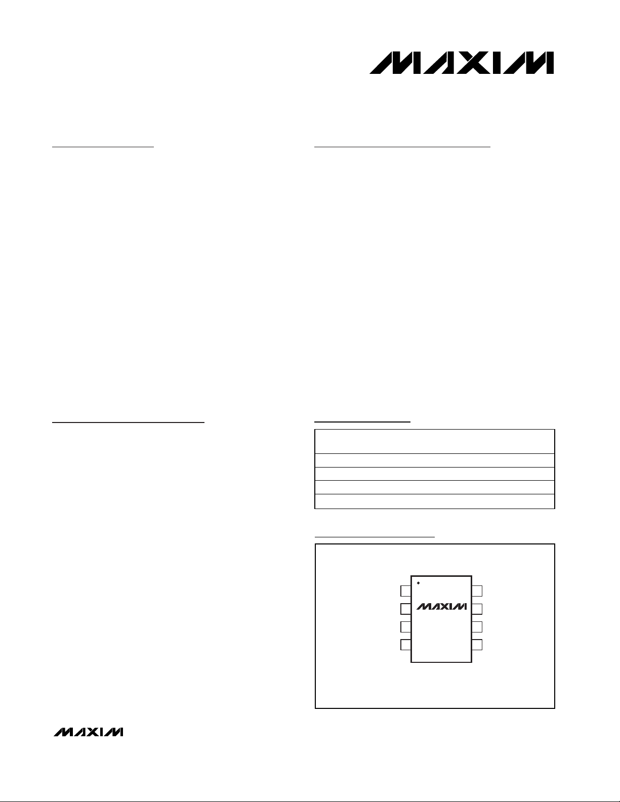
Pin Configuration
19-2036; Rev 0; 5/01
For pricing, delivery, and ordering information, please contact Maxim/Dallas Direct! at
1-888-629-4642, or visit Maxim’s website at www.maxim-ic.com.
Ordering Information
AutoShutdown is a trademark of Maxim Integrated Products.
SPI and QSPI are trademarks of Motorola Inc.
MICROWIRE is a trademark of National Semiconductor Corp.
PART
MAX1086EKA-T -40°C to +85°C 8 SOT23 AAEZ
MAX1087EKA-T -40°C to +85°C 8 SOT23 AAEV
MAX1088EKA-T -40°C to +85°C 8 SOT23 AAFB
MAX1089EKA-T -40°C to +85°C 8 SOT23 AAEX
TEMP.
RANGE
PIN-
PACKAGE
TOP
MARK
TOP VIEW
1
V
DD
2
MAX1086
MAX1087
AIN2 (AIN-)
( ) ARE FOR THE MAX1088/MAX1089
3
4
MAX1088
MAX1089
SOT23-8
87SCLK
DOUTAIN1 (AIN+)
CNVST
6
REFGND
5
Page 2
MAX1086–MAX1089
150ksps, 10-Bit, 2-Channel Single-Ended, and
1-Channel True-Differential ADCs in SOT23
2 _______________________________________________________________________________________
ABSOLUTE MAXIMUM RATINGS
ELECTRICAL CHARACTERISTICS
(VDD= +2.7V to +3.6V, V
REF
= +2.5V for MAX1087/MAX1089, or VDD = +4.75V to +5.25V, V
REF
= +4.096V for MAX1086/MAX1088,
0.1µF capacitor at REF, f
SCLK
= 8MHz (50% duty cycle), AIN- = GND for MAX1088/MAX1089. TA= T
MIN
to T
MAX,
unless otherwise
noted. Typical values at T
A
= +25°C.)
Stresses beyond those listed under “Absolute Maximum Ratings” may cause permanent damage to the device. These are stress ratings only, and functional
operation of the device at these or any other conditions beyond those indicated in the operational sections of the specifications is not implied. Exposure to
absolute maximum rating conditions for extended periods may affect device reliability.
VDDto GND.............................................................-0.3V to +6V
CNVST, SCLK, DOUT to GND......................-0.3V to (V
DD
+0.3V)
REF, AIN1(AIN+), AIN2(AIN-) to GND..........-0.3V to (V
DD
+0.3V)
Maximum Current Into Any Pin ...........................................50mA
Continuous Power Dissipation (T
A
= +70°C)
8-Pin SOT23(derate 9.70mW/°C above T
A
= +70°C) ....777mW
Operating Temperature Ranges.........................-40°C to +85°C
Storage Temperature Range .............................-60°C to +150°C
Lead Temperature (soldering, 10s) .................................+300°C
DC ACCURACY (Note 1)
Resolution 10 Bits
Relative Accuracy (Note 2) INL ±1.0 LSB
Differential Nonlinearity DNL No missing codes over temperature ±1.0 LSB
Offset Error ±0.5 ±1.0 LSB
Gain Error (Note 3) ±1.0 ±2.0 LSB
Gain Temperature Coefficient ±0.8 ppm/°C
Channel-to-Channel Offset
Channel-to-Channel Gain Matching ±0.1 LSB
Input Common-Mode Rejection CMR VCM = 0V to VDD; zero scale input ±0.1 mV
DYNAMIC SPECIFICATIONS: (f
for MAX1087/MAX1089, 150ksps, f
Signal to Noise Plus Distortion SINAD 61 dB
Total Harmonic Distortion
(up to the 5
Spurious-Free Dynamic Range SFDR 70 dB
Full-Power Bandwidth -3dB point 1 MHz
Full-Linear Bandwidth SINAD>56dB 100 kHz
CONVERSION RATE
Conversion Time t
T/H Acquisition Time t
Aperture Delay 30 ns
Aperture Jitter <50 ps
Maximum Serial Clock Frequency f
Duty Cycle 30 70 %
PARAMETER SYMBOL CONDITIONS MIN TYP MAX UNITS
th
harmonic)
(sine-wave) = 10kHz, VIN = 4.096Vp-p for MAX1086/MAX1088 or VIN = 2.5V
IN
= 8MHZ, AIN- = GND for MAX1088/MAX1089)
SCLK
THD -70 dB
CONV
ACQ
SCLK
±0.1 LSB
8 MHz
PP
3.7 µs
1.4 µs
Page 3
MAX1086–MAX1089
150ksps, 10-Bit, 2-Channel Single-Ended, and
1-Channel True-Differential ADCs in SOT23
_______________________________________________________________________________________ 3
ELECTRICAL CHARACTERISTICS (continued)
(VDD= +2.7V to +3.6V, V
REF
= +2.5V for MAX1087/MAX1089, or VDD
= +4.75V to +5.25V, V
REF
= +4.096V for MAX1086/MAX1088,
0.1µF capacitor at REF, f
SCLK
= 8MHz (50% duty cycle), AIN- = GND for MAX1088/MAX1089. TA= T
MIN
to T
MAX,
unless otherwise
noted. Typical values at T
A
= +25°C.)
PARAMETER SYMBOL CONDITIONS MIN TYP MAX UNITS
ANALOG INPUT
Input Voltage Range (Note 4)
Unipolar 0 V
Bipolar -V
Input Leakage Current C hannel not sel ected or conver si on stop p ed ±0.01 ±1 µA
Input Capacitance 34 pF
EXTERNAL REFERENCE INPUT
Input Voltage Range V
Input Current I
REF
REF
V
= +2.5V at 150ksps 16 30
REF
V
= +4.096V at 150ksps 26 45
REF
Acquisition/Between conversions ±0.01 ±1
DIGITAL INPUTS/OUTPUT (SCLK, CNVST, DOUT)
Input Low Voltage V
Input High Voltage V
Input Leakage Current I
Input Capacitance C
Output Low Voltage V
Output High Voltage V
Three-State Leakage Current I
Three-State Output Capacitance C
IL
IH
L
IN
OL
OH
L
OUT
I
= 2mA 0.4 V
SINK
I
= 4mA 0.8 V
SINK
I
SOURCE
= 1.5mA
CNVST = GND ±10 µA
CNVST = GND 15 pF
POWER REQUIREMENTS
Positive Supply Voltage V
DD
MAX1086/MAX1088 4.75 5.0 5.25
MAX1087/MAX1089 2.7 3.0 3.6
VDD = +3V
Positive Supply Current I
DD
VDD = +5V
Shutdown 0.2 5
Positive Supply Rejection PSR
VDD = 5V ±5%; full-scale input ±0.1 1.0
= +2.7V to +3.6V; full-scale input ±0.1 ±1.2
V
DD
f
f
f
f
f
f
f
f
=150ksps 245 350
SAMPLE
=100ksps 150
SAMPLE
=10ksps 15
SAMPLE
=1ksps 2
SAMPLE
=150ksps 320 400
SAMPLE
=100ksps 215
SAMPLE
=10ksps 22
SAMPLE
=1ksps 2.5
SAMPLE
REF
1.0
/2 V
REF
/2
REF
V
DD
+50mV
0.8 V
V
-1 V
DD
±0.1 µA
15 pF
V
DD
-0.5
V
V
µA
V
V
µA
mV
Page 4
MAX1086–MAX1089
150ksps, 10-Bit, 2-Channel Single-Ended, and
1-Channel True-Differential ADCs in SOT23
4 _______________________________________________________________________________________
TIMING CHARACTERISTICS (Figures 1 and 2)
(VDD= +2.7V to +3.6V, V
REF
= +2.5V for MAX1087/MAX1089, or VDD= +4.75V to +5.25V, V
REF
= +4.096V for MAX1086/MAX1088,
0.1µF capacitor at REF, f
SCLK
= 8MHz (50% duty cycle); AIN- = GND for MAX1088/MAX1089. TA= T
MIN
to T
MAX,
unless otherwise
noted. Typical values at T
A
= +25°C.)
Note 1: Unipolar input.
Note 2: Relative accuracy is the deviation of the analog value at any code from its theoretical value after offset and gain errors have
been removed.
Note 3: Offset nulled.
Note 4: The absolute input range for the analog inputs is from GND to V
DD
.
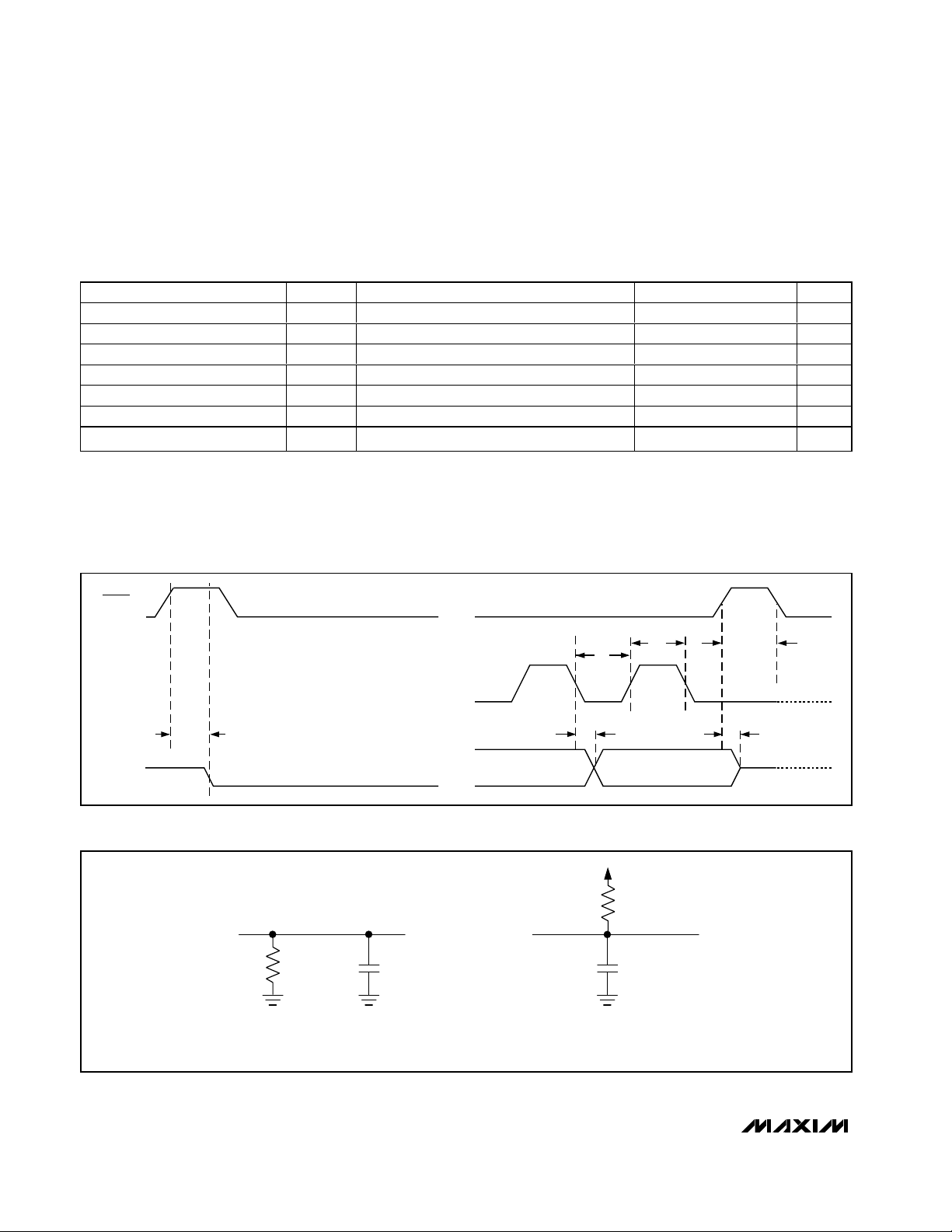
Figure 1. Detailed Serial-Interface Timing Sequence
Figure 2. Load Circuits for Enable/Disable Times
PARAMETERS SYMBOL CONDITIONS MIN TYP MAX UNITS
SCLK Pulse Width High t
SCLK Pulse Width Low t
SCLK Fall to DOUT Transition t
SCLK Rise to DOUT Disable t
CNVST Rise to DOUT Enable t
CNVST Fall to MSB Valid t
CNVST Pulse Width t
CH
CL
C
DOT
DOD
DOE
DOV
CSW
= 30pF 60 ns
LOAD
C
= 30pF 100 500 ns
LOAD
C
= 30pF 80 ns
LOAD
C
= 30pF 3.7 µs
LOAD
38 ns
38 ns
30 ns
CNVST
SCLK
t
DOE
HIGH-Z
DOUT
DOUT
6kΩ
GND
a) HIGH -Z TO VOH, VOL TO VOH, AND VOH TO HIGH -Z
• • •
t
V
t
DOT
DD
C
GND
CH
L
t
CL
• • •
• • •
6kΩ
DOUT
C
L
a) HIGH -Z TO V
, VOH TO VOL, AND VOL TO HIGH -Z
OL
t
CSW
t
DOD
HIGH-Z
Page 5
MAX1086–MAX1089
150ksps, 10-Bit, 2-Channel Single-Ended, and
1-Channel True-Differential ADCs in SOT23
_______________________________________________________________________________________ 5
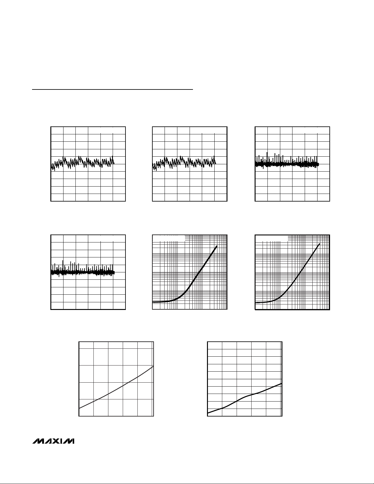
Typical Operating Characteristics
(VDD= +3.0V, V
REF
= +2.5V for MAX1087/MAX1089 or VDD= +5.0V, V
REF
= +4.096V for MAX1086/MAX1088, 0.1µF capacitor at
REF, f
SCLK
= 8MHz, (50% Duty Cycle), AIN- = GND for MAX1088/1089, TA= +25°C, unless otherwise noted.)
INTEGRAL NONLINEARITY
vs. OUTPUT CODE
1.0
0.8
0.6
0.4
0.2
0
INL (LSB)
-0.2
-0.4
-0.6
-0.8
-1.0
0 400200 600 800 1000 1200
OUTPUT CODE
DIFFERENTIAL NONLINEARITY
vs. OUTPUT CODE
1.0
0.8
0.6
0.4
0.2
0
DNL (LSB)
-0.2
-0.4
-0.6
-0.8
-1.0
0 400 600200 800 1000 1200
OUTPUT CODE
380
330
280
SUPPLY CURRENT ( µA)
230
180
2.7 3.73.2 4.2 4.7 5.2
MAX1087/MAX1089
MAX1086-9 toc01
MAX1086/MAX1088
MAX1086-9 toc04
SUPPLY CURRENT
vs. SUPPLY VOLTAGE
VDD (V)
INTEGRAL NONLINEARITY
vs. OUTPUT CODE
1.0
0.8
0.6
0.4
0.2
0
INL (LSB)
-0.2
-0.4
-0.6
-0.8
-1.0
0 400200 600 800 1000 1200
SUPPLY CURRENT
vs. SAMPLING RATE
1000
MAX1087/MAX1089
100
10
SUPPLY CURRENT (µA)
1
0.1
0.001 10 1000
MAX1086-9 toc07
1.0
SAMPLING RATE (ksps)
MAX1086/MAX1088
OUTPUT CODE
SHUTDOWN CURRENT (nA)
0.50
0.45
0.40
0.35
0.30
0.25
0.20
0.15
0.10
0.05
0
2.7 3.73.2 4.2 4.7 5.2
1.0
0.8
0.6
MAX1086-9 toc02
0.4
0.2
0
DNL (LSB)
-0.2
-0.4
-0.6
-0.8
-1.0
0 400 600200 800 1000 1200
1000
MAX1086/MAX1088
MAX1086-9 toc05
100
10
SUPPLY CURRENT (µA)
1
0.1
0.001 10 10001.0
SHUTDOWN CURRENT
vs. SUPPLY VOLTAGE
VDD (V)
DIFFERENTIAL NONLINEARITY
vs. OUTPUT CODE
MAX1087/MAX1089
MAX1086-9 toc03
OUTPUT CODE
SUPPLY CURRENT
vs. SAMPLING RATE
MAX1086-9 toc06
SAMPLING RATE (ksps)
MAX1086-9 toc08
Page 6

MAX1086–MAX1089
150ksps, 10-Bit, 2-Channel Single-Ended, and
1-Channel True-Differential ADCs in SOT23
6 _______________________________________________________________________________________
Typical Operating Characteristics (continued)
(VDD= 3.0V, V
REF
= 2.5V for MAX1087/MAX1089 or VDD= 5.0V, V
REF
= +4.096V for MAX1086MAX1088, 0.1µF capacitor at REF,
f
SCLK
= 8MHz, (50% Duty Cycle), AIN- = GND for MAX1088/89, TA= +25°C, unless otherwise noted.)
0
100
50
250
200
150
300
-40 0 20-20 40 60 80
SHUTDOWN CURRENT
vs. TEMPERATURE
MAX1086-9 toc10
TEMPERATURE (°C)
SHUTDOWN CURRENT (nA)
-1.00
-0.40
0.60
-0.80
0.00
-0.20
0.80
0.60
0.40
0.20
1.00
-40 -20 0 20 40 60 80
OFFSET ERROR
vs. TEMPERATURE
MAX1086-9 toc11
TEMPERATURE (°C)
OFFSET ERROR (LSB)
-1.0
-0.6
-0.8
-0.2
-0.4
0.2
0.4
0.6
0.8
0
1.0
2.7 3.7 4.23.2 4.7 5.2
OFFSET ERROR
vs. SUPPLY VOLTAGE
MAX1086-9 toc12
VDD (V)
OFFSET ERROR (LSB)
-40 0 20-20 40 60 80
GAIN ERROR
vs. TEMPERATURE
MAX1086-9 toc13
TEMPERATURE (°C)
GAIN ERROR (LSB)
-1.0
-0.6
-0.8
-0.2
-0.4
0.2
0.4
0.6
0.8
0
1.0
2.7 3.73.2 4.2 4.7 5.2
GAIN ERROR
vs. SUPPLY VOLTAGE
MAX1086-9 toc14
VDD (V)
GAIN ERROR (LSB)
-1.0
-0.6
-0.8
-0.2
-0.4
0.2
0.4
0.6
0.8
0
1.0
-140.00
-120.00
-100.00
-80.00
-60.00
-40.00
-20.00
0.00
20.00
03015 45 60
FFT PLOT (SINAD)
MAX1086-9 toc15
FREQUENCY (kHz)
AMPLITUDE (dB)
180
280
230
330
380
-40 0-20 20 40 60 80
SUPPLY CURRENT
vs. TEMPERATURE
MAX1086-9 toc09
TEMPERATURE (°C)
SUPPLY CURRENT (µA)
Page 7

MAX1086–MAX1089
150ksps, 10-Bit, 2-Channel Single-Ended, and
1-Channel True-Differential ADCs in SOT23
_______________________________________________________________________________________ 7
Detailed Description
The MAX1086–MAX1089 analog-to-digital converters
(ADCs) use a successive-approximation conversion
(SAR) technique and an on-chip track-and-hold (T/H)
structure to convert an analog signal into a 10-bit digital
result.
The serial interface provides easy interfacing to microprocessors (µPs). Figure 3 shows the simplified internal
structure for the MAX1086/MAX1087 (2–channels, single-ended) and the MAX1088/MAX1089 (1–channel,
true-differential).
True-Differential Analog Input Track/Hold
The equivalent circuit of Figure 4 shows the
MAX1086–MAX1089’s input architecture which is composed of a T/H, input multiplexer, comparator, and
switched-capacitor DAC. The T/H enters its tracking
mode on the rising edge of CNVST. The positive input
capacitor is connected to AIN1 or AIN2 (MAX1086/
MAX1087) or AIN+ (MAX1088/MAX1089). The negative
input capacitor is connected to GND (MAX1086/
MAX1087) or AIN- (MAX1088/MAX1089). The T/H
enters its hold mode on the falling edge of CNVST and
the difference between the sampled positive and negative input voltages is converted. The time required for
the T/H to acquire an input signal is determined by how
quickly its input capacitance is charged. If the input
signal’s source impedance is high, the acquisition time
lengthens, and CNVST must be held high for a longer
period of time. The acquisition time, t
ACQ
, is the maximum time needed for the signal to be acquired, plus
the power-up time. It is calculated by the following
equation:
t
ACQ
= 7 x (RS+ RIN) x 24pF + t
PWR
Pin Description
Figure 3. Simplified Functional Diagram
NAME
PIN
MAX1086
MAX1087
1VDDV
2 AIN1 AIN+ Analog Input Channel 1 (MAX1086/MAX1087) or Positive Analog Input (MAX1088/MAX1089)
3 AIN2 AIN- Analog Input Channel 2 (MAX1086/MAX1087) or Negative Analog Input (MAX1088/MAX1089)
4 GND GND Ground
5 REF REF
6 CNVST CNVST
7 DOUT DOUT
8 SCLK SCLK Serial Clock Input. Clocks out data at DOUT MSB first.
MAX1088
MAX1089
DD
Positive Supply Voltage. +2.7V to +3.6V (MAX1087/MAX1089); +4.75V to +5.25V
(MAX1086/MAX1088). Bypass with a 0.1µF capacitor to GND.
External Reference Voltage Input. Sets the analog voltage range. Bypass with a 0.1µF
capacitor to GND.
Conversion Start. A rising edge powers-up the IC and places it in track mode. At the falling
edge of CNVST, the device enters hold mode and begins conversion. CNVST also selects the
input channel (MAX1086/MAX1087) or input polarity (MAX1088/MAX1089).
Serial Data Output. DOUT transitions the falling edge of SCLK. DOUT goes low at the start of a
conversion and presents the MSB at the completion of a conversion. DOUT goes highimpedance once data has been fully clocked out.
FUNCTION
MAX1086–MAX1089
OSCILLATOR
CNVST
SCLK
INPUT SHIFT
REGISTER
CONTROL
AIN1
(AIN+)
AIN2
(AIN-)
REF
T/H
10-BIT
SAR
ADC
DOUT
( ) ARE FOR MAX1088/MAX1089
Page 8

MAX1086–MAX1089
150ksps, 10-Bit, 2-Channel Single-Ended, and
1-Channel True-Differential ADCs in SOT23
8 _______________________________________________________________________________________
where RIN= 1.5kΩ, RSis the source impedance of the
input signal, and t
PWR
= 1µs is the power-up time of the
device.
Note: t
ACQ
is never less than 1.4µs and any source
impedance below 300Ω does not significantly affect the
ADC‘s AC performance. A high impedance source can
be accommodated either by lengthening t
ACQ
or by
placing a 1µF capacitor between the positive and negative analog inputs.
Selecting AIN1 or AIN2
(MAX1086/MAX1087)
Select between the MAX1086/MAX1087’s two positive
input channels using the CNVST pin. If AIN1 is desired
(Figure 5a), drive CNVST high to power-up the ADC
and place the T/H in track mode with AIN1 connected
to the positive input capacitor. Hold CNVST high for
t
ACQ
to fully acquire the signal. Drive CNVST low to
place the T/H in hold mode. The ADC will then perform
a conversion and shutdown automatically. The MSB is
available at DOUT after 3.7µs. Data can then be
clocked out using SCLK. Be sure to clock out all 12 bits
of data (the 10-bit result plus two sub-bits) before driving CNVST high for the next conversion. If all 12 bits of
data are not clocked out before CNVST is driven high,
AIN2 will be selected for the next conversion.
If AIN2 is desired (Figure 5b), drive CNVST high for at
least 30ns. Next, drive it low for at least 30ns, and then
high again. This will power-up the ADC and place the
T/H in track mode with AIN2 connected to the positive
input capacitor. Now hold CNVST high for t
ACQ
to fully
acquire the signal. Drive CNVST low to place the T/H in
hold mode. The ADC will then perform a conversion
and shutdown automatically. The MSB is available at
DOUT after 3.7µs. Data can then be clocked out using
SCLK. If all 12 bits of data are not clocked out before
CNVST is driven high, AIN2 will be selected for the next
conversion.
Selecting Unipolar or Bipolar Conversions
(MAX1088/MAX1089)
Initiate true-differential conversions with the
MAX1088/MAX1089’s unipolar and bipolar modes,
using the CNVST pin. AIN+ and AIN- are sampled at
the falling edge of CNVST. In unipolar mode, AIN+ can
exceed AIN- by up to V
REF
. The output format is
straight binary. In bipolar mode, either input can
exceed the other by up to V
REF
/2. The output format is
two’s complement.
Note: In both modes, AIN+ and AIN- must not exceed
VDDby more than 50mV or be lower than GND by more
than 50mV.
If unipolar mode is desired (Figure 5a), drive CNVST
high to power-up the ADC and place the T/H in track
mode with AIN+ and AIN- connected to the input
capacitors. Hold CNVST high for t
ACQ
to fully acquire
the signal. Drive CNVST low to place the T/H in hold
mode. The ADC will then perform a conversion and
shutdown automatically. The MSB is available at DOUT
after 3.7µs. Data can then be clocked out using SCLK.
Be sure to clock out all 12 bits (the 10-bit result plus
two sub-bits) of data before driving CNVST high for the
next conversion. If all 12 bits of data are not clocked
out before CNVST is driven high, bipolar mode will be
selected for the next conversion.
If bipolar mode is desired (Figure 5b), drive CNVST
high for at least 30ns. Next, drive it low for at least 30ns
and then high again. This will place the T/H in track
mode with AIN+ and AIN- connected to the input
capacitors. Now hold CNVST high for t
ACQ
to fully
acquire the signal. Drive CNVST low to place the T/H in
hold mode. The ADC will then perform a conversion
and shutdown automatically. The MSB is available at
DOUT after 3.7µs. Data can then be clocked out using
SCLK. If all 12 bits of data are not clocked out before
CNVST is driven high, bipolar mode will be selected for
the next conversion.
Input Bandwidth
The ADCs input tracking circuitry has a 1MHz smallsignal bandwidth, so it is possible to digitize highspeed transient events and measure periodic signals
with bandwidths exceeding the ADC’s sampling rate by
using undersampling techniques. To avoid high frequency signals being aliased into the frequency band
of interest, anti-alias filtering is recommended.
Figure 4. Equivalent Input Circuit
AIN2
AIN1(AIN+)
HOLD
GND(AIN-)
*( ) APPLIES TO MAX1088/1089
REF
GND
CIN+
CIN-
HOLD
V
DD
DAC
COMPARATOR
+
-
RIN-
/2
RIN+
HOLD
TRACK
Page 9

MAX1086–MAX1089
150ksps, 10-Bit, 2-Channel Single-Ended, and
1-Channel True-Differential ADCs in SOT23
_______________________________________________________________________________________ 9
Analog Input Protection
Internal protection diodes which clamp the analog input
to VDDand GND allow the analog input pins to swing
from GND - 0.3V to VDD+ 0.3V without damage. Both
inputs must not exceed VDDby more than 50mV or be
lower than GND by more than 50mV for accurate conversions. If an off-channel analog input voltage exceeds
the supplies, limit the input current to 2mA.
Internal Clock
The MAX1086–MAX1089 operate from an internal oscillator, which is accurate within 10% of the 4MHz specified
clock rate. This results in a worse case conversion time
of 3.7µs. The internal clock releases the system microprocessor from running the SAR conversion clock and
allows the conversion results to be read back at the
processor’s convenience, at any clock rate from 0 to
8MHz.
Figure 5b. Single Conversion AIN2 vs. GND (MAX1086/MAX1087), bipolar mode AIN+ vs. AIN- (MAX1088/MAX1089)
Figure 5a. Single Conversion AIN1 vs. GND (MAX1086/MAX1087), unipolar mode AIN+ vs. AIN- (MAX1088/MAX1089)
t
CONV
CNVST
t
ACQ
SCLK
DOUT
HIGH-Z
t
t
ACQ
CNVST
SCLK
DOUT
HIGH-Z
B9
MSB
SAMPLING INSTANT
CONV
B9
MSB
B8 B7 B6 B5
B8 B7 B6 B5
41812
B4
B3 B2 B1
41812
B4
B3 B2 B1
B0
LSB
B0
LSB
S1 S0
S1 S0
HIGH-Z
HIGH-Z
SAMPLING INSTANT
Page 10

MAX1086–MAX1089
150ksps, 10-Bit, 2-Channel Single-Ended, and
1-Channel True-Differential ADCs in SOT23
10 ______________________________________________________________________________________
Output Data Format
Figures 5a and 5b illustrate the conversion timing for
the MAX1086–MAX1089. The 10-bit conversion result is
output in MSB first format, followed by two sub-bits (S1
and S0). Data on DOUT transitions on the falling edge
of SCLK. All 12-bits must be clocked out before CNVST
transitions again. For the MAX1088/MAX1089, data is
straight binary for unipolar mode and two’s complement for bipolar mode. For the MAX1086/MAX1087,
data is always straight binary.
Applications Information
Automatic Shutdown Mode
With CNVST low, the MAX1086–MAX1089 defaults to an
AutoShutdown state (<0.2µA) after power-up and
between conversions. After detecting a rising edge on
CNVST, the part powers up, sets DOUT low and enters
track mode. After detecting a falling-edge on CNVST, the
device enters hold mode and begins the conversion. A
maximum of 3.7µs later, the device completes conversion, enters shutdown and MSB is available at DOUT.
External Reference
An external reference is required for the MAX1086–
MAX1089. Use a 0.1µF bypass capacitor for best performance. The reference input structure allows a voltage range of +1V to VDD+ 50mV.
Transfer Function
Figure 6 shows the unipolar transfer function for the
MAX1086–MAX1089. Figure 7 shows the bipolar transfer
function for the MAX1088/MAX1089. Code transitions
occur halfway between successive-integer LSB values.
Connection to Standard Interfaces
The MAX1086–MAX1089 feature a serial interface that is
fully compatible with SPI, QSPI, and MICROWIRE. If a
serial interface is available, establish the CPU’s serial
interface as a master, so that the CPU generates the serial clock for the ADCs. Select a clock frequency up to
8MHz.
How to Perform a Conversion
1) Use a general purpose I/O line on the CPU to hold
CNVST low between conversions.
2) Drive CNVST high to acquire AIN1(MAX1086/
MAX1087) or unipolar mode (MAX1088/MAX1089).
To acquire AIN2(MAX1086/MAX1087) or bipolar
mode (MAX1088/MAX1089), drive CNVST low and
high again.
3) Hold CNVST high for 1.4µs.
4) Drive CNVST low and wait approximately 3.7µs for
conversion to complete. After 3.7µs, the MSB is
available at DOUT.
5) Activate SCLK for a minimum of 12 rising clock
edges. DOUT transitions on SCLK’s falling edge
Figure 6. Unipolar Transfer Function
Figure 7. Bipolar Transfer Function
OUTPUT CODE
11 . . . 111
11 . . . 110
11 . . . 101
00 . . . 011
00 . . . 010
00 . . . 001
00 . . . 000
0
123
FULL-SCALE
TRANSITION
INPUT VOLTAGE (LSB)
MAX1086–
MAX1089
FS = V
ZS = GND
1LSB =
FS
FS - 3/2LSB
REF
V
1024
REF
011 . . . 111
011 . . . 110
000 . . . 010
000 . . . 001
000 . . . 000
111 . . . 111
111 . . . 110
111 . . . 101
100 . . . 001
100 . . . 000
*V
COM
OUTPUT CODE
FS
ZS = 0
-FS =
1LSB =
- FS
≤
V
/ 2 *VIN = (AIN+) - (AIN-)
REF
V
REF
=
2
-V
REF
2
V
REF
1024
INPUT VOLTAGE (LSB)
0
MAX1088/MAX1089
+FS - 1LSB
Page 11

and is available in MSB-first format. Observe the
SCLK to DOUT valid timing characteristic. Clock
data into the µP on SCLK’s rising-edge.
SPI and MICROWIRE Interface
When using SPI interface (Figure 8a) or MICROWIRE
(Figure 8a and 8b), set CPOL = CPHA = 0. Two 8-bit
readings are necessary to obtain the entire 10-bit result
from the ADC. DOUT data transitions on the serial
clock’s falling edge and is clocked into the µP on
SCLK’s rising edge. The first 8-bit data stream contains
the first 8-bits of DOUT starting with the MSB. The second 8-bit data stream contains the remaining two result
bits (B1, B0) and two trailing sub-bits (S1, S0). DOUT
then goes high impedance.
QSPI Interface
Using the high-speed QSPI interface (Figure 9a) with
CPOL = 0 and CPHA = 0, the MAX1086–MAX1089
support a maximum f
SCLK
of 8MHz. One 8- to16-bit
reading is necessary to obtain the entire 10-bit result
from the ADC. DOUT data transitions on the serial
clock’s falling edge and is clocked into the µP on
SCLK’s rising edge. The first 10 bits are the data and
the next two bits are sub-bits (S1, S0). DOUT then
goes high impedance (Figure 9b).
PIC16 and SSP Module and
PIC17 Interface
The MAX1086–MAX1089 are compatible with a
PIC16/PIC17 microcontroller (µC), using the synchronous serial port (SSP) module
To establish SPI communication, connect the controller
as shown in Figure 10a and configure the PIC16/PIC17
as system master. This is done by initializing its synchronous serial port control register (SSPCON) and
synchronous serial port status register (SSPSTAT) to
the bit patterns shown in Tables 1 and 2.
In SPI mode, the PIC16/PIC17 µCs allow eight bits of
data to be synchronously transmitted and received
simultaneously. Two consecutive 8-bit readings (Figure
10b) are necessary to obtain the entire 10-bit result
from the ADC. DOUT data transitions on the serial
clock’s falling edge and is clocked into the µC on
SCLK’s rising edge. The first 8-bit data stream contains
MAX1086–MAX1089
150ksps, 10-Bit, 2-Channel Single-Ended, and
1-Channel True-Differential ADCs in SOT23
______________________________________________________________________________________ 11
Figure 8a. SPI Connections Figure 8b. MICROWIRE Connections
Table 1. Detailed SSPCON Register Content
SPI
SCK
MISO
I/O
V
DD
SS
CNVST
SCLK
DOUT
MAX1086–
MAX1089
I/O
SK
SI
MICROWIRE
CNVST
SCLK
DOUT
MAX1086–
MAX1089
CONTROL BIT
WCOL Bit 7 X Write Collision Detection Bit
SSPOV Bit 6 X Receive Overflow Detect Bit
SSPEN Bit 5 1
CKP Bit 4 0 Clock Polarity Select Bit. CKP = 0 for SPI master mode selection.
SSPM3 Bit 3 0
SSPM2 Bit 2 0
SSPM1 Bit 1 0
SSPM0 Bit 0 1
X = Don’t care
MAX1086–MAX1089
SETTINGS
SYNCHRONOUS SERIAL PORT CONTROL REGISTER (SSPCON)
Synchronous Serial Port Enable Bit.
0: Disables serial port and configures these pins as I/O port pins.
1: Enables serial port and configures SCK, SDO and SCI pins as serial port pins.
Synchronous Serial Port Mode Select Bit. Sets SPI master mode and selects
= f
OSC
/ 16.
f
CLK
Page 12

MAX1086–MAX1089
the first eight data bits starting with the MSB. The second 8-bit data stream contains the remaining bits, D1
through D0, and the two sub-bits S1 and S0.
Layout, Grounding, and Bypassing
For best performance, use printed circuit (PC) boards.
Wire-wrap configurations are not recommended since
the layout should ensure proper separation of analog
and digital traces. Do not run analog and digital lines
parallel to each other, and do not lay out digital signal
paths underneath the ADC package. Use separate
analog and digital PC board ground sections with only
one starpoint (Figure 11), connecting the two ground
systems (analog and digital). For lowest-noise operation, ensure the ground return to the star ground’s
power supply is low impedance and as short as possible. Route digital signals far away from sensitive analog
and reference inputs.
High-frequency noise in the power supply (VDD) may
degrade the performance of the ADC’s fast comparator.
Bypass V
DD
to the star ground with a 0.1µF capacitor,
located as close as possible to the MAX1086–MAX1089s
power supply pin. Minimize capacitor lead length for best
supply-noise rejection. Add an attenuation resistor (5Ω) if
the power supply is extremely noisy.
150ksps, 10-Bit, 2-Channel Single-Ended, and
1-Channel True-Differential ADCs in SOT23
12 ______________________________________________________________________________________
Figure 9a. QSPI Connections
Table 2. Detailed SSPSTAT Register Content
Figure 8c. SPI/MICROWIRE Interface Timing Sequence (CPOL = CPHA = 0)
CNVST
1ST BYTE READ
2ND BYTE READ
SCLK
DOUT
B9
B8 B7 B6 B5
MSB
SAMPLING INSTANT
418
B4
B3 B2 B1
CNVST
SCLK
DOUT
MAX1086–
MAX1089
QSPI
SCK
MISO
CS
V
DD
SS
B0
LSB
S1 S0
12
HIGH-Z
16
CONTROL BIT
SMP Bit 7 0
CKE Bit 6 1 SPI Clock Edge Select Bit. Data will be transmitted on the rising edge of the serial clock.
D/A
P Bit 4 X Stop Bit
S Bit 3 X
R/W
UA Bit 1 X
BF Bit 0 X
X = Don’t care
MAX1086–MAX1089
SETTINGS
SPI Data Input Sample Phase. Input data is sampled at the middle of the data output
time.
Bit 5 X Data Address Bit
Start Bit
Bit 2 X
Read/Write Bit Information
Update Address
Buffer Full Status Bit
SYNCHRONOUS SERIAL STATUS REGISTER (SSPSTAT)
Page 13

Definitions
Integral Nonlinearity
Integral nonlinearity (INL) is the deviation of the values
on an actual transfer function from a straight line. This
straight line can be either a best-straight-line fit or a line
drawn between the endpoints of the transfer function,
once offset and gain errors have been nullified. The static linearity parameters for the MAX1086–MAX1089 are
measured using the endpoint method.
Differential Nonlinearity
Differential nonlinearity (DNL) is the difference between
an actual step-width and the ideal value of 1LSB. A
DNL error specification of less than 1LSB guarantees
no missing codes and a monotonic transfer function.
MAX1086–MAX1089
150ksps, 10-Bit, 2-Channel Single-Ended, and
1-Channel True-Differential ADCs in SOT23
______________________________________________________________________________________ 13
Figure 9b. QSPI Interface Timing Sequence (CPOL = CPHA = 0)
Figure 10a. SPI Interface Connection for a PIC16/PIC17 Controller
Figure 10b. SPI Interface Timing with PIC16/PIC17 in Master Mode (CKE = 1, CKP = 0, SMP = 0, SSPM3 - SSPM0 = 0001)
CNVST
SCLK
DOUT
B9
B8 B7 B6 B5
MSB
SAMPLING INSTANT
418
B4
B3 B2 B1
V
DD
SCLK
DOUT
CNVST
SCK
SDI
I/O
PIC16/PIC17
V
DD
MAX1086–
MAX1089
GND GND
16
B0
LSB
S1 S0
12
HIGH-Z
CNVST
SCLK
DOUT
B9
B8 B7 B6 B5
MSB
SAMPLING INSTANT
1ST BYTE READ
418
B4
B3 B2 B1
B0
LSB
S1 S0
2ND BYTE READ
12
HIGH-Z
16
Page 14

MAX1086–MAX1089
150ksps, 10-Bit, 2-Channel Single-Ended, and
1-Channel True-Differential ADCs in SOT23
14 ______________________________________________________________________________________
Aperture Definitions
Aperture jitter (tAJ) is the sample-to-sample variation in
the time between the samples. Aperture delay (tAD) is
the time between the rising edge of the sampling clock
and the instant when an actual sample is taken.
Signal-to-Noise Ratio
For a waveform perfectly reconstructed from digital samples, signal-to-noise ratio (SNR) is the ratio of full-scale
analog input (RMS value) to the RMS quantization error
(residual error). The ideal, theoretical minimum analog-todigital noise is caused by quantization error only and
results directly from the ADC’s resolution (N-bits):
SNR = (6.02
✕ N + 1.76)dB
In reality, there are other noise sources besides quantization noise: thermal noise, reference noise, clock jitter,
etc. SNR is computed by taking the ratio of the RMS
signal to the RMS noise, which includes all spectral
components minus the fundamental, the first five harmonics, and the DC offset.
Signal-to-Noise Plus Distortion
Signal-to-noise plus distortion (SINAD) is the ratio of the
fundamental input frequency’s RMS amplitude to RMS
equivalent of all other ADC output signals.
SINAD (dB) = 20 ✕ log (Signal
RMS
/ Noise
RMS
)
Effective Number of Bits
Effective number of bits (ENOB) indicates the global
accuracy of an ADC at a specific input frequency and
sampling rate. An ideal ADC’s error consists of quantization noise only. With an input range equal to the fullscale range of the ADC, calculate the effective number
of bits as follows:
ENOB = (SINAD - 1.76) / 6.02
Total Harmonic Distortion
Total harmonic distortion (THD) is the ratio of the RMS
sum of the first five harmonics of the input signal to the
fundamental itself. This is expressed as:
where V1is the fundamental amplitude, and V2through
V5are the amplitudes of the 2nd- through 5th-order harmonics.
Spurious-Free Dynamic Range
Spurious-free dynamic range (SFDR) is the ratio of RMS
amplitude of the fundamental (maximum signal component) to the RMS value of the next largest distortion
component.
Chip Information
TRANSISTOR COUNT: 6922
PROCESS: BiCMOS
Figure 11. Power-Supply and Grounding Connections
SUPPLIES
+3V OR +5V
R* = 5Ω
0.1µF
V
DD
*OPTIONAL
GND
MAX1086–
MAX1089
V
LOGIC
= +5V/+3V
CIRCUITRY
GND
DGND+5V/+3V
DIGITAL
20
THD VVVV V=× +++
2
2
log /
2
3
2
4
2
5
1
Page 15

MAX1086–MAX1089
150ksps, 10-Bit, 2-Channel Single-Ended, and
1-Channel True-Differential ADCs in SOT23
Maxim cannot assume responsibility for use of any circuitry other than circuitry entirely embodied in a Maxim product. No circuit patent licenses are
implied. Maxim reserves the right to change the circuitry and specifications without notice at any time.
Maxim Integrated Products, 120 San Gabriel Drive, Sunnyvale, CA 94086 408-737-7600 ____________________ 15
© 2001 Maxim Integrated Products Printed USA is a registered trademark of Maxim Integrated Products.
Package Information
SOT23, 8L.EPS
 Loading...