

Page 1
General Description
The MAX105 is a dual, 6-bit, analog-to-digital converter
(ADC) designed to allow fast and precise digitizing of
in-phase (I) and quadrature (Q) baseband signals. The
MAX105 converts the analog signals of both I and Q
components to digital outputs at 800Msps while achieving a signal-to-noise ratio (SNR) of typically 37dB with
an input frequency of 200MHz, and an integral nonlinearity (INL) and differential nonlinearity (DNL) of ±0.25
LSB. The MAX105 analog input preamplifiers feature a
400MHz, -0.5dB, and a 1.5GHz, -3dB analog input
bandwidth. Matching channel-to-channel performance
is typically 0.04dB gain, 0.1LSB offset, and 0.2 degrees
phase. Dynamic performance is 36.4dB signal-to-noise
plus distortion (SINAD) with a 200MHz analog input signal and a sampling speed of 800MHz. A fully differential comparator design and encoding circuits reduce
out-of-sequence errors, and ensure excellent
metastable performance of only one error per 10
16
clock
cycles.
In addition, the MAX105 provides LVDS digital outputs
with an internal 6:12 demultiplexer that reduces the output data rate to one-half the sample clock rate. Data is
output in two’s complement format. The MAX105 operates from a +5V analog supply and the LVDS output
ports operate at +3.3V. The data converter’s typical
power dissipation is 2.6W. The device is packaged in
an 80-pin, TQFP package with exposed paddle, and is
specified for the extended (-40°C to +85°C) temperature range. For a lower-speed, 400Msps version of the
MAX105, please refer to the MAX107 data sheet.
Applications
VSAT Receivers
WLANs
Test Instrumentation
Communications Systems
Features
♦ Two Matched 6-Bit, 800Msps ADCs
♦ Excellent Dynamic Performance
36.4dB SINAD at f
IN
≈ 200MHz and
f
CLK
≈ 800MHz
♦ Typical INL and DNL: ±0.25LSB
♦ Channel-to-Channel Phase Matching: ±0.2°
♦ Channel-to-Channel Gain Matching: ±0.04dB
♦ 6:12 Demultiplexer reduces the Data Rates to
400MHz
♦ Low Error Rate: 10
16
Metastable States at
800Msps
♦ LVDS Digital Outputs in Two’s Complement
Format
MAX105
Dual, 6-Bit, 800Msps ADC with On-Chip,
Wideband Input Amplifier
________________________________________________________________ Maxim Integrated Products 1
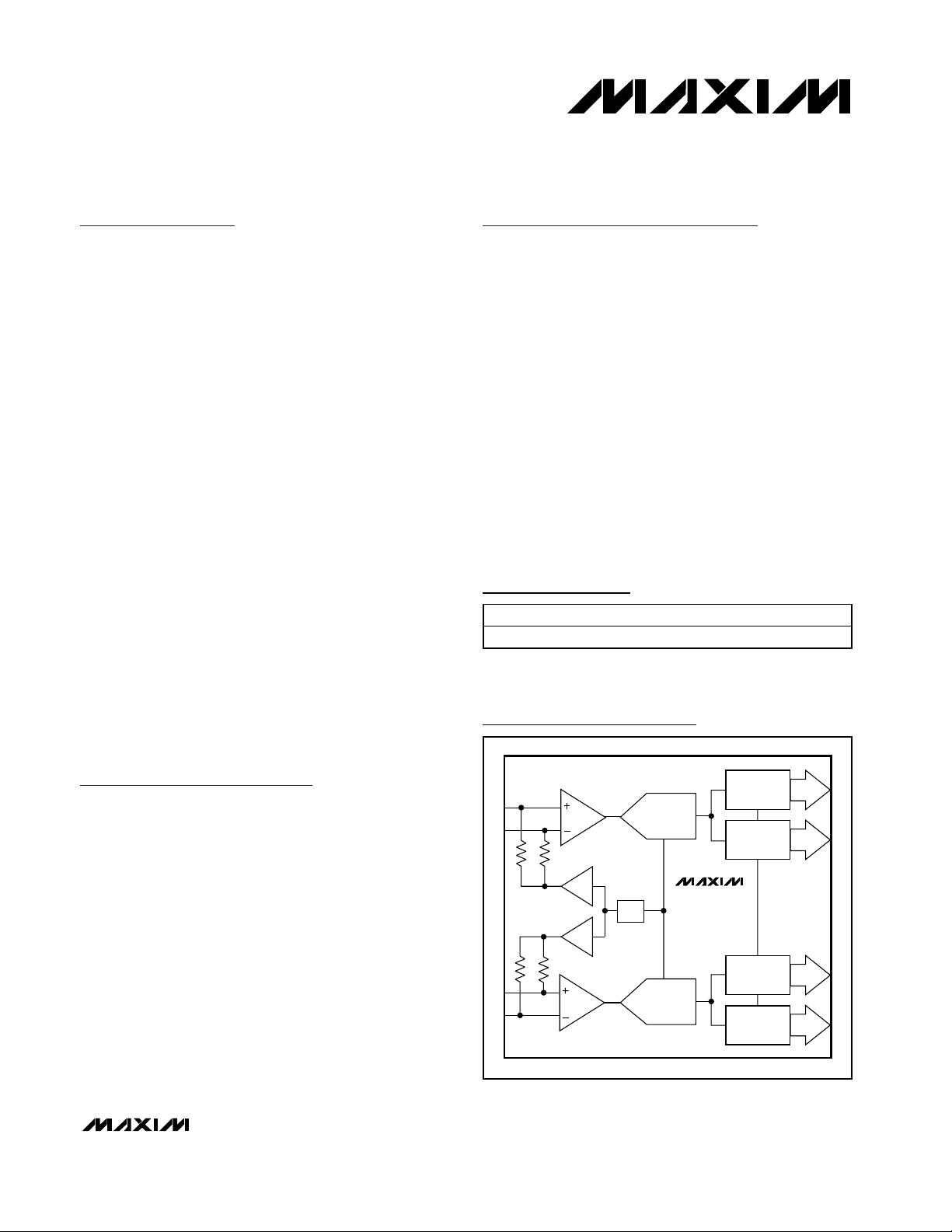
Block Diagram
19-2006; Rev 0; 5/01
Ordering Information
Pin Configuration appears at end of data sheet.
For pricing, delivery, and ordering information, please contact Maxim/Dallas Direct! at
1-888-629-4642, or visit Maxim’s website at www.maxim-ic.com.
PART TEMP. RANGE PIN-PACKAGE
MAX105ECS -40°C to +85°C 80-Pin TQFP-EP
I
PRIMARY
PORT
I
AUXILIARY
PORT
I ADC
REF
Q ADC
MAX107
Q
PRIMARY
PORT
Q
AUXILIARY
PORT
Page 2
MAX105
Dual, 6-Bit, 800Msps ADC with On-Chip,
Wideband Input Amplifier
2 _______________________________________________________________________________________
ABSOLUTE MAXIMUM RATINGS
Stresses beyond those listed under “Absolute Maximum Ratings” may cause permanent damage to the device. These are stress ratings only, and functional
operation of the device at these or any other conditions beyond those indicated in the operational sections of the specifications is not implied. Exposure to
absolute maximum rating conditions for extended periods may affect device reliability.
AVCC, AVCCI, AVCCQ and AVCCR to AGND............-0.3V to +6V
OV
CC
I and OVCCQ to OGND...................................-0.3V to +4V
AGND to OGND ................................................... -0.3V to +0.3V
P0I± to P5I± and A0I± to A5I±
DREADY+, DREADY- to OGNDI .............-0.3V to OV
CC
I+0.3V
P0Q± to P5Q±, A0Q± to A5Q±
DOR+ and DOR- to OGNDQ ................-0.3V to OV
CC
Q+0.3V
REF to AGNDR...........................................-0.3V to AV
CC
R+0.3V
Differential Voltage Between INI+ and INI- ....................-2V, +2V
Differential Voltage Between INQ+ and INQ-.................-2V, +2V
Differential Voltage Between CLK+ and CLK- ...............-2V, +2V
Maximum Current Into Any Pin ...........................................50mA
Continuous Power Dissipation (T
A
= +70°C)
80-Pin TQFP (derate 44mW/°C above +70°C)..................3.5W
Operating Temperature Range
MAX105ECS .....................................................-40°C to +85°C
Junction Temperature......................................................+150°C
Storage Temperature Range .............................-60°C to +150°C
Lead temperature (soldering, 10s) ..................................+300°C
ELECTRICAL CHARACTERISTICS
(AVCC= AVCCI = AVCCQ = AVCCR = +5V, OVCCI = OVCCQ = +3.3V, AGND = AGNDI = AGNDQ = AGNDR = 0, OGNDI = OGNDQ
= 0, f
CLK
= 802.816MHz, CL = 1µF to AGND at REF, RL= 100Ω ±1% applied to digital LVDS outputs, TA= T
MIN
to T
MAX
, unless
otherwise noted. Typical values are at T
A
= +25°C)
DC ACCURACY
Resolution RES 6 Bits
Integral Nonlinearity (Note 1) INL -1 ±0.2 1 LSB
Differential Nonlinearity
(Note 1)
Offset Voltage V
O ffset M atchi ng Betw een AD C s OM (Note 2) -0.5 ±0.1 0.5 LSB
ANALOG INPUTS (INI+, INI-, INQ+, INQ-)
Input Open-Circuit Voltage V
Input Open-Circuit Voltage
Matching
Common Mode Input Voltage
Range (Note 3)
Full-Scale Analog Input
Voltage Range (Note 4)
Input Resistance R
Input Capacitance C
Input Resistance Temperature
Coefficient
Full-Power Analog Input BW FPBW
REFERENCE OUTPUT
Reference Output Resistance R
Reference Output Voltage √REF I
PARAMETER SYMBOL CONDITIONS MIN TYP MAX UNITS
DNL No missing codes guaranteed -1 ±0.25 1 LSB
(Note 2) -1 ±0.25 1 LSB
- V
(V
INI+
Signal + Offset w.r.t. AGND 1.85 3.05 V
IN
Referenced to AGNDR 5 Ω
SOURCE
) - (V
IN-
= 500µA 2.45 2.50 2.55 V
AOC
V
V
FSR
TCR
REF
OS
CM
IN
IN
-0.5dB
- V
INQ+
) ±7.5 mV
INQ-
2.4 2.5 2.6 V
0.76 0.8 0.84 V
1.7 2 kΩ
1.5 pF
150 ppm/°C
400 MHz
p-p
Page 3
MAX105
Dual, 6-Bit, 800Msps ADC with On-Chip,
Wideband Input Amplifier
_______________________________________________________________________________________ 3
ELECTRICAL CHARACTERISTICS (continued)
(AVCC= AVCCI = AVCCQ = AVCCR = +5V, OVCCI = OVCCQ = +3.3V, AGND = AGNDI = AGNDQ = AGNDR = 0, OGNDI = OGNDQ
= 0, f
CLK
= 802.816MHz, CL = 1µF to AGND at REF, RL= 100Ω ±1% applied to digital LVDS outputs, TA= T
MIN
to T
MAX
, unless
otherwise noted. Typical values are at T
A
= +25°C)
p-p
)
CLOCK INPUTS (CLK+, CLK-)
Clock Input Resistance R
Clock Input Resistance
Temperature Coefficient
Minimum Clock Input
Amplitude
LVDS OUTPUTS (P0I± TO P5I±, P0Q± TO P5Q±, A0I± TO A5I±, A0Q± TO A5Q±, DREADY+, DREADY-, DOR+, DOR-)
Differential Output Voltage V
C hang e i n M ag ni tud e of V
Betw een “0” and “1” S tates
Steady-State Common Mode
Output Voltage
Change in Magnitude of V
Between “0” and “1” States
Differential Output Resistance 80 160 Ω
Output Current
DYNAMIC SPECIFICATION
Effective Number of Bits
(Note 8)
Signal-to-Noise Ratio
(Notes 10, 11)
Total Harmonic Distortion
(Note 11)
Spurious-Free Dynamic Range SFDR
PARAMETER SYMBOL CONDITIONS MIN TYP MAX UNITS
TCR
CLK
CLK
CLK+ and CLK- to AGND 5 kΩ
150 ppm/°C
500 mV
247 400 mV
OD
OD
∆V
±25 mV
OD
OC
V
OC(SS
∆V
±25 mV
OC
1.125 1.375 V
Short output together 2.5
Short to OGNDI = OGNDQ 25
Differential 5.4 5.8
Single-ended 5.75
Differential 5.65
Differential 35 37
Single-ended 36.7
Differential 36.5
Differential -44.5 -41
Single-ended -44.5
Differential -41
Differential 41 45
Single-ended 45
Differential 41.5
ENOB
SNR
THD
f
= 200.018MHz at
IN
-0.5dB FS (Note 9)
= 400.134MHz at
f
IN
-0.5dB FS
f
= 200.018MHz at
IN
-0.5dB FS (Note 9)
= 400.134MHz at
f
IN
-0.5dB FS
f
= 200.018MHz at
IN
-0.5dB FS (Note 9)
= 400.134MHz at
f
IN
-0.5dB FS
= 200.018MHz at
f
IN
-0.5dB FS (Note 9)
f
= 400.134MHz at
IN
-0.5dB FS
mA
Bits
dB
dBc
dB
Page 4
MAX105
Dual, 6-Bit, 800Msps ADC with On-Chip,
Wideband Input Amplifier
4 _______________________________________________________________________________________
ELECTRICAL CHARACTERISTICS (continued)
(AVCC= AVCCI = AVCCQ = AVCCR = +5V, OVCCI = OVCCQ = +3.3V, AGND = AGNDI = AGNDQ = AGNDR = 0, OGNDI = OGNDQ
= 0, f
CLK
= 802.816MHz, CL = 1µF to AGND at REF, RL= 100Ω ±1% applied to digital LVDS outputs, TA= T
MIN
to T
MAX
, unless
otherwise noted. Typical values are at T
A
= +25°C)
Signal-to-Noise Plus Distortion
Ratio
Two-Tone Intermodulation TTIMD
Crosstalk Between ADCs XTLK
Gain Match Between ADCs GM (Note 12) -0.3 ±0.04 +0.3 dB
Phase Match Between ADCs PM (Note 12) -2 ±0.2 +2 deg
Metastable Error Rate Less than 1 in 10
POWER REQUIREMENTS
Analog Supply Voltage AV
Digital Supply Voltage OV
Analog Supply Current I
Output Supply Current OI
Analog Power Dissipation P
C om m on- M od e Rej ecti on Rati o CMRR V
Power-Supply Rejection Ratio PSRR
TIMING CHARACTERISTICS
Maximum Sample Rate f
Clock Pulse Width Low t
Clock Pulse Width High t
Aperture Delay t
Aperture Jitter t
CLK-to-DREADY Propagation
Delay
DREADY-to-DATA
Propagation Delay
PARAMETER SYMBOL CONDITIONS MIN TYP MAX UNITS
SINAD
CC_
CC_
CC
CC
DISS
MAX
PWL
PWH
AD
AJ
t
PD1
t
PD2
f
= 200.018MHz at
IN
-0.5dB FS (Note 9)
f
= 400.134MHz at
IN
-0.5dB FS
f
= 124.1660MHz, f
IN1
at -7dBFS
f
= 200.0180MHz, f
INI
at -0.5dB FS
AV
= AVCCI = AVCCQ = AVCCR5 ±5% V
CC
OV
I = OV
CC
I
= AICCR + AICCI + AICCQ + AI
CC
OI
= OI
CC
Q 3.3 ±10% V
CC
I + OI
CC
Differential 34 36.4
Single-ended 36.1
Differential 35.2
= 126.1260MHz
IN2
= 210.0140MHz
INQ
CC
Q 400 510 mA
CC
-52 dBc
-70 dB
250 320 mA
2.6 W
= V
IN_+
AV
CC
+4.75V to +5.25V (Note 7)
= ±0.1V (Note 6) 40 60 dB
IN_-
= AV
I = AV
CC
CC
Q = AV
CC
R =
40 57 dB
800 Msps
0.56 ns
0.56 ns
100 ps
1.5 ps
(Note 13) 1.5 ns
(Notes 5, 13) 0 120 300 ps
16
dB
Clock
Cycles
RMS
Page 5
MAX105
Dual, 6-Bit, 800Msps ADC with On-Chip,
Wideband Input Amplifier
_______________________________________________________________________________________ 5
Note 1: NL and DNL is measured using a sine-histogram method.
Note 2: Input offset is the voltage required to cause a transition between codes 0 and -1.
Note 3: Numbers provided are for DC-coupled case. The user has the choice of AC-coupling, in which case, the DC input
voltage level does not matter.
Note 4: The peak-to-peak input voltage required, causing a full-scale digitized output when using a trigonometric curve-fitting
algorithm (e.g. FFT).
Note 5: Guaranteed by design and characterization.
Note 6: Common-mode rejection ratio is defined as the ratio of the change in the offset voltage to the change in the common-
mode voltage expressed in dB.
Note 7: Measured with analog power supplies tied to the same potential.
Note 8: Effective number of bits (ENOB) is computed from a curve-fit referenced to the theoretical full-scale range.
Note 9: The clock and input frequencies are chosen so that there are 2041 cycles in an 8,192-long record.
Note 10: Signal-to-noise-ratio (SNR) is measured both with the other channel idling and converting an out-of-phase signal.
The worst case number is presented. Harmonic distortion components two through five are excluded from the noise.
Note 11: Harmonic distortion components two through five are included in the total harmonic distortion specification.
Note 12: Both I and Q inputs are effectively tied together (e.g. driven by power splitter). Signal amplitude is -0.5dB FS at an input
frequency of f
IN
= 200.0180 MHz.
Note 13: Measured with a differential probe, 1pF capacitance.
ELECTRICAL CHARACTERISTICS (continued)
(AVCC= AVCCI = AVCCQ = AVCCR = +5V, OVCCI = OVCCQ = +3.3V, AGND = AGNDI = AGNDQ = AGNDR = 0, OGNDI = OGNDQ
= 0, f
CLK
= 802.816MHz, CL= 1µF to AGND at REF, RL= 100Ω ±1% applied to digital LVDS outputs, TA= T
MIN
to T
MAX
, unless
otherwise noted. Typical values are at T
A
= +25°C)
DREADY Duty Cycle (Notes 5, 13) 47 53 %
LVDS Output Rise-Time t
LVDS Output Fall-Time t
LVDS Differential Skew t
DREADY Rise-Time t
DREADY Fall-Time t
Primary Port Pipeline Delay t
Auxiliary Port Pipeline Delay t
PARAMETER SYMBOL CONDITIONS MIN TYP MAX UNITS
RDATA
FDATA
SKEW1
RDREADY
FDREADY
PDP
PDA
20% to 80% (Notes 5, 13) 200 500 ps
20% to 80% (Notes 5, 13) 200 500 ps
Any differential pair <65 ps
Any tw o LV D S outp ut si g nal s excep t D RE AD Y <100 ps
20% to 80% (Notes 5, 13) 200 500 ps
20% to 80% (Notes 5, 13) 200 500 ps
5
6
Clock
Cycles
Clock
Cycles
Page 6
MAX105
Dual, 6-Bit, 800Msps ADC with On-Chip,
Wideband Input Amplifier
6 _______________________________________________________________________________________
Typical Operating Characteristics
(AVCC= AVCCI = AVCCQ = AVCCR = +5V, OVCCI = OVCCQ = +3.3V, AGND = AGNDI = AGNDQ = AGNDR = 0, OGNDI = OGNDQ = 0,
f
CLK
= 802.816MHz, differential input at -0.5dB FS, CL = 1µF to AGND at REF, RL= 100Ω ±1% applied to digital LVDS outputs, TA=
T
MIN
to T
MAX
, unless otherwise noted. Typical values are at TA= +25°C)
-100
-70
-80
-90
-50
-60
-10
-20
-30
-40
0
0 20 40 60 80 100 120 140
8192-POINT FFT,
DIFFERENTIAL INPUT
MAX105 toc01
ANALOG INPUT FREQUENCY (MHz)
AMPLITUDE (dB FS)
fIN = 125.146MHz
A
IN
= -0.5dB FS
-100
-70
-80
-90
-60
-50
-40
-30
-20
-10
0
08040 120 160 200
8192-POINT FFT,
DIFFERENTIAL INPUT
MAX105 toc02
ANALOG INPUT FREQUENCY (MHz)
AMPLITUDE (dB FS)
fIN = 124.999MHz
A
IN
= -0.5dB FS
-100
-70
-80
-90
-60
-50
-40
-30
-20
-10
0
0 14070 210 280 350 420
8192-POINT FFT,
DIFFERENTIAL INPUT
MAX105 toc03
ANALOG INPUT FREQUENCY (MHz)
AMPLITUDE (dB FS)
f
IN
= 400.124MHz
A
IN
= -0.5dB FS
-100
-70
-80
-90
-60
-50
-40
-30
-20
-10
0
0 16080 240 320 400
TWO-TONE IMD (8192-POINT RECORD),
DIFFERENTIAL INPUT
MAX105 toc04
ANALOG INPUT FREQUENCY (MHz)
AMPLITUDE (dB FS)
f
N1
= 124.166MHz
f
IN2
= 126.126MHz
A
IN
= -7dB FS
f
IN1
f
IN2
40
0
10M 1G 10G
SINAD vs. ANALOG INPUT FREQUENCY,
DIFFERENTIAL INPUT
10
5
15
20
25
30
35
MAX105 toc06
ANALOG INPUT FREQUENCY (Hz)
AMPLITUDE (dB)
100M
-12dB FS
-6dB FS
-1dB FS
-20
-60
10M 1G 10G
THD vs. ANALOG INPUT FREQUENCY,
DIFFERENTIAL INPUT
-50
-55
-45
-40
-35
-30
-25
MAX105 toc07
ANALOG INPUT FREQUENCY (Hz)
AMPLITUDE (dB)
100M
-12dB FS
-1dB FS
-6dB FS
55
10
10M 10G1G100M
SFDR vs. ANALOG INPUT FREQUENCY,
DIFFERENTIAL INPUT
25
15
45
35
60
30
20
50
40
MAX105 toc08
ANALOG INPUT FREQUENCY (Hz)
AMPLITUDE (dB)
-12dB FS
-1dB FS
-6dB FS
-4
10M 10G1G100M
FULL-POWER INPUT BANDWIDTH
SINGLE-ENDED INPUT
1
-2
-3
0
-1
MAX105 toc09
ANALOG INPUT FREQUENCY (Hz)
GAIN (dB)
SNR vs. ANALOG INPUT FREQUENCY,
40
35
30
25
20
15
AMPLITUDE (dB)
10
5
0
10M 1G 10G
DIFFERENTIAL INPUT
-1dB FS
MAX105 toc05
-6dB FS
-12dB FS
100M
ANALOG INPUT FREQUENCY (Hz)
Page 7
MAX105
Dual, 6-Bit, 800Msps ADC with On-Chip,
Wideband Input Amplifier
_______________________________________________________________________________________ 7
Typical Operating Characteristics (continued)
(AVCC= AVCCI = AVCCQ = AVCCR = +5V, OVCCI = OVCCQ = +3.3V, AGND = AGNDI = AGNDQ = AGNDR = 0, OGNDI = OGNDQ = 0,
f
CLK
= 802.816MHz, differential input at -0.5dB FS, CL= 1µF to AGND at REF, RL= 100Ω ±1% applied to digital LVDS outputs, TA=
T
MIN
to T
MAX
, unless otherwise noted. Typical values are at TA= +25°C)
SNR (dB)
SFDR (dB)
SNR vs. ANALOG INPUT POWER,
40
36
32
28
24
-10 -8 -7 -6 -5-9 -4 -3 -2 -1 0
DIFFERENTIAL INPUT
f
= 199.8535MHz
IN
ANALOG INPUT POWER (dB FS)
MAX105 toc10
40
36
32
SINAD (dB)
28
24
-10 -8 -7 -6 -5-9 -4 -3 -2 -1 0
SFDR vs. ANALOG INPUT POWER,
DIFFERENTIAL INPUT
50
48
46
44
42
40
f
= 199.8535MHz
IN
MAX105 toc13
45
41
37
SNR (dB)
33
29
SINAD vs. ANALOG INPUT POWER,
DIFFERENTIAL INPUT
f
= 199.8535MHz
IN
ANALOG INPUT POWER (dB FS)
SNR vs. TEMPERATURE
f
= 199.8535MHz
IN
MAX105 toc11
MAX105 toc14
THD vs. ANALOG INPUT POWER,
DIFFERENTIAL INPUT
-34
f
= 199.8535MHz
IN
-38
-42
THD (dB)
-46
-50
-10 -8 -7 -6 -5-9 -4 -3 -2 -1 0
ANALOG INPUT POWER (dB FS)
SINAD vs. TEMPERATURE
42
f
= 199.8535MHz
IN
40
38
SINAD (dB)
36
34
MAX105 toc12
MAX105 toc15
38
-10 -6-7-9 -8 -5 -4 -3 -2 -1 0
ANALOG INPUT POWER (dB FS)
THD vs. TEMPERATURE
-38
f
= 199.8535MHz
IN
-42
-46
THD (dB)
-50
-54
-40 10-15 35 60 85
TEMPERATURE (°C)
MAX toc16
25
-40 10-15 35 60 85
TEMPERATURE (°C)
SFDR vs. TEMPERATURE
55
f
= 199.8535MHz
IN
51
47
SFDR (dB)
43
39
35
-40 10-15 35 60 85
TEMPERATURE (°C)
MAX105 toc17
32
-40 10-15 35 60 85
TEMPERATURE (°C)
SNR vs. CLOCK FREQUENCY,
DIFFERENTIAL INPUT (-1dB FS)
40
f
= 202.346MHz
IN
38
36
34
AMPLITUDE (dB)
32
30
400 600500 700 800 900
CLOCK FREQUENCY (MHz)
MAX105 toc18
Page 8

MAX105
Dual, 6-Bit, 800Msps ADC with On-Chip,
Wideband Input Amplifier
8 _______________________________________________________________________________________
Typical Operating Characteristics (continued)
(AVCC= AVCCI = AVCCQ = AVCCR = +5V, OVCCI = OVCCQ = +3.3V, AGND = AGNDI = AGNDQ = AGNDR = 0, OGNDI = OGNDQ = 0,
f
CLK
= 802.816MHz, differential input at -0.5dB FS, CL= 1µF to AGND at REF, RL= 100Ω ±1% applied to digital LVDS outputs, TA=
T
MIN
to T
MAX
, unless otherwise noted. Typical values are at TA= +25°C)
SINAD vs. CLOCK FREQUENCY,
40
38
DIFFERENTIAL INPUT (-1dB FS)
f
= 202.346MHz
IN
MAX105 toc19
THD vs. CLOCK FREQUENCY,
DIFFERENTIAL INPUT (-1dB FS)
-40
f
= 202.346MHz
IN
-43
MAX105 toc20
ENOB vs. ANALOG SUPPLY VOLTAGE,
DIFFERENTIAL INPUT (-1dB FS)
6.0
f
= 202.0761MHz
IN
5.9
MAX105 toc21
36
34
AMPLITUDE (dB)
32
30
400 600500 700 800 900
CLOCK FREQUENCY (MHz)
SFDR vs. ANALOG SUPPLY VOLTAGE,
DIFFERENTIAL INPUT (-1dB FS)
50
f
= 202.0761MHz
IN
49
48
SFDR (dB)
47
46
45
4.5 4.94.7 5.1 5.3 5.5
ANALOG SUPPLY VOLTAGE (V)
REFERENCE VOLTAGE vs. ANALOG
SUPPLY VOLTAGE
2.510
2.506
MAX105 toc22
MAX toc25
-46
-49
AMPLITUDE (dB)
-52
-55
400 600500 700 800 900
CLOCK FREQUENCY (MHz)
INL vs. DIGITAL OUTPUT CODE
0.30
0.20
0.10
0
INL (LSB)
-0.10
-0.20
-0.30
0168 243240485664
DIGITAL OUTPUT CODE
ANALOG SUPPLY CURRENT vs.
ANALOG SUPPLY VOLTAGE
300
280
MAX105 toc23
MAX105 toc26
5.8
ENOB (Bits)
5.7
5.6
5.5
4.5 4.94.7 5.1 5.3 5.5
ANALOG SUPPLY VOLTAGE (V)
DNL vs. DIGITAL OUTPUT CODE
0.40
0.20
0
DNL (LSB)
-0.20
-0.40
0 1632488 24405664
DIGITAL OUTPUT CODE
ANALOG SUPPLY CURRENT vs.
TEMPERATURE
300
280
MAX105 toc24
MAX105 toc27
2.502
2.498
REFERENCE VOLTAGE (V)
2.494
2.490
4.5 4.94.7 5.1 5.3 5.5
ANALOG SUPPLY VOLTAGE (V)
260
240
ANALOG SUPPLY CURRENT (mA)
220
200
4.5 4.94.7 5.1 5.3 5.5
ANALOG SUPPLY VOLTAGE (V)
260
240
ANALOG SUPPLY CURRENT (mA)
220
200
-40 10-15 35 60 85
TEMPERATURE (°C)
Page 9

MAX105
Dual, 6-Bit, 800Msps ADC with On-Chip,
Wideband Input Amplifier
_______________________________________________________________________________________ 9
Pin Description
PIN NAME FUNCTION
1, 20 T.P. Test Point. Do not connect.
2 REF Reference Output
3AV
4 AGNDR Reference, Analog Ground. Connect to AGND for proper operation.
5, 8 AGNDI I-Channel, Analog Ground. Connect to AGND for proper operation.
6 INI- I-Channel, Differential Input. Negative terminal.
7 INI+ I Channel, Differential Input. Positive terminal.
9AV
10 CLK+ Sampling Clock Input
11 CLK- Complementary Sampling Clock Input
12 AVCCQ
13, 16 AGNDQ Q-Channel, Analog Ground. Connect to AGND for proper operation.
14 INQ+ Q-Channel, Differential Input. Positive terminal.
15 INQ- Q-Channel, Differential Input. Negative terminal.
CC
CC
Analog Reference Supply. Supply voltage for the internal bandgap reference. Bypass to AGNDR
R
with 0.01µF in parallel with 47pF for proper operation.
I-Channel, Analog Supply. Supplies I-channel common-mode buffer, pre-amplifier and quantizer.
I
Bypass to AGNDI with 0.01µF in parallel with 47pF for proper operation.
Q-Channel, Analog Supply. Supplies Q-channel common-mode buffer, pre-amplifier and quantizer.
Bypass to AGNDQ with 0.01µF in parallel with 47pF for proper operation.
17, 18 AGND Analog Ground
19 AV
21 A5Q+ Auxiliary Output Data Bit 5 (MSB), Q-Channel
22 A5Q- Complementary Auxiliary Output Data Bit 5 (MSB), Q-Channel
23 P5Q+ Primary Output Data Bit 5 (MSB), Q-Channel
24 P5Q- Complementary Primary Output Data Bit 5 (MSB), Q-Channel
25 A4Q+ Auxiliary Output Data Bit 4, Q-Channel
26 A4Q- Complementary Auxiliary Output Data Bit 4, Q-Channel
27 P4Q+ Primary Output Data Bit 4, Q-Channel
28 P4Q- Complementary Primary Output Data Bit 4, Q-Channel
29, 35 OVCCQ
30, 36 OGNDQ
CC
Analog Supply. Bypass to AGND with 0.01µF in parallel with 47pF for proper operation.
Q-Channel Outputs, Digital Supply. Supplies Q-channel output drivers and DOR logic. Bypass to
OGND with 0.01µF in parallel with 47pF for proper operation.
Q-Channel Outputs, Digital Ground. Connect to designated digital ground (OGND) on PC board
for proper operation.
Page 10

MAX105
Dual, 6-Bit, 800Msps ADC with On-Chip,
Wideband Input Amplifier
10 ______________________________________________________________________________________
Pin Description (continued)
PIN NAME FUNCTION
31 A3Q+ Auxiliary Output Data Bit 3, Q-Channel
32 A3Q- Complementary Auxiliary Output Data Bit 3, Q-Channel
33 P3Q+ Primary Output Data Bit 3, Q-Channel
34 P3Q- Complementary Primary Output Data Bit 3, Q-Channel
37 A2Q+ Auxiliary Output Data Bit 2, Q-Channel
38 A2Q- Complementary Auxiliary Output Data Bit 2, Q-Channel
39 P2Q+ Primary Output Data Bit 2, Q-Channel
40 P2Q- Complementary Primary Output Data Bit 2, Q-Channel
41 A1Q+ Auxiliary Output Data Bit 1, Q-Channel
42 A1Q- Complementary Auxiliary Output Data Bit 1, Q-Channel
43 P1Q+ Primary Output Data Bit 1, Q-Channel
44 P1Q- Complementary Primary Output Data Bit 1, Q-Channel
45 A0Q+ Auxiliary Output Data Bit 0 (LSB), Q-Channel
46 A0Q- Complementary Auxiliary Output Data Bit 0 (LSB), Q-Channel
47 P0Q+ Primary Output Data Bit 0 (LSB), Q-Channel
48 P0Q- Complementary Primary Output Data Bit 0 (LSB), Q-Channel
49 DOR+ Complementary LVDS Out-Of-Range Bit
50 DOR- LVDS Out-of-Range Bit
51 DREADY- Complementary Data-Ready Clock
52 DREADY+ Data Ready Clock
53 P0I- Complementary Primary Output Data Bit 0 (LSB), I-Channel
54 P0I+ Primary Output Data Bit 0 (LSB), I-Channel
55 A0I- Complementary Auxiliary Output Data Bit 0 (LSB), I-Channel
56 A0I+ Auxiliary Output Data Bit 0 (LSB), I-Channel
57 P1I- Complementary Primary Output Data Bit 1, I-Channel
58 P1I+ Primary Output Data Bit 1, I-Channel
59 A1I- Complementary Auxiliary Output Data Bit 1, I-Channel
60 A1I+ Auxiliary Output Data Bit 1, I-Channel
61 P2I- Complementary Primary Output Data Bit 2, I-Channel
Page 11

Detailed Description
The MAX105 is a dual, +5V, 6-bit, 800Msps flash analog-to-digital converter (ADC), designed for highspeed, high-bandwidth I&Q digitizing. Each ADC
(Figure 1) employs a fully differential, wide bandwidth
input stage, 6-bit quantizers and a unique encoding
scheme to limit metastable states to typically one error
per 10
16
clock cycles, with no error exceeding a maximum of 1LSB. An integrated 6:12 output demultiplexer
simplifies interfacing to the part by reducing the output
data rate to one-half the sampling clock rate. The
MAX105 outputs data in LVDS two’s complement format.
When clocked at 800Msps, the MAX105 provides a typical signal-to-noise plus distortion (SINAD) of 36.4dB
with a 200MHz input tone. The analog input of the
MAX105 is designed for differential or single-ended use
with a ±400mV full-scale input range. In addition, the
MAX105 features an on-board +2.5V precision
bandgap reference, which is scaled to meet the analog
input full-scale range.
Principle of Operation
The MAX105 employs a flash or parallel architecture.
The key to this high-speed flash architecture is the use
of an innovative, high-performance comparator design.
Each quantizer and downstream logic translates the
comparator outputs into 6-bit, parallel codes in two’s
complement format and passes them on to the internal
6:12 demultiplexer. The demultiplexer enables the
ADCs to provide their output data at half the sampling
speed on primary and auxiliary ports. LVDS data is
available at speeds of up to 400MHz per output port.
Input Amplifier Circuits
As with all ADCs, if the input waveform is changing
rapidly during conversion, effective number of bits
(ENOB), signal-to-noise plus distortion (SINAD), and
MAX105
Dual, 6-Bit, 800Msps ADC with On-Chip,
Wideband Input Amplifier
______________________________________________________________________________________ 11
Pin Description (continued)
PIN NAME FUNCTION
62 P2I+ Primary Output Data Bit 2, I-Channel
63 A2I- Complementary Auxiliary Output Data Bit 2, I-Channel
64 A2I+ Auxiliary Output Data Bit 2, I-Channel
65, 72 OVCCI
66, 71 OGNDI
67 P3I- Complementary Primary Output Data Bit 3, I-Channel
68 P3I+ Primary Output Data Bit 3, I-Channel
69 A3I- Complementary Auxiliary Output Data Bit 3, I-Channel
70 A3I+ Auxiliary Output Data Bit 3, I-Channel
73 P4I- Complementary Primary Output Data Bit 4, I-Channel
74 P4I+ Primary Output Data Bit 4, I-Channel
75 A4I- Complementary Auxiliary Output Data Bit 4, I-Channel
76 A4I+ Auxiliary Output Data Bit 4, I-Channel
77 P5I- Complementary Primary Output Data Bit 5, I-Channel
I-Channel Outputs, Digital Supply. Supplies I-channel output drivers and DREADY circuit. Bypass to
OGND with 0.01µF in parallel with 47pF for proper operation.
I-Channel Outputs, Digital Ground. Connect to designated digital ground (OGND) on PC board
for proper operation.
78 P5I+ Primary Output Data Bit 5, I-Channel
79 A5I- Complementary Auxiliary Output Data Bit 5, I-Channel
80 A5I+ Auxiliary Output Data Bit 5, I-Channel
Page 12

MAX105
signal-to-noise ratio (SNR) specifications will degrade.
The MAX105’s on-board, wide-bandwidth input amplifiers (I&Q) reduce this effect significantly, allowing precise digitizing of fast analog data at high conversion
rates. The input amplifiers buffer the input signal and
allow a full-scale signal input range of ±400mV
(800mV
p-p
).
Internal Reference
The MAX105 features an integrated, buffered +2.5V
precision bandgap reference. This reference is internally scaled to match the analog input range specification
of ±400mV. The data converter’s reference output
(REF) can source up to 500µA. REF should be buffered,
if used to supply external devices.
LVDS Digital Outputs
The MAX105 provides data in two’s complement format
to differential LVDS outputs. A simplified circuit
schematic of the LVDS output cells is shown in Figure
2. All LVDS outputs are powered from separate I-channel OVCCI and Q-channel OVCCQ (Q-channel) power
supplies, which may be operated at +3.3V ±10%. The
Dual, 6-Bit, 800Msps ADC with On-Chip,
Wideband Input Amplifier
Figure 1. MAX105 Flash Converter Architecture
Figure 2. Simplified LVDS Output Model
12 ______________________________________________________________________________________
DREADY+/DREADY-
INI+
INI-
INQ+
INQ-
2kΩ
2kΩ
PRE-AMP
CM BUFFER
REFERENCE
CM BUFFER
PRE-AMP
REF
REF
REF
Q ADC
MAX105
I ADC
DOR
DOR+/DOR-
PRIMARY
DATA PORT
P0I-P5I
AUXILIARY
DATA PORT
A0I-A5I
1:2
PRIMARY
DATA PORT
P0Q-P5Q
AUXILIARY
DATA PORT
A0Q-A5Q
OV
CC
55Ω
AV
CC
10kΩ
10kΩ
I
55Ω
OV
CC
P0I+/P0I-
P5I+/P5I-
A0I+/A0I-
A5I+/A5I-
CLK+
CLK-
P0Q+/P0Q-
P5Q+/P5Q-
A0Q+/A0Q-
A5Q+/A5Q-
I
OV
CC
P0I+ - P5I+
A0I+ - A5I+
I
P0I- - P5IA0I- - A5I-
MAX105
Page 13

MAX105 LVDS-outputs provide a typical ±270mV voltage swing around a common mode voltage of roughly
+1.2V, and must be differentially terminated at the far
end of each transmission line pair (true and complementary) with 100Ω.
Out-Of-Range Operation
A single output pair (DOR+, DOR-) is provided to flag
an out-of-range condition, if either the I or Q channel is
out-of-range, where out-of-range is above +FS or below
-FS. It features the same latency as the ADCs output
data and is demultiplexed in a similar fashion. With a
800MHz system clock, DOR+ and DOR- are clocked at
up to 400MHz.
Applications Information
Single-Ended Analog Inputs
The MAX105 is designed to work at full-speed for both
single-ended and differential analog inputs without significant degradation in its dynamic performance. Both
input channels I (INI+, INI-) and Q (INQ+, INQ-) have
2kΩ impedance and allow for AC- and DC-coupled
input signals. In a typical DC-coupled single-ended
configuration (Table 1), the analog input signals enter
the analog input amplifier stages at the in-phase-input
pins INI+/INQ+, while the inverted phase input INI/INQ- pins are AC-coupled to AGNDI/AGNDQ. Single-
ended operation allows for an input amplitude of
800mV
p-p
, centered around V
REF
.
Differential Analog Inputs
To obtain +FS digital outputs with differential input drive
(Table 2), 400mV must be applied between INI+ (INQ+)
and INI- (INQ-). Midscale digital output codes occur
when there is no voltage difference between INI+
(INQ+) and INI- (INQ-). For a -FS digital output code
both in-phase (INI+, INQ+) and inverted input (INI-,
INQ-) must see -400mV.
Single-Ended to Differential
Conversion Using a Balun
An RF balun (Figure 3) provides an excellent solution to
convert a single-ended signal to a fully differential signal, required by the MAX105 for optimum performance.
At higher frequencies, the MAX105 provides better
SFDR and THD with fully differential input signals over
single-ended input signals. In differential input mode,
even-order harmonics are suppressed and each input
requires only half the signal-swing compared to singleended mode.
Clock Input
The MAX105 features clock inputs designed for either
single-ended or differential operation with very flexible
input drive requirements. The clock inputs (AC- or DCcoupled) provide a 5kΩ input impedance to AVCC/2
MAX105
Dual, 6-Bit, 800Msps ADC with On-Chip,
Wideband Input Amplifier
______________________________________________________________________________________ 13
Table 1. Digital Output Codes Corresponding to a DC-Coupled Single-Ended Analog
Input
Table 2. Digital Output Codes Corresponding to a DC-Coupled Differential Analog Input
IN-PHASE INPUTS
(INI+, INQ+)
> +400mV + V
+400mV - 0.5LSB + V
0V + V
-400mV + 0.5LSB + V
< -400mV + V
IN-PHASE INPUTS
(INI+, INQ+)
>+200mV + V
+200mV - 0.25LSB + V
0V + V
-200mV + 0.25LSB + V
<-200mV + V
REF
REF
REF
REF
REF
REF
REF
REF
REF
REF
INVERTED INPUTS
(INI-, INQ-)
AC – Coupled to AGND_ 1 011111
AC – Coupled to AGND_ 0 011111
AC – Coupled to AGND_ 0
AC – Coupled to AGND_ 0 100000
AC – Coupled to AGND_ 1 100000
INVERTED INPUTS
(INI-, INQ-)
<-200mV + V
-200mV + 0.25LSB + V
0V + V
+200mV - 0.25LSB + V
>+200mV + V
REF
REF
REF
REF
REF
OUT-OF-RANGE BIT
(DOR+, DOR-)
OUT-OF-RANGE BIT
(DOR+, DOR-)
1 011111
0 011111
0
0 100000
1 100000
OUTPUT CODE
000000/111111
OUTPUT CODE
000000/111111
Page 14

MAX105
and are internally buffered with a preamplifier to ensure
proper operation of the converter even with smallamplitude sine-wave sources. The MAX105 was
designed for single-ended, low-phase noise sine wave
clock signals with as little as 500mV
P-P
amplitude
(-2dBm).
Single-Ended Clock (Sine-Wave Drive)
Excellent performance is obtained by AC- or DC-coupling a low-phase noise sine-wave source into a single
clock input (Figure 4). Essentially, the dynamic perfor-
mance of the converter is unaffected by clock-drive
power levels from -2dBm (500mV
p-p
clock signal ampli-
tude) to +10dBm (2V
P-P
clock signal amplitude). The
MAX105 dynamic performance specifications are
determined by a single-ended clock drive of -2dBm
(500mVp-p clock signal amplitude). To avoid saturation
of the input amplifier stage, limit the clock power level
to a maximum of +10dBm.
Differential Clock (Sine-Wave Drive)
The advantages of differential clock drive (Figure 5)
can be obtained by using an appropriate balun or
transformer to convert single-ended sine-wave sources
into differential drives. Refer to Single-Ended Clock
Inputs (Sine-Wave Drive) for proper input amplitude
requirements.
LVDS, ECL and PECL Clock
The innovative input architecture of the MAX105 clock
also allows these inputs to be driven by LVDS-, ECL-, or
PECL-compatible input levels, ranging from 500mV
p-p
to 2V
p-p
(Figure 6).
Timing Requirements
The MAX105 features a 6:12 demultiplexer, which
reduces the output data rate (including DREADY and
DOR signals) to one-half of the sample clock rate. The
Dual, 6-Bit, 800Msps ADC with On-Chip,
Wideband Input Amplifier
14 ______________________________________________________________________________________
Figure 3. Single-Ended to Differential Conversion Using a Balun
Figure 4. Single-Ended Clock Input With AC-Coupled Input
Drive (CLK, INI, INQ)
Figure 5. Differential AC-Coupled Input Drive (CLK, INI, INQ)
Figure 6. LVDS Input Drive (CLK, INI, INQ)
AGND
100pF
B
50Ω*
AGND
100pF
SIGNAL SOURCE
50Ω
*TERMINATION OF THE UNUSED INPUT/OUTPUT (WITH 50Ω TO AGND) ON A
BALUN IS RECOMMENDED IN ORDER TO AVOID UNWANTED REFLECTIONS.
50Ω
D
0°
A
180°
0°
0°
C
50Ω
AGND
50Ω
FROM SIGNAL SOURCE
100pF
100pF
AGND
CLK+,
INI+,
INQ+
CLK-,
INI-,
INQ-
CLK+,
INI+,
INQ+
CLK-,
INI-,
INQ-
50Ω TRANSMISSION LINES
50Ω
TO 50Ω-TERMINATED
SIGNAL SOURCE
OR BALUM
50Ω
AGND
100pF
100pF
AGND
CLK+,
INI+,
INQ+
CLK-,
INI-,
INQ-
50Ω TRANSMISSION LINES
SIGNAL
SOURCE
INPUT
LVDS LINE DRIVER
100Ω
100pF
100pF
CLK-,
INI-,
INQ-
CLK+,
INI+,
INQ+
AGND
Page 15
demultiplexed outputs are presented in dual 6-bit two’s
complement format with two consecutive samples in
the primary and auxiliary output ports on the rising
edge of the data ready clock. The auxiliary data port
always contains the older sample. The primary output
always contains the most recent data sample, regardless of the DREADY clock phase. Figure 7 shows the
timing and data alignment of the auxiliary and primary
output ports in relationship with the CLK and DREADY
signals. Data in the primary port is delayed by five
clock cycles while data in the auxiliary port is delayed
by six clock cycles.
Typical I/Q Application
Quadrature amplitude modulation (QAM) is frequently
used in digital communication systems to increase
channel capacity. A QAM signal is modulated in both
amplitude and phase. With a demodulator, this QAM
signal gets downconverted and separated in its inphase (I) and quadrature (Q) components. Both I&Q
channels are digitized by an ADC at the baseband
level in order to recover the transmitted information.
Figure 8 shows a typical application circuit to directly
tune L-band signals to baseband, incorporating a
direct conversion tuner (MAX2108) and the MAX105 to
digitize I&Q channels with excellent phase- and gainmatching. A front-end L-C filter is required for anti-aliasing purposes.
MAX105
Dual, 6-Bit, 800Msps ADC with On-Chip,
Wideband Input Amplifier
______________________________________________________________________________________ 15
Figure 7. Output Timing Relationship Between CLK and DREADY Signals and Primary/Auxiliary Output Ports
ADC SAMPLE
CLK-
N N+1 N+2 N+3 N+4 N+5
CLK
CLK+
DREADY-
DREADY
DREADY+
AUXILIARY
DATA PORT
PRIMARY
DATA PORT
NOTE: THE LATENCY TO THE PRIMARY PORT IS FIVE CLOCK CYCLES, THE LATENCY TO THE AUXILIARY PORT IS SIX CLOCK
CYCLES. BOTH PRIMARY AND AUXILIARY DATA PORTS ARE UPDATED ON THE RISING EDGE OF THE DREADY+ CLOCK.
MAX105 ADCs SAMPLE ON THE RISING EDGE OF CLK+
N+6 N+7 N+8 N+9 N+10 N+11 N+12 N+13
N N+8 N+10N+2 N+6N+4
t
PWH
CLK+
CLK-
AUXILIARY PORT DATA
t
PWL
t
PD1
t
PD2
DREADY +
DREADY -
N+15 N+16 N+17 N+18 N+19
N+14
N+9 N+11N+3N+1 N+7N+5
PRIMARY PORT DATA
MAX105
Page 16

MAX105
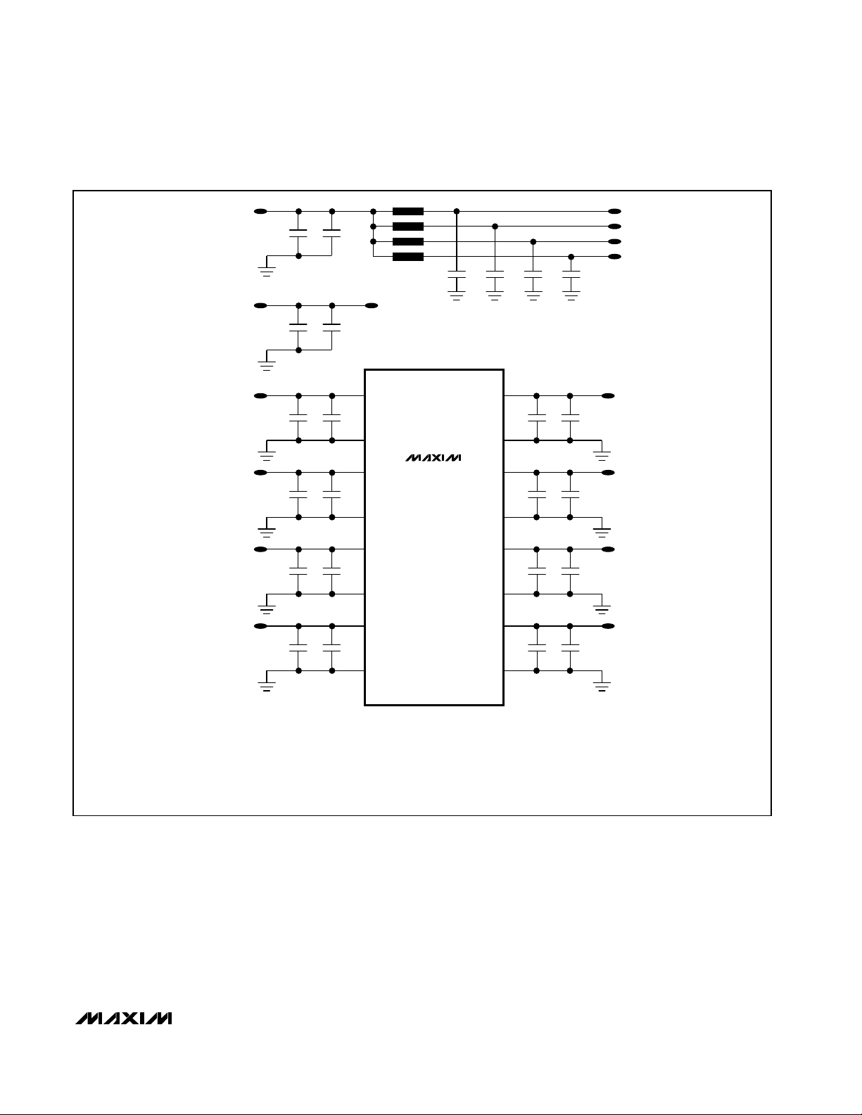
Grounding, Bypassing,
and Board Layout
Grounding and power supply decoupling strongly influence the MAX105’s performance. At 800MHz clock frequency and 6-bit resolution, unwanted digital crosstalk
may couple through the input, reference, power supply,
ground connections, and adversely influence the
dynamic performance of the ADC. In addition, the I&Q
inputs may crosstalk through poorly designed decoupling circuits. Therefore, closely follow the grounding
and power-supply decoupling guidelines in Figure 9.
Maxim strongly recommends using a multilayer printed
circuit board (PC board) with separate ground and
power supply planes. Since the MAX105 has separate
analog and digital ground connections (AGND, AGNDI,
AGNDQ, AGNDR, OGNDI, and OGNDQ, respectively).
The PC board should feature separate sections designated to analog (AGND) and digital (OGND), connected at only one point. Digital signals should run above
the digital ground plane and analog signals should run
above the analog ground plane. Keep digital signals far
away from the sensitive analog inputs, reference inputs,
and clock inputs. High-speed signals, including clocks,
analog inputs, and digital outputs, should be routed on
50Ω microstrip lines, such as those employed on the
MAX105EV kit.
The MAX105 has separate analog and digital powersupply inputs:
• AV
CC
= +5V ±5%: Power supply for the analog
input section of the clock circuit.
• AV
CC
I = +5V ±5%: Power supply for the I-channel
common-mode buffer, pre-amp and quantizer.
• AV
CC
Q = +5V ±5%: Power supply for the Q-chan-
nel common-mode buffer, pre-amp and quantizer.
• AV
CC
R = +5V ±5%: Power supply for the on-chip
bandgap reference.
• OV
CC
I = +3.3V ±10%: Power supply for the I-chan-
nel output drivers and DREADY circuitry.
• OV
CC
Q = +3.3V ±10%: Power supply for the
Q-channel output drivers and DOR circuitry.
All supplies should be decoupled with large tantalum or
electrolytic capacitors at the point they enter the PC
board. For best performance, bypass all power sup-
Dual, 6-Bit, 800Msps ADC with On-Chip,
Wideband Input Amplifier
16 ______________________________________________________________________________________
Figure 8. Typical I/Q Application
DREADY+/DREADY-
FROM PREVIOUS STAGE
MAX2108
QUADRATURE
DEMODULATOR
90°
NYQUIST
FILTER
LO
2kΩ
PRE-AMP
CM BUFFER
I ADC
REF
1:2
REFERENCE
DOR
PRIMARY
DATA PORT
P0I-P5I
AUXILIARY
DATA PORT
A0I-A5I
AV
CC
10kΩ
D
S
P
10kΩ
CM BUFFER
PRE-AMP
NYQUIST
FILTER
2kΩ
REF
Q ADC
PRIMARY
DATA PORT
P0Q-P5Q
AUXILIARY
DATA PORT
A0Q-A5Q
DOR+/DOR-
Page 17
plies to the appropriate ground with a 10µF tantalum
capacitor, to filter power supply noise, in parallel with a
0.1µF capacitor. A combination of 0.01µF in parallel
with high quality 47pF ceramic chip capacitor located
very close to the MAX105 device filters high frequency
noise. A properly designed PC board (see MAX105EV
Kit data sheet) allows the user to connect all analog
supplies and all digital supplies together thereby
requiring only two separate power sources. Decoupling
AVCC, AVCCI, AVCCQ and AVCCR with ferrite-bead
suppressors prevents further crosstalk between the
individual analog supply pins
Thermal Management
The MAX105 is designed for a thermally enhanced 80pin TQFP package, providing greater design flexibility,
increased thermal efficiency and a low thermal junction-case (θjc) resistance of ≈1.26°C/W. In this pack-
MAX105
Dual, 6-Bit, 800Msps ADC with On-Chip,
Wideband Input Amplifier
______________________________________________________________________________________ 17
Figure 9. MAX105 Decoupling, Bypassing and Grounding
PC BOARD AV
PC BOARD AGND FERRITE-BEAD
PC BOARD OV
PC BOARD OGND
AGNDR
AV
AGNDI
AVCCQ
AGNDQ
AV
AGND
CC
10µF
CC
10µF
10nF
I
CC
10nF
10nF
CC
10nF
10nF
10nF
47pF
47pF
47pF
47pF
SUPPRESSORS
OV
CC
RAVCCR
AV
CC
AGNDR
AV
I
CC
AGNDI
AV
Q
CC
AGNDQ
AV
CC
AGND
I, OVCCQ
MAX105
OV
OGNDI
OVCCI
OGNDI
OV
CC
OGNDQ
OVCCQ
OGNDQ
4 x 10nF
10nF
10nF
10nF
10nF
OV
CC
OGNDI
OV
CC
OGNDI
OV
CC
OGNDQ
OVCCQ
OGNDQ
I
I
Q
I
CC
47pF
47pF
Q
47pF
47pF
NOTE:
LOCATE ALL 47pF AND 10nF CAPACITORS, WHICH DECOUPLE AV
AS POSSIBLE TO THE CHIP. IT IS ALSO RECOMMENDED TO CONNECT ALL ANALOG GROUND CONNECTIONS TO A COMMON ANALOG
GROUND PLANE AND ALL DIGITAL GROUND CONNECTIONS TO ONE COMMON DIGITAL GROUND PLANE ON THE PC BOARD. A SIMILAR
TECHNIQUE CAN BE USED FOR ALL ANALOG AND DIGITAL POWER SUPPLIES.
AV
= AVCCI = AVCCQ = AVCCR = +5V±5%
CC
OVCCI = OVCCQ = +3.3V±10%
I, AVCCQ, AVCCR, OVCCI, AND OVCCQ AS CLOSE
CC
Page 18
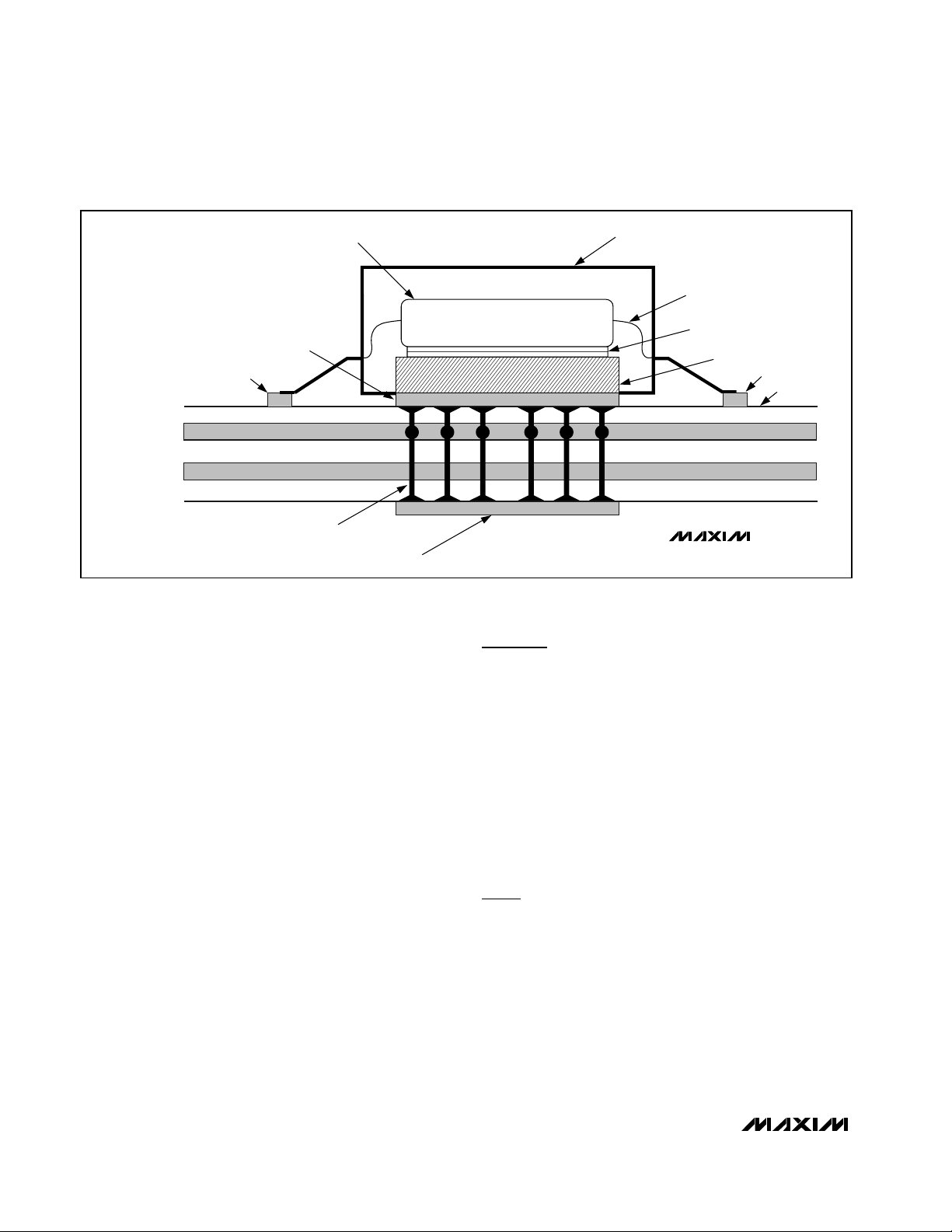
MAX105
Dual, 6-Bit, 800Msps ADC with On-Chip,
Wideband Input Amplifier
18 ______________________________________________________________________________________
age, the data converter die is attached to an exposed
pad (EP) leadframe using a thermally conductive
epoxy. The package is molded in a way, that this leadframe is exposed at the surface, facing the printed circuit board (PC board) side of the package (Figure 10).
This allows the package to be attached to the PC board
with standard infrared (IR) flow soldering techniques. A
specially created land pattern on the PC board, matching the size of the EP (7.5mm x 7.5mm) does not only
guarantee proper attachment of the chip, but can also
be used for heat-sinking purposes. Designing thermal
vias* into the land area and implementing large ground
planes in the PC board design, further enhance the
thermal conductivity between board and package. To
remove heat from an 80-pin TQFP package efficiently,
an array of 6 x 6 vias (≤ 0.3mm diameter per via hole
and 1.2mm pitch between via holes) is required.
Note: Efficient thermal management for the MAX105 is
strongly depending on PC board and circuit design,
component placement, and installation. Therefore,
exact performance figures cannot be provided.
However, the MAX105EV kit exhibits a typical θja of
18°C/W. For more information on proper design techniques and recommendations to enhance the thermal
performance of parts such as the MAX105, please refer
to Amkor Technology’s website at www.amkor.com.
Static Parameter Definitions
Integral Nonlinearity (INL)
Integral nonlinearity is the deviation of the values on an
actual transfer function from a straight line. This straight
line is drawn between the endpoints of the transfer
function, once offset and gain errors have been nullified. The static linearity parameters for the MAX105 are
measured using the sine-histogram method.
Differential Nonlinearity (DNL)
Differential nonlinearity is the difference between an
actual step-width and the ideal value of 1LSB. A DNL
error specification of greater than -1LSB guarantees no
missing codes and a monotonic transfer function.
Dynamic Parameter Definitions
Aperture Jitter and Delay
Aperture uncertainties affect the dynamic performance
of high-speed converters. Aperture jitter, in particular,
directly influences SNR and limits the maximum slew
rate (dV/dt) that can be digitized without significant
error. Aperture jitter limits the SNR performance of the
ADC, according to the following relationship:
SNRdB= 20 x log10[1 / (2 x π x fINx t
AJ[RMS]
)],
where f
IN
represents the analog input frequency and
tAJis the RMS aperture jitter. The MAX105’s innovative
Figure 10. MAX105 Exposed Pad Package Cross-Section
*Connects the land pattern to internal or external copper planes.
DIE
THERMAL LAND
COPPER PLANE, 1oz.
COPPER TRACE, 1oz.
TOP LAYER
GROUND PLANE
AGND, DGND
POWER PLANE
GROUND PLANE (AGND)
6 x 6 ARRAY OF THERMAL VIAS
THERMAL LAND
COPPER PLANE, 1oz.
80-PIN TQFP PACKAGE
WITH EXPOSED PAD
BONDING WIRE
EXPOXY
EXPOSED PAD
MAX105
COPPER
TRACE, 1oz.
PC BOARD
Page 19

clock design limits aperture jitter to typically 1.5ps
RMS
.
Figure 11 depicts the aperture jitter (tAJ), which is the
sample-to-sample variation in the aperture delay.
Aperture delay (tAD) is the time defined between the
rising edge of the sampling clock and the instant when
an actual sample is taken (Figure 11).
Signal-to-Noise Ratio (SNR)
For a waveform perfectly reconstructed from digital
samples, the theoretical maximum SNR is the ratio of
the full-scale analog input (RMS value) to the RMS
quantization error (residual error). The ideal, theoretical
minimum analog-to-digital noise is caused by quantization error only and results directly from the ADC’s resolution (N-Bits):
SNR
MAX[dB]
= 6.02dBx N + 1.76
dB
In reality, there are other noise sources besides quantization noise: thermal noise, reference noise, clock jitter
(see Aperture Uncertainties). SNR is computed by tak-
ing the ratio of the RMS signal to the RMS noise, which
includes all spectral components minus the fundamental, the first four harmonics, and the DC offset.
Signal-to-Noise Plus Distortion (SINAD)
SINAD is computed by taking the ratio of the RMS signal to all spectral components minus the fundamental
and the DC offset.
Effective Number of Bits (ENOB)
ENOB specifies the dynamic performance of an ADC at
a specific input frequency, amplitude, and sampling
rate relative to an ideal ADC’s quantization noise. For a
full-scale input ENOB is computed from:
ENOB = (SINAD - 1.76
dB
) / 6.02
dB
Total Harmonic Distortion (THD)
THD is typically the ratio of the RMS sum of the first four
harmonics of the input signal to the fundamental itself.
This is expressed as:
where V1 is the fundamental amplitude, and V2through
V5are the amplitudes of the 2nd- through 5th-order harmonics.
Spurious-Free Dynamic Range (SFDR)
SFDR is the ratio expressed in decibels of the RMS
amplitude of the fundamental to the RMS value of the
next largest spurious component, excluding DC offset.
Two-Tone Intermodulation
Distortion (IMD)
The two-tone IMD is the ratio expressed in decibels of
either input tone to the worst 3rd-order (or higher) intermodulation products. The individual input tone levels
are at -7dB full-scale and their envelope peaks at -1dB
full-scale.
Chip Information
TRANSISTOR COUNT: 12,286
MAX105
Dual, 6-Bit, 800Msps ADC with On-Chip,
Wideband Input Amplifier
______________________________________________________________________________________ 19
Figure 11. Aperture Timing
CLK-
CLK+
ANALOG
INPUT
t
AD
SAMPLING
INSTANT
t
AW
tAW: APERTURE WIDTH
: APERTURE JITTER
t
AJ
t
AJ
: APERTURE DELAY
t
AD
MAX105
THD x V V V V V=+++20
log ( ) / )
22324
25212
Page 20

MAX105
Dual, 6-Bit, 800Msps ADC with On-Chip,
Wideband Input Amplifier
20 ______________________________________________________________________________________
Pin Configuration
T.P.
REF
AV
CC
AGNDR
AGNDI
INI-
INI+
AGNDI
AV
CC
CLK+
CLK-
AV
CC
AGNDQ
INQ+
INQ-
AGNDQ
AGND
AGND
AV
T.P.
CC
I
A5I+
A5I-
P5I+
P5I-
A4I+
A4I-
P4I+
77
80
1
2
R
3
4
5
6
7
8
I
9
10
11
Q
12
13
14
15
16
17
18
19
20
78
79
76
74
75
P4I-
73
CC
OV
72
OGNDI
71
MAX105
A3I+
70
A3I-
69
P3I+
68
P3I-
67
OGNDI
66
I
CC
OV
A2I+
65
64
A2I-
63
P2I+
62
P2I-
61
60
59
58
57
56
55
54
53
52
51
50
49
48
47
46
45
44
43
42
41
A1I+
A1I-
P1I+
P1I-
A0I+
A0I-
P01+
P01-
DREADY+
DREADY-
DOR-
DOR+
P0Q-
P0Q+
A0Q-
A0Q+
P1Q-
P1Q+
A1Q-
A1Q+
21
A5Q+
22
A5Q-
23
P5Q+
24
P5Q-
25
A4Q+
26
A4Q-
P4Q+
28
P4Q-
29
30
31
32
Q
CC
OV
OGNDQ
A3Q+
A3Q-
33
P3Q+
34
P3Q-
36
35
Q
CC
OV
OGNDQ
37
A2Q+
38
A2Q-
39
P2Q+
40
P2Q-
27
Page 21

MAX105
Dual, 6-Bit, 800Msps ADC with On-Chip,
Wideband Input Amplifier
Maxim cannot assume responsibility for use of any circuitry other than circuitry entirely embodied in a Maxim product. No circuit patent licenses are
implied. Maxim reserves the right to change the circuitry and specifications without notice at any time.
Maxim Integrated Products, 120 San Gabriel Drive, Sunnyvale, CA 94086 408-737-7600 ____________________ 21
© 2001 Maxim Integrated Products Printed USA is a registered trademark of Maxim Integrated Products.
Package Information
 Loading...