

Page 1
_______________General Description
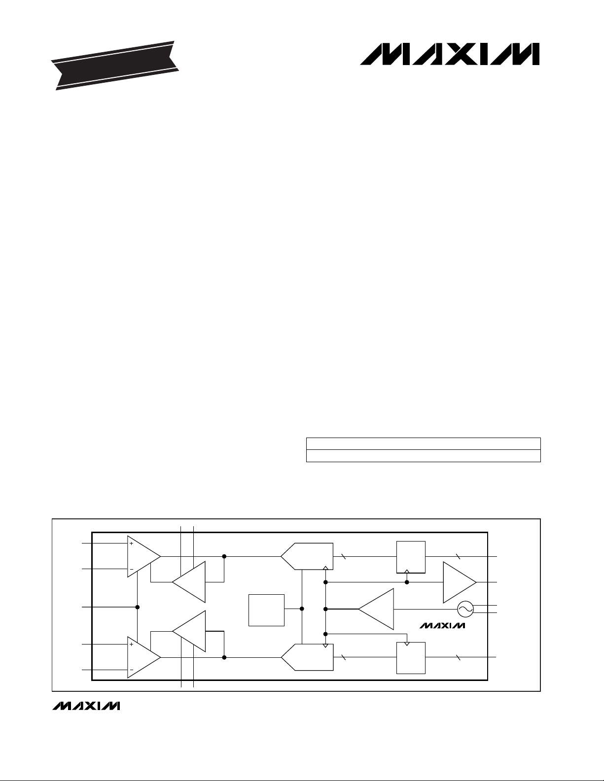
The MAX1002 is a dual, 6-bit analog-to-digital converter
(ADC) that combines high-speed, low-power operation
with a user-selectable input range, an internal reference, and a clock oscillator. The dual, parallel ADCs
are designed to convert in-phase (I) and quadrature
(Q) analog signals into two 6-bit offset-binary-coded
digital outputs at sampling rates up to 60Msps while
achieving typical integral nonlinearity (INL) and differential nonlinearity (DNL) of ±1/4LSB. The ability to
interface directly with baseband I and Q signals makes
the MAX1002 ideal for use in direct-broadcast satellite,
VSAT, and QAM16 demodulation applications.
The MAX1002 input amplifiers feature true differential
inputs, a 55MHz -0.5dB analog bandwidth, and userprogrammable input full-scale ranges of 125mVp-p,
250mVp-p, or 500mVp-p. With an AC-coupled input
signal, matching performance between input channels
is typically 0.1dB gain, 1/4LSB offset, and 0.5° phase.
Dynamic performance is 5.85 effective number of bits
(ENOB) with a 20MHz analog input signal, or 5.78
ENOB with a 50MHz input signal.
The MAX1002 operates with a single +5V power supply
and provides TTL-compatible digital outputs. The device
is available in the commercial temperature range (0°C to
+70°C) and comes in a 36-pin SSOP package.
________________________Applications
Direct Broadcast Satellite (DBS) Receivers
VSAT Receivers
Wide Local Area Networks (WLAN)
Cable Television Set-Top Boxes
____________________________Features
♦ ±1/4LSB INL and DNL, Typical
♦ 1/4LSB (typ) Channel-to-Channel Offset Matching
♦ 0.1dB Gain and 0.5° Phase Matching, Typical
♦ Internal Bandgap Voltage Reference
♦ Two Matched 6-Bit, 60Msps ADCs
♦ Excellent Dynamic Performance:
5.85 ENOB with 20MHz Analog Input
5.7 ENOB with 50MHz Analog Input
♦ Internal Oscillator with Overdrive Capability
♦ 55MHz (-0.5dB) Bandwidth Input Amplifiers
with True Differential Inputs
♦ User-Selectable Input Full-Scale Range
(125mVp-p, 250mVp-p, or 500mVp-p)
♦ Single-Ended or Differential Input Drive
♦ +5V Single Supply
♦ TTL Outputs
♦ 90Msps Upgrade with +3.3V CMOS-Compatible
Output Available (MAX1003)
MAX1002
Low-Power, 60Msps, Dual, 6-Bit ADC
________________________________________________________________
Maxim Integrated Products
1
MAX1002
DATA
BUFFER
Q
CLOCK
DRIVER
D0I–D5I
DCLK
TNK+
TNK-
DQ0–DQ5
INPUT
AMP
I
IIN+
IIN-
GAIN
QIN+
QIN-
CLOCK
OUT
DATA
BUFFER
I
6
ADC
I
ADC
Q
VREF
VREF
BANDGAP
REFERENCE
OFFSET
CORREC-
TION Q
OFFSET
CORREC-
TION I
INPUT
AMP
Q
QOCC+ QOCC-
IOCC+ IOCC-
6
6
6
_________________________________________________________Functional Diagram
19-1270; Rev 0; 7/97
PART
MAX1002CAX 0°C to +70°C
TEMP. RANGE PIN-PACKAGE
36 SSOP
EVALUATION KIT
AVAILABLE
______________Ordering Information
Pin Configuration appears at end of data sheet.
For free samples & the latest literature: http://www.maxim-ic.com, or phone 1-800-998-8800
For small orders, phone 408-737-7600 ext. 3468.
Page 2
MAX1002
Low-Power, 60Msps, Dual, 6-Bit ADC
2 _______________________________________________________________________________________
ABSOLUTE MAXIMUM RATINGS
DC ELECTRICAL CHARACTERISTICS
(VCC, V
CCO
= +5V ±5%; TA= T
MIN
to T
MAX
; unless otherwise noted.)
Stresses beyond those listed under “Absolute Maximum Ratings” may cause permanent damage to the device. These are stress ratings only, and functional
operation of the device at these or any other conditions beyond those indicated in the operational sections of the specifications is not implied. Exposure to
absolute maximum rating conditions for extended periods may affect device reliability.
VCCto GND .........................................................-0.3V to +6.5V
V
CCO
to OGND.........................................................-0.3V, +6.5V
GND to OGND .........................................................-0.3V, +0.3V
Digital and Clock Output Pins to OGND ........-0.3V, V
CCO
(<10sec)
All Other Pins to GND..................................................-0.3V, V
CC
Continuous Power Dissipation (TA= +70°C)
SSOP (derate 45mW/°C above +70°C) ......................941mW
Operating Temperature Range...............................0°C to +70°C
Storage Temperature Range.............................-65°C to +150°C
Lead Temperature (soldering, <10sec)...........................+300°C
CONDITIONS
LSB-0.5 ±0.25 0.5INLIntegral Nonlinearity
Bits6RESResolution
UNITSMIN TYP MAXSYMBOLPARAMETER
GAIN = open (mid gain)
GAIN = VCC(high gain)
No missing codes over temperature
237.5 250 262.5V
FSM
118.75 125 131.25V
FSH
LSB-0.5 ±0.25 0.5DNLDifferential Nonlinearity
Other analog input driven with external source
(Note 2)
Guaranteed by design
V1.75 2.75V
CM
GAIN = GND (low gain)
Common-Mode Voltage Range
pF3 5C
IN
Input Capacitance
kΩ13 20 29R
IN
Input Resistance
V2.25 2.35 2.45V
AOC
Input Open-Circuit Voltage
mVp-p
475 500 525V
FSL
Full-Scale Input Range
Other oscillator input tied to VCC+ 0.3V
I
SOURCE
= 50µA V2.4V
OH
Digital Outputs Logic-High
Voltage
kΩ4.8 8 12.1R
OSC
Oscillator Input Resistance
I
SINK
= 400µA V0.5V
OL
Digital Outputs Logic-Low
Voltage
VCC= 4.75V to 5.25V (Note 3)
20MHz, FS I & Q analog inputs,
C
LOAD
= 15pF (Note 4)
mW380PDPower Dissipation
mA24I
CCO
Digital Outputs Supply Current
dB-75 -40PSRRPower-Supply Rejection Ratio
mA63 104I
CC
Supply Current
DC ACCURACY (Note 1)
INVERTING AND NONINVERTING ANALOG INPUTS
OSCILLATOR INPUTS
DIGITAL OUTPUTS (DI0–DI5, DQ0–DQ5)
POWER SUPPLY
Page 3
MAX1002
Low-Power, 60Msps, Dual, 6-Bit ADC
_______________________________________________________________________________________ 3
AC ELECTRICAL CHARACTERISTICS
(V
CC,VCCO
= +5V ±5%; TA= +25°C; unless otherwise noted.)
Note 1: Best straight-line linearity method.
Note 2: A typical application will AC couple the analog input to the DC bias level present at the analog inputs (typically 2.35V).
However, it is also possible to DC couple the analog input (using differential or single-ended drive) within this commonmode input range (Figures 4, 5).
Note 3: PSSR is defined as the change in the mid-gain, full-scale range as a function of the variation in V
CC
supply voltage
(expressed in decibels).
Note 4: The current in the V
CCO
supply is a strong function of the capacitive loading on the digital outputs. To minimize supply
transients and achieve the best dynamic performance, reduce the capacitive loading effects by keeping line lengths on the
digital outputs to a minimum.
Note 5: Offset-correction compensation enabled, 0.22µF at Q and I compensation inputs (Figures 2, 3).
Note 6: t
PD
and t
SKEW
are measured from the 1.4V level of the output clock, to the 1.4V level of either the rising or falling edge of a
data bit. t
DCLK
is measured from the 50% level of the clock overdrive signal on TNK+ to the 1.4V level of D
CLK
. The capac-
itive load on the outputs is 15pF.
Gain = GND, open, V
CC
GAIN = open (mid gain),
VIN= 50MHz, -1dB below FS
GAIN = open (mid gain)
5.7
ENOB
M
5.6 5.85
Effective Number of Bits
Gain = open (mid gain)
Gain = VCC(low gain)
Q channel
I channel
dB
CONDITIONS
MHz55BWAnalog Input -0.5dB Bandwidth
Msps60f
MAX
Maximum Sample Rate
-55XTLK
Gain = VCC(high gain)
Crosstalk Between ADCs
LSB
-0.5 0.5
OFFInput Offset (Note 5)
-0.5 0.5
dB35.4 37SINAD
Signal-to-Noise and Distortion
Ratio
Bits
5.85ENOB
L
5.8ENOB
H
(Note 5)
dB-0.2 ±0.1 0.2AM
Amplitude Match Between
ADCs
LSB-0.5 ±0.25 0.5OMM2Offset Mismatch Between ADCs
(Note 6)
(Note 6)
ns3.6t
SKEW
Data Valid Skew
ns7.1t
PD
DCLK to Data-Propagation
Delay
degrees-2 ±0.5 2PM
UNITSMIN TYP MAXSYMBOLPARAMETER
Phase Match Between ADCs
TNK+ to DCLK (Note 6) ns5.3t
DCLK
Input to DCLK Delay
ns5.5t
AP
Aperture Delay
clock
cycle
1PDPipeline Delay
DYNAMIC PERFORMANCE (GAIN = open; external 60MHz clock (Figure 7); V
INI
, V
INIQ
= 20MHz sine; amplitude -1dB below FS;
unless otherwise noted.)
TIMING CHARACTERISTICS (data outputs: RL= 1MΩ, CL= 15pF, Figure 8)
Page 4
MAX1002
Low-Power, 60Msps, Dual, 6-Bit ADC
4 _______________________________________________________________________________________
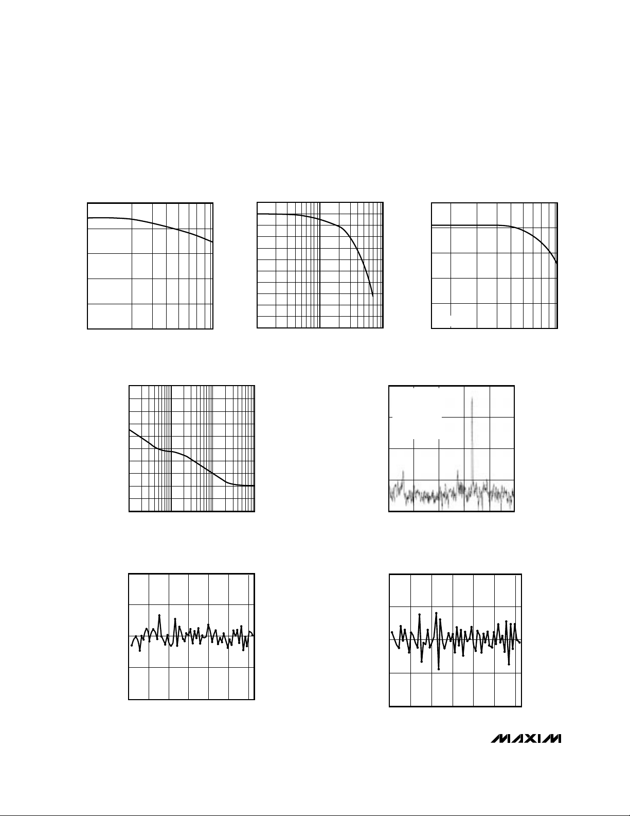
__________________________________________Typical Operating Characteristics
(V
CC, VCCO
= +5V ±5%; MAX1002/MAX1003 evaluation kit; TA= +25°C; unless otherwise noted.)
6.0
5.0
10
100
EFFECTIVE NUMBER OF BITS
vs. ANALOG INPUT FREQUENCY
5.2
MAX1002-01
ANALOG INPUT FREQUENCY (MHz)
ENOB (bits)
5.4
5.6
5.8
f
CLK
= 60Msps
-1.0
1 10 100
ANALOG INPUT BANDWIDTH
-0.8
MAX1002-02
ANALOG INPUT FREQUENCY (MHz)
MAGNITUDE (dB)
-0.6
-0.2
-0.4
0
5.5
10 100
EFFECTIVE NUMBER OF BITS
vs. SAMPLING FREQUENCY
5.6
MAX1002-03
SAMPLING FREQUENCY (MHz)
ENOB
5.7
5.9
5.8
6.0
fIN = 20MHz
-50
-70
-150
1k 100k 1M
OPEN-LOOP PHASE NOISE
vs. FREQUENCY
-130
-90
-110
MAX1002-TOC4
FREQUENCY (Hz)
PHASE NOISE (dBc)
10k
0.50
-0.50
DIFFERENTIAL NONLINEARITY
vs. CODE
-0.25
0.25
MAX1002-06
CODE
DNL (LSB)
0
0 6410 20 30 40 50 60
0.50
-0.50
DIFFERENTIAL NONLINEARITY
vs. CODE
-0.25
0.25
MAX1002-07
DNL (LSB)
0
0 6410 20 30 40 50 60
-80
-40
-60
-20
0
0 6 12 18 24 30
FFT PLOT
MAX1002-05
FREQUENCY (MHz)
fIN = 19.930MHz
f
CLK
= 60.000MHz
1024 POINTS
AC COUPLED
SINGLE ENDED
AVERAGED
Page 5

_______________Detailed Description
Converter Operation
The MAX1002 contains two 6-bit analog-to-digital converters (ADCs), a buffered voltage reference, and oscillator circuitry. The ADCs use a flash-conversion
technique to convert an analog input signal into a 6-bit
parallel digital output code. The MAX1002’s unique
design includes 63 fully differential comparators and a
proprietary encoding scheme that ensures no more
than 1LSB dynamic encoding error. The control logic
interfaces easily to most digital signal processors
(DSPs) and microprocessors (µPs) with +5V CMOScompatible logic interfaces. Figure 1 shows the
MAX1002 in a typical application.
Programmable Input Amplifiers
The MAX1002 has in-phase (I) and quadrature (Q) programmable-gain input amplifiers with a 55MHz
-0.5dB bandwidth and true differential inputs. To maximize performance in high-speed systems, each amplifier
has less than 5pF of input capacitance. The input amplifier gain is programmed via the GAIN pin to provide
three possible input full-scale ranges (FSR) (Table 1).
MAX1002
Low-Power, 60Msps, Dual, 6-Bit ADC
_______________________________________________________________________________________ 5
______________________________________________________________Pin Description
PIN
Gain-Select Input. Sets input full-scale range: 125/250/500mVp-p (Table 1).GAIN1
FUNCTIONNAME
Positive I-Channel Offset-Correction Compensation. Connect 0.22µF capacitor
for AC-coupled inputs (Figures 2, 3). Ground for DC-coupled inputs (Figures 4, 5).
IOCC+2
I-Channel Noninverting Analog InputIIN+4
Negative I-Channel Offset-Correction Compensation. Connect 0.22µF capacitor
for AC-coupled inputs (Figures 2, 3). Ground for DC-coupled inputs (Figures 4, 5).
IOCC-3
+5V ±5% Supply. Bypass with 0.01µF capacitor to GND (Pin 7).V
CC
6
+5V ±5% Supply. Bypass with 0.01µF capacitor to GND (Pin 11).V
CC
8
Analog GroundGND
7, 11, 12,
18, 19
I-Channel Inverting Analog InputIIN-5
Negative Oscillator/Clock InputTNK-10
Q-Channel Inverting Analog InputQIN-14
+5V ±5% Supply. Bypass with 0.01µF capacitor to GND (Pin 12).V
CC
13
Negative Q-Channel Offset-Correction Compensation. Connect 0.22µF capacitor
for AC-coupled inputs (Figures 2, 3). Ground for DC-coupled inputs (Figures 4, 5).
QOCC-16
Q-Channel Digital Outputs 0–5. DQ5 is the most significant bit (MSB).DQ5–DQ020–25
Positive Q-Channel Offset-Correction Compensation. Connect 0.22µF capacitor
for AC-coupled inputs (Figures 2, 3). Ground for DC-coupled inputs (Figures 4, 5).
QOCC+17
Q-Channel Noninverting Analog InputQIN+15
Positive Oscillator/Clock InputTNK+9
Digital Output GroundOGND27
I-Channel Digital Outputs 0–5. DI5 is the most significant bit (MSB).DI0–DI530–35
Digital Clock Output. Frames the output data.DCLK29
+5V ±5% Digital Supply. Bypass each with 47pF to OGND (Pin 27).V
CCO
26, 28
+5V ±5% Supply. Bypass with 0.01µF to GND (Pin 19).V
CC
36
250Open
125V
CC
GAIN
500GND
INPUT FULL-SCALE RANGE
(mVp-p)
Table 1. Input Amplifier Programming
Page 6

MAX1002
Figures 2 and 3 show single-ended and differential ACcoupled input circuits. Each of the amplifier inputs is
internally biased to a 2.35V reference through a 20kΩ
resistor, eliminating external DC bias circuits. A series
0.1µF capacitor is required at each amplifier input for
AC-coupled signals.
When operating with AC-coupled inputs, the input
amplifiers’ DC offset voltage is nulled to within ±1/2LSB
by an on-chip offset-correction amplifier. An external
compensation capacitor is required to set the dominant
pole of the offset-correction amplifier’s frequency
response (Figures 2 and 3). The compensation capacitor determines the low-frequency corner of the analog
input response according to the following formula:
fc= 1 / (0.1 x C)
where C is the value of the compensation capacitor in
µF, and fc is the corner frequency in Hz.
Low-Power, 60Msps, Dual, 6-Bit ADC
6 _______________________________________________________________________________________
0
DIV
60Msps
DATA
BUFFER
TANK
MODCTL CAR
SYNTHESIZER
FIN
IIN
AGC
CLK IN
DSP
QIN
DAC OR
ADC CLOCK
6 BITS
TANK
LO
TSA5055 or
EQUIVALENT
90
OFFSET CORRECTION
OFFI
OFFI
OFFQ
OFFQ
PSOUT MOD GND (x8)
AGC
IOUT
QOUT
V
CC
(x7)
FROM TANK VOLTAGE
VARACTOR-TUNED
PRESELECTION FILTER
EXTERNAL
VCO
OR
OR
F-CONNECTOR
FOR 2ND SET-TOP BOX
KU BAND
75Ω CABLE
950MHz TO 2150MHz
F-CONNECTOR
INPUT
MAX2102
MAX1002
DATA
BUFFER
6 BITS
LO
RFIN
RFIN
LNB
Figure 1. Commercial Satellite Receiver System
Page 7

Figures 4 and 5 show single-ended and differential DCcoupled input circuits for applications where a DC component of the input signal is present. The amplifiers’
input common-mode voltage range extends from 1.75V
to 2.75V. To prevent attenuation of the input signal’s DC
component when operating in this mode, disable the offset-correction amplifier by grounding the _OCC+ and
_OCC- pins for the I and Q blocks (Figures 4 and 5).
ADCs
The I and Q ADC blocks receive the analog signals
from the respective I and Q input amplifiers. The ADCs
use flash conversion with 63 fully differential comparators to digitize the analog input signal into a 6-bit output
in offset binary format.
MAX1002
Low-Power, 60Msps, Dual, 6-Bit ADC
_______________________________________________________________________________________ 7
Figure 2. Single-Ended AC-Coupled Input
Figure 3. Differential AC-Coupled Input
Figure 4. Single-Ended DC-Coupled Input
Figure 5. Differential DC-Coupled Input
MAX1002
INPUT
AMP
20k
2.35V INTERNAL REFERENCE
20k
_IN+
_OCC+ _OCC-
_IN-
0.1µF
0.22µF
V
SOURCE
0.1µF
OFFSET
CORREC-
TION
(ONE CHANNEL SHOWN)
0.22µF
_OCC+ _OCC-
OFFSET
CORREC-
TION
0.1µF
_IN+
V
SOURCE
0.1µF
_IN-
20k
INPUT
AMP
20k
2.35V INTERNAL REFERENCE
MAX1002
_IIN+
V
SOURCE
V
CM
1.75V TO 2.75V
(ONE CHANNEL SHOWN)
_IIN-
20k
OFFSET-CORRECTION DISABLED
_IOCC+ _IOCC-
INPUT
AMP
20k
2.35V INTERNAL REFERENCE
OFFSET
CORREC-
TION
MAX1002
(ONE CHANNEL SHOWN)
_IIN+
20k
INPUT
AMP
V
SOURCE
DIFFERENTIAL SOURCE
WITH 1.75V TO 2.75V
COMMON-MODE
RANGE
(ONE CHANNEL SHOWN)
_IIN-
20k
OFFSET-CORRECTION DISABLED
_IOCC+ _IOCC-
OFFSET
CORREC-
TION
MAX1002
2.35V INTERNAL REFERENCE
Page 8

MAX1002
The MAX1002 features a proprietary encoding scheme
that ensures no more than 1LSB dynamic encoding
error. Dynamic encoding errors resulting from metastable states may occur when the analog input voltage,
at the time the sample is taken, falls close to the decision point for any one of the input comparators. The
resulting output code for typical converters can be
incorrect, including false full- or zero-scale outputs. The
MAX1002’s unique design reduces the magnitude of
this type of error to 1LSB.
Internal Voltage Reference
An internal buffered bandgap reference is included on
the MAX1002 to drive the ADC’s reference ladders. The
on-chip reference and buffer eliminate any external
(high-impedance) connections to the reference ladder,
minimizing the potential for noise coupling from external circuitry while ensuring that the voltage reference,
input amplifier, and reference ladder track well with
variations in temperature and power supplies.
Oscillator Circuit
The MAX1002 includes a differential oscillator, which is
controlled by an external parallel resonant (tank) network (Figure 6). As an alternative, the oscillator may be
overdriven with an external clock source (Figure 7).
Internal-Clock Operation (Tank)
If the tank circuit is used, the resonant inductor should
have a sufficiently high Q and a self-resonant frequency (SRF) of at least twice the intended oscillator frequency. Coilcraft's 1008HS-221, with a 700MHz SRF
and a Q of 45, works well for this application. Generate
different clock-frequency ranges by adjusting varactor
and tank elements.
An internal-clock-driver buffer is included to provide
sharp clock edges to the internal flash comparators.
The buffer ensures that the comparators are simultaneously clocked, maximizing the ADC’s effective number
of bits of performance.
External-Clock Operation
To accommodate designs that use an external clock,
the MAX1002’s internal oscillator can be overdriven by
an external clock source (Figure 7). The external clock
source should be a sinusoid to minimize clock-phase
noise and jitter, which can degrade the ADC’s effective
bits performance. AC couple the clock source (recommended voltage level is approximately 1Vp-p) to the
oscillator inputs (Figure 7).
Low-Power, 60Msps, Dual, 6-Bit ADC
8 _______________________________________________________________________________________
Figure 6. Tank-Resonator Oscillator
Figure 7. External-Clock-Drive Circuit
MAX1002
CL0CK
DRIVER
VARACTOR DIODE PAIR IS M/A-COM MA4ST079CK-287 (SOT23 PACKAGE).
INDUCTOR IS COILCRAFT 1008HS-221.
V
TUNE
= 0V TO 8V
f
OSC
= 55MHz TO 65MHz
TNK-
TNK+
V
TUNE
220nH
22pF
47pF
47pF
47k
47k
10k
50Ω
V
C
V
= 300mVp-p TO 1.25Vp-p
CLOCK
Z
0
= 50Ω
0.1µF
50Ω
0.1µF
50Ω
TNK+
CLOCK
DRIVER
TNK-
MAX1002
Page 9

Output Data Format
The conversion results are output on a dual 6-bit-wide
data bus. Data is latched into the ADC output latch following a pipeline delay of one clock cycle (Figure 8).
Output data is clocked out of the respective ADC’s dataoutput pins (D_0 through D_5) on the rising edge of the
clock output (DCLK), with a DCLK-to-data propagation
delay (tPD) of 7.1ns. The MAX1002 outputs are TTL compatible.
Transfer Function
Figure 9 shows the MAX1002’s nominal transfer function.
Output coding is offset binary with 1LSB = FSR / 63.
MAX1002
Low-Power, 60Msps, Dual, 6-Bit ADC
_______________________________________________________________________________________ 9
Figure 9. Ideal Transfer Function
111111
OUTPUT CODE
111110
111101
100001
100000
011111
011110
000011
000010
000001
000000
-FSR
2
0
1LSB
INPUT VOLTAGE
FSR
2
(_IN+ to _IN-)
Figure 8. MAX1002 Timing Diagram
DATA OUT
1.4V
DATA VALID N - 1 DATA VALID N
1.4V
50%
t
SKEW
t
DCLK
t
AP
t
PD
TNK+
(INPUT CLOCK)
DCLK
ANALOG
INPUT
N
N + 1
N + 2
Page 10

__________Applications Information
Layout, Grounding, and Bypassing
The MAX1002 is designed with separate analog and
digital power-supply and ground connections to isolate
high-current digital noise spikes from the more sensitive analog circuitry. The high-current digital output
ground (OGND) and analog ground (GND) should be
at the same DC level, connected at only one location
on the board. This provides best noise immunity and
improved conversion accuracy. Use of separate
ground planes is strongly recommended.
The entire board requires good DC bypassing for both
analog and digital supplies. Place the bypass capacitors close to where the power is routed onto the board,
i.e., close to the connector. 10µF electrolytic capacitors
with low ESR-ratings are recommended. For best effective bits performance, minimize capacitive loading at
the digital outputs. Keep the digital output traces as
short as possible.
The MAX1002 can operate with one +5V supply. For
optimum performance, separate +5V ±5% supplies and
bypassing are recommended. Bypass each of the V
CC
supply pins to its respective GND with highquality ceramic capacitors located as close to the
package as possible (Table 2). Consult the evaluation
kit for a suggested layout and bypassing scheme.
_____________Dynamic Performance
Signal-to-noise plus distortion (SINAD) is the ratio of the
fundamental input frequency’s RMS amplitude to all
other ADC output signals. The output spectrum is limited to frequencies above DC and below one-half the
ADC sample rate.
The theoretical minimum A/D noise is caused by quantization error, and results directly from the ADC’s resolution: SNR = (6.02N + 1.76)dB, where N is the number
of bits of resolution. Therefore, a perfect 6-bit ADC can
do no better than 38dB.
The FFT Plot (see
Typical Operating Characteristics
)
shows the result of sampling a pure 20MHz sinusoid at
a 60MHz clock rate. This FFT plot of the output shows
the output level in various spectral bands. The plot has
been averaged to reduce the quantization noise floor
and reveal the low-amplitude spurs. This emphasizes
the excellent spurious-free dynamic range of the
MAX1002.
The effective resolution (or ENOB) the ADC provides
can be measured by transposing the equation that converts resolution to SNR: N = (SINAD - 1.76) / 6.02 (see
Typical Operating Characteristics).
MAX1002
Low-Power, 60Msps, Dual, 6-Bit ADC
10 ______________________________________________________________________________________
Table 2. Bypassing
0.01µFOscillator/Clock
0.01µFConverter
SUPPLY
FUNCTION
0.01µFAnalog Inputs
CAPACITOR
VALUE
47pFDigital I Output
0.01µFBuffer
47pFDigital Q Output
27
19
11
27
12
BYPASS TO
GND/OGND
7
28
36
8
26
13
V
CC
/
V
CCO
6
Page 11

MAX1002
Low-Power, 60Msps, Dual, 6-Bit ADC
______________________________________________________________________________________ 11
__________________Pin Configuration ___________________Chip Information
36
35
34
33
32
31
30
29
28
27
26
25
24
23
1
2
3
4
5
6
7
8
9
10
11
12
13
14
V
CC
DI5
DI4
DI3
DI2
DI1
DQ2
DI0
DCLK
V
CCO
OGND
V
CCO
DQ0
DQ1
QIN-
V
CC
GND
GND
TNK-
TNK+
V
CC
GND
V
CC
IIN-
IIN+
IOCC-
IOCC+
GAIN
SSOP
TOP VIEW
MAX1002
22
21
20
19
15
16
17
18 GND
DQ3
DQ4
DQ5
GND
QOCC+
QOCC-
QIN+
TRANSISTOR COUNT: 6097
Page 12

MAX1002
Low-Power, 60Msps, Dual, 6-Bit ADC
________________________________________________________Package Information
SSOP2.EPS
Maxim cannot assume responsibility for use of any circuitry other than circuitry entirely embodied in a Maxim product. No circuit patent licenses are
implied. Maxim reserves the right to change the circuitry and specifications without notice at any time.
12
____________________Maxim Integrated Products, 120 San Gabriel Drive, Sunnyvale, CA 94086 408-737-7600
© 1997 Maxim Integrated Products Printed USA is a registered trademark of Maxim Integrated Products.
 Loading...