

Page 1
19-0282; Rev 0; 7/94
EVALUATION KIT
AVAILABLE
250Msps, 8-Bit ADC with Track/Hold
_______________General Description
The MAX100 ECL-compatible, 250Msps, 8-bit analog-todigital converter (ADC) allows accurate digitizing of analog signals from DC to 125MHz (Nyquist frequency).
Designed with Maxim’s proprietary advanced bipolar
processes, the MAX100 contains a high-performance
track/hold (T/H) amplifier and a quantizer in a single
ceramic strip-line package.
The innovative design of the internal T/H assures an
exceptionally wide input bandwidth of 1.2GHz and aperture delay uncertainty of less than 2ps, resulting in a high
6.8 effective bits performance. Special comparator output
design and decoding circuitry reduce out-of-sequence
code errors. The probability of erroneous codes occurring
due to metastable states is reduced to less than 1 error
per 1015clock cycles. Unlike other ADCs, which can
have errors that result in false full-scale or zero-scale outputs, the MAX100 keeps the magnitude to less than 1LSB.
The analog input is designed for either differential or singleended use with a ±270mV range. Sense pins for the reference input allow full-scale calibration of the input range or
facilitate ratiometric use. Midpoint tap for the reference
string is available for applications that need to modify the
output coding for a user-defined bilinear response. Use of
separate high-current and low-current ground pins provides better noise immunity and highest device accuracy.
Dual output data paths provide several data output modes
____________________________Features
♦ 250Msps Conversion Rate
♦ 6.8 Effective Bits at 125MHz
♦ Less than ±1/2LSB INL
♦ 50Ω Differential or Single-Ended Inputs
♦ ±270mV Input Signal Range
♦ Reference Sense Inputs
♦ Ratiometric Reference Inputs
♦ Configurable Dual-Output Data Paths
♦ Latched, ECL-Compatible Outputs
♦ Low Error Rate, Less than 10
-15
Metastable States
♦ Selectable On-Chip 8:16 Demultiplexer
♦ 84-Pin Ceramic Flat Pack
________________________Applications
High-Speed Digital Instrumentation
High-Speed Signal Processing
Medical Systems
Radar/Sonar
High-Energy Physics
Communications
______________Ordering Information
for easy interfacing. These modes can be configured as
either one or two identical latched ECL outputs. An 8:16
demultiplexer mode that reduces the output data rates to
one-half the clock rate is also available.
For applications that require faster data rates, refer to
PART
MAX100CFR* 0°C to +70°C
*Contact factory for 84-Pin Ceramic Flat Pack without heatsink.
TEMP. RANGE PIN-PACKAGE
84 Ceramic Flat Pack (with heatsink)
Maxim’s MAX101, which allows conversion rates up to
500Msps.
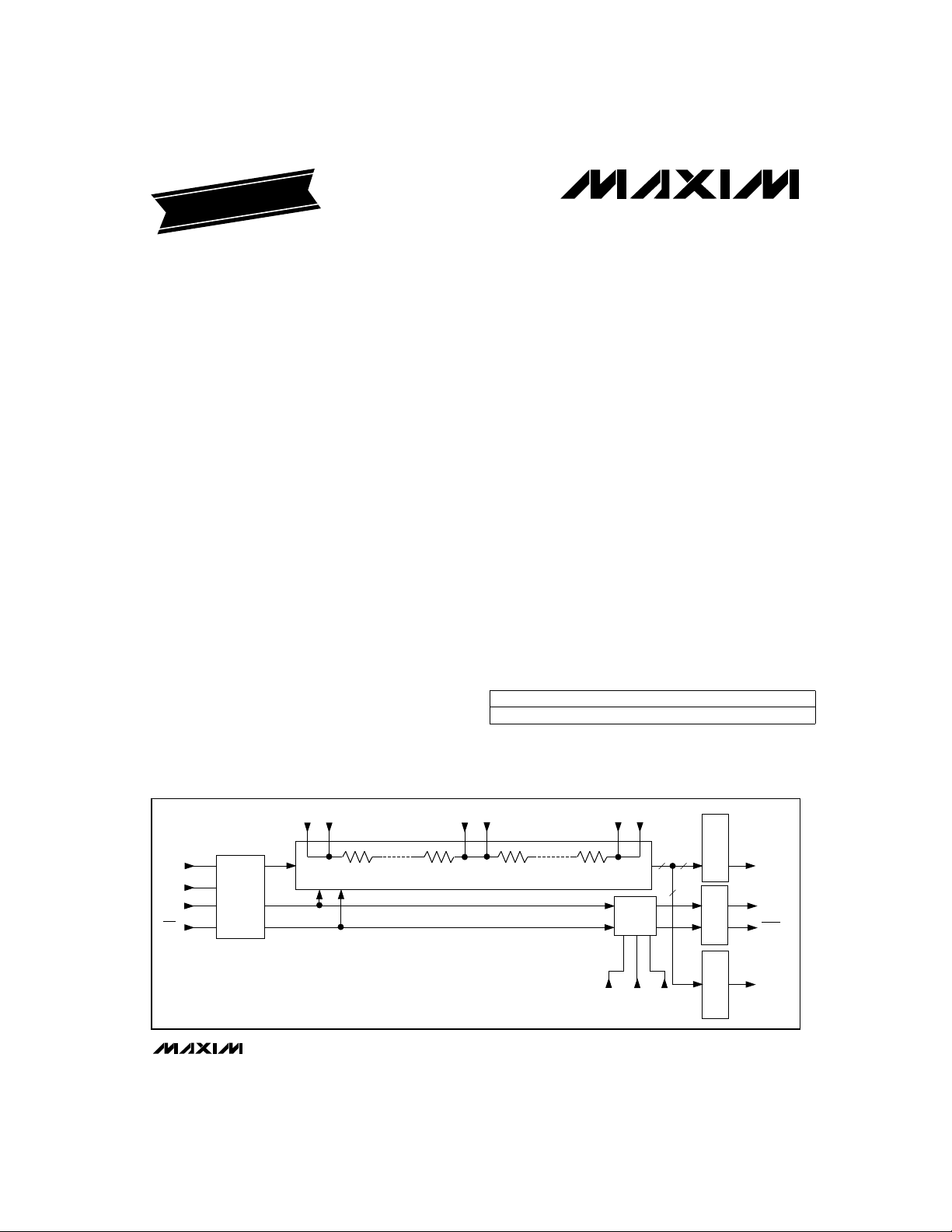
_________________________________________________________Functional Diagram
MAX100
VA
VA
CT
CTS
FLASH CONVERTER
AIN+
AIN-
CLK
CLK
VA
RTVARTS
TRACK/
HOLD
________________________________________________________________
Call toll free 1-800-998-8800 for free literature.
VA
VA
RB
RBS
8 8
8
MODE
CONTROL
DIVMOD
A=B
Maxim Integrated Products
L
A
T
C
H
E
AData
S
(A0–A7)
B
U
F
F
E
R
L
A
T
C
H
E
S
DCLK
DCLK
BData
(B0–B7)
1
Page 2
250Msps, 8-Bit ADC with Track/Hold
ABSOLUTE MAXIMUM RATINGS (Note 1)
Supply Voltages
.............................................................................0V to +7V
V
CC
...............................................................................-7V to 0V
V
EE
V
Analog Input Voltage.............................................................±2V
Digital Input Voltage.................................................-2.3V to +0V
Reference Voltage (VA
MAX100
............................................................................+12V
CC - VEE
).....................................-0.3V to +1.5V
RT
Reference Voltage (VA
Data Output Current ..........................................................-33mA
DCLK Output Current ........................................................-43mA
Operating Temperature Range...............................0°C to +70°C
Operating Junction Temperature (Note 2)............0°C to +125°C
Storage Temperature Range.............................-65°C to +150°C
Lead Temperature (soldering, 10sec).............................+250°C
Note 1: The digital control inputs are diode protected; however, permanent damage may occur on unconnected units under high-
energy electrostatic fields. Keep unused units in conductive foam or shunt the terminals together. Discharge the conductive foam to the destination socket before insertion.
Note 2: Typical thermal resistance, junction-to-case R
12°C/W, providing 200 lineal ft/min airflow with heatsink. See
Stresses beyond those listed under “Absolute Maximum Ratings” may cause permanent damage to the device. These are stress ratings only, and functional
operation of the device at these or any other conditions beyond those indicated in the operational sections of the specifications is not implied. Exposure to
absolute maximum rating conditions for extended periods may affect device reliability.
= 5°C/W and thermal resistance, junction to ambient (MAX100CA) R
θJC
Package Information.
ELECTRICAL CHARACTERISTICS
(VEE= -5.2V, VCC= +5V, RL= 50Ω to -2V, VART= 1.02V, VARB= -1.02V, T
otherwise noted.) (Note 3)
CONDITIONS
ACCURACY
AData, BData
INLIntegral Nonlinearity (Note 4)
AData, BData,
DNLDifferential Nonlinearity
no missing codes
DYNAMIC SPECIFICATIONS
f
= 250MHz,
CLK
ENOBEffective Bits
VIN= 95% full scale
(Note 5)
f
Maximum Conversion Rate
Analog Input Bandwidth
Aperture Width
Aperture Jitter
CLK
3dB
AW
AJ
= 50MHz, f
AIN
full scale (Note 6)
(Note 7)
Figure 5
Figure 5
= 250MHz, VIN= 95%
CLK
ANALOG INPUT
AIN+ to AIN-, Table 2,
Input Voltage Range
Input Offset Voltage
Least-Significant-Bit Size
Input Resistance
V
IN
TA= T
AIN+, AIN-, TA= T
IO
TA= T
AIN+ and AIN- with respect to GND
I
MIN
MIN
to T
to T
MAX
MAX
MIN
to T
Input Resistance
Temperature Coefficient
TA= +25°C
TA= T
MIN
TA= T
MIN
f
= 10MHz
AIN
f
= 50MHz
AIN
f
= 125MHz
AIN
Full scale
Zero scale
MAX
MIN
to T
to T
).....................................-1.5V to +0.3V
RB
to T
= 0°C to +70°C, TA= +25°C, unless
MAX
MAX
MAX
7.4
6.8
230 315
-305 -215
UNITSMIN TYP MAXSYMBOLPARAMETER
±0.5
±0.6
±0.75TA= +25°C
±0.85
θJA
Bits8Resolution
LSB
LSB
Bits7.1
Msps250f
GHz1.2BW
Ω/°C0.008
=
dB44.5SNRSignal-to-Noise Ratio
ps270t
ps2t
mV
mV-17 +32V
mV1.8 2.5LSB
Ω49 51R
2 _______________________________________________________________________________________
Page 3
250Msps, 8-Bit ADC with Track/Hold
ELECTRICAL CHARACTERISTICS (continued)
(VEE= -5.2V, VCC= +5V, RL= 50Ω to -2V, VART= 1.02V, VARB= -1.02V, T
otherwise noted.) (Note 3)
CONDITIONS
REFERENCE INPUT
Reference String Resistance
Reference String Resistance
Temperature Coefficient
LOGIC INPUTS
Digital Input Low Voltage
(Note 8)
Digital Input High Voltage
(Note 8)
Digital Input Low Current
Digital Input High Current
LOGIC OUTPUTS (Note 9)
Digital Output Low Voltage
Digital Output High Voltage
POWER REQUIREMENTS
Positive Supply Current
Negative Supply Current
Power-Supply Rejection Ratio PSRR TA= T
VARTto VA
REF
DIV, MOD, A=B, CLK, CLK,
IL
TA= T
DIV, MOD, A=B, CLK, CLK,
IH
TA= T
MIN
MIN
RB
to T
to T
MAX
MAX
DIV, MOD, A=B = -1.8V, TA= T
I
IL
CLK, CLK, VIL= -1.8V (no termination),
TA= T
I
IH
CLK, CLK, VIH= -0.8V (no termination),
TA= T
AData, BData,
V
OL
DCLK, DCLK
AData, BData,
V
OH
DCLK, DCLK
VCC= 5.0V
I
CC
VEE= -5.2V
I
EE
V
to T
MIN
MAX
to T
MIN
MAX
= ±0.5V TA= T
INCM
to T
MIN
MAX
TA= +25°C
TA= T
TA= T
TA= +25°C
TA= T
TA= +25°C
TA= T
VEE(nom) = ±0.25V 40
MIN
MIN
MIN
MIN
MIN
MIN
MIN
MIN
to T
to T
to T
to T
to T
to T
to T
to T
= 0°C to +70°C, TA= +25°C, unless
MAX
MAX
-5 20
080
MAX
-5 20DIV, MOD, A=B = -0.8V, TA= T
080
-1.95 -1.60
MAX
-1.95 -1.50
-1.02 -0.70TA= +25°C
MAX
-1.10 -0.70
464 670
MAX
-750 -560
MAX
MAX
-780
40VCC(nom) = ±0.25V
710
MAX100
UNITSMIN TYP MAXSYMBOLPARAMETER
Ω116 175R
Ω/°C0.02
V-1.5V
V-1.07V
µA
µA
V
V
mA
mA
dBCMRRCommon-Mode Rejection Ratio 35
dB
_______________________________________________________________________________________ 3
Page 4
250Msps, 8-Bit ADC with Track/Hold
TIMING CHARACTERISTICS
(VEE= -5.2V, VCC= +5V, RL= 50Ω to -2V, VART= 1.02V, VARB= -1.02V, TA= +25°C, unless otherwise noted.)
CONDITIONS
Clock Pulse Width Low
Clock Pulse Width High
CLK to DCLK
MAX100
Propagation Delay
DCLK to A/BData
Propagation Delay
Rise Time
Fall Time
Pipeline Delay
(Latency)
Note 3: All devices are 100% production tested at +25°C and are guaranteed by design for TA= T
Note 4: Deviation from best-fit straight line. See
Note 5: See the
Signal-to-Noise Ratio and Effective Bits
CLK, CLK, Figures 1 and 2
PWL
CLK, CLK, Figures 1 and 2
PWH
DIV = 0, Figure 1
t
PD1
DIV = 1, Figure 2
DIV = 0, Figure 1
t
PD2
DIV = 1, Figure 2
20% to 80%
t
R
20% to 80% ps
t
F
See Figures 3 and 4
and Table 1 (delay
t
NPD
depends on output
mode)
Integral Nonlinearity
section in the
DCLK
DATA
DCLK
DATA
Divide-by-1 mode
Divide-by-
2 mode
AData
BData
section.
Definitions of Specifications.
0.8 2.4
1.9 5.7
0.5 2.2
-1.4 -0.1
500
700
600
550
7 1/2 7 1/2
7 1/2 7 1/2
8 1/2 8 1/2
to T
MIN
MAX
as specified.
Note 6: SNR calculated from effective bits performance using the following equation: SNR (dB) = 1.76 + (6.02) (effective bits).
Note 7: Clock pulse width minimum requirements t
Note 8: Functionality guaranteed for -1.07 ≤ V
Note 9: Outputs terminated through 50Ω to -2.0V.
IH
and t
PWL
≤ -0.7 and -2.0 ≤ VIL≤ -1.5.
must be observed to achieve stated performance.
PWH
__________________________________________Typical Operating Characteristics
(TA = +25°C, unless otherwise noted.)
UNITSMIN TYP MAXSYMBOLPARAMETER
ns1.9 5.0t
ns1.9t
ns
ns
ps
Clock
Cycles
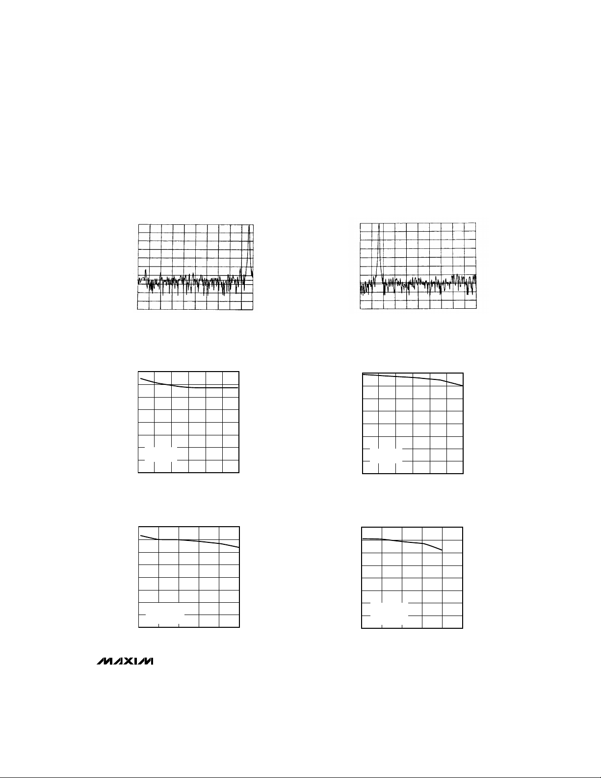
INTEGRAL NONLINEARITY
vs. OUTPUT CODE
0.75
0.50
0.25
0
INL (LSBs)
-0.25
-0.50
-0.75
0 64 128 192 256
OUTPUT CODE
DNL (LSBs)
-0.25
-0.50
-0.75
DIFFERENTIAL NONLINEARITY
vs. OUTPUT CODE
0.75
0.50
0.25
0
64 128 192 256
0
OUTPUT CODE
4 _______________________________________________________________________________________
Page 5
250Msps, 8-Bit ADC with Track/Hold
____________________________Typical Operating Characteristics (continued)
(TA = +25°C, unless otherwise noted.)
-10
-20
-30
0
FFT PLOT (f
= 120.4462MHz)
AIN
-40
-50
-60
-70
SIGNAL AMPLITUDE (dB)
-80
-90
-100
0
12.5 25 37.5 50 62.5 75 87.5 100 112.5125
FREQUENCY (MHz)
f
= 250MHz, f
CLK
SER = -42.3dB, NOISE FLOOR = -65.4dB
vs. ANALOG INPUT FREQUENCY
8
7
6
5
4
3
EFFECTIVE BITS
2
f
CLK
V
1
0
050
EFFECTIVE BITS
= 250MHz,
= 95% FS
IN
100 150
= 120.4462MHz
AIN
f
(MHz)
AIN
200
250 300
MAX100-10
FFT PLOT (f
0
-10
-20
-30
-40
-50
-60
-70
SIGNAL AMPLITUDE (dB)
-80
-90
-100
0 12.5
f
= 250MHz, f
CLK
SER = -45.87dB, NOISE FLOOR = -68.5dB
vs. CLOCK FREQUENCY
8
7
6
5
4
3
EFFECTIVE BITS
2
f
= 10.4MHz,
AIN
= 95% FS
V
IN
1
0
50
0
= 10.4462MHz)
AIN
37.5 50
25
FREQUENCY (MHz)
= 10.4462MHz
AIN
EFFECTIVE BITS
100 150 200 250
f
(MHz)
CLK
62.5
MAX100-11
300
MAX100
EFFECTIVE BITS
vs. ANALOG INPUT FREQUENCY
8
7
6
5
4
3
EFFECTIVE BITS
2
T
= +80°C,
CASE
= 250MHz,
f
CLK
1
= 95% FS
V
IN
0
050100 150 200 250
f
(MHz)
AIN
_______________________________________________________________________________________
MAX100-12
EFFECTIVE BITS
vs. ANALOG INPUT FREQUENCY
8
7
6
5
4
3
EFFECTIVE BITS
2
T
= -15°C,
CASE
= 250MHz
f
CLK
1
= 95% FS
V
IN
0
050
100 150 200 250
f
(MHz)
AIN
MAX100-13
5
Page 6
250Msps, 8-Bit ADC with Track/Hold
____________________________Typical Operating Characteristics (continued)
(TA = +25°C, unless otherwise noted.)
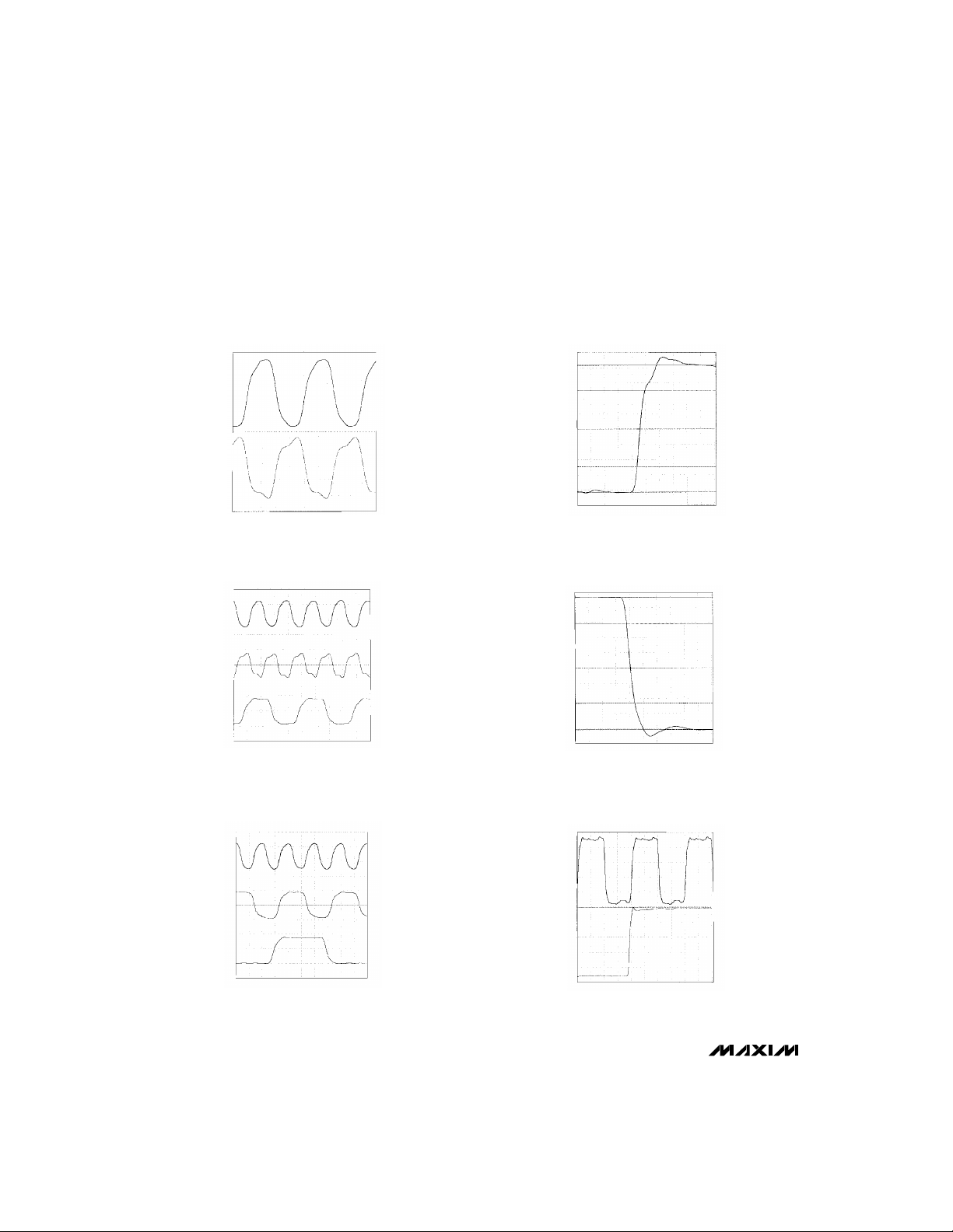
CLOCK RELATIONSHIP
(DIVIDE-BY-1 MODE)
DIGITAL CLOCK
(POSITIVE EDGE)
MAX100
A = CLK, 200mV/div
B = DCLK, 200mV/div
A = CLK, 500mV/div
B = DCLK, 500mV/div
C = AData, 500mV/div
TIMEBASE = 1ns/div,
f
CLK
CLOCK/DATA
(DIVIDE-BY-1 MODE)
TIMEBASE = 2ns/div,
f
= 250MHz
CLK
CLOCK/DATA
(DIVIDE-BY-2 MODE)
= 250MHz
A
DCLK
100mV/div
B
TIMEBASE = 1ns/div, tr = 580ps
DATA OUTPUT
(NEGATIVE EDGE)
A
B
C
TIMEBASE = 1ns/div, tf = 596ps
AData
OUTPUT
100mV/div
CLOCK/DATA DETAIL
(DIVIDE-BY-5 MODE)
A
B
C
A = CLK, 500mV/div
B = DCLK, 500mV/div
C = AData, 500mV/div
TIMEBASE = 2ns/div,
f
= 250MHz
CLK
A = DCLK, 200mV/div
B = AData, 200mV/div
TIMEBASE = 5ns/div,
f
= 250MHz
CLK
6 _______________________________________________________________________________________
A
B
Page 7
250Msps, 8-Bit ADC with Track/Hold
______________________________________________________________Pin Description
PIN
1 PAD Internal connection, leave open.
2, 62 CLK
3, 61 CLK
4, 7, 15, 49,
57, 60, 64,
67, 70, 71,
74, 77, 78,
79, 82, 84
5, 6, 9, 10,
31, 33, 35,
48, 58, 59,
63, 81, 83
8, 21, 43, 56 VCC Positive power supply, +5V ±5% nominal
11 DIV Divide Enable Input. DIV and MOD select the output modes. See Table 1.
12 MOD Modulus. MOD and DIV select the output modes. See Table 1.
13 DCLK
14 DCLK
16 A=B Sets AData equal to BData when asserted (A=B = 1). See Table 1.
17, 20, 23,
26, 36, 39,
42, 45
19, 22, 25,
28, 38, 41,
44, 47
NAME FUNCTION
Complementary Differential Clock Inputs. Can be driven from standard 10K ECL with the following
considerations: Internally, pins 2 & 62 and 3 & 61 are the ends of a 50Ω transmission line. Either end
can be driven, with the other end terminated with 50Ω to -2V. See
GND Power-Supply Ground. Connect GND and DGND pins (Note 10).
N.C. No Connect—there is no internal connection to these pins.
Complementary Differential Clock Outputs. Used to synchronize following circuitry: AData and BData
A7–A0
B7–B0
outputs are valid t
AData and BData Outputs. A0 and B0 are the LSBs, and A7 and B7 are the MSBs. AData and BData
outputs conform to standard 10K ECL logic swings and drive 50Ω transmission lines. Terminate with
50Ω to -2V. See Figures 1–4.
after the rising edge of DCLK. See Figures 1–4.
PD2
Typical Operating Circuit.
MAX100
18, 24, 27,
30, 34, 37,
40, 46
29 SUB
32, 69, 80 VEE Negative Power Supply, -5.2V ±5% nominal
50 VA
51 VA
DGND Power-Supply Ground. Connect all ground (GND, DGND) pins together, as described in Note 10.
Circuit Substrate Contact. This pin must be connected to VEE.
Positive Reference Voltage Input (Note 11)
RT
Positive Reference Voltage Sense (Note 11)
RTS
_______________________________________________________________________________________
7
Page 8

250Msps, 8-Bit ADC with Track/Hold
_________________________________________________Pin Description (continued)
NAME FUNCTIONPIN
52 VA
53 VA
MAX100
54 VA
55 VA
65 TP3 Internal node. Do not connect.
66 TP2 Internal node. Do not connect.
68 TP1
72, 73 AIN+
75, 76 AIN-
Reference Bias Resistor Center-Tap Sense (Note 12)
CTS
Reference Bias Resistor Center Tap (Note 12)
CT
Negative Reference Voltage Sense (Note 11)
RBS
Negative Reference Voltage Input (Note 11)
RB
Internal connection. This pin must be connected to GND.
Analog Inputs, internally terminated with 50Ω to ground. Full-scale linear input range is approximately
±270mV. Drive AIN+ and AIN- differentially for best high-frequency performance.
Note 10: Use a multilayer board with a separate layer dedicated to ground. Connect GND and DGND in separate areas in the
Note 11: Reference bias supply. Use a separate high-quality supply for these pins. Carefully bypassing these pins to achieve
Note 12: The center-tap connection of the MAX100 is normally left open. It can be driven with a bias voltage, but should be
ground plane (separated by at least 1/4 inch) and at only one location on the board (see
noise-free operation of the reference supplies contributes directly to high ADC accuracy.
bypassed carefully (refer to Note 11).
CLK
CLK
DCLK
DCLK
AData
BData
t
pwl
t
pd1
pd2
t
t
pwh
Typical Operating Circuit
).
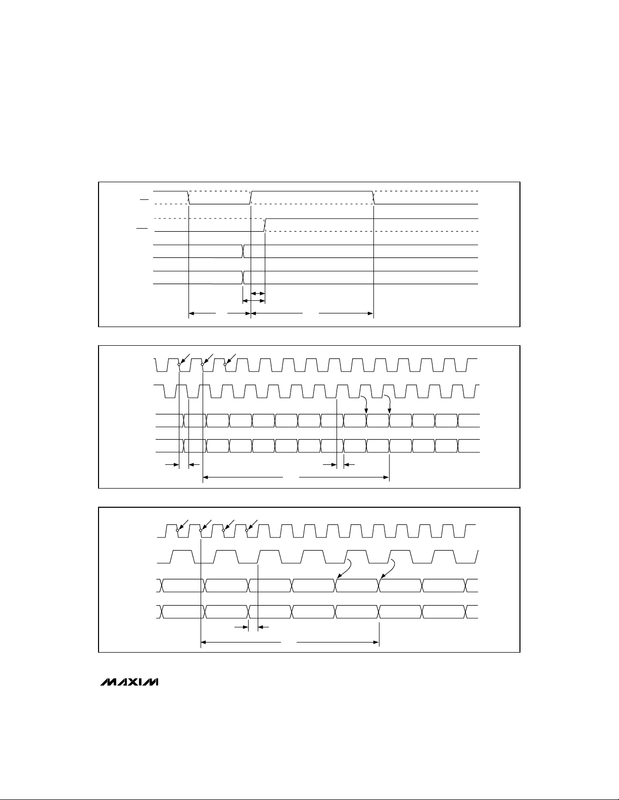
Figure 1. Output Timing: Divide-by-1 Mode (DIV = 0)
8 _______________________________________________________________________________________
Page 9
CLK
CLK
DCLK
DCLK
AData
250Msps, 8-Bit ADC with Track/Hold
MAX100
BData
pwl
t
pd1
t
pd2
t
t
pwh
Figure 2. Output Timing: Divide-by-2 or Divide-by-5 Mode (DIV = 1)
CLK
DCLK
AData
BData
N - 1 N N + 1
12345678
t
pd1
t
NPD
Figure 3. Output Timing: Clock to Data, Divide-by-1 Mode (fast mode, DIV = 0)
CLK
N - 1 N N + 1
12345
DCLK
N + 2N - 2
N - 1 N N + 1
N - 1 N N + 1
t
pd2
AData
BData
t
pd2
Figure 4. Output Timing: Divide-by-2 Mode (DIV = 1)
_______________________________________________________________________________________ 9
N - 1 N + 3
N - 2 N N + 2
t
NPD
N + 1
Page 10

250Msps, 8-Bit ADC with Track/Hold
______Definitions of Specifications
Signal-to-Noise Ratio and Effective Bits
Signal-to-noise ratio (SNR) is the ratio between the RMS
amplitude of the fundamental input frequency and the
RMS amplitude of all other analog-to-digital (A/D) output
signals. The theoretical minimum A/D noise is caused by
quantization error and is a direct result of the ADC’s reso-
MAX100
lution: SNR = (6.02N + 1.76)dB, where N is the number
of effective bits of resolution. Therefore, a perfect 8-bit
ADC can do no better than 50dB. The FFT plots in the
Typical Operating Characteristics
various spectral bands.
Effective bits is calculated from a digital record taken from
the ADC under test. The quantization error of the ideal
converter equals the total error of the device. In addition
to ideal quantization error, other sources of error include
all DC and AC nonlinearities, clock and aperture jitter,
missing output codes, and noise. Noise on references
and supplies also degrades effective bits performance.
The ADC’s input is a sine wave filtered with an anti-aliasing filter to remove any harmonic content. The digital
record taken from this signal is compared against a
mathematically generated sine wave. DC offsets, phase,
and amplitudes of the mathematical model are adjusted
until a best-fit sine wave is found. After subtracting this
sine wave from the digital record, the residual error
remains. The rms value of the error is applied in the following equation to yield the ADC’s effective bits.
Effective bits = N - log
where N is the resolution of the converter. In this case,
N = 8.
The worst-case error for any device will be at the converter’s maximum clock rate with the analog input near
the Nyquist rate (1/2 the input clock rate).
Aperture Width and Jitter
Aperture width is the time the T/H circuit takes to disconnect the hold capacitor from the input circuit (i.e., to
turn off the sampling bridge and put the T/H in hold
mode). Aperture jitter is the sample-to-sample variation
in aperture delay (Figure 5).
Errors resulting from metastable states may occur when
the analog input voltage, at the time the sample is
taken, falls close to the decision point for any one of the
input comparators. The resulting output code for many
show the output level in
measured rms error
—————————
2
(
ideal rms error
Error Rates
)
CLK
CLK
ANALOG
INPUT
t
AD
SAMPLED
DATA (T/H)
TRACK
T/H
Figure 5. T/H Aperture Timing
typical converters can be incorrect, including false fullor zero-scale output. The MAX100’s unique design
reduces the magnitude of this type of error to 1LSB,
and reduces the probability of the error occurring to
less than one in every 10
MAX100 were operated at 250MHz, 24 hours a day,
this would translate to less than one metastable-state
error every 46 days.
t
AW
t
AJ
APERTURE DELAY (t
APERTURE WIDTH (tAW)
APERTURE JITTER (tAJ)
AD)
15
clock cycles. If the
TRACKHOLD
Integral Nonlinearity
Integral nonlinearity (INL) is the deviation of the transfer
function from a reference line measured in fractions of
1LSB using a “best straight line” determined by a least
square curve fit.
Differential Nonlinearity
Differential nonlinearity (DNL) is the difference between
the measured LSB step and an ideal LSB step size
between adjacent code transitions. DNL is expressed
in LSBs and is calculated using the following equation:
[V
- (V
DNL(LSB) = —————————————
where V
code.
A DNL specification of less than 1LSB guarantees no
missing codes and a monotonic transfer function.
MEAS-1
MEAS
is the measured value of the previous
MEAS-1
LSB
)] - LSB
10 ______________________________________________________________________________________
Page 11
250Msps, 8-Bit ADC with Track/Hold
_______________Detailed Description
Converter Operation
The parallel or “flash” architecture used by the MAX100
provides the fastest multibit conversion of all common
integrated ADC designs. The basic element of a flash
(as with all other ADC architectures) is the comparator,
which has a positive input, a negative input, and an
output. If the voltage at the positive input is higher than
the negative input (connected to a reference), the output will be high. If the positive input voltage is lower
than the reference, the output will be low. A typical nbit flash consists of 2n-1 comparators with negative
inputs evenly spaced at 1LSB increments from the bottom to the top of the reference ladder. For n = 8, there
will be 255 comparators.
For any input voltage, all the comparators with negative
inputs connected to the reference ladder below the
input voltage will have outputs of 1, and all comparators with negative inputs above the input voltage will
have outputs of 0. Decode logic is provided to convert
this information into a parallel n-bit digital word (the output) corresponding to the number of LSBs (minus 1)
that the input voltage is above the level set at the bottom of the ladder.
Finally, the comparators contain latch circuitry and are
clocked. This allows the comparators to function as
described above when, for example, clock is low.
When clock goes high (samples) the comparator will
latch and hold its state until the clock goes low again.
Track/Hold
As with all ADCs, if the input waveform is changing
rapidly during the conversion the effective bits and
SNR will decrease. The MAX100 has an internal
track/hold (T/H) that increases attainable effective-bits
performance and allows more accurate capture of analog data at high conversion rates.
The internal T/H circuit provides two important circuit
functions for the MAX100:
1) Its nominal voltage gain of 4 reduces the input driving signal to ±270mV differential (assuming a
±1.02V reference).
2) It provides a differential 50Ω input that allows easy
interface to the MAX100.
Data Flow
The MAX100 contains an internal T/H amplifier that
stores the analog input voltage for the ADC to convert.
The differential inputs AIN+ and AIN- are tracked continuously between data samples. When a negative CLK
edge is applied, the T/H enters hold mode (Figure 5).
When CLK goes low, the most recent sample is presented to the ADC’s input comparators. Internal processing of the sampled data is delayed for several
clock cycles before it is available at outputs AData or
BData. All output data is timed with respect to DCLK
and DCLK
(Figures 1–4).
__________Applications Information
Although the normal operating range is ±270mV, the
MAX100 can be operated with up to ±500mV on each
input with respect to ground. This extended input level
includes the analog signal and any DC common-mode
voltage.
To obtain a full-scale digital output with differential input
drive, a nominal +270mV must be applied between
AIN+ and AIN-. That is, AIN+ = +135mV and AIN- =
-135mV (with no DC offset). Mid-scale digital output
code occurs when there is no voltage difference across
the analog inputs. Zero-scale digital output code, with
differential -270mV drive, occurs when AIN+ = -135mV
and AIN- = +135mV. Table 2 shows how the output of
the converter stays at all ones (full scale) when over
ranged or all zeros (zero scale) when under ranged.
For single-ended operation:
1) Apply a DC offset to one of the analog inputs, or
leave one input open. (Both AIN+ and AIN- are terminated internally with 50Ω to analog ground.)
2) Drive the other input with a ±270mV + offset to
obtain either full- or zero-scale digital output. If a DC
common-mode offset is used, the total voltage swing
allowed is ±500mV (analog signal plus offset with
respect to ground).
Table 1. Input Voltage Range
INPUT
Differential
Single
Ended
**An offset VIO, as specified in the DC electrical parameters, may
be present at the input. Compensate for this offset by either
adjusting the reference voltage (VARTor VARB), or introducing an
offset voltage in one of the input terminals AIN + or AIN-.
AIN+**
(mV)
+135 -135
0 0
-135 +135
+270 0
0 0
-270 0
Analog Input Ranges
AIN-**
(mV)
OUTPUT
CODE
11111111
10000000
00000000
11111111
10000000
00000000
MSB to LSB
full scale
mid scale
zero scale
full scale
mid scale
zero scale
MAX100
______________________________________________________________________________________ 11
Page 12

250Msps, 8-Bit ADC with Track/Hold
Table 2. Output Mode Control
MOD A=BDIV
0 X 0
MAX100
DCLK*
(MHz)
250
MODE
Divide
by 1
DESCRIPTION
Data appears on
AData only, BData
port inactive
(Figure 3).
POSITIVE
REFERENCE
VA
RT
VA
RTS
PARASITIC
RESISTANCE
0 X 1
250
Divide
by 1
AData identical to
BData (Figure 3).
8:16 demultiplexer
mode. AData
and BData ports
by 2
are active. BData
carries older
sample and
Divide
1251 0 0
AData carries
most recent sample (Figure 4).
AData and BData
ports are active,
by 2
both carry identical sampled data.
Alternate samples
Divide
1251 0 1
are taken but discarded.
AData port
updates data on
by 5
5th input CLK.
BData port inactive. Other 4 sam-
Divide
501 1 0
pled data points
are discarded.
AData and BData
ports are both
active with identical data. Data is
by 5
updated on output ports every
Divide
501 1 1
5th input clock
(CLK). The other
4 samples are
discarded.
*Input clocks (CLK, –C—L—K–) = 250MHz for all above combinations.
In divide-by-2 or divide-by-5 mode the output clock DCLK will
always be a 50% duty-cycle signal. In divide-by-1 mode DCLK
will have the same duty cycle as CLK.
VA
CT
VA
CTS
CENTER TAP
VA
RBS
VA
RB
NEGATIVE
REFERENCE
Figure 6. Reference Ladder String
R
TO
R
COMPARATORS
R
/
2
R
/
2
R
R
PARASITIC
RESISTANCE
12 ______________________________________________________________________________________
Page 13

250Msps, 8-Bit ADC with Track/Hold
The ADC’s reference resistor is a Kelvin-sensed, centertapped resistor string that sets the ADC’s LSB size and
dynamic operating range. Normally, the top and bottom of
this string are driven with an op amp, and the center tap is
left open. However, driving the center tap is an effective
way to modify the output coding to provide a user-defined
bilinear response. The buffer amplifier used to drive the
top and bottom inputs will need to supply approximately
18mA due to the resistor string impedance of 116Ω minimum. A reference voltage of ±1.02V is normally applied to
inputs VARTand VARB. This reference voltage can be
adjusted up to ±1.4V to accommodate extended input
requirements (accuracy specifications are guaranteed with
±1.02V references). The reference input VA
and VA
to increase precision.
An RC network at the ADC’s reference terminals is
needed for best performance. This network consists of
a 33Ω resistor connected in series with the op amp output that drives the reference. A 0.47µF capacitor must
be connected near the resistor at the op amp’s output
(see
capacitor combination should be located within 0.5
inches of the MAX100 package. Any noise on these
pins will directly affect the code uncertainty and
degrade the ADC’s effective-bits performance.
allow Kelvin sensing of the applied voltages
CTS
Typical Operating Circuit
). This resistor and
RTS
, VA
RBS
CLK and DCLK
All input and output clock signals are differential. The
input clocks, CLK and CLK, are the primary timing signals for the MAX100. CLK and CLK are fed to the internal circuitry from pins 2 & 3 or pins 62 & 61 through an
internal 50Ω transmission line. One pair of CLK/CLK
inputs should be driven and the other pair terminated
by 50Ω to -2V. Either pair can be used as the driven
inputs (input lines are balanced) for easy circuit con-
Reference
nection. A minimum pulse width (t
CLK and CLK (Figures 1–4).
For best performance and consistent results, use a low
phase-jitter clock source for CLK and CLK. Phase jitter
larger than 2ps from the input clock source reduces the
converter’s effective-bits performance and causes
inconsistent results.
) is required for
PWL
DCLK and DCLK
the input clocks and are used for external timing of the
AData and BData outputs. The MAX100 is characterized to work with maximum input clock frequencies of
250MHz (Table 1). See
are output clock signals derived from
Typical Operating Circuit.
Output Mode Control
DIV, MOD, and A=B are input pins that determine the
operating mode of the two output data paths. Six
options are available (Table 1). A typical operating configuration (8:16 demultiplexer mode) is set by 1 on DIV,
0 on MOD, and 0 on A=B. This will give the most
recent sample at AData with the older data on BData.
Both outputs are synchronous and are at half the input
clock rate. To terminate the control inputs, use a resis-
,
tor to -2V or the equivalent circuit resistor combination
from DGND to -5.2V up to 1kΩ. When using a diode
pull-up to tie an input high, bias the diode “on” with a
pull-down resistor to avoid input voltage excursions
close to ground. The control inputs are compatible with
standard ECL 10K logic levels over temperature.
Layout, Grounding, and Power Supplies
The MAX100 is designed with separate analog and digital ground connections to isolate high-current digital
noise spikes. The high-current digital ground, DGND,
is connected to the collectors of the output emitter follower transistors. The low-current ground connection is
GND, which is a combination of the analog ground and
the ground of the low-current digital decode section.
The DGND and GND connections should be at the
same DC level, and should be connected at only one
location on the board. This will provide better noise
immunity and highest device accuracy. A ground
plane is recommended.
A +5V ±5% supply as well as a -5.2V ±5% supply is
needed for proper operation. Bypass the VEE and
VCC supply pins to GND with high-quality 0.1µF and
0.001µF ceramic capacitors located as close to the
package as possible. An evaluation kit with a suggested layout is available.
MAX100
______________________________________________________________________________________ 13
Page 14

250Msps, 8-Bit ADC with Track/Hold
___________________________________________________Typical Operating Circuit
0.01µF
1
MX580LH
S
+V
2
VOUT
GND
MAX100
3
0.01µF
2.5V
50Ω
120Ω
150Ω
1.02V
20k
50k
70k
10k
1/2 MAX412
0.22µF
51Ω
20k
1/2 MAX412
0.22µF
20Ω
CMPSH-3
51Ω
20Ω 33Ω
CMPSH-3
50Ω
50
51
54
55
8, 21, 43, 56
VA
RT
VA
RTS
VA
CT
VA
CTS
VA
RBS
VA
RB
+5V
0.1µF
0.001µF
V
CC
AData
8
MC100E151
D>Q
Q
D>Q
Q
MC100E151
D>Q
Q
BData
8
D>Q
Q
MAX100
WATKINS-JOHNSON
SMRA 89-1
MC100E116
0.47µF
50Ω
-2V
50Ω
-2V
*PINS 68, 4, 7, 15, 49, 57, 60, 64
67, 70, 71, 74, 77, 78, 79,
82, 84, 18, 24, 27, 30, 34,
37, 40, 46
72. 73
AIN+
75, 76
AIN-
2
CLK
62
3
CLK
61
DGND GND SUB VEE
*
14
DCLK
13
DCLK
16
A=B
11
DIV
12
MOD
29 32, 69, 80
-5.2V
0.1µF
50Ω
1k
1k
1k
0.001µF
14 ______________________________________________________________________________________
-2V
CLOCK
-2V
-2V
-2V
10µF
Page 15
250Msps, 8-Bit ADC with Track/Hold
____________________________________________________________Pin Configuration
TOP VIEW
TP3
TP2
GND
65
64
63
N.C.
62
CLK
61
CLK
60
GND
59
N.C.
58
N.C.
57
GND
56
VCC
55
VA
RB
54
VA
RBS
53
VA
CT
52
VA
CTS
51
VA
RTS
50
VA
RT
49
GND
48
N.C.
47
B0
46
DGND
45
A0
44
B1
43
VCC
PAD
CLK
CLK
GND
N.C.
N.C.
GND
VCC
N.C.
N.C.
DIV
MOD
DCLK
DCLK
GND
A = B
DGND
VCC
AIN-
AIN-
GND
GND
N.C.
GND
84838281807978
1
2
3
4
5
6
7
8
9
10
11
12
13
14
15
16
17
A7
18
19
B7
20
A6
21
77
76
75
MAX100
74
GND
AIN+
73
GND
GND
VEE
N.C.
72
AIN+
GND
71
GND
70
VEE
69
GND
TP1
686766
MAX100
22
23
A5
B6
2425262728
A4
B5
DGND
DGND
29
B4
SUB
30
DGND
32
31
VEE
N.C.
35
33
34
N.C.
N.C.
DGND
38
37
36
A3
DGND
39
B3
A2
40
DGND
42
41
B2
A1
Ceramic Flat Pack
______________________________________________________________________________________ 15
Page 16
250Msps, 8-Bit ADC with Track/Hold
________________________________________________________Package Information
PIN FIN HEATSINK
FORCED CONVECTION PARAMETERS
23
MAX100
21
19
17
15
(°C/W)
JA
θ
13
11
45 Degrees*
12
7
0 100 200 300 400 500
*DIRECTION OF AIRFLOW ACROSS HEATSINK
0 Degrees*
VELOCITY (ft /min)
MAX100-insertB
E1
E
E2
e
S
0.060±.005(7x)
D1
D
D2
PIN #1
c
b
A2 A1
A
5–6°
E3
Maxim cannot assume responsibility for use of any circuitry other than circuitry entirely embodied in a Maxim product. No circuit patent licenses are
implied. Maxim reserves the right to change the circuitry and specifications without notice at any time.
16
__________________Maxim Integrated Products, 120 San Gabriel Drive, Sunnyvale, CA 94086 (408) 737-7600
© 1994 Maxim Integrated Products Printed USA is a registered trademark of Maxim Integrated Products.
0.060±.005
D3
0.075±.020(6x)
EQUAL SPACES
84 LEAD CERAMIC FLAT
PACK WITH HEAT SINK
MILLIMETERS INCHES
DIM
MIN MAX MIN MAX
A
17.272
A1
A2
b
C
D
D1
D2
D3
e
E
E1
E2
E3
S
18.288
1.041
1.270
3.048
3.302
0.406
0.508
0.228
0.279
29.184
29.794
44.196
44.704
25.298
25.502
28.448
28.829
1.270 BSC 0.050 BSC
29.184
29.794
44.196
44.704
25.298
25.502
28.194
28.702
1.930
2.184
0.680
0.041
0.120
0.016
0.009
1.149
1.740
0.996
1.120
1.149
1.740
0.996
1.110
0.076
0.720
0.050
0.130
0.020
0.011
1.173
1.760
1.004
1.135
1.173
1.760
1.004
1.130
0.086
 Loading...