

Page 1
General Description
The LMX331/LMX393/LMX339 single/dual/quad comparators are drop-in, pin-for-pin-compatible replacements for the LMV331/LMV393/LMV339. The LMX331H/
LMX393H/LMX339H offer the performance of the
LMX331/LMX393/LMX339 with the added benefit of internal hysteresis to provide noise immunity, preventing output oscillations even with slow-moving input signals.
Advantages of the LMX331/LMX393/LMX339 series
include low supply voltage, small package, and low cost.
The LMX331 is available in both 5-pin SC70 and SOT23
packages, LMX393 is available in both 8-pin µMAX and
smaller SOT23 packages, and the LMX339 is available in
14-pin TSSOP and SO packages. They are manufactured using advanced submicron CMOS technology.
Designed with the most modern techniques, the
LMX331/LMX393/LMX339 achieve superior performance
over BiCMOS or bipolar versions on the market.
The LMX331/LMX393/LMX339 offer performance
advantages such as wider supply voltage range, wider
operating temperature range, better CMRR and PSRR,
improved response time characteristics, reduced offset, reduced output saturation voltage, reduced input
bias current, and improved RF immunity.
Applications
Mobile Communications
Notebooks and PDAs
Automotive Applications
Battery-Powered Electronics
General-Purpose Portable Devices
General-Purpose Low-Voltage Applications
Features
♦ Guaranteed 1.8V to 5.5V Performance
♦ -40°C to +125°C Automotive Temperature Range
♦ Low Supply Current (60µA/Comparator at
V
DD
= 5.0V)
♦ Input Common-Mode Voltage Range Includes
Ground
♦ No Phase Reversal for Overdriven Inputs
♦ Low Output Saturation Voltage (100mV)
♦ Internal 2mV Hysteresis
(LMX331H/LMX393H/LMX339H)
♦ 5-Pin SC70 Space-Saving Package
(2.0mm
✕
2.1mm ✕1.0mm)
(LMX331/LMX331H)
LMX331/LMX393/LMX339
General-Purpose, Low-Voltage,
Single/Dual/Quad, Tiny-Pack Comparators
________________________________________________________________ Maxim Integrated Products 1
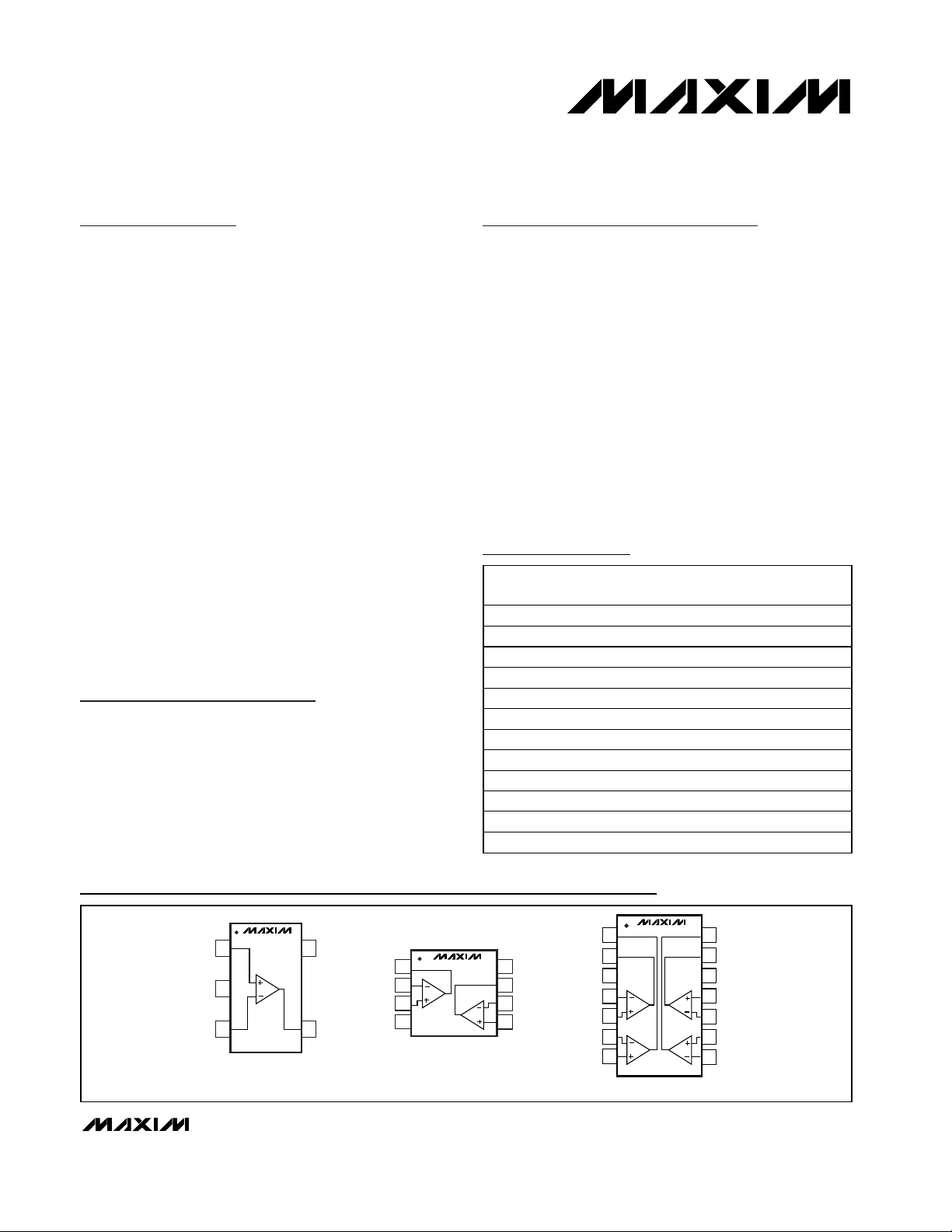
Pin Configurations
19-1958; Rev 2; 1/02
For pricing, delivery, and ordering information, please contact Maxim/Dallas Direct! at
1-888-629-4642, or visit Maxim’s website at www.maxim-ic.com.
Ordering Information
LMX331AXK-T -40°C to +125°C 5 SC70-5 ACD
LMX331AUK-T -40°C to +125°C 5 SOT23-5 ADQR
LMX331HAXK-T
LMX331HAUK-T -40°C to +125°C 5 SOT23-5 ADQS
LMX393AKA-T -40°C to +125°C 8 SOT23-8 AAIF
LMX393AUA -40°C to +125°C 8 µMAX —
LMX393HAKA-T -40°C to +125°C 8 SOT23-8 AAIG
LMX393HAUA -40°C to +125°C 8 µMAX —
LMX339AUD -40°C to +125°C 14 TSSOP —
LMX339ASD -40°C to +125°C 14 SO —
LMX339HAUD -40°C to +125°C 14 TSSOP —
LMX339HASD -40°C to +125°C 14 SO —
PART TEMP RANGE
-40°C to +125°C
PINPACKAGE
TOP
MARK
5 SC70-5 ACE
TOP VIEW
LMX331/LMX331H
15V
IN+
2
V
SS
34
SC70/SOT23
DD
OUTA
INA-
INA+
OUTIN-
SS
LMX393/LMX393H
1
2
A
3
4
SOT23/µMAX
8
V
DD
7
OUTB
INB-
6
B
INB+V
5
OUTB
OUTA
V
INA-
INA+
INB-
1
2
DD
3
4
5
6
7
LMX339/LMX339H
AD
BC
TSSOP/SO
14
13
12
11
10
OUTC
OUTD
V
SS
IND+
IND-
INC+
9
INC-INB+
8
Page 2
LMX331/LMX393/LMX339
General-Purpose, Low-Voltage,
Single/Dual/Quad, Tiny-Pack Comparators
2 _______________________________________________________________________________________
ABSOLUTE MAXIMUM RATINGS
DC ELECTRICAL CHARACTERISTICS—2.7V OPERATION
(VDD= 2.7V, VSS= 0, VCM= 0, RL= 5.1kΩ connected to VDD. Typical values are at TA= +25°C.) (Note 1)
Stresses beyond those listed under “Absolute Maximum Ratings” may cause permanent damage to the device. These are stress ratings only, and functional
operation of the device at these or any other conditions beyond those indicated in the operational sections of the specifications is not implied. Exposure to
absolute maximum rating conditions for extended periods may affect device reliability.
Supply Voltage (VDDto VSS)...................................-0.3V to +6V
All Other Pins .................................. (V
SS
- 0.3V) to (VDD+ 0.3V)
Continuous Power Dissipation (TA= +70°C)
5-Pin SC70 (derate 3.1mW/°C above +70°C)..............247mW
5-Pin SOT23 (derate 7.1mW/°C above +70°C)............571mW
8-Pin SOT23 (derate 8.9mW/°C above +70°C)............714mW
8-Pin µMAX (derate 10.3mW/°C above +70°C) ...........825mW
14-Pin TSSOP (derate 9.1mW/°C above +70°C) .........727mW
14-Pin SO (derate 8.3mW/°C above +70°C).............666.7mW
Operating Temperature Range .........................-40°C to +125°C
Junction Temperature......................................................+150°C
Storage Temperature Range .............................-65°C to +150°C
Lead Temperature (soldering, 10s) .................................+300°C
PARAMETER
CONDITIONS
UNITS
Input Offset Voltage V
OS
0.2 7 mV
Input Voltage Hysteresis V
HYST
LMX331H/LMX393H/LMX339H only 2 mV
Input Offset Voltage Average
Temperature Drift
5
µV/°C
TA = +25°C
TA = -40°C to +85°C
Input Bias Current I
B
TA = -40°C to +125°C
nA
TA = +25°C
TA = -40°C to +85°C
Input Offset Current I
OS
TA = -40°C to +125°C
nA
Input Voltage Range V
CM
2.0
V
Voltage Gain A
V
LMX331/LMX393/LMX339 only 50
V/mV
Output Saturation Voltage V
SATISINK
≤ 1mA 50 mV
Output Sink Current I
O
VO ≤ 1.5V 5 37 mA
LMX331/LMX331H 50
LMX393/LMX393H (both comparators) 70
Supply Current (Note 2) I
S
LMX339/LMX339H (all four comparators)
µA
TA = +25°C
TA = -40°C to +85°C1Output Leakage Current
T
A
= -40°C to +125°C2
µA
AC ELECTRICAL CHARACTERISTICS—2.7V OPERATION
(VDD= 2.7V, VSS= 0, VCM= 0, RL= 5.1kΩ connected to VDD. Typical values are at TA= +25°C.) (Note 1)
SYMBOL
TCV
OS
MIN TYP MAX
±0.05 ±250
±400
±400
±0.05 ±50
±150
±150
-0.1
Propagation Delay
Output High to Low
Propagation Delay
Output Low to High
PARAMETER SYMBOL CONDITIONS MIN TYP MAX UNITS
140 200
t
PHL
t
PLH
Input overdrive = 10mV (Note 3) 500
Input overdrive = 100mV (Note 3) 100
Input overdrive = 10mV (Note 3) 500
Input overdrive = 100mV (Note 3)
0.003
100
100
140
ns
ns
Page 3
LMX331/LMX393/LMX339
General-Purpose, Low-Voltage,
Single/Dual/Quad, Tiny-Pack Comparators
_______________________________________________________________________________________ 3
DC ELECTRICAL CHARACTERISTICS—5.0V OPERATION
(VDD= 5V, VSS= 0, VCM= 0, RL= 5.1kΩ connected to VDD. Typical values are at TA= +25°C.) (Note 1)
AC ELECTRICAL CHARACTERISTICS—5.0V OPERATION
(VDD= 5V, VSS= 0, VCM= 0, RL= 5.1kΩ connected to VDD. Typical values are at TA= +25°C.) (Note 1)
PARAMETER
SYMBOL
CONDITIONS
MIN
TYP
MAX
UNITS
Input overdrive = 10mV (Note 3)
Propagation Delay
Output High to Low
t
PHL
Input overdrive = 100mV (Note 3) 90
ns
Input overdrive = 10mV (Note 3)
Propagation Delay
Output Low to High
t
PLH
Input overdrive = 100mV (Note 3)
ns
Input Offset Voltage V
Input Voltage Hysteresis LMX331H/LMX393H/LMX339H only 2 mV
Input Offset Voltage Average
Temperature Drift
Input Offset Current I
Input Voltage Range V
Voltage Gain A
Output Sink Current I
Supply Current (Note 2) I
PARAMETER SYMBOL CONDITIONS MIN TYP MAX UNITS
TA = +25°C 0.25 7
TA = -40°C to +85°C9
OS
TA = -40°C to +125°C9
TCV
OS
B
OS
CM
V
SATISINK
O
S
TA = +25°C ±0.05 ±250
TA = -40°C to +85°C ±400Input Bias Current I
TA = -40°C to +125°C ±400
TA = +25°C ±0.05 ±50
TA = -40°C to +85°C ±150
TA = -40°C to +125°C ±150
LMX331/LMX393/LMX339 only 20 50 V/mV
TA = +25°C 70 400
≤ 4mA
VO ≤ 1.5V 10 73 mA
LMX393/LMX393H
(both comparators)
LMX339/LMX339H
(all four comparators)
TA = +25°C 0.003
TA = -40°C to +85°C1Output Leakage Current
= -40°C to +125°C2
T
A
TA = -40°C to +85°C 700Output Saturation Voltage V
= -40°C to +125°C 700
T
A
TA = +25°C 60 120
TA = -40°C to +85°C 150LMX331/LMX331H
= -40°C to +125°C 170
T
A
TA = +25°C 100 200
TA = -40°C to +85°C 250
T
= -40°C to +125°C 300
A
TA = +25°C 170 300
TA = -40°C to +85°C 350
= -40°C to +125°C 430
T
A
5 µV/°C
-0.1
4.2
mV
nA
nA
V
mV
µA
µA
400
600
200
Page 4
LMX331/LMX393/LMX339
General-Purpose, Low-Voltage,
Single/Dual/Quad, Tiny-Pack Comparators
4 _______________________________________________________________________________________
DC ELECTRICAL CHARACTERISTICS—1.8V OPERATION
(VDD= 1.8V, VSS= 0, VCM= 0, RL= 5.1kΩ connected to VDD. Typical values are at TA= +25°C.)
PARAMETER
SYMBOL
CONDITIONS
MIN
TYP
MAX
UNITS
Input Offset Voltage V
OS
0.2 5 mV
Input Voltage Hysteresis LMX331H/LMX393H/LMX339H only 2 mV
Input Offset Voltage Average
Temperature Drift
5
µV/°C
Input Bias Current I
B
nA
Input Offset Current I
OS
nA
Input Voltage Range V
CM
1
V
Output Saturation Voltage V
SATISINK
≤ 1mA 35 mV
Power-Supply Rejection Ratio PSRR VDD = 1.8V to 5.5V 60 70 dB
Output Sink Current I
O
V
O
≤ 1.5V 15 mA
LMX331/LMX331H 40
LMX393/LMX393H (both comparators) 65
Supply Current (Note 2) I
S
LMX339/LMX339H (all four comparators)
µA
Output Leakage Current
µA
Note 1: All devices are production tested at +25°C. All temperature limits are guaranteed by design.
Note 2: Supply current when output is high.
Note 3: Input overdrive is the overdrive voltage beyond the offset and hysteresis-determined trip points.
AC ELECTRICAL CHARACTERISTICS—1.8V OPERATION
(VDD= 1.8V, VSS= 0, VCM= 0, RL= 5.1kΩ connected to VDD. Typical values are at TA= +25°C.)
PARAMETER
SYMBOL
CONDITIONS
MIN
TYP
MAX
UNITS
Input overdrive = 10mV (Note 3)
Propagation Delay
Output High to Low
t
PHL
Input overdrive = 100mV (Note 3)
ns
Input overdrive = 10mV (Note 3)
Propagation Delay
Output Low to High
t
PLH
Input overdrive = 100mV (Note 3)
ns
TCV
OS
0.05
0.05
-0.1
120 200
0.003
100
140
500
100
500
100
Page 5

LMX331/LMX393/LMX339
General-Purpose, Low-Voltage,
Single/Dual/Quad, Tiny-Pack Comparators
_______________________________________________________________________________________ 5
Typical Operating Characteristics
(V
DD
= 5V, VSS= 0, VCM= 0, RL= 5.1kΩ, CL= 10pF, overdrive = 100mV, TA= +25°C, unless otherwise noted.)
SUPPLY CURRENT vs. SUPPLY VOLTAGE
100
90
80
70
60
50
40
30
SUPPLY CURRENT (µA)
20
10
0
TA = +125°C
TA = +85°C
TA = +25°C
TA = -40°C
V
= HIGH
OUT
132 456
SUPPLY VOLTAGE (V)
OUTPUT LOW VOLTAGE vs. SINK CURRENT
140
120
LMX331
100
80
60
40
OUTPUT LOW VOLTAGE (mV)
20
0
01234
V
V
= 1.8V
DD
SINK CURRENT (mA)
= 2.7V
DD
V
= 5.0V
DD
180
160
LMX331 toc01
140
120
100
80
60
SUPPLY CURRENT (µA)
40
20
0
OUTPUT LOW VOLTAGE vs. TEMPERATURE
120
LMX331 toc04
110
100
90
80
OUTPUT LOW VOLTAGE (mV)
70
60
SUPPLY CURRENT vs. SUPPLY VOLTAGE
TA = +85°C
V
= LOW
OUT
132 456
I
OUT
-40 0-20 20 40 60 80 100 120
LMX331
TA = +125°C
TA = +25°C
SUPPLY VOLTAGE (V)
= 4mA
TEMPERATURE (°C)
TA = -40°C
1.5
LMX331 toc02
1.0
0.5
0
INPUT OFFSET VOLTAGE (mV)
-0.5
-1.0
-40 0 20-20 40 60 80 100 120
PROPAGATION DELAY vs. CAPACITIVE LOAD
600
LMX331 toc05
500
400
300
200
PROPAGATION DELAY (ns)
100
0
0406020 80 100 120
INPUT OFFSET VOLTAGE
vs. TEMPERATURE
V
= 5.0V
DD
V
= 2.7V
DD
V
= 1.8V
DD
TEMPERATURE (°C)
t
CAPACITIVE LOAD (pF)
PHL
LMX331 toc03
LMX331 toc06
t
PLH
PROPAGATION DELAY vs. TEMPERATURE
175
150
125
100
75
50
PROPAGATION DELAY (ns)
25
0
-40 0 20-20 40 60 80 100 120
TEMPERATURE (°C)
t
PLH
t
PHL
500
450
LMX331 toc07
400
350
300
250
200
150
PROPAGATION DELAY (ns)
100
50
0
PROPAGATION DELAY
vs. INPUT OVERDRIVE (t
TA = -40°C
TA = +25°C
TA = +85°C
TA = +125°C
05025 75 100 125 150
INPUT OVERDRIVE (mV)
PLH
)
200
180
LMX331 toc08
160
140
120
100
80
60
PROPAGATION DELAY (ns)
40
20
0
05025 75 100 125 150
PROPAGATION DELAY
vs. INPUT OVERDRIVE (t
TA = -40°C
TA = +25°C
TA = +125°C
TA = +85°C
INPUT OVERDRIVE (mV)
PHL
)
LMX331 toc09
Page 6

LMX331/LMX393/LMX339
General-Purpose, Low-Voltage,
Single/Dual/Quad, Tiny-Pack Comparators
6 _______________________________________________________________________________________
Typical Operating Characteristics (continued)
(V
DD
= 5V, VSS= 0, VCM= 0, RL= 5.1kΩ, CL= 10pF, overdrive = 100mV, TA= +25°C, unless otherwise noted.)
0
0.5
1.0
1.5
2.0
2.5
3.0
-40 0-20 20 40 60 80 100 120
LMX331H/LMX393H/LMX339H
HYSTERESIS vs. TEMPERATURE
LMX331 toc10
TEMPERATURE (°C)
HYSTERESIS (mV)
0
1
3
2
4
5
132456
LMX331H/LMX393H/LMX339H
HYSTERESIS vs. SUPPLY VOLTAGE
LMX331 toc11
SUPPLY VOLTAGE (V)
HYSTERESIS (mV)
TIME (200ns/div)
(IN-) - IN+
100mV/div
OUT
2V/div
LMX331 toc12
PROPAGATION DELAY
100mV OVERDRIVE
TIME (200ns/div)
(IN-) - IN+
10mV/div
OUT
2V/div
LMX331 toc13
PROPAGATION DELAY
10mV OVERDRIVE
TIME (500ns/div)
(IN-) - IN+
100mV/div
OUT
2V/div
LMX331 toc14
500kHz RESPONSE
100mV OVERDRIVE
TIME (500ns/div)
(IN-) - IN+
10mV/div
OUT
2V/div
LMX331 toc15
500kHz RESPONSE
10mV OVERDRIVE
TIME (2µs/div)
(IN-) - IN+
100mV/div
OUT
2V/div
LMX331 toc16
100kHz RESPONSE
100mV OVERDRIVE
TIME (2µs/div)
(IN-) - IN+
10mV/div
OUT
2V/div
LMX331 toc17
100kHz RESPONSE
10mV OVERDRIVE
TIME (1µs/div)
V
DD
2V/div
OUT
2V/div
LMX331 toc18
POWER-UP RESPONSE
Page 7

LMX331/LMX393/LMX339
General-Purpose, Low-Voltage,
Single/Dual/Quad, Tiny-Pack Comparators
_______________________________________________________________________________________ 7
Detailed Description
The LMX331/LMX393/LMX339 are single/dual/quad,
low-cost, general-purpose comparators. They have a
single-supply operating voltage of 1.8V to 5V. The common-mode input range extends from -0.1V below the
negative supply to within 0.7V of the positive supply.
They require approximately 60µA per comparator with
a 5V supply and 40µA with a 2.7V supply.
The LMX331H/LMX393H/LMX339H have 2mV of hysteresis for noise immunity. This significantly reduces the
chance of output oscillations even with slow-moving
input signals. The LMX331/LMX393/LMX339 and
LMX331H/LMX393H/LMX339H are ideal for automotive
applications because they operate from -40°C to
+125°C (see Typical Operating Characteristics).
Applications Information
Hysteresis
Many comparators oscillate in the linear region of operation because of noise or undesired parasitic feedback. This tends to occur when the voltage on one
input is equal or very close to the voltage on the other
input. The LMX331H/LMX393H/LMX339H have internal
hysteresis to counter parasitic effects and noise.
The hysteresis in a comparator creates two trip points:
one for the rising input voltage and one for the falling
input voltage (Figure 1). The difference between the trip
points is the hysteresis. When the comparator's input
voltages are equal, the hysteresis effectively causes
one comparator input to move quickly past the other,
thus taking the input out of the region where oscillation
occurs. This provides clean output transitions for noisy,
slow-moving input signals.
Additional hysteresis can be generated with two resistors, using positive feedback (Figure 2). Use the following procedure to calculate resistor values:
Figure 1. Threshold Hysteresis Band (Not to Scale)
PIN
LMX331
LMX393 LMX339
NAME FUNCTION
1 —— IN+ Noninverting Input
2 4 12 V
SS
Negative Supply (Connect to GND)
3 —— IN- Inverting Input
4 —— OUT Comparator Output (Open-Drain)
583VDDPositive Supply
— 1 2 OUTA Comparator A Output (Open-Drain)
— 7 1 OUTB Comparator B Output (Open-Drain)
— 2 4 INA- Comparator A Inverting Input
— 3 5 INA+ Comparator A Noninverting Input
— 5 7 INB+ Comparator B Noninverting Input
— 6 6 INB- Comparator B Inverting Input
—— 8 INC- Comparator C Inverting Input
—— 9 INC+ Comparator C Noninverting Input
—— 10 IND- Comparator D Inverting Input
—— 11 IND+ Comparator D Noninverting Input
—— 13 OUTD Comparator D Output (Open-Drain)
—— 14 OUTC Comparator C Output (Open-Drain)
Pin Description
IN+
IN-
OUT
THRESHOLDS
V
HYSTERESIS
V
HYST
BAND
TH
V
TL
Page 8

LMX331/LMX393/LMX339
General-Purpose, Low-Voltage,
Single/Dual/Quad, Tiny-Pack Comparators
8 _______________________________________________________________________________________
1) Find output voltage when output is high:
V
OUT(HIGH)
= VDD- I
LOAD
✕
R
L
2) Find the trip points of the comparator using these
formulas:
VTH= V
REF
+ ((V
OUT
(HIGH)
- V
REF
)R2) / (R1 + R2)
VTL= V
REF
(1 - (R2 / (R1 + R2)))
where VTHis the threshold voltage at which the comparator switches its output from high to low as VINrises
above the trip point, and VTLis the threshold voltage at
which the comparator switches its output from low to
high as VINdrops below the trip point.
3) The hysteresis band will be:
V
HYST
= VTH- VTL= VDD(R2 / (R1 + R2))
In this example, let V
DD
= 5V, V
REF
= 2.5V, I
LOAD
=
50nA, RL= 5.1kΩ:
V
OUT(HIGH)
= 5.0V - (50 ✕10
-9
✕
5.1 ✕103Ω) ≈ 5.0V
VTH= 2.5V + 2.5V(R2 / (R1 + R2))
VTL= 2.5V(1 - (R2 / (R1 + R2)))
Select R2. In this example, we will choose 1kΩ.
Select V
HYST
. In this example, we will choose 50mV.
Solve for R1:
V
HYST
= V
OUT(HIGH)
(R2 / (R1 + R2)) V
0.050V = 5(1000 / (R1 + 1000)) V
where R1 ≈ 100kΩ, V
TH
= 2.525V, and VTL= 2.475V.
Choose R1 and R2 to be large enough as not to exceed
the amount of current the reference can supply.
The source current required is V
REF
/ (R1 + R2).
The sink current is (V
OUT(HIGH)
- V
REF
) ✕(R1 + R2).
Choose RLto be large enough to avoid drawing excess
current, yet small enough to supply the necessary current to drive the load. RLshould be between 1kΩ and
10kΩ.
Board Layout and Bypassing
Use 0.1µF bypass capacitors from VDDto VSS. To maximize performance, minimize stray inductance by
putting this capacitor close to the VDDpin and reducing trace lengths. For slow-moving input signals (rise
time > 1ms), use a 1nF capacitor between IN+ and INto reduce high-frequency noise.
Chip Information
LMX331/LMX331H TRANSISTOR COUNT: 112
LMX393/LMX393H TRANSISTOR COUNT: 211
LMX339/LMX339H TRANSISTOR COUNT: 411
Figure 2. Adding Hysteresis with External Resistors
V
DD
R1
V
DD
V
R2
REF
V
IN
IN+
IN-
V
SS
R
L
LMX331
OUT
V
OUT
Page 9

LMX331/LMX393/LMX339
General-Purpose, Low-Voltage,
Single/Dual/Quad, Tiny-Pack Comparators
_______________________________________________________________________________________ 9
Package Information
SC70, 5L.EPS
SOT5L.EPS
Page 10

LMX331/LMX393/LMX339
General-Purpose, Low-Voltage,
Single/Dual/Quad, Tiny-Pack Comparators
10 ______________________________________________________________________________________
Package Information (continued)
SOT23, 8L.EPS
8LUMAXD.EPS
Page 11

LMX331/LMX393/LMX339
General-Purpose, Low-Voltage,
Single/Dual/Quad, Tiny-Pack Comparators
______________________________________________________________________________________ 11
Package Information (continued)
TSSOP,NO PADS.EPS
Page 12

LMX331/LMX393/LMX339
General-Purpose, Low-Voltage,
Single/Dual/Quad, Tiny-Pack Comparators
Maxim cannot assume responsibility for use of any circuitry other than circuitry entirely embodied in a Maxim product. No circuit patent licenses are
implied. Maxim reserves the right to change the circuitry and specifications without notice at any time.
12 ____________________Maxim Integrated Products, 120 San Gabriel Drive, Sunnyvale, CA 94086 408-737-7600
© 2002 Maxim Integrated Products Printed USA is a registered trademark of Maxim Integrated Products.
Package Information (continued)
SOICN.EPS
 Loading...