

Page 1
LM99
±
1˚C Accurate, High Temperature, Remote Diode
Temperature Sensor with Two-Wire Interface
General Description
The LM99 is an 11-bit remote diode temperature sensor with
a 2-wire System Management Bus (SMBus) serial interface.
The LM99 accurately measures: (1) its own temperature and
(2) the temperature of a remote diode-connected transistor
such as the 2N3904 or a thermal diode commonly found on
Graphics Processor Units (GPU), Computer Processor Units
(CPU or other ASICs. The LM99 remote diode temperature
sensor shifts the temperature from the remote sensor down
16˚C and operates on that shifted temperature:
T
ACTUAL DIODE JUNCTION
The local temperature reading requires no offset.
The LM99 has an Offset Register which provides a means
for precise matching to various thermal diodes. Contact
hardware.monitor
The LM99 and LM99-1 have the same functions but different
SMBus slave addresses. This allows for one of each to be on
the same bus at the same time.
Activation of the ALERT output occurs when any temperature goes outside a preprogrammed window set by the HIGH
and LOW temperature limit registers or exceeds the T_CRIT
temperature limit. Activation of the T_CRIT_A occurs when
any temperature exceeds the T_CRIT programmed limit.
@
nsc.com for the latest details.
=T
LM99
+ 16˚C
Features
n Accurately senses the temperature of remote diodes
n Offset register allows use of a variety of thermal diodes
n On-board local temperature sensing
n 10 bit plus sign remote diode temperature data format,
0.125 ˚C resolution
n T_CRIT_A output useful for system shutdown
n ALERT output supports SMBus 2.0 protocol
n SMBus 2.0 compatible interface, supports TIMEOUT
n 8-pin MSOP package
Key Specifications
j
Supply Voltage 3.0 V to 3.6 V
j
Supply Current 0.8 mA (typ)
j
Local Temp Accuracy (includes quantization error)
T
= 25˚C to 125˚C
A
j
Remote Diode Temp Accuracy (includes quantization
error)
= 30˚C to 50˚C, TD= 120˚C to 140˚C
T
A
T
= 0˚C to 85˚C, TD= 25˚C to 140˚C
A
Applications
n Graphics Processor Thermal Management
n Computer Processor Thermal Management
n Electronic Test Equipment
n Office Electronics
July 2003
±
3.0˚C (max)
±
1.0˚C (max)
±
3.0˚C (max)
Interface
LM99
±
1˚C Accurate, High Temperature, Remote Diode Temperature Sensor with Two-Wire
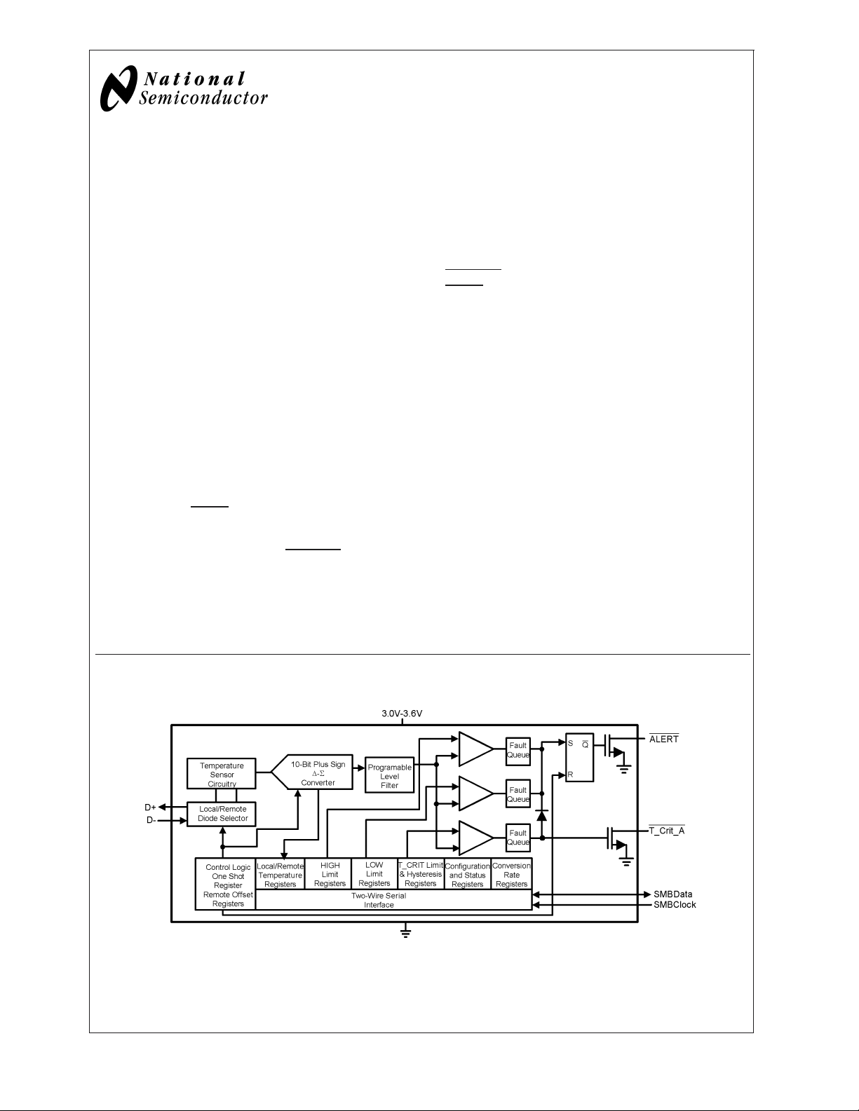
Simplified Block Diagram
20053801
NVIDIA®is a registered trademark of NVIDIA Corporation.
™
GeForce
is a trademark of NVIDIA Corporation.
®
Intel
and Pentium®are registered trademarks of Intel Corporation.
© 2003 National Semiconductor Corporation DS200538 www.national.com
Page 2
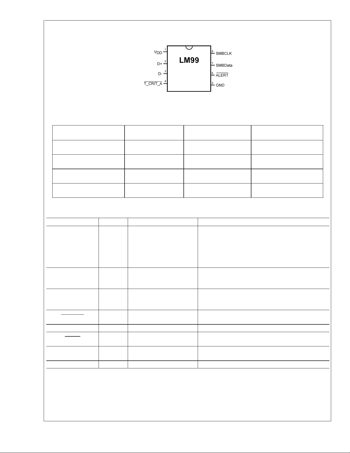
Connection Diagram
LM99
MSOP-8
TOP VIEW
20053802
Ordering Information
Part Number
LM99CIMM T17C
LM99-1CIMM T20C
LM99CIMMX T17C
LM99-1CIMMX T20C
Package
Marking
NS Package
Number
MUA08A
(MSOP-8)
MUA08A
(MSOP-8)
MUA08A
(MSOP-8)
MUA08A
(MSOP-8)
Pin Descriptions
Label Pin
V
DD
D+ 2 Diode Current Source
D− 3 Diode Return Current Sink
T_CRIT_A
GND 5 Power Supply Ground Ground
ALERT
SMBData 7
SMBCLK 8 SMBus Input From Controller, Pull-Up Resistor
#
1 Positive Supply Voltage Input
4
6
T_CRIT Alarm Output,
Open-Drain, Active-Low
Interrupt Output, Open-Drain,
Active-Low
SMBus Bi-Directional Data
Line, Open-Drain Output
Function Typical Connection
DC Voltage from 3.0 V to 3.6 V. V
with a 0.1 µF capacitor in parallel with 100 pF to ground.
The 100 pF capacitor should be placed as close as
possible to the power supply pin. A bulk capacitance of
approximately 10 µF needs to be in the vicinity of the LM99
.
V
DD
To Diode Anode. Connected to the collector and base of
the remote discrete diode-connected transistor. Connect a
2.2 nF capacitor between pins 2 and 3.
To Diode Cathode. Connects to the emitter of the remote
diode-connected transistor. Connect a 2.2 nF capacitor
between pins 2 and 3.
Pull-Up Resistor, Controller Interrupt or Power Supply
Shutdown Control
Pull-Up Resistor, Controller Interrupt or Alert Line
From and to Controller, Pull-Up Resistor
Transport
Media
1000 Units on
Tape and Reel
1000 Units on
Tape and Reel
3500 Units on
Tape and Reel
3500 Units on
Tape and Reel
should be bypassed
DD
www.national.com 2
Page 3
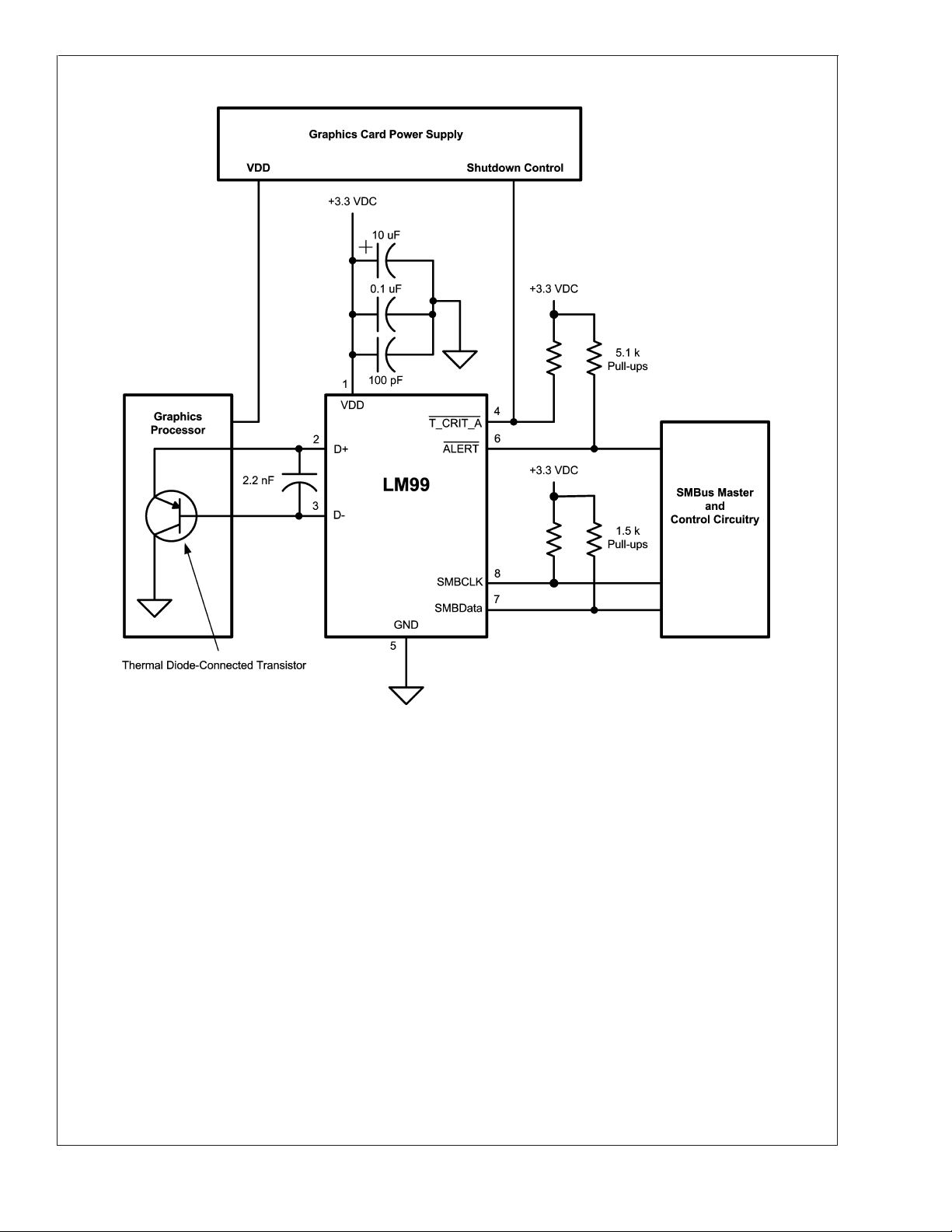
Typical Application
LM99
20053803
www.national.com3
Page 4
Absolute Maximum Ratings (Note 1)
LM99
Supply Voltage −0.3 V to 6.0 V
Voltage at SMBData, SMBCLK,
ALERT, T_CRIT_A
Voltage at Other Pins −0.3 V to
D− Input Current
Input Current at All Other Pins
(Note 2)
Package Input Current
(Note 2)
SMBData, ALERT, T_CRIT_A Output
Sink Current 10 mA
Storage Temperature −65˚C to
−0.5 V to 6.0 V
+ 0.3 V)
(V
DD
±
1mA
±
5mA
30 mA
+150˚C
MSOP-8 Packages (Note 3)
Vapor Phase (60 seconds) 215˚C
Infrared (15 seconds) 220˚C
ESD Susceptibility (Note 4)
Human Body Model 2000 V
Machine Model 200 V
Operating Ratings
(Notes 1, 5)
Operating Temperature Range 0˚C to +125˚C
Electrical Characteristics
Temperature Range T
LM99 0˚C ≤ TA≤ +85˚C
Supply Voltage Range (V
) +3.0 V to +3.6 V
DD
MIN
Soldering Information, Lead Temperature
Temperature-to-Digital Converter Characteristics
Unless otherwise noted, these specifications apply for VDD= +3.0 Vdc to +3.6 Vdc. Boldface limits apply for TA=TJ=T
≤ TA≤ T
Temperature Error Using Local Diode T
Temperature Error Using Remote Diode
Connected Transistor (TDis the Remote
Diode Junction Temperature)
T
D=TLM99
Remote Diode Measurement Resolution 11 Bits
Local Diode Measurement Resolution 8 Bits
Conversion Time of All Temperatures at the
Fastest Setting
Quiescent Current (Note 9) SMBus Inactive, 16 Hz
D− Source Voltage 0.7 V
Diode Source Current (V
ALERT and T_CRIT_A Output Saturation
Voltage
Power-On-Reset (POR) Threshold Measure on VDDinput, falling
Local and Remote HIGH Default Temperature
settings
Local and Remote LOW Default Temperature
settings
Local T_CRIT Default Temperature Setting (Note 11) +85 ˚C
Remote T_CRIT Default Temperature Setting (Note 11) Add 16˚C for 126˚C
; all other limits TA=TJ= +25˚C, unless otherwise noted.
MAX
Parameter Conditions Typical Limits Units
(Note 6) (Note 7) (Limit)
+ 16˚C
= +25˚C to +125˚C, (Note 8)
A
= +30˚C to +50˚C and TD=
T
A
+120˚C to +140˚C
T
= +0˚C to +85˚C and TD=
A
+25˚C to +140˚C
±
1
±
3 ˚C (max)
±
1 ˚C (max)
±
3
0.125 ˚C
1˚C
(Note 10) 31.25 34.4 ms (max)
0.8 1.7 mA (max)
conversion rate
Shutdown 315 µA
D+−VD−
level
) = + 0.65 V; high
160 315 µA (max)
110 µA (min)
Low level 13 20 µA (max)
7 µA (min)
I
= 6.0 mA 0.4
OUT
2.4
edge
(Note 11) Add 16˚C for true
+70 ˚C
1.8
Remote Temperature.
(Note 11) Add 16˚C for true
0˚C
Remote Temperature.
+110 ˚C
true Remote T_CRIT Setting
≤ TA≤ T
˚C (max)
V (max)
V (max)
V (min)
MAX
MIN
www.national.com 4
Page 5
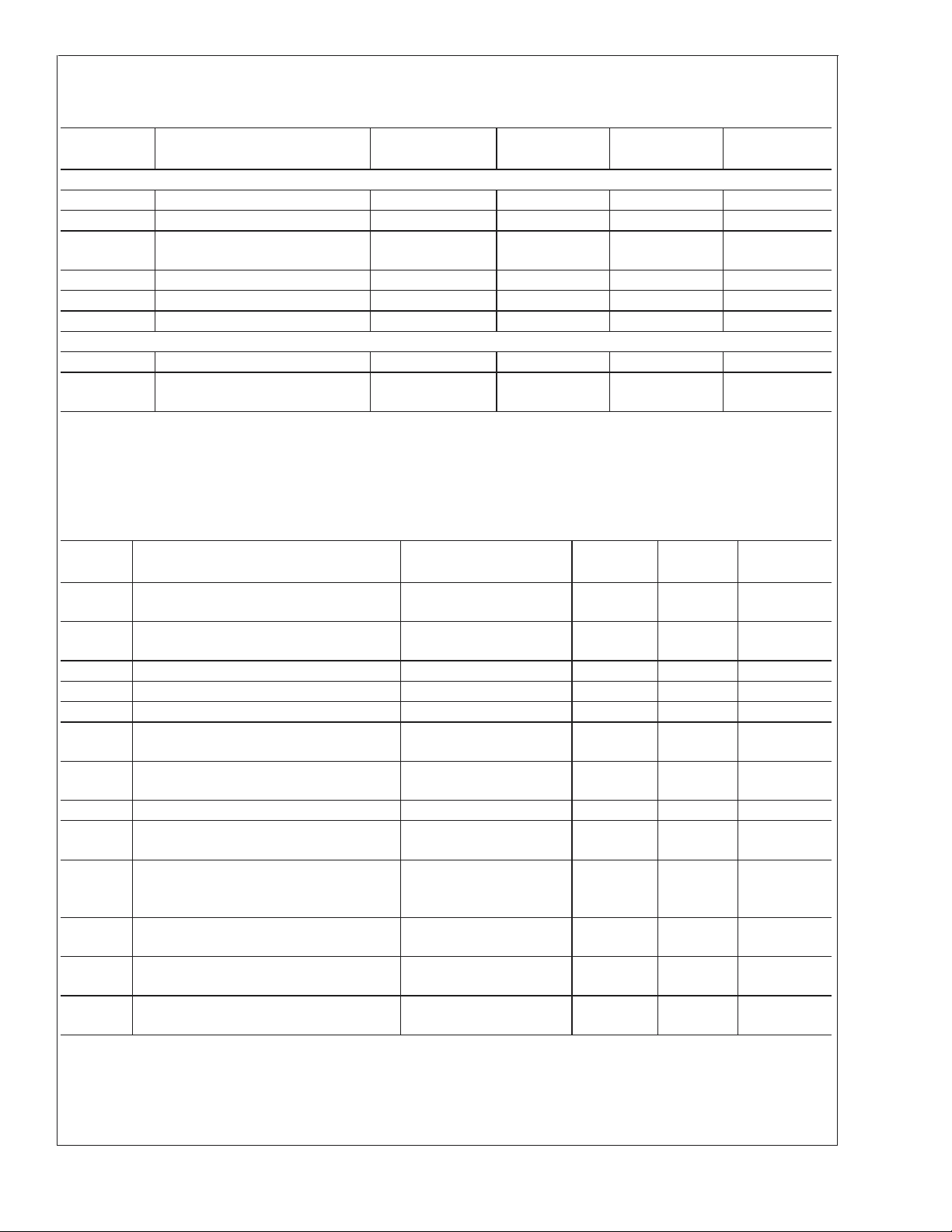
Logic Electrical Characteristics
DIGITAL DC CHARACTERISTICS Unless otherwise noted, these specifications apply for VDD= +3.0 to 3.6 Vdc. Boldface
to T
limits apply for T
A=TJ=TMIN
; all other limits TA=TJ= +25˚C, unless otherwise noted.
MAX
Symbol Parameter Conditions Typical Limits Units
(Note 6) (Note 7) (Limit)
SMBData, SMBCLK INPUTS
V
V
IN(1)
IN(0)
V
IN(HYST)
Logical “1” Input Voltage 2.1 V (min)
Logical “0”Input Voltage 0.8 V (max)
SMBData and SMBCLK Digital
400 mV
Input Hysteresis
I
I
C
IN(1)
IN(0)
IN
Logical “1” Input Current VIN=V
DD
0.005
Logical “0” Input Current VIN= 0 V −0.005
Input Capacitance 5 pF
±
10 µA (max)
±
10 µA (max)
ALL DIGITAL OUTPUTS
I
OH
V
OL
High Level Output Current VOH=V
DD
SMBus Low Level Output Voltage IOL=4mA
=6mA
I
OL
10 µA (max)
0.4
V (max)
0.6
SMBus Digital Switching Characteristics
Unless otherwise noted, these specifications apply for VDD= +3.0 Vdc to +3.6 Vdc, CL(load capacitance) on output lines = 80
to T
pF. Boldface limits apply for T
A=TJ=TMIN
ing characteristics of the LM99 fully meet or exceed the published specifications of the SMBus version 2.0. The following parameters are the timing relationships between SMBCLK and SMBData signals related to the LM99. They adhere to but are not
necessarily the SMBus bus specifications.
Symbol Parameter Conditions Typical Limits Units
f
SMB
t
LOW
t
HIGH
t
R,SMB
t
F,SMB
t
OF
t
TIMEOUT
SMBus Clock Frequency 100
SMBus Clock Low Time from V
SMBus Clock High Time from V
SMBus Rise Time (Note 12) 1 µs (max)
SMBus Fall Time (Note 13) 0.3 µs (max)
Output Fall Time CL= 400 pF,
SMBData and SMBCLK Time Low for
Reset of Serial Interface (Note 14)
t
SU;DAT
t
HD;DAT
t
HD;STA
Data In Setup Time to SMBCLK High 250 ns (min)
Data Out Stable after SMBCLK Low 300
Start Condition SMBData Low to SMBCLK
Low (Start condition hold before the first
clock falling edge)
t
SU;STO
Stop Condition SMBCLK High to SMBData
Low (Stop Condition Setup)
t
SU;STA
SMBus Repeated Start-Condition Setup
Time, SMBCLK High to SMBData Low
t
BUF
SMBus Free Time Between Stop and Start
Conditions
; all other limits TA=TJ= +25˚C, unless otherwise noted. The switch-
MAX
(Note 6) (Note 7) (Limit)
kHz (max)
10
max to
IN(0)
max
V
IN(0)
IN(1)
min to V
min 4.0 µs (min)
IN(1)
4.7
25
kHz (min)
ms (max)
250 ns (max)
= 3 mA, (Note 13)
I
O
25
35
ms (max)
900
100 ns (min)
100 ns (min)
0.6 µs (min)
1.3 µs (min)
µs (min)
ms (min)
ns (min)
ns (max)
LM99
www.national.com5
Page 6
SMBus Communication
LM99
Note 1: Absolute Maximum Ratings indicate limits beyond which damage to the device may occur. DC and AC electrical specifications do not apply when operating
the device beyond its rated operating conditions.
Note 2: When the input voltage (V
Parasitic components and or ESD protection circuitry are shown in the figure below for the LM99’s pins. The nominal breakdown voltage of D3 is 6.5 V. Care should
be taken not to forward bias the parasitic diode, D1, present on pins: D+, D−. Doing so by more than 50 mV may corrupt a temperature measurement.
) at any pin exceeds the power supplies (V
I
<
GND or V
I
>
VDD), the current at that pin should be limited to 5 mA.
I
20053840
Pin Name PIN
V
DD
#
D1 D2 D3 D4 D5 D6 D7 R1 SNP ESD CLAMP
1 x
D+ 2 xx xxx x
D− 3 xx xxx x
T_CRIT_A
ALERT
4xxx
6xxx
SMBData 7 x x x
SMBCLK 8 x
Note: An “x” indicates that the diode exists.
20053813
FIGURE 1. ESD Protection Input Structure
Note 3: See the URL ”http://www.national.com/packaging/“ for other recommendations and methods of soldering surface mount devices.
Note 4: Human body model, 100 pF discharged through a 1.5 kΩ resistor. Machine model, 200 pF discharged directly into each pin.
Note 5: Thermal resistance junction-to-ambient when attached to a printed circuit board with 2 oz. foil:
– MSOP-8 = 210˚C/W
Note 6: Typicals are at T
Note 7: Limits are guaranteed to National’s AOQL (Average Outgoing Quality Level).
Note 8: Local temperature accuracy does not include the effects of self-heating. The rise in temperature due to self-heating is the product of the internal power
dissipation of the LM99 and the thermal resistance. See (Note 5) for the thermal resistance to be used in the self-heating calculation.
Note 9: Quiescent current will not increase substantially with an SMBus.
Note 10: This specification is provided only to indicate how often temperature data is updated. The LM99 can be read at any time without regard to conversion state
(and will yield last conversion result).
Note 11: Default values set at power up.
Note 12: The output rise time is measured from (V
Note 13: The output fall time is measured from (V
Note 14: Holding the SMBData and/or SMBCLK lines Low for a time interval greater than t
SMBData and SMBCLK pins to a high impedance state.
= 25˚C and represent most likely parametric norm.
A
max + 0.15 V) to (V
IN(0)
min - 0.15 V) to (V
IN(1)
min − 0.15 V).
IN(1)
min + 0.15 V).
IN(1)
will reset the LM99’s SMBus state machine, therefore setting
TIMEOUT
www.national.com 6
Page 7

1.0 Functional Description
The LM99 temperature sensor incorporates a delta V
based temperature sensor using a Local or Remote diode
and a 10-bit plus sign ∆Σ ADC (Delta-Sigma Analog-toDigital Converter). The LM99 is compatible with the serial
SMBus version 2.0 two-wire interface. Digital comparators
compare the measured Local Temperature (LT) to the Local
High (LHS), Local Low (LLS) and Local T_CRIT (LCS) userprogrammable temperature limit registers. The measured
Remote Temperature (RT) is digitally compared to the Remote High (RHS), Remote Low (RLS) and Remote T_CRIT
(RCS) user-programmable temperature limit registers. Activation of the ALERT output indicates that a comparison is
greater than the limit preset in a T_CRIT or HIGH limit
register or less than the limit preset in a LOW limit register.
The T_CRIT_A output responds as a true comparator with
built in hysteresis. The hysteresis is set by the value placed
in the Hysteresis register (TH). Activation of T_CRIT_A occurs when the temperature is above the T_CRIT setpoint.
T_CRIT_A remains activated until the temperature goes below the setpoint calculated by T_CRIT − TH. The hysteresis
register impacts both the remote temperature and local temperature readings.
The LM99 may be placed in a low power consumption
(Shutdown) mode by setting the RUN/STOP bit found in the
Configuration register. In the Shutdown mode, the LM99’s
SMBus interface remains while all circuitry not required is
turned off.
The Local temperature reading and setpoint data registers
are 8-bits wide. The format of the 11-bit remote temperature
data is a 16-bit left justified word. Two 8-bit registers, high
and low bytes, are provided for each setpoint as well as the
temperature reading. Two offset registers (RTOLB and
RTOHB) can be used to compensate for non–ideality error,
discussed further in Section 4.1 DIODE NON-IDEALITY.
The remote temperature reading reported is adjusted by
subtracting from, or adding to, the actual temperature reading the value placed in the offset register.
1.1 CONVERSION SEQUENCE
The LM99 takes approximately 31.25 ms to convert the
Local Temperature (LT), Remote Temperature (RT), and to
update all of its registers. Only during the conversion process the busy bit (D7) in the Status register (02h) is high.
These conversions are addressed in a round–robin sequence. The conversion rate may be modified by the Conversion Rate Register (04h). When the conversion rate is
modified a delay is inserted between conversions; however,
the actual conversion time remains at 31.25 ms. Different
conversion rates will cause the LM99 to draw different
amounts of supply current as shown in Figure 2.
BE
LM99
20053839
FIGURE 2. Conversion Rate Effect on Power Supply
Current
1.2 THE ALERT OUTPUT
The LM99’s ALERT pin is an active-low open-drain output
that is triggered by a temperature conversion that is outside
the limits defined by the temperature setpoint registers. Reset of the ALERT output is dependent upon the selected
method of use. The LM99’s ALERT pin is versatile and will
accommodate three different methods of use to best serve
the system designer: as a temperature comparator, as a
temperature–based interrupt flag, and as part of an SMBus
ALERT system. The three methods of use are further described below. The ALERT and interrupt methods are different only in how the user interacts with the LM99.
Each temperature reading (LT and RT) is associated with a
T_CRIT setpoint register (LCS, RCS), a HIGH setpoint register (LHS and RHS) and a LOW setpoint register (LLS and
RLS). At the end of every temperature reading, a digital
comparison determines whether that reading is above its
HIGH or T_CRIT setpoint or below its LOW setpoint. If so,
the corresponding bit in the STATUS REGISTER is set. If the
ALERT mask bit is not high, any bit set in the STATUS
REGISTER, with the exception of Busy (D7) and OPEN
(D2), will cause the ALERT output to be pulled low. Any
temperature conversion that is out of the limits defined by the
temperature setpoint registers will trigger an ALERT. Additionally, the ALERT mask bit in the Configuration register
must be cleared to trigger an ALERT in all modes.
1.2.1 ALERT Output as a Temperature Comparator
When the LM99 is implemented in a system in which it is not
serviced by an interrupt routine, the ALERT output could be
used as a temperature comparator. Under this method of
use, once the condition that triggered the ALERT to go low is
no longer present, the ALERT is de-asserted (Figure 3). For
example, if the ALERT output was activated by the comparison of LT>LHS, when this condition is no longer true the
ALERT will return HIGH. This mode allows operation without
software intervention, once all registers are configured during set-up. In order for the ALERT to be used as a temperature comparator, bit D0 (the ALERT configure bit) in the
FILTER and ALERT CONFIGURE REGISTER (xBF) must
be set high. This is not the power on default default state.
www.national.com7
Page 8

1.0 Functional Description (Continued)
LM99
20053828
20053831
FIGURE 3. ALERT Comparator Temperature Response
Diagram
1.2.2 ALERT Output as an Interrupt
The LM99’s ALERT output can be implemented as a simple
interrupt signal when it is used to trigger an interrupt service
routine. In such systems it is undesirable for the interrupt flag
to repeatedly trigger during or before the interrupt service
routine has been completed. Under this method of operation,
during a read of the STATUS REGISTER the LM99 will set
the ALERT mask bit (D7 of the Configuration register) if any
bit in the STATUS REGISTER is set, with the exception of
Busy (D7) and OPEN (D2). This prevents further ALERT
triggering until the master has reset the ALERT mask bit, at
the end of the interrupt service routine. The STATUS REGISTER bits are cleared only upon a read command from the
master (see Figure 4) and will be re-asserted at the end of
the next conversion if the triggering condition(s) persist(s). In
order for the ALERT to be used as a dedicated interrupt
signal, bit D0 (the ALERT configure bit) in the FILTER and
ALERT CONFIGURE REGISTER (xBF) must be set low.
This is the power–on default state.
The following sequence describes the response of a system
that uses the ALERT output pin as a interrupt flag:
1. Master Senses ALERT low
2. Master reads the LM99 STATUS REGISTER to determine what caused the ALERT
3. LM99 clears STATUS REGISTER, resets the ALERT
HIGH and sets the ALERT mask bit (D7 in the Configuration register).
4. Master attends to conditions that caused the ALERT to
be triggered. The fan is started, setpoint limits are adjusted, etc.
5. Master resets the ALERT mask (D7 in the Configuration
register).
FIGURE 4. ALERT Output as an Interrupt Temperature
Response Diagram
1.2.3 ALERT Output as an SMBus ALERT
When the ALERT output is connected to one or more ALERT
outputs of other SMBus compatible devices and to a master,
an SMBus alert line is created. Under this implementation,
the LM99’s ALERT should be operated using the ARA (Alert
Response Address) protocol. The SMBus 2.0 ARA protocol,
defined in the SMBus specification 2.0, is a procedure designed to assist the master in resolving which part generated
an interrupt and service that interrupt while impeding system
operation as little as possible.
The SMBus alert line is connected to the open-drain ports of
all devices on the bus thereby AND’ing them together. The
ARA is a method by which with one command the SMBus
master may identify which part is pulling the SMBus alert line
LOW and prevent it from pulling it LOW again for the same
triggering condition. When an ARA command is received by
all devices on the bus, the devices pulling the SMBus alert
line LOW, first, send their address to the master and second,
release the SMBus alert line after recognizing a successful
transmission of their address.
The SMBus 1.1 and 2.0 specification state that in response
to an ARA (Alert Response Address) “after acknowledging
the slave address the device must disengage its SMBALERT
pulldown”. Furthermore, “if the host still sees SMBALERT
low when the message transfer is complete, it knows to read
the ARA again”. This SMBus “disengaging of SMBALERT”
requirement prevents locking up the SMBus alert line. Competitive parts may address this “disengaging of SMBALERT”
requirement differently than the LM99 or not at all. SMBus
systems that implement the ARA protocol as suggested for
the LM99 will be fully compatible with all competitive parts.
The LM99 fulfills “disengaging of SMBALERT” by setting the
ALERT mask bit (bit D7 in the Configuration register, at
address 09h) after successfully sending out its address in
response to an ARA and releasing the ALERT output pin.
Once the ALERT mask bit is activated, the ALERT output pin
will be disabled until enabled by software. In order to enable
the ALERT the master must read the STATUS REGISTER,
at address 02h, during the interrupt service routine and then
reset the ALERT mask bit in the Configuration register to 0 at
the end of the interrupt service routine.
The following sequence describes the ARA response protocol.
www.national.com 8
Page 9

1.0 Functional Description (Continued)
1. Master Senses SMBus alert line low
2. Master sends a START followed by the Alert Response
Address (ARA) with a Read Command.
3. Alerting Device(s) send ACK.
4. Alerting Device(s) send their Address. While transmitting
their address, alerting devices sense whether their address has been transmitted correctly. (The LM99 will
reset its ALERT output and set the ALERT mask bit once
its complete address has been transmitted successfully.)
5. Master/slave NoACK
6. Master sends STOP
7. Master attends to conditions that caused the ALERT to
be triggered. The STATUS REGISTER is read and fan
started, setpoint limits adjusted, etc.
8. Master resets the ALERT mask (D7 in the Configuration
register).
The ARA, 000 1100, is a general call address. No device
should ever be assigned this address.
Bit D0 (the ALERT configure bit) in the FILTER and ALERT
CONFIGURE REGISTER (xBF) must be set low in order for
the LM99 to respond to the ARA command.
The ALERT output can be disabled by setting the ALERT
mask bit, D7, of the Configuration register. The power on
default is to have the ALERT mask bit and the ALERT
configure bit low.
LM99
reset only after the Status Register is read and if a temperature conversion(s) is/are below the T_CRIT setpoint, as
shown in Figure 6.
20053806
FIGURE 6. T_CRIT_A Temperature Response Diagram
1.4 POWER ON RESET DEFAULT STATES
LM99 always powers up to these known default states. The
LM99 remains in these states until after the first conversion.
1. Command Register set to 00h
2. Local Temperature set to 0˚C
3. Remote Diode Temperature set to 0˚C until the end of
the first conversion.
4. Status Register set to 00h.
5. Configuration register set to 00h; ALERT enabled, Remote T_CRIT alarm enabled and Local T_CRIT alarm
enabled
6. 85˚C Local T_CRIT temperature setpoint
7. 110˚C Remote T_CRIT temperature setpoint (126˚C Remote diode junction temperature)
8. 70˚C Local and Remote HIGH temperature setpoints
9. 0˚C Local and Remote LOW temperature setpoints
10. Filter and Alert Configure Register set to 00h; filter dis-
abled, ALERT output set as an SMBus ALERT
11. Conversion Rate Register set to 8h; conversion rate set
to 16 conv./sec.
20053829
FIGURE 5. ALERT Output as an SMBus ALERT
Temperature Response Diagram
1.3 T_CRIT_A OUTPUT and T_CRIT LIMIT
T_CRIT_A is activated when any temperature reading is
greater than the limit preset in the critical temperature setpoint register (T_CRIT), as shown in Figure 6. The Status
Register can be read to determine which event caused the
alarm. A bit in the Status Register is set high to indicate
which temperature reading exceeded the T_CRIT setpoint
temperature and caused the alarm, see Section 2.3.
Local and remote temperature diodes are sampled in sequence by the A/D converter. The T_CRIT_A output and the
Status Register flags are updated after every Local and
Remote temperature conversion. T_CRIT_A follows the
state of the comparison, it is reset when the temperature falls
below the setpoint RCS-TH. The Status Register flags are
1.5 SMBus INTERFACE
The LM99 operates as a slave on the SMBus, so the
SMBCLK line is an input and the SMBData line is bidirectional. The LM99 never drives the SMBCLK line and it
does not support clock stretching. According to SMBus
specifications, the LM99 has a 7-bit slave address. All bits A6
through A0 are internally programmed and can not be
changed by software or hardware. The LM99 and LM99-1
have the following slave addresses:
Version A6 A5 A4 A3 A2 A1 A0
LM99 1001100
LM99-1 1001101
1.6 TEMPERATURE DATA FORMAT
Temperature data can only be read from the Local and
Remote Temperature registers; the setpoint registers
(T_CRIT, LOW, HIGH) are read/write.
www.national.com9
Page 10

1.0 Functional Description (Continued)
LM99
Remote temperature data is represented by an 11-bit, two’s
complement word with an LSB (Least Significant Bit) equal
Actual vs. LM99 Remote Temperature Conversion
Actual Remote Diode
Temperature,˚C
120 +104 0110 1000 0000 0000 6800h
125 +109 0110 1101 0000 0000 6D00h
126 +110 0110 1110 0000 0000 7100h
130 +114 0111 0010 0010 0000 7200h
135 +119 0111 0111 0000 0000 7700h
140 +124 0111 1100 0000 0000 7200h
Output is 11-bit two’s complement word. LSB = 0.125 ˚C.
Actual Remote Diode
T_Crit Setpoint,˚C
126 +110 0110 1110 71h
LM99 Remote Diode
Temperature Register, ˚C
Actual vs. Remote T_Crit Setpoint
Factory-Programmed
Remote T_CRIT High
Setpoint, ˚C
to 0.125˚C. The data format is a left justified 16-bit word
available in two 8-bit registers:
Binary Results in LM99
Remote Temperature Register
Binary Remote T_CRIT High
Setpoint Value
Hex Remote
Temperature
Register
Hex Remote T_CRIT
High Setpoint Value
Local Temperature data is represented by an 8-bit, two’s
complement byte with an LSB (Least Significant Bit)
equal to 1˚C:
Local
Temperature
+125˚C 0111 1101 7Dh
+25˚C 0001 1001 19h
+1˚C 0000 0001 01h
0˚C 0000 0000 00h
−1˚C 1111 1111 F F h
−25˚C 1110 0111 E7h
−55˚C 1100 1001 C9h
1.7 OPEN-DRAIN OUTPUTS
The SMBData, ALERT and T_CRIT_A outputs are opendrain outputs and do not have internal pull-ups. A “high” level
will not be observed on these pins until pull-up current is
provided by some external source, typically a pull-up resistor. Choice of resistor value depends on many system factors but, in general, the pull-up resistor should be as large as
possible. This will minimize any internal temperature reading
errors due to internal heating of the LM99. The maximum
resistance of the pull-up to provide a 2.1V high level, based
on LM99 specification for High Level Output Current with the
supply voltage at 3.0V, is 82 kΩ (5%) or 88.7 kΩ (1%).
Digital Output
Binary Hex
1.8 DIODE FAULT DETECTION
The LM99 is equipped with operational circuitry designed to
detect fault conditions concerning the remote diode. In the
event that the D+ pin is detected as shorted to V
floating, the Remote Temperature High Byte (RTHB) register
is loaded with +127˚C, the Remote Temperature Low Byte
(RTLB) register is loaded with 0, and the OPEN bit (D2) in
the status register is set. As a result, if the Remote T_CRIT
setpoint register (RCS) is set to a value less than +127˚C the
ALERT and T_Crit output pins will be pulled low, if the Alert
Mask and T_Crit Mask are disabled. If the Remote HIGH
Setpoint High Byte Register (RHSHB) is set to a value less
than +127˚C then ALERT will be pulled low, if the Alert Mask
is disabled. The OPEN bit itself will not trigger and ALERT.
In the event that the D+ pin is shorted to ground or D−, the
Remote Temperature High Byte (RTHB) register is loaded
with −128˚C (1000 0000) and the OPEN bit (D2) in the status
register will not be set. Since operating the LM99 at −128˚C
is beyond it’s operational limits, this temperature reading
represents this shorted fault condition. If the value in the
Remote Low Setpoint High Byte Register (RLSHB) is more
than −128˚C and the Alert Mask is disabled, ALERT will be
pulled low.
Remote diode temperature sensors that have been previously released and are competitive with the LM99 output a
code of 0˚C if the external diode is short-circuited. This
change is an improvement that allows a reading of 0˚C to be
truly interpreted as a genuine 0˚C reading and not a fault
condition.
DD
or
www.national.com 10
Page 11

1.0 Functional Description (Continued)
1.9 COMMUNICATING WITH THE LM99
The data registers in the LM99 are selected by the Command Register. At power-up the Command Register is set to
“00”, the location for the Read Local Temperature Register.
The Command Register latches the last location it was set
to. Each data register in the LM99 falls into one of four types
of user accessibility:
1. Read only
2. Write only
3. Read/Write same address
4. Read/Write different address
A Write to the LM99 will always include the address byte and
the command byte. A write to any register requires one data
byte.
Reading the LM99 can take place either of two ways:
1. If the location latched in the Command Register is correct (most of the time it is expected that the Command
LM99
Register will point to one of the Read Temperature Registers because that will be the data most frequently read
from the LM99), then the read can simply consist of an
address byte, followed by retrieving the data byte.
2. If the Command Register needs to be set, then an
address byte, command byte, repeat start, and another
address byte will accomplish a read.
The data byte has the most significant bit first. At the end of
a read, the LM99 can accept either Acknowledge or No
Acknowledge from the Master (No Acknowledge is typically
used as a signal for the slave that the Master has read its
last byte). It takes the LM99 31.25 ms to measure the
temperature of the remote diode and internal diode. When
retrieving all 10 bits from a previous remote diode temperature measurement, the master must insure that all 10 bits are
from the same temperature conversion. This may be
achieved by using one-shot mode or by setting the conversion rate and monitoring the busy bit such that no conversion
occurs in between reading the MSB and LSB of the last
temperature conversion.
www.national.com11
Page 12

1.0 Functional Description (Continued)
LM99
1.9.1 SMBus Timing Diagrams LM99 Timing Diagram
(a) Serial Bus Write to the internal Command Register followed by a the Data Byte
20053810
(b) Serial Bus Write to the Internal Command Register
20053811
(c) Serial Bus Read from a Register with the Internal Command Register preset to desired value.
20053812
FIGURE 7. SMBus Timing Diagrams
1.10 SERIAL INTERFACE RESET
In the event that the SMBus Master is RESET while the
LM99 is transmitting on the SMBData line, the LM99 must be
returned to a known state in the communication protocol.
This may be done in one of two ways:
1. When SMBData is LOW, the LM99 SMBus state machine resets to the SMBus idle state if either SMBData
or SMBCLK are held low for more than 35 ms (t
). Note that according to SMBus specification 2.0 all
EOUT
www.national.com 12
TIM
-
devices are to timeout when either the SMBCLK or
SMBData lines are held low for 25-35 ms. Therefore, to
insure a timeout of all devices on the bus the SMBCLK
or SMBData lines must be held low for at least 35 ms.
2. When SMBData is HIGH, have the master initiate an
SMBus start. The LM99 will respond properly to an
SMBus start condition at any point during the communication. After the start the LM99 will expect an SMBus
Address address byte.
Page 13

1.0 Functional Description (Continued)
1.11 DIGITAL FILTER
D2 D1 Filter
0 0 No Filter
0 1 Level 1
1 0 Level 1
1 1 Level 2
In order to suppress erroneous remote temperature readings
due to noise, the LM99 incorporates a user-configured digital
LM99
filter. The filter is accessed in the FILTER and ALERT CONFIGURE REGISTER at BFh. The filter can be set according
to the table shown.
Level 2 sets maximum filtering.
Figure 8 depict the filter output to in response to a step input
and an impulse input. Figure 9 depicts the digital filter in use
in a Pentium 4 processor system. Note that the two curves,
with filter and without, have been purposely offset so that
both responses can be clearly seen. Inserting the filter does
not induce an offset as shown.
a) Step Response
20053825
b) Impulse Response
20053826
FIGURE 8. Filter Output Response to a Step Input
20053827
FIGURE 9. Digital Filter Response in a Pentium 4 processor System. The filter on and off curves were purposely
offset to better show noise performance.
www.national.com13
Page 14

1.0 Functional Description (Continued)
LM99
1.12 FAULT QUEUE
In order to suppress erroneous ALERT or T_CRIT triggering
the LM99 incorporates a Fault Queue. The Fault Queue acts
to insure a remote temperature measurement is genuinely
beyond a HIGH, LOW or T_CRIT setpoint by not triggering
until three consecutive out of limit measurements have been
made, see Figure 10. The fault queue defaults off upon
power-on and may be activated by setting bit D0 in the
Configuration register (09h) to “1”.
1.13 ONE-SHOT REGISTER
The One-Shot register is used to initiate a single conversion
and comparison cycle when the device is in standby mode,
after which the device returns to standby. This is not a data
register and it is the write operation that causes the one-shot
conversion. The data written to this address is irrelevant and
is not stored. A zero will always be read from this register.
20053830
FIGURE 10. Fault Queue Temperature Response Diagram
2.0 LM99 Registers
2.1 COMMAND REGISTER
Selects which registers will be read from or written to. Data for this register should be transmitted during the Command Byte of
the SMBus write communication.
P7 P6 P5 P4 P3 P2 P1 P0
Command Select
P0-P7: Command Select
Command Select Address Power On Default State Register
Read Address
<
P7:P0>hex
00h NA 0000 0000 0 LT Local Temperature
01h NA 0000 0000 0 RTHB Remote Temperature High Byte
02h NA 0000 0000 0 SR Status Register
03h 09h 0000 0000 0 C Configuration
04h 0Ah 0000 1000 8 (16
05h 0Bh 0100 0110 70 LHS Local HIGH Setpoint
06h 0Ch 0000 0000 0 LLS Local LOW Setpoint
07h 0Dh 0100 0110 70 RHSHB Remote HIGH Setpoint High
08h 0Eh 0000 0000 0 RLSHB Remote LOW Setpoint High
NA 0Fh One Shot Writing to this register will
Write Address
<
P7:P0>hex
<
D7:D0>binary
<
D7:D0
decimal
conv./sec)
Name
>
CR Conversion Rate
Register Function
Byte
Byte
initiate a one shot conversion
www.national.com 14
Page 15

2.0 LM99 Registers (Continued)
LM99
Command Select Address Power On Default State Register
Read Address
<
P7:P0>hex
10h NA 0000 0000 0 RTLB Remote Temperature Low Byte
11h 11h 0000 0000 0 RTOHB Remote Temperature Offset
12h 12h 0000 0000 0 RTOLB Remote Temperature Offset
13h 13h 0000 0000 0 RHSLB Remote HIGH Setpoint Low
14h 14h 0000 0000 0 RLSLB Remote LOW Setpoint Low
19h 19h 0110 1110 110 RCS Remote T_CRIT Setpoint
20h 20h 0101 0101 85 LCS Local T_CRIT Setpoint
21h 21h 0000 1010 10 TH T_CRIT Hysteresis
B0h-BEh B0h-BEh Manufacturers Test Registers
BFh BFh 0000 0000 0 RDTF Remote Diode Temperature
FEh NA 0000 0001 1 RMID Read Manufacturer’s ID
FFh NA LM99 0011 0001
2.2 LOCAL and REMOTE TEMPERATURE REGISTERS (LT, RTHB, RTLB)
Write Address
<
P7:P0>hex
(Read Only Address 00h, 01h):
BIT D7 D6 D5 D4 D3 D2 D1 D0
Value SIGN 64 32 16 8 4 2 1
<
D7:D0>binary
LM99-1 0011 0100
<
D7:D0
decimal
49
52
Name
>
RDR Read Stepping or Die Revision
Register Function
High Byte
Low Byte
Byte
Byte
Filter
Code
For LT and RTHB D7–D0: Temperature Data. LSB = 1˚C. Two’s complement format.
(Read Only Address 10h):
BIT D7 D6 D5 D4 D3 D2 D1 D0
Value 0.5 0.25 0.125 00000
For RTLB D7–D5: Temperature Data. LSB = 0.125˚C. Two’s complement format.
The maximum value available from the Local Temperature register is 127; the minimum value available from the Local
Temperature register is -128. The maximum value available from the Remote Temperature register is 127.875; the minimum value
available from the Remote Temperature registers is −128.875.
Note that the remote diode junction temperature is actually 16˚C higher than the Remote Temperature Register value.
2.3 STATUS REGISTER (SR)
(Read Only Address 02h):
D7 D6 D5 D4 D3 D2 D1 D0
Busy LHIGH LLOW RHIGH RLOW OPEN RCRIT LCRIT
Power up default is with all bits “0” (zero).
D0: LCRIT: When set to “1” indicates a Local Critical Temperature alarm.
D1: RCRIT: When set to “1” indicates a Remote Diode Critical Temperature alarm.
D2: OPEN: When set to “1” indicates a Remote Diode disconnect.
D3: RLOW: When set to “1” indicates a Remote Diode LOW Temperature alarm
D4: RHIGH: When set to “1” indicates a Remote Diode HIGH Temperature alarm.
D5: LLOW: When set to “1” indicates a Local LOW Temperature alarm.
D6: LHIGH: When set to “1” indicates a Local HIGH Temperature alarm.
D7: Busy: When set to “1” ADC is busy converting.
www.national.com15
Page 16

2.0 LM99 Registers (Continued)
LM99
2.4 CONFIGURATION REGISTER
(Read Address 03h / Write Address 09h):
D7 D6 D5 D4 D3 D2 D1 D0
ALERT mask
Power up default is with all bits “0” (zero)
D7: ALERT mask: When set to “1” ALERT interrupts are masked.
D6: RUN/STOP: When set to “1” SHUTDOWN is enabled.
D5: is not defined and defaults to “0”.
D4: Remote T_CRIT_A mask: When set to “1” a diode temperature reading that exceeds T_CRIT_A setpoint will not activate the
T_CRIT_A pin.
D3: is not defined and defaults to “0”.
D2: Local T_CRIT_A mask: When set to “1” a Local temperature reading that exceeds T_CRIT_A setpoint will not activate the
T_CRIT_A pin.
D1: is not defined and defaults to “0”.
D0: Fault Queue: when set to “1” three consecutive remote temperature measurements outside the HIGH, LOW, or T_CRIT
setpoints will trigger an “Outside Limit” condition resulting in setting of status bits and associated output pins..
2.5 CONVERSION RATE REGISTER
(Read Address 04h / Write Address 0Ah)
Value Conversion Rate
RUN/STOP 0
00 62.5 mHz
01 125 mHz
02 250 mHz
03 500 mHz
04 1 Hz
05 2 Hz
Remote T_CRIT_A
mask
0
Local T_CRIT_A
mask
(Read Address 04h / Write Address 0Ah)
Value Conversion Rate
06 4 Hz
07 8 Hz
08 16 Hz
09 32 Hz
10-255 Undefined
0 Fault Queue
2.6 LOCAL and REMOTE HIGH SETPOINT REGISTERS (LHS, RHSHB, and RHSLB)
(Read Address 05h, 07h / Write Address 0Bh, 0Dh):
BIT D7 D6 D5 D4 D3 D2 D1 D0
Value SIGN 64 32 16 8 4 2 1
For LHS and RHSHB: HIGH setpoint temperature data. Power-on default is LHIGH = RHIGH = 70˚C. 1 LSB = 1˚C. Two’s
complement format.
(Read / Write Address 13h):
BIT D7 D6 D5 D4 D3 D2 D1 D0
Value 0.5 0.25 0.125 00000
For RHSLB: Remote HIGH Setpoint Low Byte temperature data. Power– on default is 0˚C. 1 LSB = 0.125˚C. Two’s complement
format.
2.7 LOCAL and REMOTE LOW SETPOINT REGISTERS (LLS, RLSHB, and RLSLB)
(Read Address 06h, 08h, / Write Address 0Ch, 0Eh):
BIT D7 D6 D5 D4 D3 D2 D1 D0
Value SIGN 64 32 16 8 4 2 1
For LLS and RLSHB: HIGH setpoint temperature data. Power-on default is LHIGH = RHIGH = 0˚C. 1 LSB = 1˚C. Two’s
complement format.
(Read / Write Address 14h):
BIT D7 D6 D5 D4 D3 D2 D1 D0
Value 0.5 0.25 0.125 00000
For RLSLB: Remote HIGH Setpoint Low Byte temperature data. Power-on default is 0˚C. 1 LSB = 0.125˚C. Two’s complement
format.
www.national.com 16
Page 17

2.0 LM99 Registers (Continued)
2.8 REMOTE TEMPERATURE OFFSET REGISTERS (RTOHB and RTOLB)
(Read / Write Address 11h):
BIT D7 D6 D5 D4 D3 D2 D1 D0
Value SIGN 64 32 16 8 4 2 1
For RTOHB: Remote Temperature Offset High Byte. Power-on default is LHIGH = RHIGH = 0˚C. 1 LSB = 1˚C. Two’s complement
format.
(Read / Write Address 12h):
BIT D7 D6 D5 D4 D3 D2 D1 D0
Value 0.5 0.25 0.125 00000
For RTOLB: Remote Temperature Offset High Byte. Power-on default is 0˚C. 1 LSB = 0.125˚C. Two’s complement format.
The offset value written to these registers will automatically be added to or subtracted from the remote temperature measurement
that will be reported in the Remote Temperature registers.
2.9 LOCAL and REMOTE T_CRIT REGISTERS (RCS and LCS)
(Read / Write Address 20h, 19h):
BIT D7 D6 D5 D4 D3 D2 D1 D0
Value SIGN 64 32 16 8 4 2 1
D7–D0: T_CRIT setpoint temperature data. Local power-on default is T_CRIT = 85˚C. Remote power-on default is T_CRIT =
110˚C (+126˚C actual remote diode temperature). 1 LSB = 1˚C, two’s complement format.
LM99
2.10 T_CRIT HYSTERESIS REGISTER (TH)
(Read and Write Address 21h):
BIT D7 D6 D5 D4 D3 D2 D1 D0
Value 168421
D7–D0: T_CRIT Hysteresis temperature. Power-on default is TH = 10˚C. 1 LSB = 1˚C, maximum value = 31.
2.11 FILTER and ALERT CONFIGURE REGISTER
(Read and Write Address BFh):
BIT D7 D6 D5 D4 D3 D2 D1 D0
Value 00000 Filter Level
D7-D3: is not defined defaults to "0".
D2-D1: input filter setting as defined the table below:
D2 D1 Filter Level
0 0 No Filter
0 1 Level 1
1 0 Level 1
1 1 Level 2
Level 2 sets maximum filtering.
D0: when set to "1" comparator mode is enabled.
2.12 MANUFACTURERS ID REGISTER
(Read Address FEh) Default value 01h.
ALERT
Configure
2.13 DIE REVISION CODE REGISTER
(Read Address FFh) The LM99 version has a default value 31h or 49 decimal. The LM99-1 version has a default value of 34h or
52 decimal. This register will increment by 1 every time there is a revision to the die by National Semiconductor.
www.national.com17
Page 18

3.0 Application Hints
LM99
The LM99 can be applied easily in the same way as other
integrated-circuit temperature sensors, and its remote diode
sensing capability allows it to be used in new ways as well.
It can be soldered to a printed circuit board, and because the
path of best thermal conductivity is between the die and the
pins, its temperature will effectively be that of the printed
circuit board lands and traces soldered to the LM99’s pins.
This presumes that the ambient air temperature is almost the
same as the surface temperature of the printed circuit board;
if the air temperature is much higher or lower than the
surface temperature, the actual temperature of the of the
LM99 die will be at an intermediate temperature between the
surface and air temperatures. Again, the primary thermal
conduction path is through the leads, so the circuit board
temperature will contribute to the die temperature much
more strongly than will the air temperature.
To measure temperature external to the LM99’s die, use a
remote diode. This diode can be located on the die of a
target IC, allowing measurement of the IC’s temperature,
independent of the LM99’s temperature. The LM99 has been
®
optimized to measure the NVIDIA
GeForce™FX family
thermal diode. Remember that a discrete diode’s temperature will be affected, and often dominated, by the temperature of its leads.
3.1 DIODE NON-IDEALITY
3.1.1 Diode Non-Ideality Factor Effect on Accuracy
When a transistor is connected as a diode, the following
relationship holds for variables V
, T and If:
BE
In the above equation, η and ISare dependant upon the
process that was used in the fabrication of the particular
diode. By forcing two currents with a very controlled ratio (N)
and measuring the resulting voltage difference, it is possible
to eliminate the I
term. Solving for the forward voltage
S
difference yields the relationship:
The voltage seen by the LM99 also includes the IFRSvoltage
drop of the series resistance. The non-ideality factor, η,is
the only other parameter not accounted for and depends on
the diode that is used for measurement. Since ∆V
is
BE
proportional to both η and T, the variations in η cannot be
distinguished from variations in temperature. Since the nonideality factor is not controlled by the temperature sensor, it
will directly add to the inaccuracy of the sensor. As an
example, assume a temperature sensor has an accuracy
±
specification of
1˚C at room temperature of 25 ˚C and the
process used to manufacture the diode has a non-ideality
±
variation of
0.1%. The resulting accuracy of the tempera-
ture sensor at room temperature will be:
=±1˚C+(±0.1% of 298 ˚K) =±1.4 ˚C
T
ACC
The additional inaccuracy in the temperature measurement
caused by η, can be eliminated if each temperature sensor is
calibrated with the remote diode that it will be paired with.
3.1.2 Compensating for Diode Non-Ideality
In order to compensate for the errors introduced by nonideality, the temperature sensor is calibrated for a particular
where:
processor. National Semiconductor temperature sensors are
always calibrated to the typical non-ideality of a given processor type. The LM99 is calibrated for the non-ideality of
the NVIDIA GeForceFX family thermal diode. When a temperature sensor calibrated for a particular processor type is
q = 1.6x10
•
T = Absolute Temperature in Kelvin
•
k = 1.38x10
•
η is the non-ideality factor of the process the diode is
•
−19
Coulombs (the electron charge),
−23
joules/K (Boltzmann’s constant),
manufactured on,
IS= Saturation Current and is process dependent,
•
If= Forward Current through the base-emitter junction
•
VBE= Base-Emitter Voltage drop
•
used with a different processor type or a given processor
type has a non-ideality that strays from the typical, errors are
introduced.
Temperature errors associated with non-ideality may be reduced in a specific temperature range of concern through
use of the offset registers (11h and 12h). See Offset Register
table below.
Please send an email to hardware.monitor.team
requesting further information on our recommended setting
of the offset register for different processor types.
In the active region, the -1 term is negligible and may be
eliminated, yielding the following equation
Offset Register Settings for Specific Devices
Processor Family Offset Register Settings
∆T, ˚C Register 11h Register 12h
NVIDIA GeForceFX Graphics Processor default default default
®
Intel
Pentium®4 Processor +2.625 0000 0010 1010 0000
Intel Pentium 3 Processor +2.375 0000 0010 0110 0000
@
nsc.com
www.national.com 18
Page 19
3.0 Application Hints (Continued)
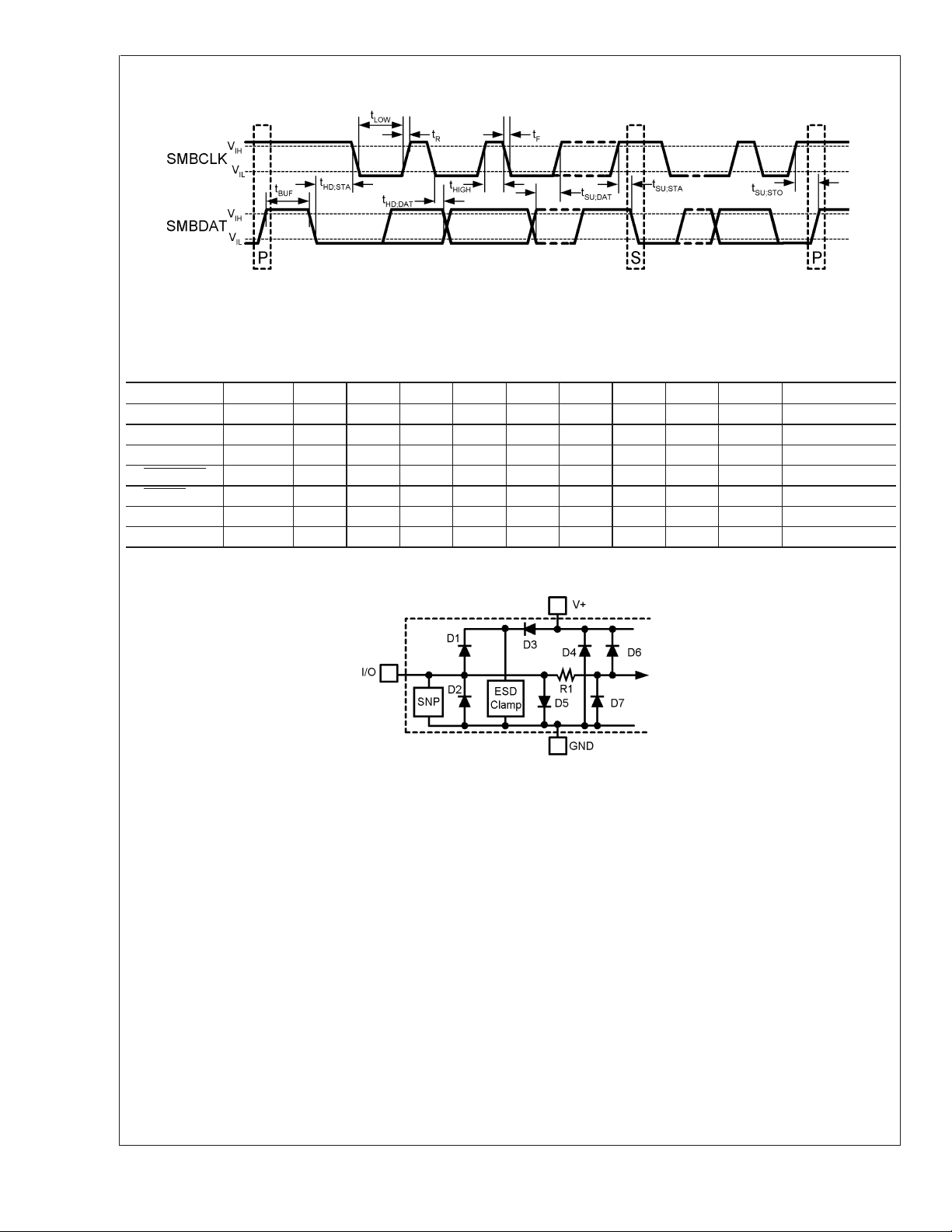
3.2 PCB LAYOUT FOR MINIMIZING NOISE
20053817
FIGURE 11. Ideal Diode Trace Layout
In a noisy environment, such as a processor mother board,
layout considerations are very critical. Noise induced on
traces running between the remote temperature diode sensor and the LM99 can cause temperature conversion errors.
Keep in mind that the signal level the LM99 is trying to
measure is in microvolts. The following guidelines should be
followed:
1. Place a 0.1 µF power supply bypass capacitor as close
as possible to the V
capacitor as close as possible to the LM99’s D+ and D−
pins. Make sure the traces to the 2.2 nF capacitor are
matched.
2. Ideally, the LM99 should be placed within 10 cm of the
Processor diode pins with the traces being as straight,
short and identical as possible. Trace resistance of 1 Ω
can cause as much as 1˚C of error. This error can be
compensated by using the Remote Temperature Offset
Registers, since the value placed in these registers will
automatically be subtracted from or added to the remote
temperature reading.
3. Diode traces should be surrounded by a GND guard ring
to either side, above and below if possible. This GND
pin and the recommended 2.2 nF
DD
LM99
guard should not be between the D+ and D− lines. In the
event that noise does couple to the diode lines it would
be ideal if it is coupled common mode. That is equally to
the D+ and D− lines.
4. Avoid routing diode traces in close proximity to power
supply switching or filtering inductors.
5. Avoid running diode traces close to or parallel to high
speed digital and bus lines. Diode traces should be kept
at least 2 cm apart from the high speed digital traces.
6. If it is necessary to cross high speed digital traces, the
diode traces and the high speed digital traces should
cross at a 90 degree angle.
7. The ideal place to connect the LM99’s GND pin is as
close as possible to the Processors GND associated
with the sense diode.
8. Leakage current between D+ and GND should be kept
to a minimum. One nano-ampere of leakage can cause
as much as 1˚C of error in the diode temperature reading. Keeping the printed circuit board as clean as possible will minimize leakage current.
Noise coupling into the digital lines greater than 400 mVp-p
(typical hysteresis) and undershoot less than 500 mV below
GND, may prevent successful SMBus communication with
the LM99. SMBus no acknowledge is the most common
symptom, causing unnecessary traffic on the bus. Although
the SMBus maximum frequency of communication is rather
low (100 kHz max), care still needs to be taken to ensure
proper termination within a system with multiple parts on the
bus and long printed circuit board traces. An RC lowpass
filter witha3dBcorner frequency of about 40 MHz is
included on the LM99’s SMBCLK input. Additional resistance
can be added in series with the SMBData and SMBCLK lines
to further help filter noise and ringing. Minimize noise coupling by keeping digital traces out of switching power supply
areas as well as ensuring that digital lines containing high
speed data communications cross at right angles to the
SMBData and SMBCLK lines.
www.national.com19
Page 20

Physical Dimensions inches (millimeters) unless otherwise noted
Interface
8-Lead Molded Mini-Small-Outline Package (MSOP),
JEDEC Registration Number MO-187
Order Number LM99CIMM or LM99CIMMX
NS Package Number MUA08A
LIFE SUPPORT POLICY
NATIONAL’S PRODUCTS ARE NOT AUTHORIZED FOR USE AS CRITICAL COMPONENTS IN LIFE SUPPORT
DEVICES OR SYSTEMS WITHOUT THE EXPRESS WRITTEN APPROVAL OF THE PRESIDENT AND GENERAL
COUNSEL OF NATIONAL SEMICONDUCTOR CORPORATION. As used herein:
2. A critical component is any component of a life
support device or system whose failure to perform
can be reasonably expected to cause the failure of
the life support device or system, or to affect its
safety or effectiveness.
1˚C Accurate, High Temperature, Remote Diode Temperature Sensor with Two-Wire
±
1. Life support devices or systems are devices or
systems which, (a) are intended for surgical implant
into the body, or (b) support or sustain life, and
whose failure to perform when properly used in
accordance with instructions for use provided in the
labeling, can be reasonably expected to result in a
significant injury to the user.
National Semiconductor
LM99
National does not assume any responsibility for use of any circuitry described, no circuit patent licenses are implied and National reserves the right at any time without notice to change said circuitry and specifications.
Americas Customer
Support Center
Email: new.feedback@nsc.com
Tel: 1-800-272-9959
www.national.com
National Semiconductor
Europe Customer Support Center
Fax: +49 (0) 180-530 85 86
Email: europe.support@nsc.com
Deutsch Tel: +49 (0) 69 9508 6208
English Tel: +44 (0) 870 24 0 2171
Français Tel: +33 (0) 1 41 91 8790
National Semiconductor
Asia Pacific Customer
Support Center
Email: ap.support@nsc.com
National Semiconductor
Japan Customer Support Center
Fax: 81-3-5639-7507
Email: jpn.feedback@nsc.com
Tel: 81-3-5639-7560
 Loading...