

Page 1
LM96000
Hardware Monitor with Integrated Fan Control
General Description
The LM96000, hardware monitor, has a two wire digital
interface compatible with SMBus 2.0. Using an 8-bit Σ∆
ADC, the LM96000 measures:
– the temperature of two remote diode connected transis-
tors as well as its own die
– the VCCP, 2.5V, 3.3VSBY, 5.0V, and 12V supplies (in-
ternal scaling resistors).
To set fan speed, the LM96000 has three PWM outputs that
are each controlled by one of three temperature zones. High
and low PWM frequency ranges are supported. The
LM96000 includes a digital filter that can be invoked to
smooth temperature readings for better control of fan speed.
The LM96000 has four tachometer inputs to measure fan
speed. Limit and status registers for all measured values are
included.
Features
n 2-wire, SMBus 2.0 compliant, serial digital interface
n 8-bit Σ∆ ADC
n Monitors VCCP, 2.5V, 3.3 VSBY, 5.0V, and 12V
motherboard/processor supplies
n Monitors 2 remote thermal diodes
n Programmable autonomous fan control based on
temperature readings
n Noise filtering of temperature reading for fan control
n 1.0˚C digital temperature sensor resolution
n 3 PWM fan speed control outputs
n Provides high and low PWM frequency ranges
n 4 fan tachometer inputs
n Monitors 5 VID control lines
n 24-pin TSSOP package
n XOR-tree test mode
Key Specifications
n Voltage Measurement Accuracy
n Resolution 8-bits, 1˚C
n Temperature Sensor Accuracy
n Temperature Range
— LM96000 Operational 0˚C to +85˚C
— Remote Temp Accuracy 0˚C to +125˚C
n Power Supply Voltage +3.0V to +3.6V
n Power Supply Current 0.53 mA
Applications
n Desktop PC
n Microprocessor based equipment
(e.g. Base-stations, Routers, ATMs, Point of Sales)
November 2004
±
2% FS (max)
±
3˚C (max)
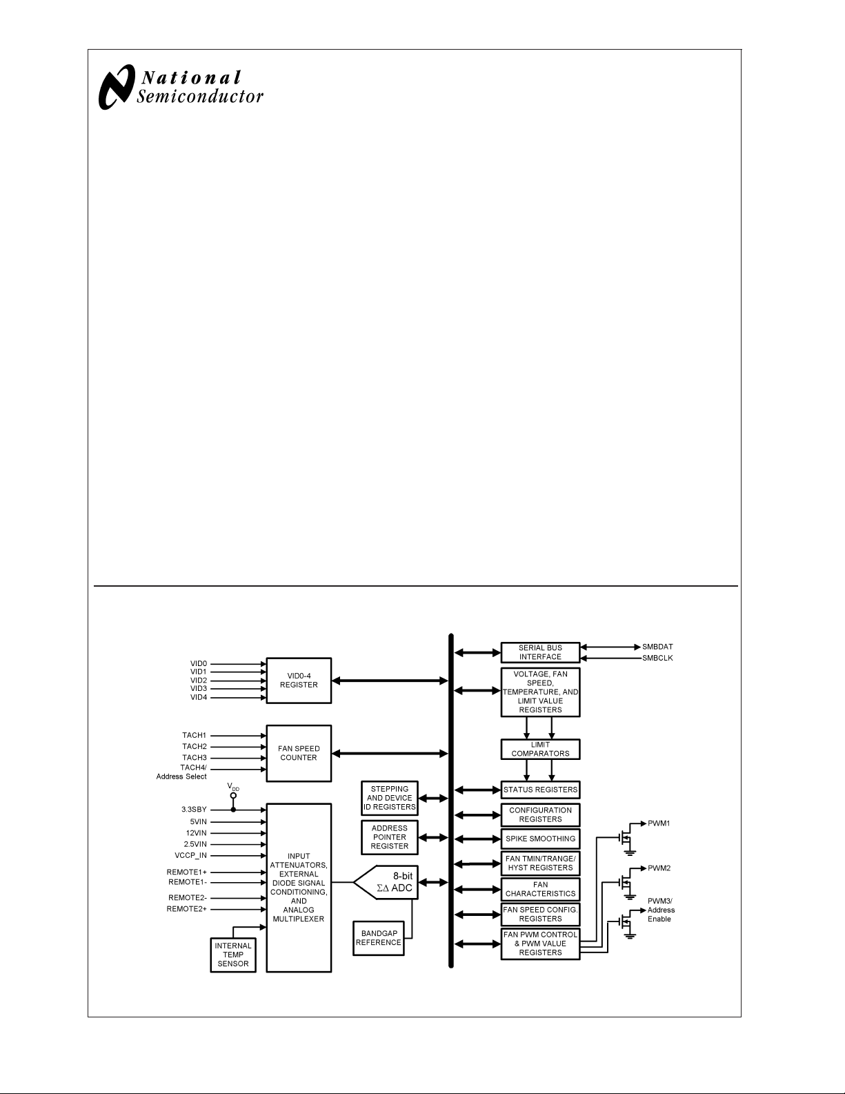
LM96000 Hardware Monitor with Integrated Fan Control
Block Diagram
20084601
© 2004 National Semiconductor Corporation DS200846 www.national.com
Page 2
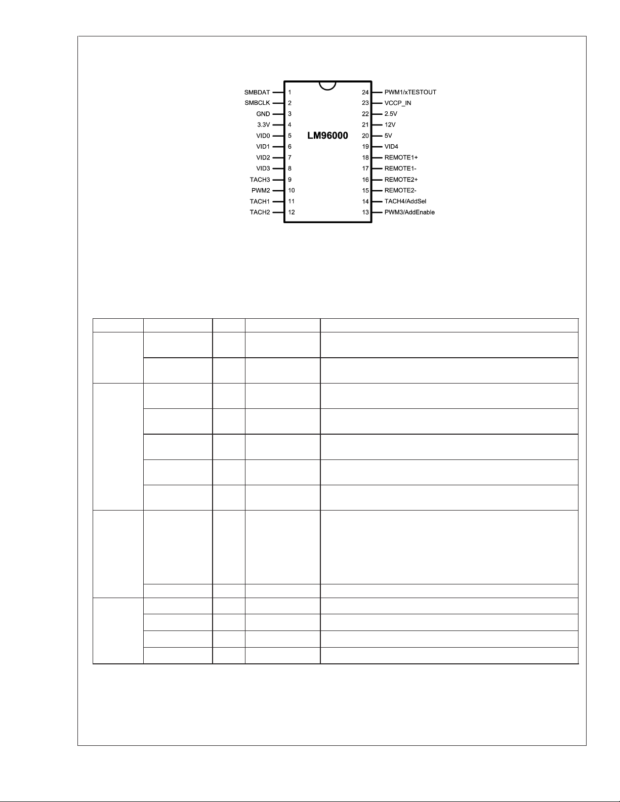
Connection Diagram
LM96000
Pin Descriptions
SMBus
Processor VID Lines
Power
Voltage Inputs
24 Pin TSSOP
NS Package MTC24E
Top View
LM96000CIMT (61 units per rail), or
LM96000CIMTX (2500 units per tape and reel)
Symbol Pin Type Name and Function/Connection
SMBDAT 1 Digital I/O
(Open-Drain)
SMBCLK 2 Digital Input System Management Bus Clock. Tied to Open-drain output. 5V
VID0 5 Digital Input Voltage identification signal from the processor. This value is read
VID1 6 Digital Input Voltage identification signal from the processor. This value is read
VID2 7 Digital Input Voltage identification signal from the processor. This value is read
VID3 8 Digital Input Voltage identification signal from the processor. This value is read
VID4 19 Digital Input Voltage identification signal from the processor. This value is read
3.3V 4 POWER +3.3V pin. Can be powered by +3.3V Standby power if monitoring
GND 3 GROUND Ground for all analog and digital circuitry.
5V 20 Analog Input Analog input for +5V monitoring.
12V 21 Analog Input Analog input for +12V monitoring.
2.5V 22 Analog Input Analog input for +2.5V monitoring.
VCCP_IN 23 Analog Input Analog input for VCCP (processor voltage) monitoring.
System Management Bus Data. Open-drain output. 5V tolerant,
SMBus 2.0 compliant.
tolerant, SMBus 2.0 compliant.
in the VID0–VID4 Status Register.
in the VID0–VID4 Status Register.
in the VID0–VID4 Status Register.
in the VID0–VID4 Status Register.
in the VID0–VID4 Status Register.
in low power states is required. This pin also serves as the analog
input to monitor the 3.3V supply. This pin should be bypassed
with a 0.1µf capacitor in parallel with 100pf. A bulk capacitance of
approximately 10µf needs to be in the near vicinity of the
LM96000.
20084602
www.national.com 2
Page 3
Pin Descriptions (Continued)
Symbol Pin Type Name and Function/Connection
Remote1+ 18 Remote Thermal
Remote1− 17 Remote Thermal
Remote
Remote2+ 16 Remote Thermal
Remote2− 15 Remote Thermal
TACH1 11 Digital Input Input for monitoring tachometer output of fan 1.
TACH2 12 Digital Input Input for monitoring tachometer output of fan 2.
TACH3 9 Digital Input Input for monitoring tachometer output of fan 3.
Diode Positive
Input
Diode Negative
Input
Diode Positive
Output
Diode Negative
Input
LM96000
Positive input (current source) from the first remote thermal diode.
Serves as the positive input into the A/D. Connected to
THERMDA pin of Pentium processor or the base of a diode
connected MMBT3904 NPN transistor.
Negative input (current sink) from the first remote thermal diode.
Serves as the negative input into the A/D. Connected to
THERMDC pin of Pentium processor or the emmiter of a diode
connected MMBT3904 NPN transistor.
Fan Tachometer Inputs
Fan Control
TACH4/Address
Select
PWM1/xTest
Out
PWM2 10 Digital Open-Drain
PWM3/Address
Enable
14 Digital Input Input for monitoring tachometer output of fan 4. If in Address
24 Digital Open-Drain
Output
Output
13 Digital Open-Drain
Output
Select Mode, determines the SMBus address of the LM96000.
Fan speed control 1. When in XOR tree test mode, functions as
XOR Tree output.
Fan speed control 2.
Fan speed control 3. Pull to ground at power on to enable
Address Select Mode (Address Select pin controls SMBus
address of the device).
www.national.com3
Page 4
Absolute Maximum Ratings (Notes 1, 2)
If Military/Aerospace specified devices are required,
LM96000
please contact the National Semiconductor Sales Office/
Distributors for availability and specifications.
Storage Temperature −65˚C to +150˚C
Soldering process must comply with National’s reflow
temperature profile specifications. Refer to
www.national.com/packaging/. (Note 6)
Supply Voltage, V+ −0.5V to 6.0V
Voltage on Any Digital Input or
−0.5V to 6.0V
Operating Ratings (Notes 1, 2)
Output Pin
Voltage on 12V Analog Input −0.5V to 16V
Voltage on 5V Analog Input −0.5V to 6.66V
Voltage on Remote1+, Remote2+, −0.5V to (V+ + 0.05V)
±
Current on Remote1−, Remote2−
1mA
Voltage on Other Analog Inputs −0.5V to 6.0V
Input Current on Any Pin (Note 3)
Package Input Current (Note 3)
Package Dissipation at T
= 25˚C See (Note 5)
A
±
5mA
±
20 mA
ESD Susceptibility (Note 4)
Human Body Model 2500V
Machine Model 250V
LM96000 Operating Temperature
Range
Remote Diode Temperature Range 0˚C ≤ T
Supply Voltage (3.3V nominal) +3.0V to +3.6V
V
Voltage Range
IN
+12V V
IN
+5V V
IN
+3.3V V
IN
VCCP_IN and All Other Inputs −0.05V to (V+ + 0.05V)
VID0–VID4 −0.05V to 5.5V
Typical Supply Current 0.53 mA
0˚C ≤ T
D
−0.05V to 16V
−0.05V to 6.66V
3.0V to 4.4V
DC Electrical Characteristics
The following specifications apply for V+ = 3.0V to 3.6V, and all analog input source impedance RS=50Ω unless otherwise
specified in conditions. Boldface limits apply for T
the ambient temperature of the LM96000; T
is the junction temperature of the LM96000; TDis the thermal diode junction tem-
J
A=TJ
over T
perature.
Symbol Parameter Conditions Typical
POWER SUPPLY CHARACTERISTICS
Supply Current (Note 9) Converting, Interface and
Power-On Reset Threshold Voltage 1.6 V (min)
TEMPERATURE TO DIGITAL CONVERTER CHARACTERISTICS
Resolution 1
Temperature Accuracy (See (Note 10) for Thermal
Diode Processor Type)
Temperature Accuracy using Internal Diode (Note
11)
I
DS
External Diode Current Source High Level 188 280 µA (max)
External Diode Current Ratio 16
ANALOG TO DIGITAL CONVERTER CHARACTERISTICS
TUE Total Unadjusted Error(Note 12)
DNL Differential Non-linearity 1 LSB
Power Supply Sensitivity
Total Monitoring Cycle Time (Note 13) All Voltage and
MIN
=0˚C to T
=85˚C; all other limits TA=TJ= 25˚C. TAis
MAX
Limits
(Note 7)
(Note 8)
1.8 3.5 mA (max)
Fans Inactive, Peak
Current
Converting, Interface and
0.53 mA
Fans Inactive, Average
Current
2.8 V (max)
8
=25˚C
T
D
T
=0˚C to 100˚C
D
T
=100˚C to 125˚C
D
±
1
±
1
±
2.5 ˚C (max)
±
3 ˚C (max)
±
4 ˚C (max)
±
3 ˚C (max)
Low Level 11.75 µA
±
2 %FS (max)
±
1 %/V
182 200 ms (max)
Temperature readings
≤ +85˚C
A
≤ +125˚C
Units
(Limits)
˚C
Bits
www.national.com 4
Page 5
DC Electrical Characteristics (Continued)
The following specifications apply for V+ = 3.0V to 3.6V, and all analog input source impedance RS=50Ω unless otherwise
specified in conditions. Boldface limits apply for T
the ambient temperature of the LM96000; T
is the junction temperature of the LM96000; TDis the thermal diode junction tem-
J
A=TJ
over T
perature.
Symbol Parameter Conditions Typical
Input Resistance, all analog inputs 210 140 kΩ (min)
DIGITAL OUTPUT: PWM1, PWM2, PWM3, XTESTOUT
I
OL
V
OL
Logic Low Sink Current VOL=0.4V 8 mA (min)
Logic Low Level I
SMBUS OPEN-DRAIN OUTPUT: SMBDAT
V
OL
I
OH
Logic Low Output Voltage I
High Level Output Current V
SMBUS INPUTS: SMBCLK. SMBDAT
V
V
V
IH
IL
HYST
Logic Input High Voltage 2.1 V (min)
Logic Input Low Voltage 0.8 V (max)
Logic Input Hysteresis Voltage 300 mV
DIGITAL INPUTS: ALL
V
IH
V
IL
V
TH
I
IH
I
IL
C
IN
Logic Input High Voltage 2.1 V (min)
Logic Input Low Voltage 0.8 V (max)
Logic Input Threshold Voltage 1.5 V
Logic High Input Current VIN= V+ 0.005 10 µA (max)
Logic Low Input Current VIN= GND −0.005 −10 µA (max)
Digital Input Capacitance 20 pF
MIN
=0˚C to T
=85˚C; all other limits TA=TJ= 25˚C. TAis
MAX
Limits
(Note 7)
(Note 8)
400 kΩ (max)
=+8mA 0.4 V (max)
OUT
=+4mA 0.4V V (max)
OUT
= V+ 0.1 10 µA (max)
OUT
LM96000
Units
(Limits)
AC Electrical Characteristics
The following specifications apply for V+ = 3.0V to 3.6V unless otherwise specified in conditions. Boldface limits apply for T
=TJover T
Symbol Parameter Conditions Typical
TACHOMETER ACCURACY
FAN PWM OUTPUT
SPIKE SMOOTHING FILTER
SMBUS TIMING CHARACTERISTICS
f
SMB
MIN
=0˚C to T
=85˚C; all other limits TA=TJ= 25˚C.
MAX
Limits
(Note 7)
Fan Count Accuracy
(Note 8)
±
10 % (max)
(Limits)
Fan Full-Scale Count 65536 (max)
Fan Counter Clock Frequency 90 kHz
Fan Count Conversion Time 0.7 1.4 sec (max)
Frequency Setting Accuracy
±
10 % (max)
Frequency Range 10
30
Duty-Cycle Range Low frequency range 0to100 % (max)
Duty-Cycle Resolution (8-bits) 0.390625 %
Spin-Up Time Interval Range 100
4000
Spin-Up Time Interval Accuracy
Time Interval Deviation
±
10 % (max)
±
10 % (max)
Time Interval Range 35
0.8
SMBus Operating Frequency 10
100
kHz (min)
kHz (max)
A
Units
Hz
kHz
ms ms
sec
sec
www.national.com5
Page 6
AC Electrical Characteristics (Continued)
The following specifications apply for V+ = 3.0V to 3.6V unless otherwise specified in conditions. Boldface limits apply for T
=TJover T
LM96000
Symbol Parameter Conditions Typical
f
BUF
t
HD_STA
t
SU:STA
t
SU:STO
t
HD:DAT
t
SU:DAT
t
TIMEOUT
t
LOW
t
HIGH
t
F
t
R
t
POR
MIN
=0˚C to T
=85˚C; all other limits TA=TJ= 25˚C.
MAX
Limits
(Note 7)
SMBus Free Time Between Stop And
(Note 8)
4.7 µs (min)
Start Condition
Hold Time After (Repeated) Start
4.0 µs (min)
Condition (after this period, the first
clock is generated)
Repeated Start Condition Setup Time 4.7 µs (min)
Stop Condition Setup Time 4.0 µs (min)
Data Output Hold Time 300 ns (min)
930 ns (max)
Data Input Setup Time 250 ns (min)
Data And Clock Low Time To Reset
Of SMBus Interface Logic(Note 14)
25
35
Clock Low Period 4.7 µs (min)
Clock High Period 4.0
50
Clock/Data Fall Time 300 ns (max)
Clock/Data Rise Time 1000 ns (max)
Time from Power-On-Reset to
V+>2.8V 500 ms (max)
LM96000 Reset and Operational
A
Units
(Limits)
ms (min)
ms (max)
µs (min)
µs (max)
20084603
Note 1: Absolute Maximum Ratings indicate limits beyond which damage to the device may occur. Operating Ratings indicate conditions for which the device is
functional, but do not guarantee specific performance limits. For guaranteed specifications and test conditions, see the Electrical Characteristics. The guaranteed
specifications apply only for the test conditions listed. Some performance characteristics may degrade when the device is not operated under the listed test
conditions.
Note 2: All voltages are measured with respect to GND, unless otherwise noted.
Note 3: When the input voltage (V
maximum package input current rating limits the number of pins that can safely exceed the power supplies with an input current of 5mAto four. Parasitic components
and/or ESD protection circuitry are shown below for the LM96000’s pins. The nominal breakdown voltage the zener is 6.5V. Care should be taken not to forward bias
the parasitic diode D1 present on pins D+ and D−. Doing so by more that 50 mV may corrupt temperature measurements. SNP stands for snap-back device.
www.national.com 6
) at any pin exceeds the power supplies (V
IN
IN
<
GND or V
>
V+ ), the current at that pin should be limited to 5mA. The 20mA
IN
Page 7
LM96000
Pin
#
Pin
Name Circuit All Input Circuits
1 SMBDAT A
2 SMBCLK
3 GND B
4 3.3V
5 VID0 A
6 VID1
7 VID2
8 VID3
9 TACH3
10 PWM2
11 TACH1
12 TACH2
13 PWM3/AddEnable
14 TACH4/AddSel
15 REMOTE2− C
Circuit A
Circuit B
Circuit C
16 REMOTE2+ D
17 REMOTE1− C
18 REMOTE1+ D
19 VID4 A
Circuit D
20 5V E
21 12V
22 2.5V
23 VCCP_IN
24 PWM1/xTEXTOUT A
Circuit E
Note 4: Human body model, 100pF discharged through a 1.5kΩ resistor. Machine model, 200pF discharged directly into each pin.
Note 5: Thermal resistance junction-to-ambient when attached to a double-sided printed circuit board with 1 oz. foil is 113 ˚C/W.
Note 6: Reflow temperature profiles are different for packages containing lead (Pb) than for those that do not.
Note 7: Typicals are at T
Note 8: Limits are guaranteed to National’s AOQL (Average Outgoing Quality Level).
Note 9: The average current can be calculated from the peak current using the following equation:
Quiescent current will not increase substantially with an SMBus transaction.
Note 10: The accuracy of the LM96000CIMT is guaranteed when using the thermal diode of Intel Pentium 4 90nm processors or any thermal diode with a
non-ideality of 1.011 and series resistance of 3.33Ω. When using a 2N3904 type transistor as a thermal diode the error band will be typically shifted by -?˚C.
Note 11: Local temperature accuracy does not include the effects of self-heating. The rise in temperature due to self-heating is the product of the internal power
dissipation of the LM96000 and the thermal resistance. See (Note 5) for the thermal resistance to be used in the self-heating calculation.
Note 12: TUE , total unadjusted error, includes ADC gain, offset, linearity and reference errors. TUE is defined as the "actual Vin" to achieve a given code transition
minus the "theoretical Vin" for the same code. Therefore, a positive error indicates that the input voltage is greater than the theoretical input voltage for a given code.
If the theoretical input voltage was applied to an LM96000 that has positive error, the LM96000’s reading would be less than the theoretical.
Note 13: This specification is provided only to indicate how often temperature and voltage data is updated. The LM96000 can be read at any time without regard
to conversion state (and will yield last conversion result).
= 25˚C and represent most likely parametric norm.
A
www.national.com7
Page 8
Note 14: Holding the SMBDAT and/or SMBCLK lines Low for a time interval greater than t
the SMBDAT pin to a high impedance state.
LM96000
Functional Description
will reset the LM96000’s SMBus state machine, therefore setting
TIMEOUT
1.0 SMBUS
The LM96000 is compatible with devices that are compliant to the SMBus 2.0 specification. More information on this bus can be
found at: http://www.smbus.org/. Compatibility of SMBus2.0 to other buses is discussed in the SMBus 2.0 specification.
1.1 Addressing
LM96000 is designed to be used primarily in desktop systems that require only one monitoring device.
If only one LM96000 is used on the motherboard, the designer should be sure that the Address Enable/PWM3 pin is High during
the first SMBus communication addressing the LM96000. Address Enable/PWM3 is an open drain I/O pin that at power-on
defaults to the input state of Address Enable. A maximum of 10k pull-up resistance on Address Enable/PWM3 is required to
assure that the SMBus address of the device will be locked at 010 1110b, which is the default address of the LM96000.
During the first SMBus communication TACH4 and PWM3 can be used to change the SMBus address of the LM96000 to
0101101b or 0101100b. LM96000 address selection procedure:
A10kΩ pull-down resistor to ground on the Address Enable/PWM3 pin is required. Upon power up, the LM96000 will be placed
into Address Enable mode and assign itself an SMBus address according to the state of the Address Select input. The
LM96000 will latch the address during the first valid SMBus transaction in which the first five bits of the targeted address match
those of the LM96000 address, 0 1011b. This feature eliminates the possibility of a glitch on the SMBus interfering with address
selection. When the PWM3/Address Enable pin is not used to change the SMBus address of the LM96000, it will remain in a
high state until the first communication with the LM96000. After the first SMBus transaction is completed PWM3 and TACH4 will
return to normal operation.
Address Enable Address Select Board Implementation SMBus Address
0 0 Pulled to ground through a 10 kΩ resistor 010 1100b, 2Ch
0 1 Pulled to 3.3V or to GND through a 10 kΩ resistor 010 1101b, 2Dh
1 X Pulled to 3.3V through a 10 kΩ resistor 010 1110b, 2Eh
In this way, up to three LM96000 devices can exists on an SMBus at any time. Multiple LM96000 devices can be used to monitor
additional processors and temperature zones. When using the non-default addresses additional circuitry will be required if TACH4
and PWM3 require to function correctly. Such circuitry could consist of GPIO pins from a micro-controller. During the first
communication the micro-controller would drive the Address Enable and Address Select pins to the proper state for the required
address. After the first SMBus communication the micro-controller would drive it’s pins into TRISTATE allowing TACH4 and
PWM3 to operate correctly.
20084604
2.0 FAN REGISTER DEVICE SET-UP
The BIOS will follow the following steps to configure the fan registers on the LM96000. The registers corresponding to each
function are listed. All steps may not be necessary if default values are acceptable. Regardless of all changes made by the BIOS
to the fan limit and parameter registers during configuration, the LM96000 will continue to operate based on default values until
the START bit (bit 0), in the Ready/Lock/Start/Override register (address 40h), is set. Once the fan mode is updated, by setting
the START bit to 1, the LM96000 will operate using the values that were set by the BIOS in the fan control limit and parameter
registers (adress 5Ch through 6Eh).
www.national.com 8
Page 9

Functional Description (Continued)
1. Set limits and parameters (not necessarily in this order):
– [5F-61h] Set PWM frequencies and auto fan control range.
– [62-63h] Set spike smoothing and min/off.
– [5C-5Eh] Set the fan spin-up delays.
– [5C-5Eh] Match each fan with a corresponding thermal zone.
– [67-69h] Set the fan temperature limits.
– [6A-6Ch] Set the temperature absolute limits.
– [64-66h] Set the PWM minimum duty cycle.
– [6D-6Eh] Set the temperature Hysteresis values.
2. [40h] Set bit 0 (START) to update fan control and limit register values and start fan control based on these new values.
3. [40h] Set bit 1 (LOCK) to lock the fan limit and parameter registers (optional).
3.0 AUTO FAN CONTROL OPERATING MODE
The LM96000 includes the circuitry for automatic fan control. In Auto Fan Mode, the LM96000 will automatically adjust the PWM
duty cycle of the PWM outputs. PWM outputs are assigned to a thermal zone based on the fan configuration registers. It is
possible to have more than one PWM output assigned to a thermal zone. For example, PWM outputs 2 and 3, connected to two
chassis fans, may both be controlled by thermal zone 2. At any time, the temperature of a zone exceeds its absolute limit, all PWM
outputs will go to 100% duty cycle to provide maximum cooling to the system.
4.0 REGISTER SET
LM96000
Register
Address
20h R 2.5V 7 6 5 4 3 2 1 0 N/A
21h R VCCP_IN 7 6 5 4 3 2 1 0 N/A
22h R 3.3V 7 6 5 4 3 2 1 0 N/A
23h R 5V 7 6 5 4 3 2 1 0 N/A
24h R 12V 7 6 5 4 3 2 1 0 N/A
25h R Processor (Zone1) Temp 7 6 5 4 3 2 1 0 N/A
26h R Internal (Zone2) Temp 7 6 5 4 3 2 1 0 N/A
27h R Remote (Zone3) Temp 7 6 5 4 3 2 1 0 N/A
28h R Tach1 LSB 7 6 5 4 3 2 LEVEL1 LEVEL0 N/A
29h R Tach1 MSB 15 14 13 12 11 10 9 8 N/A
2Ah R Tach2 LSB 7 6 5 4 3 2 LEVEL1 LEVEL0 N/A
2Bh R Tach2 MSB 15 14 13 12 11 10 9 8 N/A
2Ch R Tach3 LSB 7 6 5 4 3 2 LEVEL1 LEVEL0 N/A
2Dh R Tach3 MSB 15 14 13 12 11 10 9 8 N/A
2Eh R Tach4 LSB 7 6 5 4 3 2 LEVEL1 LEVEL0 N/A
2Fh R Tach4 MSB 15 14 13 12 11 10 9 8 N/A
30h R/W Fan1 Current PWM Duty 7 6 5 4 3 2 1 0 N/A
31h R/W Fan2 Current PWM Duty 7 6 5 4 3 2 1 0 N/A
32h R/W Fan3 Current PWM Duty 7 6 5 4 3 2 1 0 N/A
3Eh R Company ID 7 6 5 4 3 2 1 0 01h
3Fh R Version/Stepping VER3 VER2 VER1 VER0 STP3 STP2 STP1 STP0 68h
40h R/W Ready/Lock/Start/Override RES RES RES RES OVRID READY LOCK START 00h
41h R Interrupt Status Register 1 ERR ZN3 ZN2 ZN1 5V 3.3V VCCP 2.5V 00h
42h R Interrupt Status Register 2 ERR2 ERR1 FAN4 FAN3 FAN2 FAN1 RES 12V 00h
43h R VID0–4 RES RES RES VID4 VID3 VID2 VID1 VID0 N/A
44h R/W 2.5V Low Limit 7 6 5 4 3 2 1 0 00h
45h R/W 2.5V High Limit 7 6 5 4 3 2 1 0 FFh
46h R/W VCCP Low Limit 7 6 5 4 3 2 1 0 00h
47h R/W VCCP High Limit 7 6 5 4 3 2 1 0 FFh
48h R/W 3.3V Low Limit 7 6 5 4 3 2 1 0 00h
Read/
Write
Register
Name
Bit 7
(MSB)
Bit 6 Bit 5 Bit 4 Bit 3 Bit 2 Bit 1 Bit 0
(LSB)
Default
Value
Lock?
www.national.com9
Page 10

Functional Description (Continued)
Register
LM96000
Address
49h R/W 3.3V High Limit 7 6 5 4 3 2 1 0 FFh
4Ah R/W 5V Low Limit 7 6 5 4 3 2 1 0 00h
4Bh R/W 5V High Limit 7 6 5 4 3 2 1 0 FFh
4Ch R/W 12V Low Limit 7 6 5 4 3 2 1 0 00h
4Dh R/W 12V High Limit 7 6 5 4 3 2 1 0 FFh
4Eh R/W Processor (Zone1) Low
4Fh R/W Processor (Zone1) High
50h R/W Internal (Zone2) Low
51h R/W Internal (Zone2) High
52h R/W Remote (Zone3) Low
53h R/W Remote (Zone3) High
54h R/W Tach1 Minimum LSB 7 6 5 4 3 2 1 0 FFh
55h R/W Tach1 Minimum MSB 15 14 13 12 11 10 9 8 FFh
56h R/W Tach2 Minimum LSB 7 6 5 4 3 2 1 0 FFh
57h R/W Tach2 Minimum MSB 15 14 13 12 11 10 9 8 FFh
58h R/W Tach3 Minimum LSB 7 6 5 4 3 2 1 0 FFh
59h R/W Tach3 Minimum MSB 15 14 13 12 11 10 9 8 FFh
5Ah R/W Tach4 Minimum LSB 7 6 5 4 3 2 1 0 FFh
5Bh R/W Tach4 Minimum MSB 15 14 13 12 11 10 9 8 FFh
5Ch R/W Fan1 Configuration ZON2 ZON1 ZON0 INV RES SPIN2 SPIN1 SPIN0 62h U
5Dh R/W Fan2 Configuration ZON2 ZON1 ZON0 INV RES SPIN2 SPIN1 SPIN0 62h U
5Eh R/W Fan3 Configuration ZON2 ZON1 ZON0 INV RES SPIN2 SPIN1 SPIN0 62h U
5Fh R/W Fan1 Range/Frequency RAN3 RAN2 RAN1 RAN0 HLFRQ FRQ2 FRQ1 FRQ0 C4h U
60h R/W Fan2 Range/Frequency RAN3 RAN2 RAN1 RAN0 HLFRQ FRQ2 FRQ1 FRQ0 C4h U
61h R/W Fan3 Range/Frequency RAN3 RAN2 RAN1 RAN0 HLFRQ FRQ2 FRQ1 FRQ0 C4h U
62h R/W Min/Off, Zone1 Spike
63h R/W Zone2, Zone3 Spike
64h R/W Fan1 PWM Minimum 7 6 5 4 3 2 1 0 80h U
65h R/W Fan2 PWM Minimum 7 6 5 4 3 2 1 0 80h U
66h R/W Fan3 PWM Minimum 7 6 5 4 3 2 1 0 80h U
67h R/W Zone1 Fan Temp Limit 7 6 5 4 3 2 1 0 5Ah U
68h R/W Zone2 Fan Temp Limit 7 6 5 4 3 2 1 0 5Ah U
69h R/W Zone3 Fan Temp Limit 7 6 5 4 3 2 1 0 5Ah U
6Ah R/W Zone1 Temp Absolute
6Bh R/W Zone2 Temp Absolute
6Ch R/W Zone3 Temp Absolute
6Dh R/W Zone1, Zone2 Hysteresis H1-3 H1-2 H1-1 H1-0 H2-3 H2-2 H2-1 H2-0 44h U
6Eh R/W Zone3 Hysteresis H3-3 H3-2 H3-1 H3-0 RES RES RES RES 40h U
Read/
Write
Register
Name
Temp
Temp
Temp
Temp
Temp
Temp
Smoothing
Smoothing
Limit
Limit
Limit
Bit 7
(MSB)
OFF3 OFF2 OFF1 RES ZN1E ZN1-2 ZN1-1 ZN1-0 00H U
ZN2E ZN2-2 ZN2-1 ZN2-0 ZN3E ZN3-2 ZN3-1 ZN3-0 00h U
Bit 6 Bit 5 Bit 4 Bit 3 Bit 2 Bit 1 Bit 0
(LSB)
7 6 5 4 3 2 1 0 81h
7 6 5 4 3 2 1 0 7Fh
7 6 5 4 3 2 1 0 81h
7 6 5 4 3 2 1 0 7Fh
7 6 5 4 3 2 1 0 81h
7 6 5 4 3 2 1 0 7Fh
7 6 5 4 3 2 1 0 64h U
7 6 5 4 3 2 1 0 64h U
7 6 5 4 3 2 1 0 64h U
Default
Value
Lock?
www.national.com 10
Page 11

Functional Description (Continued)
LM96000
Register
Address
6Fh R/W XOR Test Tree Enable RES RES RES RES RES RES RES XEN 00h U
74h R/W Tach Monitor Mode RES RES T3/4-1 T3/4-0 T2-1 T2-0 T1-1 T1-0 00h
75h R/W Fan Spin-up Mode RES RES RES RES RES PWM3SUPWM2SUPWM1SU7h U
Note: Reserved bits will always return 0 when read.
4.1 Register 20-24h: Voltage Reading
Register
Address
20h R 2.5V 7 6543210 N/A
21h R VCCP 7 6543210 N/A
22h R 3.3V 7 6543210 N/A
23h R 5V 7 6543210 N/A
24h R 12V 7 6543210 N/A
The Register Names difine the typical input voltage at which the reading is
The Voltage Reading registers are updated automatically by the LM96000 at a minimum frequency of 4 Hz. These registers are
read only — a write to these registers has no effect.
4.2 Register 25-27h: Temperature Reading
Register
Address
25h R Processor (Zone1) Temp 7 6543210 N/A
26h R Internal (Zone2) Temp 7 6543210 N/A
27h R Remote (Zone3) Temp 7 6543210 N/A
Read/
Write
Read/
Write
Register
Name
Read/
Write
Register
Name
Register
Name
Bit 7
(MSB)
Bit 7
Bit 6 Bit 5 Bit 4 Bit 3 Bit 2 Bit 1 Bit 0
(MSB)
Bit 6 Bit 5 Bit 4 Bit 3 Bit 2 Bit 1 Bit 0
3
⁄4full scale or C0h.
Bit 7
(MSB)
Bit 6 Bit 5 Bit 4 Bit 3 Bit 2 Bit 1 Bit 0
(LSB)
(LSB)
(LSB)
Default
Value
Lock?
Default
Value
Default
Value
The Temperature Reading registers reflect the current temperatures of the internal and remote diodes. Processor (Zone1) Temp
register reports the temperature measured by the thermal diode connected to the Remote1− and Remote1+ pins, Remote
(Zone3) Temp register reports the temperature measured by the thermal diode connected to the the Remote2− and Remote2+
pins, and the Internal (Zone2) Temp register reports the temperature measured by the internal (junction) temperature sensor.
Temperatures are represented as 8 bit, 2’s complement, signed numbers, in Celsius, as shown below in Table 1. The Temperature
Reading register will return a value of 80h if the remote diode pins are not used by the board designer or are not functioning
properly. This reading will cause the zone limit bit(s) (bits 6 and 4) in the Interrupt Status Register (41h) and the remote diode fault
status bit(s) (bit 6 or 7) in the Interrupt Status Register 2 (42h) to be set. The Temperature Reading registers are updated
automatically by the LM96000 at a minimum frequency of 4 Hz. These registers are read only — a write to these registers has
no effect.
TABLE 1. Temperature vs Register Reading
Temperature Reading (Dec) Reading (Hex)
−127˚C −127 81h
.
.
.
−50˚C −50 CEh
.
.
.
.
.
.
www.national.com11
Page 12

Functional Description (Continued)
LM96000
4.3 Register 28-2Fh: Fan Tachometer Reading
TABLE 1. Temperature vs Register Reading (Continued)
Temperature Reading (Dec) Reading (Hex)
(SENSOR ERROR) 80h
.
.
.
0˚C 0 00h
.
.
.
127˚C 127 7Fh
.
.
.
.
.
.
.
.
.
.
.
.
Register
Address
28h
29h
2Ah
2Bh
2Ch
2Dh
2Eh
2Fh
The Fan Tachometer Reading registers contain the number of 11.111 µs periods (90 kHz) between full fan revolutions. The results
are based on the time interval of two tachometer pulses, since most fans produce two tachometer pulses per full revolution. These
registers will be updated at least once every second.
The value, for each fan, is represented by a 16-bit unsigned number.
The Fan Tachometer Reading registers will always return an accurate fan tachometer measurement, even when a fan is disabled
or non-functional.
The least two significant bits (LEVEL1 and LEVEL2) of the least significant byte are used to indicate the accuracy level of the
tachometer reading. The accuracy ranges from most to least accurate. [LEVEL1:LEVEL2]=11indicates a most accurate value,
[LEVEL1:LEVEL2]=01 indicates the least accurate value and [LEVEL1:LEVEL2]=00 is reserved for future use.
FF FFh indicates that the fan is not spinning, or that the tachometer input is not connected to a valid signal. These registers are
read only — a write to these registers has no effect.
When the LSByte of the LM96000 16-bit register is read, the other byte (MSByte) is latched at the current value until it is read.
At the end of the MSByte read the Fan Tachometer Reading registers are updated.
During spin-up, the PWM duty cycle reported is 0%.
Read/
Write
R
R
R
R
R
R
R
R
Register
Name
Tach1 LSB
Tach1 MSB715
Tach2 LSB
Tach2 MSB715
Tach3 LSB
Tach3 MSB715
Tach4 LSB
Tach4 MSB715
Bit 7
(MSB)
Bit 6 Bit 5 Bit 4 Bit 3 Bit 2 Bit 1 Bit 0
(LSB)
6
14
6
14
6
14
6
14
5
13
5
13
5
13
5
13
4
12
4
12
4
12
4
12
3
11
3
11
3
11
3
11
2
10
2
10
2
10
2
10
LEVEL19LEVEL08N/A
LEVEL19LEVEL08N/A
LEVEL19LEVEL08N/A
LEVEL19LEVEL08N/A
Default
Value
N/A
N/A
N/A
N/A
4.4 Register 30-32h: Current PWM Duty
Register
Address
30h R/W Fan1 Current PWM Duty 7 6543210 N/A
31h R/W Fan2 Current PWM Duty 7 6543210 N/A
32h R/W Fan3 Current PWM Duty 7 6543210 N/A
The Current PWM Duty registers store the current duty cycle at each PWM output. At initial power-on, the PWM duty cycle is
100% and thus, when read, this register will return FFh. After the Ready/Lock/Start/Override register Start bit is set, this register
and the PWM signals will be updated based on the algorithm described in the Auto Fan Control Operating Mode section.
When read, the Current PWM Duty registers return the current PWM duty cycle. These registers are read only unless the fan is
in manual (test) mode, in which case a write to these registers will directly control the PWM duty cycle for each fan. The PWM
duty cycle is represented as shown in the following table.
www.national.com 12
Read/
Write
Register
Name
Bit 7
(MSB)
Current Duty Value (Decimal) Value (Hex)
0% 0 00h
Bit 6 Bit 5 Bit 4 Bit 3 Bit 2 Bit 1 Bit 0
(LSB)
Default
Value
Page 13

Functional Description (Continued)
Current Duty Value (Decimal) Value (Hex)
0.3922% 1 01h
.
.
.
25.098% 64 40h
.
.
.
50.196% 128 80h
.
.
.
100% 255 FFh
4.5 Register 3Eh: Company ID
LM96000
.
.
.
.
.
.
.
.
.
.
.
.
.
.
.
.
.
.
Register
Address
3Eh R Company ID 7 6543210 01h
The company ID register contains the company identification number. For National Semiconductor this is 01h. This number is
assigned by Intel and is a method for uniquely identifying the part manufacturer. This register is read only — a write to this
register has no effect.
4.6 Register 3Fh: Version/Stepping
Register
Address
3Fh R Version/Stepping VER3 VER2 VER1 VER0 STP3 STP2 STP1 STP0 68h
The four least significant bits of the Version/Stepping register [3.0] contain the current stepping of the LM96000 silicon. The four
most significant bits [7.4] reflect the LM96000 base device number when set to a value of 0110b. For the LM96000, this register
will read 01101000b (68h). Bit 3 of the stepping field is set to indicate that the LM96000 is a super-set of the LM85 family of
products.
The register is used by application software to identify which device in the hardware monitor family of ASICs has been
implemented in the given system. Based on this information, software can determine which registers to read from and write to.
Further, application software may use the current stepping to implement work-arounds for bugs found in a specific silicon
stepping.
This register is read only — a write to this register has no effect.
4.7 Register 40h: Ready/Lock/Start/Override
Register
Address
40h R/W Ready/Lock/Start/Override RES RES RES RES OVRID READY LOCK START 00h
Read/
Write
Read/
Write
Read/
Write
Register
Name
Register
Name
Register
Name
Bit 7
(MSB)
Bit 7
(MSB)
Bit 6 Bit 5 Bit 4 Bit 3 Bit 2 Bit 1 Bit 0
Bit 6 Bit 5 Bit 4 Bit 3 Bit 2 Bit 1 Bit 0
Bit 7
(MSB)
Bit 6 Bit 5 Bit 4 Bit 3 Bit 2 Bit 1 Bit 0
(LSB)
(LSB)
(LSB)
Default
Value
Default
Value
Default
Value
www.national.com13
Page 14

Functional Description (Continued)
Bit Name R/W Default Description
LM96000
0 START R/W 0 When software writesa1tothis bit, the LM96000 fan monitoring and PWM
output control functions will use the values set in the fan control limit and
parameter registers (address 5Ch through 6Eh). Before this bit is set, the
LM96000 will not update the used register values, the default values will
remain in effect. Whenever this bit is set to 0, the LM96000 fan monitoring and
PWM output control functions use the default fan limits and parameters,
regardless of the current values in the limit and parameter registers (5C
through 6Eh). The LM96000 will preserve the values currently stored in the
limit and parameter registers when this bit is set or cleared. This bit is not
effected by the state of the Lock bit.
It is expected that all limit and parameter registers will be set by BIOS or
application software prior to setting this bit.
1 LOCK R/W 0 Setting this bit to 1 locks specified limit and parameter registers. Once this bit
is set, limit and parameter registers become read only and will remain locked
until the device is powered off. This register bit becomes read only once it is
set.
2 READY R 0 The LM96000 sets this bit automatically after the part is fully powered up, has
completed the power-up-reset process, and after all A/D converters are
properly functioning.
3 OVRID R/W If this bit is set to 1, all PWM outputs will go to 100% duty cycle regardless of
whether or not the lock bit is set. The OVRID bit has precedence over the
disabled mode. Therefore, when OVRID is set the PWM will go to 100% even
if the PWM is in the disabled mode.
4–7 Reserved R 0 Reserved
4.8 Register 41h: Interrupt Status Register 1
Register
Address
41h R Interrupt Status 1 ERR ZN3 ZN2 ZN1 5V 3.3V VCCP 2.5V 00h
The Interrupt Status Register 1 bits will be automatically set, by the LM96000, whenever a fault condition is detected. A fault
condition is detected whenever a measured value is outside the window set by its limit registers. ZN3 and ZN1 bits will be set
when a diode fault condition, such as a disconect or short, is detected. More than one fault may be indicated in the interrupt
register when read. This register will hold a set bit(s) until the event is read by software. The contents of this register will be
cleared (set to 0) automatically by the LM96000 after it is read by software, if the fault condition is no longer exists. Once set, the
Interrupt Status Register 1 bits will remain set until a read event occurs, even if the fault condition no longer exists
This register is read only — a write to this register has no effect.
Bit Name R/W Default Description
0 2.5V_Error R 0 The LM96000 automatically sets this bit to 1 when the 2.5V input voltage
1 VCCP_Error R 0 The LM96000 automatically sets this bit to 1 when the VCCP input voltage
2 3.3V_Error R 0 The LM96000 automatically sets this bit to 1 when the 3.3V input voltage
3 5V_Error R 0 The LM96000 automatically sets this bit to 1 when the 5V input voltage is
Read/
Write
Register
Name
Bit 7
(MSB)
Bit 6 Bit 5 Bit 4 Bit 3 Bit 2 Bit 1 Bit 0
(LSB)
is less than or equal to the limit set in the 2.5V Low Limit register or
greater than the limit set in the 2.5V High Limit register.
is less than or equal to the limit set in the VCCP Low Limit register or
greater than the limit set in the VCCP High Limit register.
is less than or equal to the limit set in the 3.3V Low Limit register or
greater than the limit set in the 3.3V High Limit register.
less than or equal to the limit set in the 5V Low Limit register or greater
than the limit set in the 5V High Limit register.
Default
Value
www.national.com 14
Page 15

Functional Description (Continued)
Bit Name R/W Default Description
4 Zone 1 Limit
Exceeded
5 Zone 2 Limit
Exceeded
6 Zone 3 Limit
Exceeded
7 Error in Status
Register 2
4.9 Register 42h: Interrupt Status Register 2
R 0 The LM96000 automatically sets this bit to 1 when the temperature input
measured by the Remote1− and Remote1+ inputs is less than or equal to
the limit set in the Processor (Zone1) Low Temp register or more than the
limit set in the Processor (Zone1) High Temp register. This bit will be set
when a diode fault is detected.
R 0 The LM96000 automatically sets this bit to 1 when the temperature input
measured by the internal temperature sensor is less than or equal to the
limit set in the Internal (Zone2) Low Temp register or greater than the limit
set in the Internal (Zone2) High Temp register.
R 0 The LM96000 automatically sets this bit to 1 when the temperature input
measured by the Remote2− and Remote2+ inputs is less than or equal to
the limit set in the Internal (Zone2) Low Temp register or greater than the
limit set in the Remote (Zone3) High Temp register. This bit will be set
when a diode fault is detected.
R 0 If there is a set bit in Status Register 2, this bit will be set to 1.
LM96000
Register
Address
42h R Interrupt Status Register 2 ERR2 ERR1 FAN4 FAN3 FAN2 FAN1 RES 12V 00h
The Interrupt Status Register 2 bits will be automatically set, by the LM96000, whenever a fault condition is detected. Interrupt
Status Register 2 identifies faults caused by temperature sensor error, fan speed droping below minimum set by the tachometer
minimum register, the 12V input voltage going outside the window set by its limit registers. Interrupt Status Register 2 will hold
a set bit until the event is read by software. The contents of this register will be cleared (set to 0) automatically by the LM96000
after it is ready by software, if fault condition no longer exists. Once set, the Interrupt Status Register 2 bits will remain set until
a read event occurs, even if the fault no longer exists
This register is read only — a write to this register has no effect.
Bit Name R/W Default Description
0 +12V_Error R 0 The LM96000 automatically sets this bit to 1 when the 12V input voltage
1 Reserved R 0 Reserved
2 Fan1 Stalled R 0 The LM96000 automatically sets this bit to 1 when the TACH1 input
3 Fan2 Stalled R 0 The LM96000 automatically sets this bit to 1 when the TACH2 input
4 Fan3 Stalled R 0 The LM96000 automatically sets this bit to 1 when the TACH3 input
5 Fan4 Stalled R 0 The LM96000 automatically sets this bit to 1 when the TACH4 input
6 Remote Diode
Read/
Write
1 Fault
Register
Name
Bit 7
(MSB)
R 0 The LM96000 automatically sets this bit to 1 when there is either a short
Bit 6 Bit 5 Bit 4 Bit 3 Bit 2 Bit 1 Bit 0
(LSB)
either falls below the limit set in the 12V Low Limit register or exceeds the
limit set in the 12V High Limit register.
reading is above the value set in the Tach1 Minimum MSB and LSB
registers.
reading is above the value set in the Tach2 Minimum MSB and LSB
registers.
reading is above the value set in the Tach3 Minimum MSB and LSB
registers.
reading is above the value set in the Tach4 Minimum MSB and LSB
registers.
or open circuit fault on the Remote1+ or Remote1− thermal diode input
pins. A diode fault will also set bit 4, Diode 1 Zone Limit bit, of Interrupt
Status Register 1.
Default
Value
www.national.com15
Page 16

Functional Description (Continued)
Bit Name R/W Default Description
LM96000
7 Remote Diode
2 Fault
4.10 Register 43h: VID
R 0 The LM96000 automatically sets this bit to 1 when there is either a short
or open circuit fault on the Remote2+ or Remote2− thermal diode input
pins. A diode fault will also set bit 6, Diode 2 Zone Limit bit, of Interrupt
Status Register 1.
Register
Address
43h R VID0–4 RES RES RES VID4 VID3 VID2 VID1 VID0
The VID register contains the values of LM96000 VID0–VID4 input pins. This register indicates the status of the VID lines that
interconnect the processor to the Voltage Regulator Module (VRM). Software uses the information in this register to determine the
voltage that the processor is designed to operate at. With this information, software can then dynamically determine the correct
values to place in the VCCP Low Limit and VCCP High Limit registers.
This register is read only — a write to this register has no effect.
4.11 Registers 44-4Dh: Voltage Limit Registers
Register
Address
44h R/W 2.5V Low Limit 7 6543210 00h
45h R/W 2.5V High Limit 7 6543210 FFh
46h R/W VCCP Low Limit 7 6543210 00h
47h R/W VCCP High Limit 7 6543210 FFh
48h R/W 3.3V Low Limit 7 6543210 00h
49h R/W 3.3V High Limit 7 6543210 FFh
4Ah R/W 5V Low Limit 7 6543210 00h
4Bh R/W 5V High Limit 7 6543210 FFh
4Ch R/W 12V Low Limit 7 6543210 00h
4Dh R/W 12V High Limit 7 6543210 FFh
Read/
Write
Read/
Write
Register
Name
Register
Name
Bit 7
(MSB)
Bit 6 Bit 5 Bit 4 Bit 3 Bit 2 Bit 1 Bit 0
Bit 7
(MSB)
Bit 6 Bit 5 Bit 4 Bit 3 Bit 2 Bit 1 Bit 0
(LSB)
(LSB)
Default
Value
Default
Value
If a voltage input either exceeds the value set in the voltage high limit register or falls below the value set in the voltage low limit
register, the corresponding bit will be set automatically by the LM96000 in the interrupt status registers (41-42h). Voltages are
presented in the registers at
shown in Table 2.
Setting the Ready/Lock/Start/Override register Lock bit has no effect on these registers.
Input Nominal
Voltage
2.5V 2.5V C0h 3.32V FFh 0V 00h
VCCP 2.25V C0h 3.00V FFh 0V 00h
3.3V 3.3V C0h 4.38V FFh 3.0V AFh
5V 5.0V C0h 6.64V FFh 0V 00h
12V 12.0V C0h 16.00V FFh 0V 00h
4.12 Registers 4E-53h: Temperature Limit Registers
Register
Address
4Eh R/W Processor (Zone1)
4Fh R/W Processor (Zone1)
Read/
Write
3
⁄4full scale for the nominal voltage, meaning that at nominal voltage, each input will be C0h, as
TABLE 2. Voltage Limits vs Register Setting
Register Setting at
Nominal Voltage
Register
Name
Low Temp
High Temp
Maximum
Voltage
Bit 7
(MSB)
7 6543210 81h
7 6543210 7Fh
Bit 6 Bit 5 Bit 4 Bit 3 Bit 2 Bit 1 Bit 0
Register Reading at
Maximum Voltage
Minimum
Voltage
Register Reading at
Minimum Voltage
(LSB)
Default
Value
www.national.com 16
Page 17

Functional Description (Continued)
LM96000
Register
Address
50h R/W Processor (Zone2)
51h R/W Processor (Zone2)
52h R/W Processor (Zone3)
53h R/W Processor (Zone3)
If an external temperature input or the internal temperature sensor either exceeds the value set in the corresponding high limit
register or falls below the value set in the corresponding low limit register, the corresponding bit will be set automatically by the
LM96000 in the Interrupt Status Register 1 (41h). For example, if the temperature read from the Remote1− and Remote1+ inputs
exceeds the Processor (Zone1) High Temp register limit setting, Interrupt Status Register 1 ZN1 bit will be set. The temperature
limits in these registers are represented as 8 bit, 2’s complement, signed numbers in Celsius, as shown below in Table 3.
Setting the Ready/Lock/Start/Override register Lock bit has no effect on these registers.
Read/
Write
Register
Name
Low Temp
High Temp
Low Temp
High Temp
Bit 7
(MSB)
7 6543210 81h
7 6543210 7Fh
7 6543210 81h
7 6543210 7Fh
TABLE 3. Temperature Limits vs Register Settings
Temperature Reading (Decimal) Reading (Hex)
−127˚C −127 81h
.
.
.
−50˚C −50 CEh
.
.
.
0˚C 0 00h
.
.
.
50˚C 50 32h
.
.
.
127˚C 127 7Fh
Bit 6 Bit 5 Bit 4 Bit 3 Bit 2 Bit 1 Bit 0
.
.
.
.
.
.
.
.
.
.
.
.
.
.
.
.
.
.
.
.
.
.
.
.
(LSB)
Default
Value
4.13 Registers 54-5Bh: Fan Tachometer Low Limit
Register
Address
54h
55h
56h
57h
58h
59h
5Ah
5Bh
The Fan Tachometer Low Limit registers indicate the tachometer reading under which the corresponding bit will be set in the
Interrupt Status Register 2 register. In Auto Fan Control mode, the fan can run at low speeds, so care should be taken in software
Read/
Write
R/W
R/W
R/W
R/W
R/W
R/W
R/W
R/W
Register
Name
Tach1 Minimum LSB
Tach1 Minimum MSB715
Tach2 Minimum LSB
Tach2 Minimum MSB715
Tach3 Minimum LSB
Tach3 Minimum MSB715
Tach4 Minimum LSB
Tach4 Minimum MSB715
Bit 7
(MSB)
Bit 6 Bit 5 Bit 4 Bit 3 Bit 2 Bit 1 Bit 0
(LSB)
6
14
6
14
6
14
6
14
5
13
5
13
5
13
5
13
4
12
4
12
4
12
4
12
3
11
3
11
3
11
3
11
2
10
2
10
2
10
2
10
1
9
1
9
1
9
1
9
0
8
0
8
0
8
0
8
Default
Value
FFh
FFh
FFh
FFh
FFh
FFh
FFh
FFh
www.national.com17
Page 18

Functional Description (Continued)
to ensure that the limit is high enough not to cause sporadic alerts. The fan tachometer will not cause a bit to be set in Interrupt
LM96000
Status Register 2 if the current value in Current PWM Duty registers is 00h or if the fan 1 disabled via the Fan Configuration
Register. Interrupts will never be generated for a fan if its minimum is set to FF FFh.
Given the insignificance of Bit 0 and Bit 1, these bits could be programmed to remember which fan is which, as follows.
Fan Bit 1 Bit 0
CPU 0 0
Memory 0 1
Chassis Front 1 0
Chassis Rear 1 1
Setting the Ready/Lock/Start/Override register Lock bit has no effect these registers.
4.14 Registers 5C-5Eh: Fan Configuration
Register
Address
5Ch R/W Fan1 Configuration ZON2 ZON1 ZON0 INV RES SPIN2 SPIN1 SPIN0 62h U
5Dh R/W Fan2 Configuration ZON2 ZON1 ZON0 INV RES SPIN2 SPIN1 SPIN0 62h U
5Eh R/W Fan3 Configuration ZON2 ZON1 ZON0 INV RES SPIN2 SPIN1 SPIN0 62h U
This register becomes Read Only when the Ready/Lock/Start/Override register Lock bit is set. Any further attempts to write to this
register shall have no effect. After power up the default value is used whenever the Ready/Lock/Start/Override register Start bit
is cleared even though modifications to this register are possible.
Bits [7:5] Zone/Mode
Bits [7:5] of the Fan Configuration registers associate each fan with a temperature sensor. When in Auto Fan Mode the fan will
be assigned to a zone, and its PWM duty cycle will be adjusted according to the temperature of that zone. If ‘Hottest’ option is
selected (101 or 110), the fan will be controlled by the hottest of zones 2 and 3, or of zones 1, 2, and 3. To determine the ‘Hottest’
zone the PWM level for each zone is calculated then the the highest PWM value is selected. When in manual control mode, the
Current PWM duty registers (30h-32h) become Read/Write. It is then possible to control the PWM outputs with software by writing
to these registers. When the fan is disabled (100) the corresponding PWM output should be driven low (or high, if inverted).
Zone 1: External Diode 1 (processor)
Zone 2: Internal Sensor
Zone 3: External Diode 2
Read/
Write
Register
Name
Bit 7
(MSB)
ZON[2:0] Fan Configuration
000 Fan on zone 1 auto
001 Fan on zone 2 auto
010 Fan on zone 3 auto
011 Fan always on full
100 Fan disabled
101 Fan controlled by hottest of zones 2, 3
110 Fan controlled by hottest of zones 1, 2, 3
111 Fan manually controlled (Test Mode)
Bit 6 Bit 5 Bit 4 Bit 3 Bit 2 Bit 1 Bit 0
TABLE 4. Fan Zone Setting
(LSB)
Default
Value
Lock?
Bit [4] PWM Invert
Bit [4] inverts the PWM output. If set to 0, 100% duty cycle will yield an output that is always high. If set to 1, 100% duty cycle
will yield an output that is always low.
Bit [3] Reserved
Bits [2:0] Spin Up
Bits [2:0] specify the ‘spin up’ time for the fan. When a fan is being started from a stationary state, the PWM output is held at 100%
duty cycle for the time specified in the table below before scaling to a lower speed.
www.national.com 18
Page 19

Functional Description (Continued)
TABLE 5. Fan Spin-Up Register
SPIN[2:0] Spin Up Time
000 0 sec
001 100 ms
010 250 ms
011 400 ms
100 700 ms
101 1000 ms
110 2000 ms
111 4000 ms
4.15 Registers 5F-61h: Auto Fan Speed Range, PWM Frequency
LM96000
Register
Address
5Fh R/W Zone1 Range/Fan1
60h R/W Zone2 Range/Fan2
61h R/W Zone3 Range/Fan3
In Auto Fan Mode, when the temperature for a zone is above the Temperature Limit (Registers 67-69h) and below its Absolute
Temperature Limit (Registers 6A-6Ch), the speed of a fan assigned to that zone is determined as follows.
When the temperature reaches the Fan Temp Limit for a zone, the PWM output assigned to that zone will be Fan PWM Minimum.
Between Fan Temp Limit and (Fan Temp Limit + Range), the PWM duty cycle will increase linearly according to the temperature
as shown in the figure below. The PWM duty cycle will be 100% at (Fan Temp Limit + Range).
Read/
Write
Register
Name
Frequency
Frequency
Frequency
Bit 7
(MSB)
RAN3 RAN2 RAN1 RAN0 HLFRQ FRQ2 FRQ1 FRQ0 C4h U
RAN3 RAN2 RAN1 RAN0 HLFRQ FRQ2 FRQ1 FRQ0 C4h U
RAN3 RAN2 RAN1 RAN0 HLFRQ FRQ2 FRQ1 FRQ0 C4h U
Bit 6 Bit 5 Bit 4 Bit 3 Bit 2 Bit 1 Bit 0
(LSB)
Default
Value
Lock?
20084606
FIGURE 1. Fan Activity above Fan Temp Limit
Example for PWM1 assigned to Zone 1:
– Zone 1 Fan Temp Limit (Register 67h) is set to 50˚C (32h).
– Range (Register 5Fh) is set to 8˚C (6xh).
– Fan 1 PWM Minimum (Register 64h) is set to 50% (32h).
In this case, the PWM1 duty cycle will be 50% at 50˚C.
Since (Zone 1 Fan Temp Limit) + (Zone 1 Range) = 50˚C + 8˚C = 58˚C, the fan will run at 100% duty cycle when the temperature
of the Zone 1 sensor reaches 58˚C.
Since the midpoint of the fan control range is 54˚C, and the median duty cycle is 75% (Halfway between the PWM Minimum and
100%), PWM1 duty cycle would be 75% at 54˚C.
www.national.com19
Page 20

Functional Description (Continued)
Above (Zone 1 Fan Temp Limit) + (Zone 1 Range), the duty cycle will be 100%.
LM96000
PWM frequency bits [3:0]
The PWM frequency bits [3:0] determine the PWM frequency for the fan.The LM96000 has high and low frequency ranges for the
PWM outputs, that are controlled by the HLFRQ bit.
PWM Frequency Selection (Default = 0011 = 30.04 Hz).
TABLE 6. Register Setting vs PWM Frequency
HLFRQ Freq [2:0] PWM Frequency
0 000 10.01 Hz
0 001 15.02 Hz
0 010 23.14 Hz
0 011 30.04 Hz
0 100 38.16 Hz
0 101 47.06 Hz
0 110 61.38 Hz
0 111 94.12 Hz
1 000 22.5 kHz
1 001 24 kHz
1 010 25.7 kHz
1 011 25.7 kHz
1 100 27.7 kHz
1 101 27.7 kHz
1 110 30 kHz
1 111 30 kHz
Range Selection RAN [3:0]
RAN [3:0] Range (˚C)
0000 2
0001 2.5
0010 3.33
0011 4
0100 5
0101 6.67
0110 8
0111 10
1000 13.33
1001 16
1010 20
1011 26.67
1100 32
1101 40
1110 53.33
1111 80
This register becomes Read Only when the Ready/Lock/Start/Override register Lock bit is set. Any further attempts to write to this
register shall have no effect. After power up the default value is used whenever the Ready/Lock/Start/Override register Start bit
is cleared even though modifications to this register are possible.
4.16 Registers 62, 63h: Min/Off, Spike Smoothing
Register
Address
62h R/W Min/Off, Zone1 Spike Smoothing OFF3 OFF2 OFF1 RES ZN1E ZN1-2 ZN1-1 ZN1-0 00h U
www.national.com 20
Read/
Write
Register
Name
Bit 7
(MSB)
Bit 6 Bit 5 Bit 4 Bit 3 Bit 2 Bit 1 Bit 0
(LSB)
Default
Value
Lock?
Page 21

Functional Description (Continued)
LM96000
Register
Address
63h R/W Zone2, Zone3 Spike Smoothing ZN2E ZN2-2 ZN2-1 ZN2-0 ZN3E ZN3-2 ZN3-1 ZN3-0 00h U
The Off/Min Bits [7:5] specify whether the duty cycle will be 0% or Minimum Fan Duty when the measured temperature falls below
the Temperature LIMIT register setting (see table below). OFF1 applies to fan 1, OFF2 applies to fan 2, and OFF3 applies to fan
3.
If the Remote1 or Remote2 pins are connected to a processor or chipset, instantaneous temperature spikes may be sampled by
the LM96000. If these spikes are not ignored, the CPU fan (if connected to LM96000) may turn on prematurely and produce
unpleasant noise. For this reason, any zone that is connected to a chipset or processor should have spike smoothing enabled.
When spike smoothing is enabled, the temperature reading registers will still reflect the current value of the temperature — not
the ‘smoothed out’ value.
These registers become ready only when the Ready/Lock/Start/Override register Lock bit is set. Any further attempts to write to
these registers shall have no effect.
Read/
Write
ZN1E, ZN2E, and ZN3E enable temperature smoothing for zones 1, 2, and 3 respectively.
ZN1-2, ZN1-1, and ZN1-0 control smoothing time for Zone 1.
ZN2-2, ZN2-1, and ZN2-0 control smoothing time for Zone 2.
ZN3-2, ZN3-1, and ZN3-0 control smoothing time for Zone 3.
Register
Name
Bit 7
(MSB)
Bit 6 Bit 5 Bit 4 Bit 3 Bit 2 Bit 1 Bit 0
(LSB)
Default
Value
Lock?
20084607
FIGURE 2. What LM96000 Auto Fan Control Sees With and Without Spike Smoothing
TABLE 7. Spike Smoothing
ZN-X[2:0] Spike Smoothed Over
000 35 seconds
001 17.6 seconds
010 11.8 seconds
011 7.0 seconds
100 4.4 seconds
101 3.0 seconds
110 1.6 seconds
111 .8 seconds
TABLE 8. PWM Output Below Limit Depending on Value of Off/Min
Off/Min PWM Action
0 At 0% duty below LIMIT
1 At Min PWM Duty below LIMIT
www.national.com21
Page 22

Functional Description (Continued)
4.17 Registers 64-66h: Minimum PWM Duty Cycle
LM96000
Register
Address
64h R/W Fan1 PWM Minimum 7 6543210 80hU
65h R/W Fan2 PWM Minimum 7 6543210 80hU
66h R/W Fan3 PWM Minimum 7 6543210 80hU
These registers specify the minimum duty cycle that the PWM will output when the measured temperature reaches the
Temperature LIMIT register setting.
This register becomes Read Only when the Ready/Lock/Start/Override register Lock bit is set. Any further attempts to write to this
register shall have no effect. After power up the default value is used whenever the Ready/Lock/Start/Override register Start bit
is cleared even though modifications to this register are possible.
Read/
Write
Register
Name
TABLE 9. PWM Duty vs Register Setting for PWM Low Frequency Range
Bit 7
(MSB)
Current Duty Value (Decimal) Value (Hex)
0% 0 00h
0.3922% 1 01h
.
.
.
25.098% 64 40h
.
.
.
50.196% 128 80h
.
.
.
100% 255 FF
Bit 6 Bit 5 Bit 4 Bit 3 Bit 2 Bit 1 Bit 0
.
.
.
.
.
.
.
.
.
.
.
.
.
.
.
.
.
.
(LSB)
Default
Value
Lock?
PWM Duty Cycle vs Register Setting for PWM High Frequency Range
22.5KHz PWM Frequency
PWM Duty Cycle
Level (%) Value in Decimal Value in Hex
0.00 0 0
6.25 1 - 15 01 - 0F
12.50 16 - 31 10 - 1F
18.75 32 - 47 20 - 2F
25.00 48 - 63 30 - 3F
31.25 64 - 79 40 - 4F
37.50 80 - 95 50 - 5F
43.75 96 - 111 60 - 6F
50.00 112 - 127 70 - 7F
56.25 128 - 143 80 - 8F
62.50 144 - 159 90 - 9F
68.75 160 - 175 A0 - AF
75.00 176 - 191 B0 - BF
81.25 192 - 207 C0 - CF
87.50 208 - 223 D0 - DF
93.75 224 - 239 E0 - EF
100.00 240 - 255 F0 - FF
PWM Duty Cycle
24KHz PWM Frequency
Level (%) Value in Decimal Value in Hex
000
6.67 1 - 16 01 - 10
13.33 17 - 33 11 - 21
20.00 34 - 50 22 - 32
26.67 51 - 67 33 - 43
33.33 68 - 84 44 - 54
40.00 85 - 101 55 - 65
46.67 102 - 118 66 - 76
53.33 119 - 136 77 - 88
60.00 137 - 153 89 - 99
66.67 154 - 170 9A - AA
73.33 171 - 187 AB - BB
80.00 188 - 204 BC - CC
86.67 205 - 221 CD - DD
93.33 222 - 238 DE - EE
100.00 239 - 255 EF - FF
www.national.com 22
Page 23

LM96000
Functional Description (Continued)
25.7KHz PWM Frequency
PWM Duty Cycle
Level (%) Value in Decimal Value in Hex
000
7.14 1 - 17 01 - 11
14.29 18 - 36 12 - 24
21.43 37 - 54 25 - 36
28.57 55 - 72 37 - 48
35.71 73 - 90 49 - 5A
42.86 91 - 109 5B - 6D
50.00 110 - 127 6E - 7F
57.14 128 - 145 80 - 91
64.29 146 - 164 92 - A4
71.43 165 - 182 A5 - B6
78.57 183 - 200 B7 - C8
85.71 201 - 218 C9 - DA
92.86 219 - 237 DB - ED
100.00 238 - 255 EE - FF
27.7KHz PWM Frequency
PWM Duty Cycle
Level (%) Value in Decimal Value in Hex
000
7.69 1 - 19 01 - 13
15.38 20 - 38 14 - 26
23.08 39 - 58 27 - 3A
30.77 59 - 78 3B - 4E
38.46 79 - 97 4F - 61
27.7KHz PWM Frequency
PWM Duty Cycle
Level (%) Value in Decimal Value in Hex
46.15 98 - 117 62 - 75
53.85 118 - 137 76 - 89
61.54 138 - 157 8A - 9D
69.23 158 - 176 9E - B0
76.92 177 - 196 B1 - C4
84.62 197 - 216 C5 - D8
92.31 217 - 235 D9 - EB
100.00 236 - 255 EC - FF
30KHz PWM Frequency
PWM Duty Cycle
Level (%) Value in Decimal Value in Hex
000
8.33 1 - 20 01 - 14
16.67 21 - 42 15 - 2A
25.00 43 - 63 2B - 3F
33.33 64 - 84 40 - 54
41.67 85 - 106 55 - 6A
50.00 107 - 127 6B - 7F
58.33 128 - 148 80 - 94
66.67 149 - 170 95 - AA
75.00 171 - 191 AB - BF
83.33 192 - 212 C0 - D4
91.67 213 - 234 D5 - EA
100.00 235 - 255 EB - FF
4.18 Registers 67-69h: Temperature Limit
Register
Address
67h R/W Zone1 Fan Temp Limit 7 6 5 43210 5AhU
68h R/W Zone2 Fan Temp Limit 7 6 5 43210 5AhU
69h R/W Zone3 Fan Temp Limit 7 6 5 43210 5AhU
These are the temperature limits for the individual zones. When the current temperature equals this limit, the fan will be turned
on if it is not already. When the temperature exceeds this limit, the fan speed will be increased according to the algorithm set forth
in the Auto Fan Range, PWM Frequency register description. Default = 90˚C = 5Ah
This register becomes Read Only when the Ready/Lock/Start/Override register Lock bit is set. Any further attempts to write to this
register shall have no effect. After power up the default value is used whenever the Ready/Lock/Start/Override register Start bit
is cleared even though modifications to this register are possible.
Read/
Write
Register
Name
Bit 7
(MSB)
TABLE 10. Temperature Limit vs Register Setting
Temperature Reading (Decimal) Reading (Hex)
−127˚C −127 81h
.
.
.
−50˚C −50 CEh
.
.
.
Bit 6 Bit 5 Bit 4 Bit 3 Bit 2 Bit 1 Bit 0
.
.
.
.
.
.
.
.
.
.
.
.
(LSB)
Default
Value
Lock?
www.national.com23
Page 24

Functional Description (Continued)
LM96000
4.19 Registers 6A-6Ch: Absolute Temperature Limit
TABLE 10. Temperature Limit vs Register Setting (Continued)
Temperature Reading (Decimal) Reading (Hex)
0˚C 0 00h
50˚C 50 32h
127˚C 127 7Fh
.
.
.
.
.
.
.
.
.
.
.
.
.
.
.
.
.
.
Register
Address
6Ah R/W Zone1 Absolute Temp Limit 7 654321 0 64h U
6Bh R/W Zone2 Absolute Temp Limit 7 654321 0 64h U
6Ch R/W Zone3 Absolute Temp Limit 7 654321 0 64h U
In the Auto Fan mode, if a zone exceeds the temperature set in the Absolute Temperature Limit register, all of the PWM outputs
will incresase its duty cycle to 100%. This is a safety feature that attempts to cool the system if there is a potentially catastrophic
thermal event. If set to 80h (-128˚C), the feature is disabled. Default=100˚C=64h
These registers become Read Only when the Ready/Lock/Start/Override register Lock bit is set. Any further attempts to write to
these registers shall have no effect. After power up the default values are used whenever the Ready/Lock/Start/Override register
Start bit is cleared even though modifications to these registers are possible.
Read/
Write
Register
Name
TABLE 11. Absolute Limit vs Register Setting
Temperature Reading (Decimal) Reading (Hex)
−127˚C −127 81h
−50˚C −50 CEh
0˚C 0 00h
50˚C 50 32h
127˚C 127 7Fh
Bit 7
(MSB)
.
.
.
.
.
.
.
.
.
.
.
.
Bit 6 Bit 5 Bit 4 Bit 3 Bit 2 Bit 1 Bit 0
.
.
.
.
.
.
.
.
.
.
.
.
Default
(LSB)
.
.
.
.
.
.
.
.
.
.
.
.
Value
Lock?
4.20 Registers 6D-6Eh: Zone Hysteresis Registers
Register
Address
6Dh R/W Zone1 and Zone2 Hysteresis H1-3 H1-2 H1-1 H1-0 H2-3 H2-2 H2-1 H2-0 44h U
6Eh R/W Zone3 Hysteresis H3-3 H3-2 H3-1 H3-0 RES RES RES RES 40h U
If the temperature is above Fan Temp Limit, then drops below Fan Temp Limit, the following will occur:
www.national.com 24
Read/
Write
Register
Name
Bit 7
(MSB)
Bit 6 Bit 5 Bit 4 Bit 3 Bit 2 Bit 1 Bit 0
(LSB)
Default
Value
Lock?
Page 25

Functional Description (Continued)
– The fan will remain on, at Fan PWM Minimum, until the temperature goes a certain amount below Fan Temp Limit.
– The Hysteresis registers control this amount. See below table for details.
These registers become Read Only when the Ready/Lock/Start/Override register Lock bit is set. Any further attempts to write to
thses registers shall have no effect. After power up the default value is used whenever the Ready/Lock/Start/Override register
Start bit is cleared even though modifications to this register are possible.
TABLE 12. Hysteresis Settings
Setting HYSTERESIS
0h 0˚C
.
.
.
5h 5˚C
.
.
.
Fh 15˚C
4.21 Register 6Fh: Test Register
.
.
.
.
.
.
LM96000
Register
Address
6Fh R/W Test Register RES RES RES RES RES RES RES XEN 00h
If the XEN bit is set high, the part will be placed into XOR tree test mode. Clearing the bit (writinga0totheXENbit) brings the
part out of XOR tree test mode.
This register becomes Read Only when the Ready/Lock/Start/Override register Lock bit is set. Any further attempts to write to this
registers shall have no effect. After power up the default value is used whenever the Ready/Lock/Start/Override register Start bit
is cleared even though modifications to this register are possible.
4.22 Registers 70-7Fh: Vendor Specific Registers
These registers are for vendor specific features, including test registers. They will not default to a specific value on power up.
4.22.1 Register 74h: Tachometer Monitor Mode
Register
Address
74h R/W Tach Monitor Mode RES RES T3/4-1 T3/4-0 T2-1 T2-0 T1-1 T1-0 00h
Each fan TACH input has 4 possible modes of operation when using the low frequency range for the PWM outputs. Mode 0 is the
only mode that is available when using the high frequecy range for the PWM outputs. The modes for TACH3 and TACH4 share
control bits T3/4-[1:0]; TACH2 is controlled by T2-[1:0]; TACH1 is controlled by T1-[1:0]. The result reported in all modes is based
on 2 pulses per revolution. In order for modes 2 and 3 to function properly it is required that the:
PWM1 output must control the fan that has it’s tachometer output connected to the TACH1 LM96000 input.
PWM2 output must control the fan that has it’s tachometer output connected to the TACH2 LM96000 input.
PWM3 output must control the fans that have their tachometer outputs connected to the TACH3 or TACH4 LM96000 inputs.
Setting (Tn[1:0]) Mode Function
Read/
Write
Read/
Write
00 0 Traditional tach input monitor, false readings when under minimum detctable RPM
01 1 Traditional tach input monitor, FFFFh reading when under minimum detectable RPM
10 2 Most accurate readings, FFFFh reading when under minimum detectable RPM
11 3 Least effect on programmed PWM of Fan, FFFFh reading when under minimum detectable RPM
Register
Name
Register
Name
Bit 7
(MSB)
Bit 7
(MSb)
Bit 6 Bit 5 Bit 4 Bit 3 Bit 2 Bit 1 Bit 0
(LSB)
Bit 6 Bit 5 Bit 4 Bit 3 Bit 2 Bit 1 Bit 0
(LSb)
Default
Value
Default
Value
Lock?
Mode 0: This mode uses the conventional method for fan tachometer pulse detection and does not include any circuitry to
•
compensate for PWM Fan drive. This mode should be used when PWM drive is not used to power the fan. This mode may
report a false RPM reading when under minimum detectable RPM as shown in the following table.
Mode 1: This mode uses the conventional method for fan tach detection. The reading will be FFFFh if it is below minimum
•
detectable RPM.
www.national.com25
Page 26

Functional Description (Continued)
Mode 2: This mode is optimized for accurate RPM readings and activates circuitry that extends the lower side of the RPM
•
LM96000
reading as shown in the following table.
Mode 3: This mode minimizes the effect on the RPM setting and activates circuitry that extends the lower side of the RPM
•
reading as shown in the following table.
PWM Frequency Mode 0 and 1 Minimum RPM Mode 2 and 3 Minimum RPM
10.01 841 210
15.02 1262 315
23.14 1944 420
30.04 2523 420
38.16 3205 420
47.06 3953 420
61.38 5156 420
94.12 7906 420
This register is not effected when the Ready/Lock/Start/Override register Lock bit is set. After power up the default value is used
whenever the Ready/Lock/Start/Override register Start bit is cleared even though modifications to this register are possible.
4.22.2 Register 75h: Fan Spin-up Mode
Register
Address
75h R/W Fan Spin-up Mode RES RES RES RES RES PWM3 SU PWM2 SU PWM1 SU 7h U
The PWM SU bit configures the PWM spin-up mode. If PWM SU is cleared the spin-up time will terminate after time programmed
by the Fan Configuration register has elapsed. When set to a 1, the spin-up time will terminate early if the TACH reading exceeds
the Tach Minimum value or after the time programmed by the Fan Configuration register has elapsed, whichever occurs first.
This register becomes Read Only when the Ready/Lock/Start/Override register Lock bit is set. Any further attempts to write to this
register shall have no effect. After power up the default value is used whenever the Ready/Lock/Start/Override register Start bit
is cleared even though modifications to this register are possible.
4.23 Undefined Registers
Any reads to undefined registers will always return 00h. Writes to undefined registers will have no effect and will not return an
error.
5.0 XOR TEST MODE
The LM96000 incorporates a XOR tree test mode. When the test mode is enabled by setting the “XEN” bit high in the Test
Register at address 6Fh via the SMBus, the part will enter XOR test mode.
Since the test mode an XOR tree, the order of the signals in the tree is not important. SMBDAT and SMBCLK are not to be
included in the test tree.
Read/
Write
Register
Name
Bit 7
(MSB)
Bit 6 Bit 5 Bit 4 Bit 3 Bit 2 Bit 1 Bit 0
(LSB)
Default
Value
Lock?
www.national.com 26
20084608
Page 27

Applications Information
LM96000
Typical Applications Schematic
20084609
www.national.com27
Page 28

Physical Dimensions inches (millimeters) unless otherwise noted
24-Lead Molded TSSOP Package,
Order Number LM96000CIMT or LM96000CIMTX
NS Package Number MTC24E
JEDEC Registration MO-153, Variation AD
LM96000 Hardware Monitor with Integrated Fan Control
National does not assume any responsibility for use of any circuitry described, no circuit patent licenses are implied and National reserves
the right at any time without notice to change said circuitry and specifications.
For the most current product information visit us at www.national.com.
LIFE SUPPORT POLICY
NATIONAL’S PRODUCTS ARE NOT AUTHORIZED FOR USE AS CRITICAL COMPONENTS IN LIFE SUPPORT DEVICES OR SYSTEMS
WITHOUT THE EXPRESS WRITTEN APPROVAL OF THE PRESIDENT AND GENERAL COUNSEL OF NATIONAL SEMICONDUCTOR
CORPORATION. As used herein:
1. Life support devices or systems are devices or systems
which, (a) are intended for surgical implant into the body, or
(b) support or sustain life, and whose failure to perform when
properly used in accordance with instructions for use
provided in the labeling, can be reasonably expected to result
in a significant injury to the user.
BANNED SUBSTANCE COMPLIANCE
National Semiconductor certifies that the products and packing materials meet the provisions of the Customer Products Stewardship
Specification (CSP-9-111C2) and the Banned Substances and Materials of Interest Specification (CSP-9-111S2) and contain no ‘‘Banned
Substances’’ as defined in CSP-9-111S2.
National Semiconductor
Americas Customer
Support Center
Email: new.feedback@nsc.com
Tel: 1-800-272-9959
www.national.com
National Semiconductor
Europe Customer Support Center
Fax: +49 (0) 180-530 85 86
Email: europe.support@nsc.com
Deutsch Tel: +49 (0) 69 9508 6208
English Tel: +44 (0) 870 24 0 2171
Français Tel: +33 (0) 1 41 91 8790
2. A critical component is any component of a life support
device or system whose failure to perform can be reasonably
expected to cause the failure of the life support device or
system, or to affect its safety or effectiveness.
National Semiconductor
Asia Pacific Customer
Support Center
Email: ap.support@nsc.com
National Semiconductor
Japan Customer Support Center
Fax: 81-3-5639-7507
Email: jpn.feedback@nsc.com
Tel: 81-3-5639-7560
 Loading...