

Page 1
LM95010
LM95010 Digital Temperature Sensor with SensorPath Bus in MSOP8 Package
November 2003
Digital Temperature Sensor with SensorPath
MSOP8 Package
General Description
The LM95010 is a digital output temperature sensor that has
single-wire interface compatible with National Semiconductor’s SensorPath interface. It uses a ∆V
ture sensing technique that generates a differential voltage
that is proportional to temperature. This voltage is digitized
using a Sigma-Delta analog-to-digital converter. The
LM95010 is part of a hardware monitor system, comprised of
two parts: the PC System Health Controller (Master), such
as a Super I/O, and up to seven slaves of which four can be
LM95010s. Using SensorPath, the LM95010 will be controlled by the master and report to the master its own die
temperature. SensorPath data is pulse width encoded,
thereby allowing the LM95010 to be easily connected to
many general purpose micro-controllers.
analog tempera-
be
Features
n SensorPath Bus
— 4 hardware programmable addresses
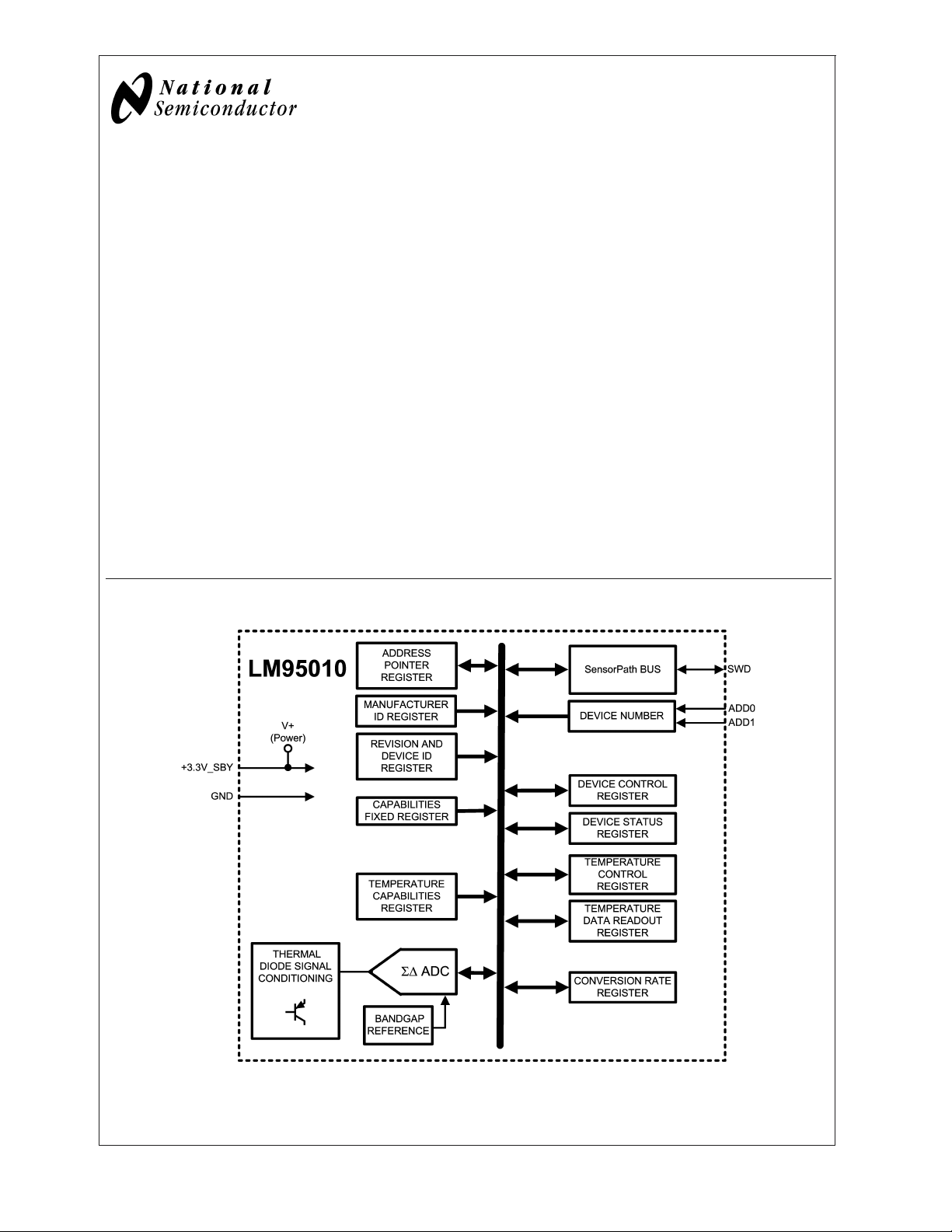
Block Diagram
n Temperature Sensing
— 0.25 ˚C resolution
— 127.75 ˚C maximum temperature reading
n 8-lead MSOP package
Key Specifications
n Temperature Sensor Accuracy
n Temperature Range −20 ˚C to +125 ˚C
n Power Supply Voltage +3.0V to +3.6V
n Power Supply Current 0.5 mA (typ)
n Conversion Time 14 ms to 1456 ms
Applications
n Microprocessor based equipment
— (Motherboards, Base-stations, Routers, ATMs, Point
of Sale, …)
n Power Supplies
™
Bus in
±
2 ˚C (max)
20082001
SensorPath™is a trademark of National Semiconductor Corporation.
© 2003 National Semiconductor Corporation DS200820 www.national.com
Page 2
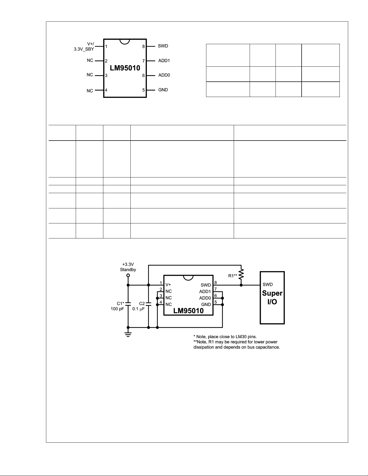
Connection Diagram
Ordering Information
LM95010
Order
Number
LM95010CIMM T19C MUA08A 1000 units in
LM95010CIMMX T19C MUA08A 3500 units in
20082002
Package
Marking
Pin Description
Pin
Number Pin Name Type Description Typical Connection
1 V+/3.3VSBPower Positive power supply pin +3.3V pin. Should be powered by +3.3V Standby power.
This pin should be bypassed with a 0.1 µF
capacitor. A bulk capacitance of approximately
10 µF needs to be in the near vicinity of the
LM95010.
2-4 NC Must be grounded.
5 GND Power Ground System ground
6 ADD0 Input Address select input that assigns the serial
bus device number
7 ADD1 Input Address select input that assigns the serial
bus device number
8 SWD Input/
Output
Single-wire Data, SensorPath serial
interface line; Open-drain output
10k resistor to V+ or GND; must never be left
floating
10k resistor to V+ or GND; must never be left
floating
Super I/O with 1.25k pull-up to 3.3V
NS
Package
Number
Transport
Media
tape and reel
tape and reel
Typical Application
FIGURE 1. LM95010 connection to SensorPath master such as a Super I/O.
20082003
www.national.com 2
Page 3

LM95010
Absolute Maximum Ratings
(Notes 1, 2)
Supply Voltage (V
Voltage on Pin 2 −0.3 V to (V+ + 0.3 V)
+
) −0.5 V to 6.0 V
Soldering Information, Lead Temperature
MSOP-8 Package (Note 6)
Vapor Phase (60 seconds) 215 ˚C
Infrared (15 seconds) 220 ˚C
Voltage on all other Pins −0.5 V to 6.0 V
Input Current per Pin(Note 3) 5 mA
Package Input Current (Note 3) 30 mA
Package Power Dissipation (Note 5)
Output Sink Current 10 mA
Storage Temperature −65 ˚C to +150 ˚C
ESD Susceptibility (Note 4)
Human Body Model 2000 V
Operating Ratings
(Notes 1, 2)
Temperature Range for
Electrical Characteristics T
LM95010CIMM −20 ˚C ≤ TA≤ +125 ˚C
Operating Temperature Range −20 ˚C ≤ T
Supply Voltage Range (V+) +3.0 V to +3.6 V
MIN
≤ TA≤ T
≤ +125 ˚C
A
Machine Model 200 V
DC Electrical Characteristics
The following specifications apply for V+ = 3.0 VDCto 3.6 VDC, unless otherwise specified in the conditions. Boldface limits
apply for T
A=TJ=TMIN
to T
POWER SUPPLY CHARACTERISTICS
Symbol Parameter Conditions
V+ Power Supply Voltage 3.3 3.0
I+
AVG
I+
Peak
Average Power Supply Current SensorPath Bus Inactive (Note
Peak Power Supply Current SensorPath Bus Inactive (Note
Power-On Reset Threshold Voltage 1.6 V (min)
TEMPERATURE-TO-DIGITAL CONVERTER CHARACTERISTICS
Parameter Conditions
Temperature Error T
Temperature Resolution 10 Bits
SWD and ADD DIGITAL INPUT CHARACTERISTICS
Symbol Parameter Conditions
SWD Logical High Input Voltage 2.1 V (min)
SWD Logical Low Input Voltage 0.8 V (max)
ADD Logical High Input Voltage 90%xV+ V (min)
ADD Logical Low Input Voltage 10%xV+ V (max)
SWD Input Hysteresis 300 mV
SWD and ADD Input Leakage
V
V
IH
V
IL
V
IH
V
IL
HYST
I
L
Current
SWD Input Leakage Current with V+
Open or Grounded
; all other limits TA= +25 ˚C.
MAX
= −20 ˚C and +125 ˚C (Note 10)
A
+25 ˚C ≤ T
T
A
GND ≤VIN≤ V+
GND ≤VIN≤ 3.6 V,
and V+ Open or
GND
Typical
(Note 7)
Limits
(Note 8)
Units
(Limit)
V (min)
3.6
V (max)
500 750 µA (max)
9)
1.6 mA
9)
2.8 V (max)
≤ +60 ˚C (Note 10)
A
Typical
(Note 7)
±
1
Limits
(Note 8)
±
3 ˚C (max)
±
2 ˚C (max)
Units
(Limits)
0.25 ˚C
Typical
(Note 7)
Limits
(Note 8)
Units
(Limit)
V+ + 0.5 V (max)
= 0 ˚C to +85 ˚C -0.5 V (min)
-0.3 V (min)
±
0.005
±
0.005 µA
±
10 µA (max)
MAX
www.national.com3
Page 4

SWD and ADD DIGITAL INPUT CHARACTERISTICS
Symbol Parameter Conditions
LM95010
C
IN
Digital Input Capacitance 10 pF
Typical
(Note 7)
Limits
(Note 8)
SWD DIGITAL OUTPUT CHARACTERISTICS
Symbol Parameter Conditions
V
OL
Open-drain Output Logic “Low”
Voltage
I
OH
C
OUT
Open-drain Output Off Current
Digital Output Capacitance 10 pF
IOL=4mA 0.4 V (max)
I
=50µA 0.2 V (max)
OL
Typical
(Note 7)
±
0.005
Limits
(Note 8)
±
10 µA (max)
AC Electrical Characteristics
The following specification apply for V+ = +3.0VDCto +3.6VDC, unless otherwise specified. Boldface limits apply for
T
A=TJ=TMIN
to T
cation. Please refer to that specification for further details.
HARDWARE MONITOR CHARACTERISTICS
Symbol Parameter Conditions
t
CONV
SensorPath Bus CHARACTERISTICS
Symbol Parameter Conditions
t
f
t
r
t
INACT
t
Mtr0
t
Mtr1
t
SFEdet
t
SLout1
t
MtrS
t
SLoutA
t
RST
t
RST_MAX
; all other limits TA=TJ= 25 ˚C. The SensorPath Characteristics conform to the SensorPath specifi-
MAX
Typical
(Note 7)
(Note 8)
Total Monitoring Cycle Time (Note 11) Default 182 163.8 ms (min)
Typical
SWD fall time (Note 12) R
SWD rise time (Note 13) R
= 1.25 kΩ
pull-up
±
30%, CL= 400 pF
=
pull-up
±
= 400 pF
L
30%,
1.25 kΩ
C
(Note 7)
(Note 8)
Minimum inactive time (bus at high level)
guaranteed by the LM95010 before an
Attention Request
Master drive for Data Bit 0 write and for
Data Bit 0-1read
Master drive for Data Bit 1 write 35.4 µs (min)
Time allowed for LM95010 activity
detection
LM95010 drive for Data Bit 1 read by
master
Master drive for Start Bit 80 µs (min)
LM95010 drive for Attention Request 165 µs (min)
Master or LM95010 drive for Reset 354 µs (min)
Maximum drive of SWD by an LM95010,
after the power supply is raised above 3V
Units
(Limit)
Units
(Limit)
Limits
Units
(Limits)
200.2 ms (max)
Limits
Units
(Limits)
300 ns (max)
1000 ns (max)
11 µs (min)
11.8 µs (min)
17.0 µs (max)
48.9 µs (max)
9.6 µs (max)
28.3 µs (min)
38.3 µs (max)
109 µs (max)
228 µs (max)
500 ms (max)
www.national.com 4
Page 5
LM95010
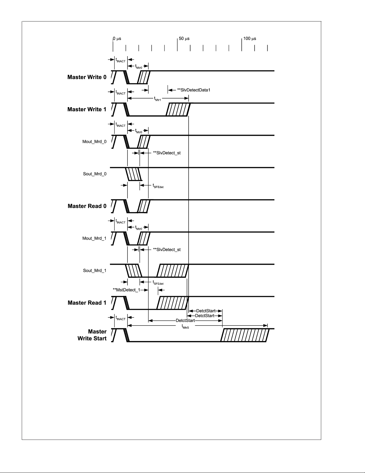
20082004
FIGURE 2. Timing for Data Bits 0, 1 and Start Bit. See Section 1.2 "Bit Signaling" for further details.
www.national.com5
Page 6
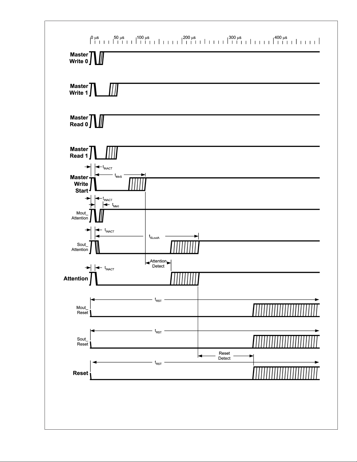
LM95010
FIGURE 3. Timing for Attention Request and Reset. See Section 1.2 "Bit Signaling" for further details.
www.national.com 6
20082005
Page 7

Note 1: Absolute Maximum Ratings indicate limits beyond which damage to the device may occur. Operating Ratings indicate conditions for which the device is
functional, but do not guarantee performance limits. For guaranteed specifications and test conditions, see the Electrical Characteristics. The guaranteed
specifications apply only for the test conditions listed. Some performance characteristics may degrade when the device is not operated under the listed test
conditions.
Note 2: All voltages are measured with respect to GND, unless otherwise noted.
Note 3: When the input voltage (V
components and/or ESD protection circuitry are shown below for the LM95010’s pins. The nominal breakdown voltage of D3 is 6.5 V. SNP stands for snap-back
device. Devices that are connected to a particular pin are marked with a"U" in the table below.
) at any pin exceeds the power supplies (V
IN
<
IN
GND or V
>
V+), the current at that pin should be limited to 5 mA. Parasitic
IN
LM95010
Pin Name PIN
#
D1 D2 D3 D4 D5 R1 SNP ESD CLAMP
V+/3.3V SB 1 UU
NC 2 UUUUUU U
NC 3
NC 4 UU UU U
ADD0 6 UU UU U
ADD1 7 UU U
SWD 8 UU UU U
20082006
FIGURE 4. ESD Protection Input Structure. Devices that are connected to a particular pin are marked with a"U"in
the table above.
Note 4: Human body model, 100 pF discharged through a 1.5 kΩ resistor. Machine model, 200 pF discharged directly into each pin. See Figure 4 above for the ESD
Protection Input Structure.
Note 5: Thermal resistance junction-to-ambient when attached to a printed circuit board with 2 oz. foil is 210 ˚C/W.
Note 6: See the URL “http://www.national.com/packaging/” for other recommendations and methods of soldering surface mount devices.
Note 7: “Typicals” are at T
Note 8: Limits are guaranteed to National’s AOQL (Average Outgoing Quality Level).
Note 9: The supply current will not increase substantially with SensorPath transactions.
Note 10: Temperature accuracy does not include the effects of self-heating. The rise in temperature due to self-heating is the product of the internal power
dissipation of the LM95010 and the thermal resistance. See (Note 5) for the thermal resistance to be used in the self-heating calculation.
Note 11: This specification is provided only to indicate how often temperature data is updated once enabled.
Note 12: The output fall time is measured from V
Note 13: The output rise time is measured from V
= 25 ˚C and represent most likely parametric norm. They are to be used as general reference values not for critical design calculations.
A
to V
IH min
IL max
. The output fall time is guaranteed by design.
IL max
to V
. The output rise time is guaranteed by design.
IH min
www.national.com7
Page 8

Typical Performance Characteristics
LM95010
Conversion Rate Effect on Power Supply Current
1.0 Functional Description
The LM95010 is based on a ∆Vbetemperature sensing
method. A differential voltage, representing temperature, is
digitized using a Sigma-Delta analog to digital converter. The
digital temperature data can be retrieved over a simple
single-wire interface called SensorPath. SensorPath has
been defined by National Semiconductor and is optimized
for hardware monitoring. National offers a royalty-free license in connection with its intellectual property rights in the
SensorPath bus.
The LM95010 has 2 address pins that allow up to 4
LM95010s to be connected to one SensorPath bus. The
physical interface of SensorPath’s SWD signal is identical to
the familiar industry standard SMBus SMBDAT signal. The
digital information is encoded in the pulse width of the signal
being transmitted. Every bit can be synchronized by the
master simplifying the implementation of the master when
implemented with a microcontroller. For microcontroller’s
with greater functionality an asynchronous attention signal
can be transmitted by the LM95010 to interrupt the microcontroller and notify it that temperature data has been updated in the readout register.
To optimize the LM95010’s power consumption to the system requirements, the LM95010 has a shutdown mode as
well as it supports multiple conversion rates.
1.1 SensorPath BUS SWD
SWD is the Single Wire Data line used for communication.
SensorPath uses 3.3V single-ended signaling, with a pull-up
resistor and open-drain low-side drive (see Figure 5). For
timing purposes SensorPath is designed for capacitive loads
) of up to 400pF. Note that in many cases a 3.3V standby
(C
L
rail of the PC will be used as a power supply for both the
sensor and the master. Logic high and low voltage levels for
SWD are TTL compatible. The master may provide an internal pull-up resistor. In this case the external resistor is not
needed. The minimum value of the pull-up resistor must take
into account the maximum allowable output load current of
4mA.
20082020
20082007
FIGURE 5. SensorPath SWD simplified schematic
1.2 SensorPath BIT SIGNALING
Signals are transmitted over SensorPath using pulse-width
encoding. There are five types of "bit signals":
Data Bit 0
•
Data Bit 1
•
Start Bit
•
Attention Request
•
Reset
•
All the "bit signals" involve driving the bus to a low level. The
duration of the low level differentiates between the different
"bit-signals". Each "bit signal" has a fixed pulse width. SensorPath supports a Bus Reset Operation and Clock Training
sequence that allows the slave device to synchronize its
internal clock rate to the master. Since the LM95010 meets
±
15% timing requirments of SensorPath, the LM95010
the
does not require the Clock Training sequence and does
support this feature. This section defines the "bit signal"
behavior in all the modes. Please refer to the timing diagrams in the Electrical Characteristics section (Figure 2 and
Figure 3) while going through this section. Note that the
timing diagrams for the different types of "bit signals" are
shown together to better highlight the timing relationships
between them. However, the different types of "bit signals"
appear on SWD at different points in time. These timing
diagrams show the signals as driven by the master and the
LM95010 slave as well as the signal as seen when probing
SWD. Signals labels that begin with the label Mout_ depict a
www.national.com 8
Page 9

1.0 Functional Description (Continued)
drive by the master. Signals labels that begin with the label
Slv_ depict the drive by the LM95010. All other signals show
what would be seen when probing SWD for a particular
function (e.g. "Master Wr 0" is the Master transmitting a Data
Bit with the value of 0).
1.2.1 Bus Inactive
The bus is inactive when the SWD signal is high for a period
of at least t
signal".
1.2.2 Data Bit 0 and 1
All Data Bit signal transfers are started by the master. A Data
Bit 0 is indicated by a "short" pulse; a Data Bit 1 is indicated
by a longer pulse. The direction of the bit is relative to the
master, as follows:
Data Write - a Data Bit transferred from the master to the
•
LM95010.
Data Read - a Data Bit transferred from the LM95010 to
•
the master.
A master must monitor the bus as inactive before starting a
Data Bit (read or Write).
A master initiates a data write by driving the bus active (low
level) for the period that matches the data value (t
for a write of "0" or "1", respectively). The LM95010 will
detect that the SWD becomes active within a period of
, and will start measuring the duration of that the SWD
t
SFEdet
is active in order to detect the data value.
A master initiates a data read by driving the bus for a period
. The LM95010 will detect that the SWD have become
of t
Mtr0
active within a period of t
LM95010 will not drive the SWD. For a data read of "1" the
LM95010 will start within t
period of t
the time at which the bus becomes inactive to identify a data
read of "0" or "1".
During each Data Bit, both the master and all the LM95010s
must monitor the bus (the master for Attention Request and
Reset; at the LM95010s for Start Bit, Attention Request and
Reset) by measuring the time SWD is active (low). If a Start
Bit, Attention Requests or Reset "bit signal" is detected, the
current "bit signal" is not treated as a Data Bit.
Note that the bit rate of the protocol varies depending on the
data transferred. Thus, the LM95010 has a value of "0" in
reserved or unused register bits for bus bandwidth efficiency.
1.2.3 Start Bit
A master must monitor the bus as inactive before beginning
a Start Bit.
The master uses a Start Bit to indicate the beginning of a
transfer. LM95010s will monitor for Start Bits all the time, to
allow synchronization of transactions with the master. If a
Start Bit occurs in the middle of a transaction, the LM95010
being addressed will abort the current transaction. In this
case the transaction is not "completed" by the LM95010 (see
Section 1.3 "SensorPath Bus Transactions").
During each Start Bit, both the master and all the LM95010s
must monitor the bus for Attention Request and Reset, by
. The bus is inactive between each "bit
INACT
. For a data read of "0", the
SFEdet
to drive the SWD low for a
. Both master and LM95010 must monitor
SLout1
SFEdet
Mtr0
or t
Mtr1
measuring the time SWD is active (low). If an Attention
Request or Reset condition is detected, the current "bit
signal" is not treated as a Start Bit. The master may attempt
to send the Start Bit at a later time.
1.2.4 Attention Request
The LM95010 may initiate an Attention Request when the
SensorPath bus is inactive.
Note that a Data Bit, or Start Bit, from the master may start
simultaneously with an Attention Request from the
LM95010. In addition, two LM95010s may start an Attention
Request simultaneously. Due to its length, the Attention Request has priority over any other "bit signal", except Reset.
Conflict with Data Bits and Start Bits are detected by all the
devices, to allow the bits to be ignored and re-issued by their
originator.
The LM95010 will either check to see that the bus is inactive
before starting an Attention Request, or start the Attention
Request with the t
active. The LM95010 will drive the signal low for t
time interval after SWD becomes
SFEdet
SLoutA
time.
After this, both the master and the LM95010 must monitor
the bus for a Reset Condition. If a Reset condition is detected, the current "bit signal" is not treated as an Attention
Request.
After Reset, an Attention Request can not be sent before the
master has sent 14 Data Bits on the bus. See Section 1.3.5
for further details on Attention Request generation.
1.2.5 Bus Reset
The LM95010 issues a Reset at power up. The master must
also generate a Bus Reset at power-up for at least the
minimum reset time, it must not rely on the LM95010. SensorPath puts no limitation on the maximum reset time of the
master. Following a Bus Reset, the LM95010 may generate
an Attention Request only after the master has sent 14 Data
Bits on the bus. See section 1.3.5 for further details on
Attention Request generation.
1.3 SensorPath BUS TRANSACTIONS
SensorPath is designed to work with a single master and up
to seven slave devices. Each slave has a unique address.
The LM95010’s supports up to 4 device addresses that are
selected by the state of the address pins ADD0 and ADD1.
The Register Set of the LM95010 is defined in Section 2.0.
1.3.1 Bus Reset Operation
A Bus Reset Operation is global on the bus and affects only
the communication interface of all the devices connected to
it. The Bus Reset operation does not affect either the contents of the device registers, or device operation, to the
extent defined in LM95010 Register Set, see Section 2.0.
The Bus Reset operation is performed by generating a Reset
signal on the bus. The master must apply Reset after powerup, and before it starts operation. The Reset signal end will
be monitored by all the LM95010s on the bus.
After the Reset Signal the SensorPath specification requires
that the master send a sequence of 8 Data Bits with a value
of "0", without a preceding Start Bit. This is required to
enable slaves that "train" their clocks to the bit timing. The
LM95010 does not require nor does it support clock training.
LM95010
www.national.com9
Page 10

1.0 Functional Description (Continued)
LM95010
20082008
FIGURE 6. Bus Reset Transaction
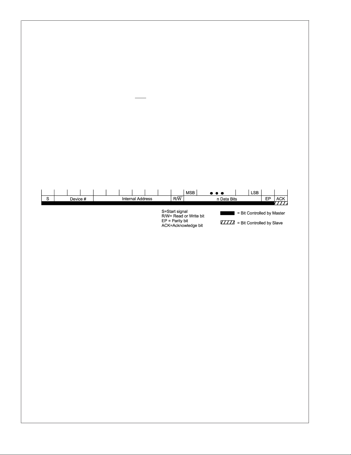
1.3.2 Read Transaction
During a read transaction, the master reads data from a
register at a specified address within a slave. A read transaction begins with a Start Bit and ends with an ACK bit, as
shown in Figure 7.
Device Number This is the address of the LM95010
•
device accessed. Address "000" is a broadcast address
and can be responded to by all the slave devices. The
LM95010 ignores the broadcast address during a read
transaction.
Internal Address The address of a register within the
•
LM95010 that is read.
Read/Write (R/W) A "1" indicates a read transaction.
•
Data Bits During a read transaction the data bits are
•
driven by the LM95010. Data is transferred serially with
the most significant bit first. This allows throughput optimization based on the information that needs to be read.
The LM95010 supports 8-bit or 16-bit data fields, as
described in Section 2.0 "Register Set".
Even Parity (EP) This bit is based on all preceding bits
•
(device number, internal address, read/write and data
bits) and the parity bit itself. The parity -number of 1’s - of
all the preceding bits and the parity bit must be even - i.e.,
the result must be 0. During a read transaction, the EP bit
is sent by the LM95010 to the master to allow the master
to check the received data before using it.
Acknowledge (ACK) During a read transaction the ACK
•
bit is sent by the master indicating that the EP bit was
received and was found to be correct, when compared to
the data preceding it, and that no conflict was detected
on the bus (excluding Attention Request - see Section
1.3.5 "Attention Request Transaction"). A read transfer is
considered "complete" only when the ACK bit is received.
A transaction that was not positively acknowledged is not
considered "complete" by the LM95010 and following are
performed:
— The BER bit in the LM95010 Device Status register is
set
— The LM95010 generates an Attention Request before,
or together with the Start Bit of the next transaction
A transaction that was not positively acknowledged is
also not considered "complete" by the master (i.e. internal operations related to the transaction are not performed). The transaction may be repeated by the master,
after detecting the source of the Attention Request (the
LM95010 that has a set BER bit in the Device Status
register). Note that the SensorPath protocol neither
forces, nor automates re-execution of the transaction by
the master.
The values of the ACK bit are:
— 1: Data was received correctly
— 0: An error was detected (no-acknowledge).
FIGURE 7. Read Transaction, master reads data from LM95010
1.3.3 Write Transaction
In a write transaction, the master writes data to a register at
a specified address in the LM95010. A write transaction
begins with a Start Bit and ends with an ACK Data Bit, as
show in Figure 8.
Device Number This is the address of the slave device
•
accessed. Address "000" is a broadcast address and is
responded to by all the slave devices. The LM95010
responds to broadcast messages to the Device Control
Register.
www.national.com 10
20082009
Internal Address This is the register address in the
•
LM95010 that will be written.
Read/Write (R/W) A "0" data bit directs a write transac-
•
tion.
Page 11
1.0 Functional Description (Continued)
Data Bits This is the data written to the LM95010 regis-
•
ter, are driven by the master. Data is transferred serially
with the most significant bit first. The number of data bits
may vary from one address to another, based on the size
of the register in the LM95010. This allows throughput
optimization based on the information that needs to be
written.
The LM95010 supports 8-bit or 16-bit data fields, as
described in Section 2.0 "Register Set".
Even Parity (EP) This data bit is based on all preceding
•
bits (Device Number, Internal Address, Read/Write and
Data bits) and the Even Parity bit itself. The parity (number of 1’s) of all the preceding bits and the parity bit must
be even - i.e. the result must be 0. During a write transaction, the EP bit is sent by the master to the LM95010 to
allow the LM95010 to check the received data before
using it.
Acknowledge (ACK) During the write transaction the
•
ACK bit is sent by the LM95010 indicating to the master
that the EP was received and was found correct, and that
no conflict was detected on the bus (excluding Attention
Request - see Section 1.3.5 "Attention Request Transac-
LM95010
tion"). A write transfer is considered "completed" only
when the ACK bit is generated. A transaction that was not
positively acknowledged is not considered complete by
the LM95010 (i.e. internal operation related to the transaction are not performed) and the following are performed:
— The BER bit in the LM95010 Device Status register is
set;
— The LM95010 generates an Attention Request before,
or together with the Start Bit of the next transaction
A transaction that was not positively acknowledged is
also not considered "complete" by the master (i.e. internal operations related to the transaction are not performed). The transaction may be repeated by the master,
after detecting the source of the Attention Request (the
LM95010 that has a set BER bit in the Device Status
register). Note that the SensorPath protocol neither
forces, nor automates re-execution of the transaction by
the master.
The values of the ACK bit are:
— 1: Data was received correctly;
— 0: An error was detected (no-acknowledge).
FIGURE 8. Write Transaction, master write data to LM95010
1.3.4 Read and Write Transaction Exceptions
This section describes master and LM95010 handling of
special bus conditions, encountered during either Read or
Write transactions.
If an LM95010 receives a Start Bit in the middle of a transaction, it aborts the current transaction (the LM95010 does
not "complete" the current transaction) and begins a new
transaction. Although not recommend for SensorPath normal
operation, this situation is legitimate, therefore it is not
flagged as an error by the LM95010 and Attention Request is
not generated in response to it. The master generating the
Start Bit, is responsible for handling the not "complete" transaction at a "higher level".
If LM95010 receives more than the expected number of data
bits (defined by the size of the accessed register), it ignores
the unnecessary bits. In this case, if both master and
LM95010 identify correct EP and ACK bits they "complete"
the transaction. However, in most cases, the additional data
bits differ from the correct EP and ACK bits. In this case, both
the master and the LM95010 do not "complete" the transaction. In addition, the LM95010 performs the following:
the BER bit in the LM95010 Device Status register is set
•
the LM95010 generates an Attention Request
•
If the LM95010 receives less than the expected number of
data bits (defined by the size of the accessed register), it
waits indefinitely for the missing bits to be sent by the
20082010
master. If then the master sends the missing bits, together
with the correct EP/ACK bits, both master and LM95010
"complete" the transaction. However, if the master starts a
new transaction generating a Start Bit, the LM95010 aborts
the current transaction (the LM95010 does not "complete"
the current transaction) and begins the new transaction. The
master is not notified by the LM95010 of the incomplete
transaction.
1.3.5 Attention Request Transaction
Attention Request is generated by the LM95010 when it
needs the attention of the master. The master and all
LM95010s must monitor the Attention Request to allow bit
re-sending in case of simultaneous start with a Data Bit or
Start Bit transfer. Refer to the "Attention Request" section,
Section 1.2.4 in the "Bit Signaling" portion of the data sheet.
The LM95010 will generate an Attention Request using the
following rules:
1. A Function event that sets the Status Flag has occurred
and Attention Request is enabled and
2. The "physical" condition for an Attention Request is met
(i.e., the bus is inactive), and
3. At the first time 2 is met after 1 occurred, there has not
been an Attention request on the bus since a read of the
Device Status register, or since a Bus Reset.
OR
www.national.com11
Page 12

1.0 Functional Description (Continued)
1. A bus error event occurred, and
LM95010
2. the "physical" condition for an Attention Request is met
(i.e., the bus is inactive), and
3. At the first time 2. is met after 1 occurred, there has not
been a Bus Reset.
All devices (master or slave) must monitor the bus for an
Attention Request signal. The following notes clarify the
intended system operation that uses the Attention Request
Indication.
Masters are expected to use the attention request as a
•
trigger to read results from the LM95010. This is done in
a sequence that covers all LM95010s. This sequence is
referred to as "master sensor read sequence".
After an Attention Request is sent by an LM95010 until
•
after the next read from the Device Status register the
LM95010 does not send Attention Requests for a function
event since it is guaranteed that the master will read the
Status register as part of the master sensor read sequence. Note that the LM95010 will send an attention for
BER, regardless of the Status register read, to help the
master with any error recovery operations and prevent
deadlocks.
2.0 Register Set
2.1 REGISTER SET SUMMARY
A master must record the Attention Request event. It
•
must then scan all slave devices in the system by reading
their Device Status register and must handle any pending
event in them before it may assume that there are no
more events to handle.
Note: there is no indication of which slave has sent the
request. The requirement that multiple requests are not sent
allows the master to know within one scan of register reads
that there are no more pending events.
1.3.6 Fixed Number Setting
The LM95010 device number is defined by strapping of the
ADD0 and ADD1 pins. The LM95010 will wake (after Device
Reset) with the Device Number field of the Device Number
register set to the address as designated in Section 1.1.1
Device Number. It is the responsibility of the system designer to avoid having two devices with the same Device
Number on the bus.
Devices should be detected by the master by a read operation of the Device Number register. The read returns "000" if
there is no device at that address on the bus (the EP bit must
be ignored).
P
Reg
Register
Add
000 000
000 001 ManufacturerIDR 100Bh 0001000000001011
000 010 Device ID R 21h RevID Device ID
000 011 Capabilities
000 100 Device
000 101 Device
001 000 Temperature
001 001 Temperature
001 010 Temperature
001 011
-011 111
100 000 Conversion
100 001
- 111 111
Name
Device
Number
Fixed
Status
Control
Capabilities
Data
Readout
Control
Reserved R Undefined
Rate
Undefined
Registers
R/
W
R * Not Available
R 1h Reserved Function 1
R 0h Not Available BER 0 0 ERF1 0 0 0 SF1
R/W0h Reserved EnF1 Res Low
R 014Ah Reserved Int
R MSb
R/W0h Reserved EN0 ATE
R/W2h Not Available 000000Conversion
R Undefined
Bit
O
R
Val
Bit14Bit13Bit12Bit11Bit10Bit9Bit8Bit7Bit6Bit5Bit4Bit3Bit2Bit
15
MSb
Reserved
00000
0000000000100001
0000000000000001
00000000000 0
Rout
Sign 10Bits 0.25˚C
Sens
Size
0000000101001010
64˚C 32˚C 16˚C 8˚C 4˚C 2˚C 1˚C 0.5˚CLSb
Sign
00000000000000
0.25
000000
˚C
Pwr
Reserved
See Table 1
Resolution
1
Shut
down
Bit
0
LSb
Reset
Rate
www.national.com 12
Page 13

2.0 Register Set (Continued)
* Depends on state of ADD pins see Table 1.
2.2 Device Reset Operation
A Device Reset operation is performed in the following conditions:
At device power-up.
•
When the Reset bit in the Device Control register is set to 1 (see Section 2.8 "Device Control").
•
The Device Reset operation performs the following:
Aborts any device operation in progress and restarts device operation.
•
Sets all device registers to their "Reset" (default) value.
•
2.3 DEVICE NUMBER (Addr 00o)
This register is used to specify a unique address for each device on the bus.
P
Reg Add Register Name
000 000 Device Number R 4h-1h
The value of AS2:AS0 is determined by the setting of the ADD0 and ADD1 input pins:
TABLE 1. Device Number Assignment
[ADD1:ADD0] [AS2:AS0]
00 001
01 010
R/
W
O
R
Val
Bit 7 Bit 6 Bit 5 Bit 4 Bit 3 Bit 2 Bit 1
Reserved
00000
[ADD1:ADD0] [AS2:AS0]
10 011
11 100
LM95010
Bit 0
LSb
AS2 AS1 AS0
The value of AS2:AS0 will directly change and follow the value determined by ADD1:ADD0. Since this is a read only register the
value of the address cannot be changed by software.
2.4 MANUFACTURER ID (Addr 01o)
P
Reg
Add
000 001
The manufacturer ID matches that assigned to National Semiconductor by the PCI SIG. This register may be used to identify the
manufacturer of the device in order to perform manufacturer specific operations.
2.5 DEVICE ID (Addr 02o)
Reg
Add
000 010 Device ID R 21h
The device ID is defined by the manufacturer of the device and is unique for each device produced by a manufacturer. Bits 15-11
identify the revision number of die and will be incremented upon revision of the device.
Register
Name
Manufacturer
ID
Register
Name
Bit Type Description
10-0 RO DeviceID (Device ID Value) A fixed value that identifies the device.
15-11 RO RevID (Revision ID Value) A fixed value that identifies the device revision.
R/
W
R 100Bh 0001000000001011
R/
W
Bit
O
R
Val
P
O
R
Val
Bit14Bit13Bit12Bit11Bit10Bit9Bit8Bit7Bit6Bit5Bit4Bit3Bit2Bit
15
MSb
Bit
Bit14Bit13Bit12Bit11Bit10Bit9Bit8Bit7Bit6Bit5Bit4Bit3Bit2Bit
15
MSb
RevID DeviceID
0000000000100001
1
1
Bit
0
LSb
Bit
0
LSb
www.national.com13
Page 14

2.0 Register Set (Continued)
2.6 CAPABILITIES FIXED (Addr 03o)
LM95010
P
Reg
Register
Add
000 011
The value of this register defines the capabilities of the LM95010. The LM95010 supports only one function, that of Temperature
Measurement type. Please refer to the SensorPath specification for further details on other FuncDescriptor values.
2.7 DEVICE STATUS (Addr 04o)
This register is set to the reset value by a Device Reset.
Reg Add Register Name
Name
Capabilities
Fixed
000 100 Device Status R 0h BER 0 0 ERF1 0 0 0 SF1
Bit Type Description
0ROSF1 (Status Function 1). This bit is set by a Function Event within Function 1. Event details are function
3-1 RO Not supported. Will always read "0".
4ROERF1 (Error Function 1) This bit is set in response to an error indication within Function 1. ERF1 is cleared
6-5 RO Not supported. Will always read "0".
7ROBER (Bus Error). This bit is set when the device either generates, or receives an error indication in the ACK
R/
W
R1h
dependent and are described within the function. SF1 is cleared by Device Reset or by handling the event
within the function (see Section 2.9 for further details).
0: Status flag for Function 1 is inactive (no event).
1: Status flag for Function 1 is active indicating that a Function Event has occurred.
by Device Reset or by handling the error condition within the function (see Section 2.9 for further details).
0: No error occurred in Function 1.
1: Error occurred in Function 1.
bit of the transaction (i.e., no-acknowledge). BER is cleared by Device Reset or by reading the Device Status
register.
0: No transaction error occurred.
1: An ACK bit error (no-acknowledge) occurred during the last transaction.
Bit
O
R
Val
Bit14Bit13Bit12Bit11Bit10Bit9Bit8Bit7Bit6Bit5Bit4Bit3Bit2Bit
15
MSb
Reserved FuncDescriptor1
0000000000000001
P
R/
W
O
R
Val
Bit 7 Bit 6 Bit 5 Bit 4 Bit 3 Bit 2 Bit 1
1
Bit
0
LSb
Bit 0
LSb
2.8 DEVICE CONTROL (Addr 05o)
This register responds to a broadcast write command (DeviceNumber 000). Write using broadcast address is ignored by bits
15-2. This register is set to the reset value by a Device Reset.
P
Reg
Register
Add
000 101
www.national.com 14
Name
Device
Control
Bit Type Description
0 R/W Reset (Device Reset). When set to "1" this bit initiates a Device Reset operation ( See Section 2.2). This bit
R/
W
R/
W
self-clears after the Device Reset operation is completed.
0: Normal device operation. (default)
1: Device Reset
The LM95010 does not require a Device Reset command after power.
Bit
O
R
Val
0h
Bit14Bit13Bit12Bit11Bit
15
MSb
00000000000
10
Reserved
Bit8Bit7Bit6Bit5Bit4Bit3Bit2Bit
Bit9
EnF1 Res
Low
Pwr
Bit
1
LSb
Shut
downReset
0
Page 15

2.0 Register Set (Continued)
Bit Type Description
1 R/W Shutdown (Shutdown Mode). When set to "1" this bit stops the operation of all functions and places the
device in the lowest power consumption mode.
0: Device in Active Mode. (default)
1: Device in Shutdown Mode.
2 R/W LowPwr (Low-Power Mode). When set to "1" this bit slows the operation of all functions and places the
device in a low power consumption mode. In Low-Power Mode, the conversion rate of the LM95010 is
effected see Section 2.10 for further details.
0: Device in Active Mode. (default)
1: Device in Low-Power Mode.
3RONot supported. Will always read "0".
4 R/W EnF1 (Enable Function 1). When bit is set to "1" this bit Function 1 is enabled for operation. A function may
require setup before this bit is set. The function registers can be accessed even when the function is
disabled.
0: Function 1 is disabled. (default)
1: Function is enabled.
15-5 RO Not supported. Will always read "0".
2.9 TEMPERATURE MEASUREMENT FUNCTION (TYPE - 0001)
This section defines the register structure and operation of a Temperature Measurement function as it applies to the LM95010.
The FuncDescriptor value of this function is ‘0001’.
LM95010
2.9.1 Operation
The Temperature Measurement function as implemented in the LM95010 supports one temperature zone, the LM95010’s internal
temperature (LM95010’s junction temperature). Since the LM95010 only supports one temperature measurement the Sensor
Scan function as defined in the SensorPath specification only applies to one temperature sensor. A temperature scan is enabled
by the SensorEnable bit (EN0). The minimum scan rate is recommended to be 4Hz (i.e. the measurement data is updated at least
once in 250 ms), see Section 2.10 for further details. In Low-Power Mode, the scan rate is four time lower than the scan rate in
Active Mode. The scan rate effects the bus bandwidth required to read the results. The sampling rate of the temperature
measurements can also be controlled via the Conversion Rate register, see Section 2.10 for further details.
Data Readout When a new result is stored in the Readout register a Function Event is generated. Reading the Readout
register clears the Status Function 1 flag (SF1). The result is available in the Readout register waiting for the master to read it
during the master sensor read sequence. If a new result is ready before the previous result has been read, the new result
overwrites the previous result and the Error Function 1 flag (ERF1) is set (indicating an overrun event). Reading the Readout
register clears also the Error Function 1 flag (ERF1). The Readout register contains the temperature data, and the sensor number.
Since the LM95010 only supports one temperature zone the sensor number field will always report zero. Other fields in the
Readout register as defined by the SensorPath specification are not supported.
Readout Resolution The resolution of the readout is defined in the Temperature Capabilities register. The resolution of the
LM95010 is fixed and cannot be modified by software.
Function Event The Temperature Measurement function generates a Function Event whenever a temperature conversion
cycle is completed and new data is stored in the Readout Register. When the new data is stored into the Readout register the SF1
bit in the device Status register is set to "1" and remains set, until it is cleared by reading the Readout register. An Attention
Request is generated on the bus, only if it is enabled by the Attention Enable bit (ATE) in the Temperature Control register.
Setup Before Enabling No setup is required for the Temperature Measurement function before the function is enabled.
2.9.2 Temperature Capabilities (Addr 10o)
P
Reg
Add
001 000
Register
Name
Temperature
Capabilities
R/
W
R 014Ah
Bit
O
R
Val
Bit14Bit13Bit12Bit11Bit10Bit9Bit8Bit7Bit6Bit5Bit4Bit3Bit2Bit
15
MSb
Int
Reserved
0000000101001010
Sens
Rout
Sign 10Bits
Size
1
0.25˚C
Resolution
Bit
0
LSb
This register defines the format of the temperature data in the readout register. The LM95010 only supports one format as defined
by the values of this register.
www.national.com15
Page 16

2.0 Register Set (Continued)
LM95010
Bit Type Description
2-0 R Resolution. This field defines the value of 1 LSb of the Temperature Readout field in the Readout Register.
The SensorPath specification defines many different weights for the temperature LSb. The LM95010
supports a resolution of 0.25 ˚C and thus a value of 010 for this field. For a full definition of this field please
refer to the SensorPath specification.
5-3 R Number of Bits. This field defines the total number of significant bits of the Temperature Readout field in the
Readout register. The total number of osignificant bits includes the number of bits representing the interger
part of the temperature data and the fractional part of it, as defined by the Resolution field. The LM95010
supports 10 bits and thus a value of 001 for this field. For a full definition of this field please refer to the
SensorPath specification.
6RSign (Signed Data). Defines the type of data in the Temperature Readout field of the Readout register.
0: Unsigned, positive fixed point value.
1: Signed, 2’s complement fixed point value. (value for the LM95010)
7RRoutSize (Readout Register size). Defines the total size of the Readout register.
0: 16 bits. (LM95010 default)
1: 24 bits.
8 R/W IntSens (Internal Sensor Support). Indicates if the device supports internal temperature measurements, as
the LM95010 does.
0: No internal temperature measurement
1: Internal temperature sensor implemented. (value for the LM95010)
15-9 RO Reserved. Will always read "0".
2.9.3 Temperature Data Readout (Addr 11o)
P
Reg
Register
Add
001 001
The LM95010’s temperature data format is two’s complement and has 10-bits of resolution with the LSb having a weight of
0.25 ˚C. The LM95010 can resolve temperature between +127.75 ˚C and -128 ˚C, inclusive. It can measure temperatures
between +127.75 ˚C and −20 ˚C with an accuracy of
Name
Temperature
Data
Readout
R/
W
R
Decimal Binary Hex
+127.75 ˚C 01 1111 1111 1FFh
+100.00 ˚C 01 1001 0000 190h
+1.00 ˚C 00 0000 0100 004h
+0.25 ˚C 00 0000 0001 001h
0 ˚C 00 0000 0000 000h
-0.25 ˚C 11 1111 1111 3FFh
-1.00 ˚C 11 1111 1100 3FCh
-20.00 ˚C 11 1011 0000 3 B0h
-39.75 ˚C 11 0110 0001 361h
-40.00 ˚C 11 0110 0000 360h
-128.00 ˚C 10 0000 0000 200h
O
R
Val
Bit
Bit14Bit13Bit12Bit11Bit10Bit9Bit8Bit7Bit6Bit5Bit4Bit3Bit2Bit
15
MSb
MSb
64˚C 32˚C 16˚C 8˚C 4˚C 2˚C 1˚C
Sign
±
3.0 ˚C.
Temperature Data Format
0.5
˚C
LSb
0.25
000000
˚C
1
Reserved
Bit
0
LSb
www.national.com 16
Page 17

2.0 Register Set (Continued)
2.9.4 Temperature Control (Addr 12o)
This register is set to the reset value by a Device Reset.
P
Reg
Add
001 010
Bit Type Description
15-2 R Reserved. Will allways read "0".
Register
Name
Temperature
ControlR/W
0RATE (Attention Enable). When set, this bit enables an Attention Request signal to generated by the
1REN0 (Enable Sensor). When this bit is set, the Temperature Sensor is enabled for temperature
R/
W
LM95010, if the EN0 bit is set.
0: Attention Request disabled (from enabled Temperature Sensor- default)
1: Attention Request enabled
measurements.
0: Temperature Sensor disabled (default)
1: Temperature Sensor enabled
Bit
O
R
Val
0h00000000000000
Bit14Bit13Bit12Bit11Bit10Bit9Bit8Bit7Bit6Bit5Bit4Bit3Bit2Bit
15
MSb
Reserved
Bit
0
1
LSb
EN0 ATE
LM95010
2.10 CONVERSION RATE (Addr 40o)
P
Reg Add Register Name
100 000 Conversion Rate
LowPwr Conversion Rate[1:0] Typical Conversion Rate (ms)
000 14
100 91
001 91
1 01 364
0 10 182 (default)
1 10 728
0 11 364
1 11 1456
The temperature conversion rate is controlled by this register as well as the Low Power Bit of Device Control Register. This
register is not defined by the SensorPath specification. Therefore, it must be accessed during BIOS run time. The conversion rate
is dependent on system physical requirements and limitations. The thermal response time of the MSOP package is one such
requirement.
R/
W
R/
W
O
R
Val
2h000000Conversion Rate
Bit 7 Bit 6 Bit 5 Bit 4 Bit 3 Bit 2 Bit 1
Bit 0
LSb
www.national.com17
Page 18

3.0 Applications Information
3.1 MOUNTING CONSIDERATIONS
LM95010
The LM95010 can be applied easily in the same way as
other integrated-circuit temperature sensors. It can be glued
or cemented to a surface. The temperature that the
LM95010 is reading will typically be within +0.2 ˚C of the
surface temperature to which the LM95010’s leads are attached to.
This presumes that the ambient air temperature is almost the
same as the surface temperature; if the air temperature were
much higher or lower than the surface temperature, the
actual temperature measured would be at an intermediate
temperature between the surface temperature and the air
temperature.
Alternatively, the LM95010 can be mounted inside a sealedend metal tube, and can then be dipped into a bath or
screwed into a threaded hole in a tank. As with any IC, the
LM95010 and accompanying wiring and circuits must be
kept insulated and dry, to avoid leakage and corrosion. This
is especially true if the circuit may operate at cold temperatures where condensation can occur. Printed-circuit coatings
and varnishes such as Humiseal and epoxy paints or dips
are often used to ensure that moisture cannot corrode the
LM95010 or its connections.
The thermal resistance junction to ambient (θ
) is the pa-
JA
rameter used to calculate the rise of a device junction temperature due to its power dissipation. For the LM95010 the
equation used to calculate the rise in the die temperature is
as follows: T
where I
is the quiescent current (500 µA typ.), VOLis the
Q
logic "Low" output level of SWD, and I
+ θJAx [(V+xIQ)+(VOLxIOL)]
J=TA
is the load current
OL
on SWD. Since the LM95010’s junction temperature is the
actual temperature being measured care should be taken to
minimize the load current that the LM95010 is require to
drive. When mounted to a PCB, with 2 oz. copper foil, the
LM95010’s thermal resistance is typically 210 ˚C/W.
www.national.com 18
Page 19

Physical Dimensions inches (millimeters)
unless otherwise noted
LM95010 Digital Temperature Sensor with SensorPath Bus in MSOP8 Package
8-Lead Molded Mini Small Outline Package (MSOP),
JEDEC Registration Number MO-187,
Order Number LM95010CIMM, or LM95010CIMMX,
NS Package Number MUA08A
LIFE SUPPORT POLICY
NATIONAL’S PRODUCTS ARE NOT AUTHORIZED FOR USE AS CRITICAL COMPONENTS IN LIFE SUPPORT
DEVICES OR SYSTEMS WITHOUT THE EXPRESS WRITTEN APPROVAL OF THE PRESIDENT AND GENERAL
COUNSEL OF NATIONAL SEMICONDUCTOR CORPORATION. As used herein:
1. Life support devices or systems are devices or
systems which, (a) are intended for surgical implant
into the body, or (b) support or sustain life, and
whose failure to perform when properly used in
accordance with instructions for use provided in the
2. A critical component is any component of a life
support device or system whose failure to perform
can be reasonably expected to cause the failure of
the life support device or system, or to affect its
safety or effectiveness.
labeling, can be reasonably expected to result in a
significant injury to the user.
BANNED SUBSTANCE COMPLIANCE
National Semiconductor certifies that the products and packing materials meet the provisions of the Customer Products
Stewardship Specification (CSP-9-111C2) and the Banned Substances and Materials of Interest Specification
(CSP-9-111S2) and contain no ‘‘Banned Substances’’ as defined in CSP-9-111S2.
National Semiconductor
Americas Customer
Support Center
Email: new.feedback@nsc.com
Tel: 1-800-272-9959
www.national.com
National does not assume any responsibility for use of any circuitry described, no circuit patent licenses are implied and National reserves the right at any time without notice to change said circuitry and specifications.
National Semiconductor
Europe Customer Support Center
Fax: +49 (0) 180-530 85 86
Email: europe.support@nsc.com
Deutsch Tel: +49 (0) 69 9508 6208
English Tel: +44 (0) 870 24 0 2171
Français Tel: +33 (0) 1 41 91 8790
National Semiconductor
Asia Pacific Customer
Support Center
Email: ap.support@nsc.com
National Semiconductor
Japan Customer Support Center
Fax: 81-3-5639-7507
Email: jpn.feedback@nsc.com
Tel: 81-3-5639-7560
 Loading...