

Page 1
April 2004
LM93
Hardware Monitor with Integrated Fan Control for Server
Management
1.0 General Description
The LM93, hardware monitor, has a two wire digital interface
compatible with SMBus 2.0. Using an 8-bit Σ∆ ADC, the
LM93 measures the temperature of two remote diode connected transistors as well as its own die and 16 power supply
voltages.
To set fan speed, the LM93 has two PWM outputs that are
each controlled by up to four temperature zones. The fancontrol algorithm is lookup table based. The LM93 includes a
digital filter that can be invoked to smooth temperature readings for better control of fan speed. The LM93 has four
tachometer inputs to measure fan speed. Limit and status
registers for all measured values are included.
The LM93 builds upon the functionality of previous motherboard management ASICs and uses some of the LM85’s
features (i.e. smart tachometer mode). It also adds measurement and control support for dynamic Vccp monitoring and
PROCHOT. It is designed to monitor a dual processor Xeon
class motherboard with a minimum of external components.
2.0 Features
n 8-bit Σ∆ ADC
n Monitors 16 power supplies
n Monitors 2 remote thermal diodes
n Internal ambient temperature sensing
n Programmable autonomous fan control based on
temperature readings with fan boost support
n Fan control based on 13-step lookup table
n Temperature reading digital filter
n 1.0˚C digital temperature sensor resolution
n 0.5˚C temperature resolution for fan control
n 2 PWM fan speed control outputs
n 4 fan tachometer inputs
n Dual processor thermal throttling (PROCHOT)
monitoring
n Dual dynamic VID monitoring (6 VIDs per processor)
n 8 general purpose I/Os:
— 4 can be configured as fan tachometer inputs
— 2 can be configured to connect to THERMTRIP from
a processor
— 2 are standard GPIOs that could be used to monitor
IERR signal
n 2 general purpose inputs that can be used to monitor
SCSI termination signals
n Limit register comparisons of all monitored values
n 2-wire, SMBus 2.0 compliant, serial digital interface
— Supports byte/block read and write
— Configurable slave address (tri-level pin selects 1 of
3 possible addresses)
n 2.5V reference voltage output
n 56-pin TSSOP package
n XOR-tree test mode
3.0 Key Specifications
n Voltage Measurement Accuracy
n Resolution 8-bits, 1˚C
n Temperature Sensor Accuracy
n Temperature Range:
— LM93 Operational 0˚C to +85˚C
— Remote Temp Accuracy 0˚C to +125˚C
n Power Supply Voltage +3.0V to +3.6V
n Power Supply Current 0.9 mA
±
2% FS (max)
±
3˚C (max)
4.0 Applications
n Servers
n Workstations
n Multi-Microprocessor based equipment
LM93 Hardware Monitor with Integrated Fan Control for Server Management
5.0 Ordering Information
Order Number NS Package Number Transport media
LM93CIMT MTD56 34 units in rail
LM93CIMTX MTD56 1000 units in tape-and-reel
I2C is a registered trademark of the Philips Corporation.
© 2004 National Semiconductor Corporation DS200682 www.national.com
Page 2
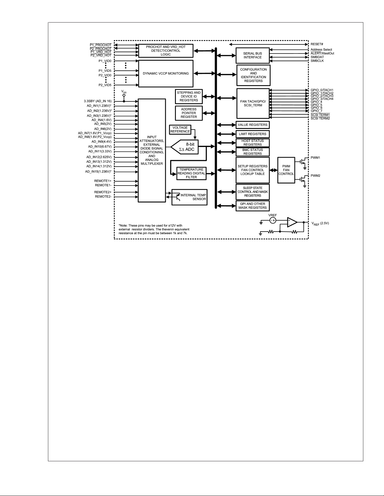
6.0 Block Diagram
LM93
20068201
www.national.com 2
Page 3

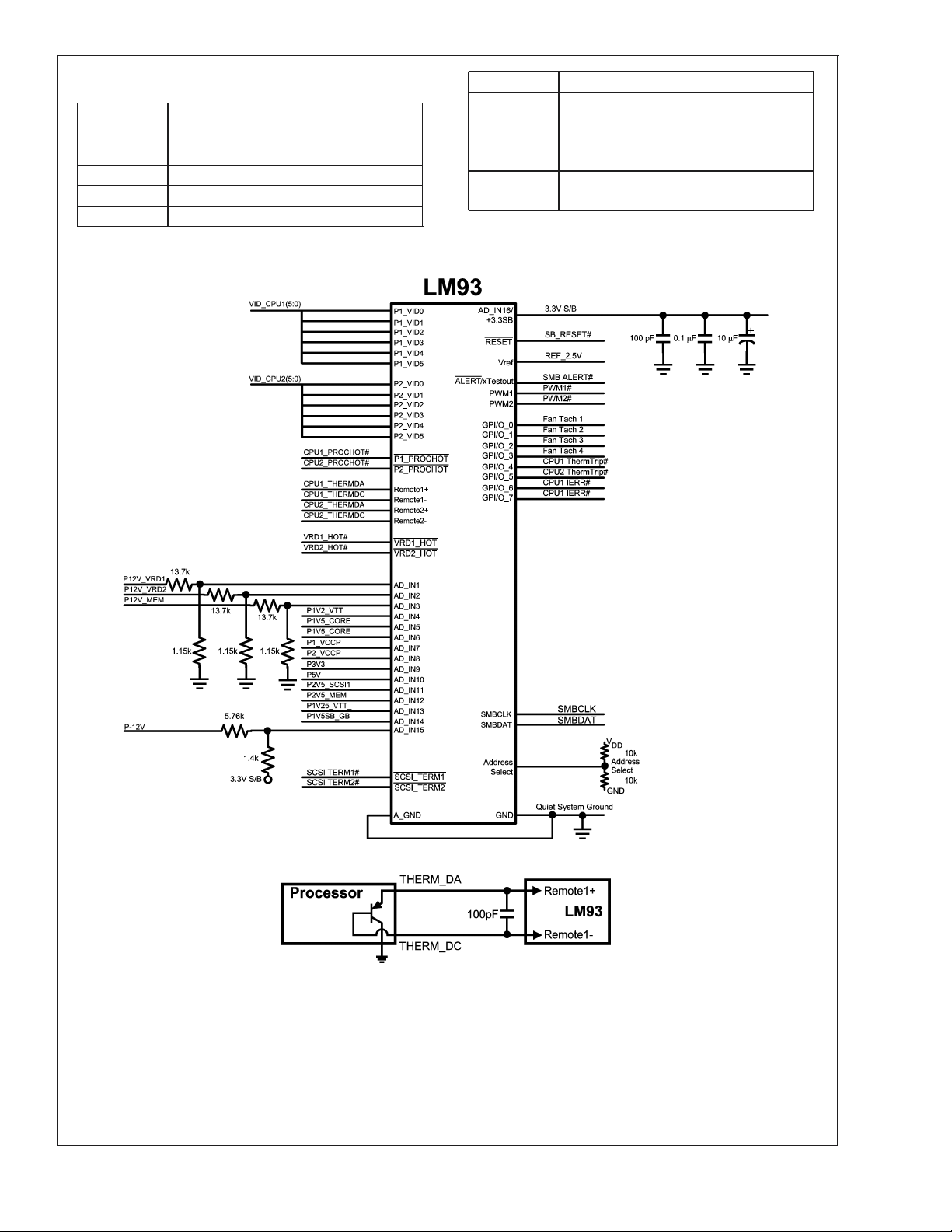
7.0 Application
Baseboard management of a Dual processor server. Two
LM93s may be required to manage a quad processor base-
2 Way Xeon Server Management
LM93
board. The block diagram of LM93 hardware is illustrated
below. The hardware implementation is a single chip ASIC
solution.
20068205
www.national.com3
Page 4

LM93
1.0 General Description ..................................................................................................................................... 1
Table of Contents
2.0 Features ....................................................................................................................................................... 1
3.0 Key Specifications ........................................................................................................................................ 1
4.0 Applications .................................................................................................................................................. 1
5.0 Ordering Information .................................................................................................................................... 1
6.0 Block Diagram .............................................................................................................................................. 2
7.0 Application .................................................................................................................................................... 3
8.0 Connection Diagram .................................................................................................................................... 7
9.0 Pin Descriptions ........................................................................................................................................... 8
10.0 Server Terminology .................................................................................................................................. 10
11.0 Recommended Implementation ................................................................................................................ 11
12.0 Functional Description .............................................................................................................................. 12
12.1 MONITORING CYCLE TIME ................................................................................................................ 12
12.2 Σ∆ A/D INHERENT AVERAGING .......................................................................................................... 12
12.3 TEMPERATURE MONITORING ........................................................................................................... 12
12.3.1 Temperature Data Format ............................................................................................................... 12
12.3.2 Thermal Diode Fault Status ............................................................................................................. 12
12.4 VOLTAGE MONITORING ...................................................................................................................... 12
12.5 RECOMMENDED EXTERNAL SCALING RESISTORS FOR +12V POWER RAILS .......................... 13
12.6 RECOMMENDED EXTERNAL SCALING CIRCUIT FOR −12V POWER INPUT ................................ 13
12.7 DYNAMIC Vccp MONITORING USING VID ......................................................................................... 15
12.8 V
OUTPUT ....................................................................................................................................... 15
REF
12.9 PROCHOT BACKGROUND INFORMATION ........................................................................................ 15
12.10 PROCHOT MONITORING .................................................................................................................. 16
12.11 PROCHOT OUTPUT CONTROL ........................................................................................................ 16
12.12 FAN SPEED MEASUREMENT ........................................................................................................... 17
12.13 SMART FAN SPEED MEASUREMENT ............................................................................................. 17
13.0 Inputs/Outputs .......................................................................................................................................... 17
13.1 ALERT OUTPUT ................................................................................................................................... 17
13.2 RESET INPUT/OUTPUT ....................................................................................................................... 17
13.3 PWM1 AND PWM2 OUTPUTS ............................................................................................................. 17
13.4 SCSI_TERMx INPUTS .......................................................................................................................... 17
13.5 VRD1_HOT AND VRD2_HOT INPUTS ................................................................................................ 18
13.6 GPIO PINS ............................................................................................................................................ 18
13.7 FAN TACH INPUTS ............................................................................................................................... 18
14.0 SMBus Interface ....................................................................................................................................... 18
14.1 SMBUS ADDRESSING ......................................................................................................................... 18
14.2 DIGITAL NOISE EFFECT ON SMBUS COMMUNICATION ................................................................. 18
14.3 GENERAL SMBUS TIMING .................................................................................................................. 18
14.4 SMBUS ERROR SAFETY FEATURES ................................................................................................ 19
14.5 SERIAL INTERFACE PROTOCOLS ..................................................................................................... 19
14.5.1 Address Incrementing ...................................................................................................................... 19
14.5.2 Block Command Code Summary .................................................................................................... 20
14.5.3 Write Operations ............................................................................................................................. 20
14.5.3.1 Write Byte ................................................................................................................................... 20
14.5.3.2 Write Word ................................................................................................................................. 20
14.5.3.3 SMBus Write Block to Any Address ........................................................................................... 21
14.5.3.4 I
2
C™Block Write ....................................................................................................................... 21
14.5.4 Read Operations .............................................................................................................................. 22
14.5.4.1 Read Byte .................................................................................................................................. 22
14.5.4.2 Read Word ................................................................................................................................. 22
14.5.4.3 SMBus Block-Write Block-Read Process Call ........................................................................... 22
14.5.4.4 Simulated SMBus Block-Write Block-Read Process Call .......................................................... 24
14.5.4.5 SMBus Fixed Address Block Reads .......................................................................................... 24
14.5.4.6 I
2
C Block Reads ......................................................................................................................... 25
14.6 READING AND WRITING 16-BIT REGISTERS ................................................................................... 25
15.0 Using The LM93 ....................................................................................................................................... 26
15.1 POWER ON .......................................................................................................................................... 26
15.2 RESETS ................................................................................................................................................ 26
15.3 ADDRESS SELECTION ........................................................................................................................ 26
15.4 DEVICE SETUP .................................................................................................................................... 26
15.5 ROUND ROBIN VOLTAGE/TEMPERATURE CONVERSION CYCLE ................................................. 26
www.national.com 4
Page 5

Table of Contents (Continued)
15.6 ERROR STATUS REGISTERS ............................................................................................................. 27
15.6.1 ASF Mode ........................................................................................................................................ 27
15.7 MASKING, ERROR STATUS AND ALERT ........................................................................................... 27
15.8 LAYOUT AND GROUNDING ................................................................................................................ 27
15.9 THERMAL DIODE APPLICATION ......................................................................................................... 27
15.9.1 Accuracy Effects of Diode Non-Ideality Factor ................................................................................ 28
15.9.2 PCB Layout for Minimizing Noise .................................................................................................... 28
15.10 FAN CONTROL ................................................................................................................................... 28
15.10.1 Automatic Fan Control Algorithm ................................................................................................... 28
15.10.2 Fan Control Temperature Resolution ............................................................................................ 30
15.10.3 Zone 1-4 to PWM1-2 Binding ........................................................................................................ 31
15.10.4 Fan Control Duty Cycles ............................................................................................................... 31
15.10.5 Alternate PWM Frequencies .......................................................................................................... 31
15.10.6 Fan Control Priorities ..................................................................................................................... 31
15.10.7 PWM to 100% Conditions ............................................................................................................. 31
15.10.8 VRDx_HOT Ramp-Up/Ramp-Down .............................................................................................. 32
15.10.9 PROCHOT Ramp-Up/Ramp-Down ............................................................................................... 32
15.10.10 Manual PWM Override ................................................................................................................ 32
15.10.11 Fan Spin-Up Control .................................................................................................................... 32
15.11 XOR TREE TEST ................................................................................................................................ 33
16.0 Registers .................................................................................................................................................. 34
16.1 REGISTER WARNINGS ....................................................................................................................... 34
16.2 REGISTER SUMMARY TABLE ............................................................................................................. 34
16.3 FACTORY REGISTERS 00h–3Fh ........................................................................................................ 40
16.3.1 Register 00h XOR Test ................................................................................................................. 40
16.3.2 Register 01h SMBus Test ............................................................................................................. 40
16.3.3 Register 3Eh Manufacturer ID ...................................................................................................... 40
16.3.4 Register 3Fh Version/Stepping ..................................................................................................... 40
16.4 BMC ERROR STATUS REGISTERS 40h–47h .................................................................................... 41
16.4.1 Register 40h B_Error Status 1 ...................................................................................................... 41
16.4.2 Register 41h B_Error Status 2 ...................................................................................................... 42
16.4.3 Register 42h B_Error Status 3 ...................................................................................................... 42
16.4.4 Register 43h B_Error Status 4 ...................................................................................................... 43
16.4.5 Register 44h B_P1_PROCHOT Error Status ............................................................................... 43
16.4.6 Register 45h B_P2_PROCHOT Error Status ............................................................................... 44
16.4.7 Register 46h B_GPI Error Status .................................................................................................. 44
16.4.8 Register 47h B_Fan Error Status .................................................................................................. 45
16.5 HOST ERROR STATUS REGISTERS .................................................................................................. 45
16.5.1 Register 48h H_Error Status 1 ...................................................................................................... 45
16.5.2 Register 49h H_Error Status 2 ...................................................................................................... 46
16.5.3 Register 4Ah H_Error Status 3 ..................................................................................................... 47
16.5.4 Register 4Bh H_Error Status 4 ..................................................................................................... 48
16.5.5 Register 4Ch H_P1_PROCHOT Error Status ............................................................................... 49
16.5.6 Register 4Dh B_P2_PROCHOT Error Status ............................................................................... 50
16.5.7 Register 4Eh H_GPI Error Status ................................................................................................. 51
16.5.8 Register 4Fh H_Fan Error Status ................................................................................................. 52
16.6 VALUE REGISTERS ............................................................................................................................. 52
16.6.1 Registers 50–53h Unfiltered Temperature Value Registers ......................................................... 52
16.6.2 Registers 54–55h Filtered Temperature Value Registers ............................................................. 52
16.6.3 Register 56–65h A/D Channel Voltage Registers ........................................................................ 53
16.6.4 Register 67h Current P1_PROCHOT ........................................................................................... 53
16.6.5 Register 68h Average P1_PROCHOT .......................................................................................... 54
16.6.6 Register 69h Current P2_PROCHOT ........................................................................................... 54
16.6.7 Register 6Ah Average P2_PROCHOT ......................................................................................... 54
16.6.8 Register 6Bh GPI State ................................................................................................................. 55
16.6.9 Register 6Ch P1_VID .................................................................................................................... 55
16.6.10 Register 6Dh P2_VID .................................................................................................................. 55
16.6.11 Register 6E–75h Fan Tachometer Readings .............................................................................. 56
16.7 LIMIT REGISTERS ................................................................................................................................ 57
16.7.1 Registers 78–7Fh Temperature Limit Registers ........................................................................... 57
16.7.2 Registers 80–83h Fan Boost Temperature Registers .................................................................. 57
LM93
www.national.com5
Page 6

LM93
16.7.3 Registers 90–AFh Voltage Limit Registers ................................................................................... 58
16.7.4 Register B0–B1h PROCHOT User Limit Registers ...................................................................... 59
16.7.5 Register B2–B3h Dynamic Vccp Limit Offset Registers ............................................................... 60
16.7.6 Register B4–BBh Fan Tach Limit Registers ................................................................................. 61
16.8 SETUP REGISTERS ............................................................................................................................. 62
16.8.1 Register BCh Special Function Control 1 (Voltage Hysteresis and Fan Control Filter Enable) ... 62
16.8.2 Register BDh Special Function Control 2 (Smart Tach Mode Enable and Fan Control Temperature
Resolution Control) ..................................................................................................................................... 63
16.8.3 Register BEh GPI/VID Level Control ............................................................................................63
16.8.4 Register BFh PWM Ramp Control ................................................................................................ 64
16.8.5 Register C0h Fan Boost Hysteresis (Zones 1/2) .......................................................................... 64
16.8.6 Register C1h Fan Boost Hysteresis (Zones 3/4) .......................................................................... 65
16.8.7 Register C2h Zones 1/2 Spike Smoothing Control ....................................................................... 65
16.8.8 Register C3h Zones 1/2 MinPWM and Hysteresis ....................................................................... 66
16.8.9 Register C4h Zones 3/4 MinPWM and Hysteresis ....................................................................... 66
16.8.10 Register C5h GPO ...................................................................................................................... 67
16.8.11 Register C6h PROCHOT Override .............................................................................................. 68
16.8.12 Register C7h PROCHOT Time Interval ...................................................................................... 69
16.8.13 Register C8h PWM1 Control 1 ................................................................................................... 70
16.8.14 Register C9h PWM1 Control 2 ................................................................................................... 71
16.8.15 Register CAh PWM1 Control 3 ................................................................................................... 72
16.8.16 Register CBh Special Function PWM1 Control 4 ....................................................................... 72
16.8.17 Register CCh PWM2 Control 1 ................................................................................................... 73
16.8.18 Register CDh PWM2 Control 2 ................................................................................................... 74
16.8.19 Register CEh PWM2 Control 3 ................................................................................................... 75
16.8.20 Register CFh Special Function PWM2 Control 4 ....................................................................... 75
16.8.21 Register D0h–D3h Zone 1 to 4 Base Temperatures .................................................................. 76
16.8.22 Register D4h–DFh Lookup Table Steps— Zone 1/2 and Zone 3/4 Offset Temperature ........... 76
16.8.23 Register E0h Special Function TACH to PWM Binding .............................................................. 77
16.8.24 Register E2h LM93 Status Control .............................................................................................78
16.8.25 Register E3h LM93 Configuration ............................................................................................... 79
16.9 SLEEP STATE CONTROL AND MASK REGISTERS .......................................................................... 80
16.9.1 Register E4h Sleep State Control ................................................................................................ 80
16.9.2 Register E5h S1 GPI Mask ........................................................................................................... 81
16.9.3 Register E6h S1 Tach Mask ......................................................................................................... 81
16.9.4 Register E7h S3 GPI Mask ........................................................................................................... 82
16.9.5 Register E8h S3 Tach Mask ......................................................................................................... 82
16.9.6 Register E9h S3 Temperature/Voltage Mask ................................................................................ 82
16.9.7 Register EAh S4/5 GPI Mask ....................................................................................................... 83
16.9.8 Register EBh S4/5 Temperature/Voltage Mask ............................................................................ 83
16.10 OTHER MASK REGISTERS ............................................................................................................... 84
16.10.1 Register ECh GPI Error Mask ..................................................................................................... 84
16.10.2 Register EDh Miscellaneous Error Mask .................................................................................... 84
16.10.3 Register EEh Special Function Zone 1 Adjustment Offset ......................................................... 85
16.10.4 Register EFh Special Function Zone 2 Adjustment Offset ......................................................... 85
17.0 Absolute Maximum Ratings ..................................................................................................................... 86
18.0 Operating Ratings ................................................................................................................................... 86
19.0 Data Sheet Version History ...................................................................................................................... 91
20.0 Physical Dimensions ................................................................................................................................ 92
Table of Contents (Continued)
www.national.com 6
Page 7

8.0 Connection Diagram
LM93
56 Pin TSSOP
NS Package MTD56
Top View
NS Order Numbers:
LM93CIMT (34 units per rail), or
LM93CIMTX (1000 units per tape-and-reel)
20068202
www.national.com7
Page 8
9.0 Pin Descriptions
LM93
Symbol Pin # Type Function
GPIO_0/TACH1 1 Digital I/O
(Open-Drain)
GPIO_1/TACH2 2 Digital I/O
(Open-Drain)
GPIO_2/TACH3 3 Digital I/O
(Open-Drain)
GPIO_3/TACH4 4 Digital I/O
(Open-Drain)
GPIO_4 /
P1_THERMTRIP
GPIO_5 /
P2_THERMTRIP
5 Digital I/O
(Open-Drain)
6 Digital I/O
(Open-Drain)
GPIO_6 7 Digital I/O
(Open-Drain)
GPIO_7 8 Digital I/O
(Open-Drain)
VRD1_HOT
9 Digital Input CPU1 voltage regulator HOT
Can be configured as fan tach input or a general purpose
open-drain digital I/O.
Can be configured as fan tach input or a general purpose
open-drain digital I/O.
Can be configured as fan tach input or a general purpose
open-drain digital I/O.
Can be configured as fan tach input or a general purpose
open-drain digital I/O..
A general purpose open-drain digital I/O. Can be configured to
monitor a CPU’s THERMTRIP signal to mask other errors.
A general purpose open-drain digital I/O. Can be configured to
monitor a CPU’s THERMTRIP signal to mask other errors.
Can be used to detect the state of CPU1 IERR or a general purpose
open-drain digital I/O
Can be used to detect the state of CPU2 IERR or a general purpose
open-drain digital I/O
VRD2_HOT 10 Digital Input CPU2 voltage regulator HOT
SCSI_TERM1 11 Digital Input SCSI Channel 1 termination fuse. Could also be used as a general
purpose input to trigger an error event.
SCSI_TERM2
12 Digital Input SCSI Channel 2 termination fuse. Could also be used as a general
purpose input to trigger an error event.
SMBDAT 13 Digital I/O
(Open-Drain)
Bidirectional System Management Bus Data. Output configured as
5V tolerant open-drain. SMBus 2.0 compliant.
SMBCLK 14 Digital Input System Management Bus Clock. Driven by an open-drain output,
and is 5V tolerant. SMBus 2.0 Compliant.
ALERT/XtestOut
15 Digital Output
(Open-Drain)
Open-drain ALERT output used in an interrupt driven system to
signal that an error event has occurred. Masked error events do not
activate the ALERT output. When in XOR tree test mode, functions
as XOR Tree output.
RESET
16 Digital I/O
(Open-Drain)
Open-drain reset output when power is first applied to the LM93.
Used as a reset for devices powered by 3.3V stand-by. After reset,
this pin becomes a reset input. See section 6.2 for more information.
AGND 17 GROUND Input Analog Ground
V
REF
18 Analog Output 2.5V used for external ADC reference, or as a V
REF
reference
voltage
REMOTE1− 19 Remote Thermal
Diode_1- Input (CPU
1 THERMDC)
This is the negative input (current sink) from the CPU1 thermal
diode. Connected to THERMDC pin of Pentium processor or the
emitter of a diode connected MMBT3904 NPN transistor. Serves as
the negative input into the A/D for thermal diode voltage
measurements. A 100 pF capacitor is optional and can be
connected between REMOTE1− and REMOTE1+.
REMOTE1+ 20 Remote Thermal
Diode_1+ I/O (CPU1
THERMDA)
This is a positive connection to the CPU1 thermal diode. Serves as
the positive input into the A/D for thermal diode voltage
measurements. It also serves as a current source output that
forward biases the thermal diode. Connected to THERMDA pin of
Pentium processor or the base of a diode connected MMBT3904
NPN transistor. A 100 pF capacitor is optional and can be
connected between REMOTE1− and REMOTE1+.
www.national.com 8
Page 9

9.0 Pin Descriptions (Continued)
Symbol Pin # Type Function
REMOTE2− 21 Remote Thermal
Diode_2 - Input
(CPU2 THERMDC)
REMOTE2+ 22 Remote Thermal
Diode_2 + I/O (CPU2
THERMDA)
AD_IN1 23 Analog Input (+12V1) Analog Input for +12V Rail 1 monitoring, for CPU1 voltage regulator.
AD_IN2 24 Analog Input (+12V2) Analog Input for +12V Rail 2 monitoring, for CPU2 voltage regulator.
AD_IN3 25 Analog Input (+12V3) Analog Input for +12V Rail 3, for Memory/3GIO slots. External
AD_IN4 26 Analog Input
(FSB_Vtt)
AD_IN5 27 Analog Input (3GIO /
PXH / MCH_Core)
AD_IN6 28 Analog Input
(ICH_Core)
AD_IN7 (P1_Vccp) 29 Analog Input
(CPU1_Vccp)
AD_IN8 (P2_Vccp) 30 Analog Input
(CPU2_Vccp)
AD_IN9 31 Analog Input (+3.3V) Analog input for +3.3V monitoring.
AD_IN10 32 Analog Input (+5V) Analog input for +5V monitoring silver box supply monitoring.
AD_IN11 33 Analog Input
(SCSI_Core)
AD_IN12 34 Analog Input
(Mem_Core)
AD_IN13 35 Analog Input
(Mem_Vtt)
AD_IN14 36 Analog Input
(Gbit_Core)
AD_IN15 37 Analog Input (-12V) Analog input for -12V monitoring. External resistors required to scale
Address Select 38 3 level analog input This input selects the lower two bits of the LM93 SMBus slave
This is the negative input (current sink) from the CPU2 thermal
diode. Connected to THERMDC pin of Pentium processor or the
emitter of a diode connected MMBT3904 NPN transistor. Serves as
the negative input into the A/D for thermal diode voltage
measurements. A 100 pF capacitor is optional and can be
connected between REMOTE2− and REMOTE2+.
This is a positive connection to the CPU2 thermal diode. Serves as
the positive input into the A/D for thermal diode voltage
measurements. It also serves as a current source output that
forward biases the thermal diode. Connected to THERMDA pin of
Pentium processor or the base of a diode connected MMBT3904
NPN transistor. A 100 pF capacitor is optional and can be
connected between REMOTE2− and REMOTE2+.
External attenuation resistors required such that 12V is attenuated
to 0.927V.
External attenuation resistors required such that 12V is attenuated
to 0.927V.
attenuation resistors required such that 12V is attenuated to 0.927V.
Analog input for 1.2V monitoring
Analog input for 1.5V monitoring.
Analog input for 1.5V monitoring.
Analog input for +Vccp (processor voltage) monitoring.
Analog input for +Vccp (processor voltage) monitoring.
Analog input for +2.5V monitoring.
Analog input for +1.969V monitoring.
Analog input for +0.984V monitoring.
Analog input for +0.984V S/B monitoring.
to positive level. Full scale reading at 1.236V.
address.
LM93
www.national.com9
Page 10

9.0 Pin Descriptions (Continued)
LM93
Symbol Pin # Type Function
AD_IN16 39 POWER (V
standby power
GND 40 GROUND Digital Ground. Digital ground and analog ground need to be tied
PWM1 41 Digital Output
(Open-Drain)
PWM2 42 Digital Output
(Open-Drain)
P1_VID0 43 Digital Input Voltage Identification signal from the processor.
P1_VID1 44 Digital Input Voltage Identification signal from the processor.
P1_VID2 45 Digital Input Voltage Identification signal from the processor.
P1_VID3 46 Digital Input Voltage Identification signal from the processor.
P1_VID4 47 Digital Input Voltage Identification signal from the processor.
P1_VID5 48 Digital Input Voltage Identification signal from the processor.
P1_PROCHOT
P2_PROCHOT
P2_VID0 51 Digital Input Voltage Identification signal from the processor.
P2_VID1 52 Digital Input Voltage Identification signal from the processor.
P2_VID2 53 Digital Input Voltage Identification signal from the processor.
P2_VID3 54 Digital Input Voltage Identification signal from the processor.
P2_VID4 55 Digital Input Voltage Identification signal from the processor.
P2_VID5 56 Digital Input Voltage Identification signal from the processor.
49 Digital I/O
(Open-Drain)
50 Digital I/O
(Open-Drain)
) +3.3V
DD
VDDpower input for LM93. Generally this is connected to +3.3V
standby power.
The LM93 can be powered by +3.3V if monitoring in low power
states is not required, but power should be applied to this input
before any other pins.
This pin also serves as the analog input to monitor the 3.3V
stand-by (SB) voltage. It is necessary to bypass this pin with a 0.1
µF in parallel with 100 pF. A bulk capacitance of 10 µF should be in
the near vicinity. The 100 pF should be closest to the power pin.
together at the chip then both taken to a low noise system ground.
A voltage difference between analog and digital ground may cause
erroneous results.
Fan control output 1.
Fan control output 2
Connected to CPU1 PROCHOT (processor hot) signal through a
bidirectional level shifter.
Connected to CPU2 PROCHOT (processor hot) signal through a
bi-directional level shifter.
The overscore indicates the signal is active low (“Not”).
10.0 Server Terminology
A/D Analog to Digital Converter
ACPI Advanced Configuration and Power
Interface
ALERT
ASF Alert Standard Format
BMC Baseboard Micro-Controller
BW Bandwidth
DIMM Dual inline memory module
DP Dual-processor
ECC Error checking and correcting
FRU Field replaceable unit
FSB Front side bus
www.national.com 10
SMBus signal to bus master that an event
occurred that has been flagged for
attention.
FW Firmware
Gb Gigabit
GB Gigabyte
Gbe Gigabit Ethernet
GPIO General purpose I/O
HW Hardware
2
I
C Inter integrated circuit (bus)
LAN Local area network
LVDS Low-Voltage Differential Signaling
Mb Megabit
MB Megabyte
MP Multi-processor
MTBF Mean time between failures
Page 11
LM93
10.0 Server Terminology (Continued)
MTTR Mean time to repair
NIC Network Interface Card (Ethernet Card)
OS Operating system
P/S Power Supply
PCI PCI Local Bus
PDB Power Distribution Board
11.0 Recommended Implementation
POR Power On Reset
PS Power Supply
SMBCLK and
SMBDAT
VRD Voltage Regulator Down - regulates Vccp
These signals comprise the SMBus
interface (data and clock) See the SMBus
Interface section for more information.
voltage for a CPU
Note: 100 pF cap is optional and should be placed close to the LM93, if used. The maximum capacitance between these pins is 300 pF.
20068207
20068206
www.national.com11
Page 12
12.0 Functional Description
LM93
The LM93 provides 16 channels of voltage monitoring, two
remote thermal diode monitors, an onboard ambient temperature sensor, 2 PROCHOT monitors, 4 fan tachometers,
8 GPIOs, THERMTRIP monitor for masking error events, 2
SCSI_TERM inputs, and all the associated limit registers on
a single chip, which communicates to the rest of the baseboard over the System Management Bus (SMBus).
Readings from both the external thermal diodes and the
internal temperature sensor are made available as an 8-bit
two’s-complement digital byte with the LSB representing
1˚C.
All but 4 of the analog inputs include internal scaling resistors. External scaling resistors are required for measuring
±
12V. The inputs are converted to 8-bit digital values such
that a nominal voltage appears at
ages and
1
⁄4scale for negative voltages. The analog inputs
3
⁄4scale for positive volt-
are intended to be connected to both baseboard resident
VRDs and to standard voltage rails supplied by a SSI compliant power supply.
The LM93 provides a number of internal registers, which are
detailed in the register section of this document.
12.1 MONITORING CYCLE TIME
When the LM93 is powered up, it cycles through each temperature measurement followed by the analog voltages in
sequence, and it continuously loops through the sequence.
The total monitoring cycle time is not more than 100 ms, as
this is the time period that most external micro-controllers
require to read the register values.
Each measured value is compared to values stored in the
limit registers. When the measured value violates the programmed limit, a corresponding status bit in the B_ and
H_Error Status Registers is set.
The PROCHOT and dynamic VID/Vccp monitoring is performed independently of the analog and temperature monitoring cycle.
12.2 Σ∆ A/D INHERENT AVERAGING
The Σ∆ A/D architecture filters the input signal. During one
conversion many samples are taken of the input voltage and
these samples are effectively averaged to give the final
result. The output of the Σ∆ A/D is the average value of the
signal during the sampling interval. For a voltage measurement, the samples are accumulated for 1.5 ms. For a temperature measurement, the samples are accumulated for
8.4 ms.
12.3 TEMPERATURE MONITORING
The LM93 remote diode target is the embedded thermal
diode found in a Xeon class processor. In some cases
instead of using the embedded thermal diode, found on the
Xeon processor, a diode connected 2N3904 transistor type
can also be used. An example of this would be a MMBT3904
with its collector and base tied to the thermal diode REMOTE+ pin and the emitter tied to the thermal diode
REMOTE− pin. Since the MMBT3904 is a surface mount
device and has very small thermal mass, it measures the
board temperature where it is mounted. The non-ideality and
series resistance varies for different diodes. Since the LM93
is optimized for the Xeon processor, when measuring a
2N3904 transistor an offset in the error band of approximately −4˚C may be observed. This can be corrected for by
programming the appropriate Zone Adjustment Offset register.
The LM93 acquires temperature data from three different
sources:
2 external diodes (embedded in a processor or discrete)
1 internal diode (internal to the LM93)
In addition to these three temperatures, a fourth temperature
can be externally written into the LM93 from the SMBus. This
value can be used to control fans, or compared against
limits, etc. The temperature value registers are located at
addresses 50h–53h. The temperature sources are referred
to as “zones” for convenience:
Zone Description
Zone 1 Processor 1 remote diode
(REMOTE1+, REMOTE1−)
Zone 2 Processor 2 remote diode
(REMOTE2+, REMOTE2−)
Zone 3 Internal LM93 on-chip sensor
Zone 4 External Digital Sensor written in from SMBus
12.3.1 Temperature Data Format
Most of the temperature data for the LM93 is represented in
a common format. The format is an 8-bit, twos complement
byte with the LSB equal to 1.0 ˚C. This applies to temperature measurements as well as any temperature limit registers and some configuration registers. Some fan control
configuration registers use four bits and have a binary format, please see the fan control configuration register descriptions for further details on this 4-bit format.
Temperature Binary Hex
+125˚C 0111 1101 7Dh
+25˚C 0001 1001 19h
+1.0˚C 0000 0001 01h
0˚C 0000 0000 00h
−1.0˚C 1111 1111 FFh
−25˚C 1110 0111 E7h
−55˚C 1100 1001 C9h
−127˚C 1000 0001 81h
Note: A value of 80h has a special meaning in the limit registers. It means
that the temperature channel is masked. In addition, temperature readings of
80h indicate thermal diode faults.
12.3.2 Thermal Diode Fault Status
The LM93 provides for indications of a fault (open or short
circuit) with the remote thermal diodes. Before a remote
diode conversion is updated, the status of the remote diode
is checked for an open or short circuit condition. If such a
fault condition occurs, a status bit is set in the status register.
A short circuit is defined as the input pins being connected to
each other. When an open or short circuit is detected, the
corresponding temperature register is set to 80h.
12.4 VOLTAGE MONITORING
The LM93 contains inputs for monitoring voltages. Scaling is
such that the correct value refers to approximately 3/4 scale
±
or 192 decimal on all inputs except the
12V. Input voltages
are converted by an 8-bit Delta-Sigma (∆Σ) A/D. The DeltaSigma A/D architecture provides inherent filtering and spike
smoothing of the analog input signal.
±
12V inputs must be scaled externally. A full scale
The
reading is achieved when 1.236V is applied to these inputs.
For optimum performance the +12V should be scaled to
www.national.com 12
Page 13
12.0 Functional Description
(Continued)
provide a nominal
should be scaled to provide a nominal
thevenin resistance at the pin should be kept between 1 kΩ
and7kΩ.
The −12V monitoring is particularly challenging. It is required
3
⁄4full scale reading, while the −12V
1
⁄4scale reading. The
to bring the −12V rail into the positive input voltage region of
the A/D input. It is suggested that the supply rail for the LM93
device be used as the offset voltage. This voltage is usually
derived from the P/S 5V stand-by voltage rail via a
accurate linear regulator. In this fashion we can always
assume that the offset voltage is present when the −12V rail
is present as the system cannot be turned on without the
3.3V stand-by voltage being present.
that an external offset voltage and external resistors be used
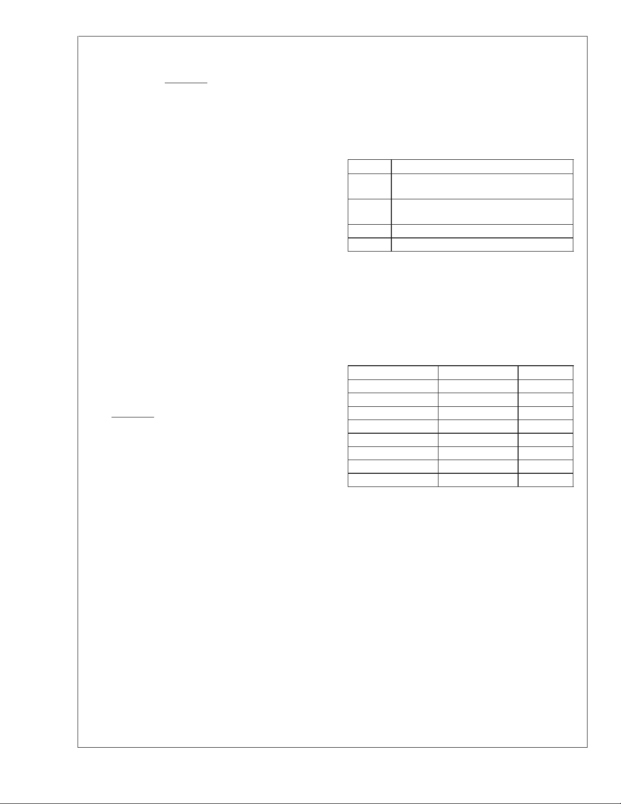
Voltage vs Register Reading
Register
Reading
at
Nominal
Maximum
Voltage
Pin
Normal
Use
Nominal
Voltage
Voltage
AD_IN1 +12V1 0.927V C0h 1.236V FFh 0V 00h −0.3V to (V
AD_IN2 +12V2 0.927V C0h 1.236V FFh 0V 00h −0.3V to (V
AD_IN3 +12V3 0.927V C0h 1.236V FFh 0V 00h −0.3V to (V
Register
Reading at
Maximum
Voltage
Minimum
Voltage
Register
Reading at
Minimum
Voltage
Absolute
Maxmum Range
+ 0.05V)
DD
+ 0.05V)
DD
+ 0.05V)
DD
AD_IN4 FSB_Vtt 1.20V C0h 1.60V FFh 0V 00h −0.3V to +6.0V
AD_IN5 3GIO 1.5V C0h 2V FFh 0V 00h −0.3V to +6.0V
AD_IN6 ICH_Core 1.5V C0h 2V FFh 0V 00h −0.3V to +6.0V
AD_IN7 Vccp1 1.20V C0h 1.60V FFh 0V 00h −0.3V to +6.0V
AD_IN8 Vccp2 1.20V C0h 1.60V FFh 0V 00h −0.3V to +6.0V
AD_IN9 +3.3V 3.30V C0h 4.40V FFh 0V 00h −0.3V to +6.0V
AD_IN10 +5V 5.0V C0h 6.667V FAh 0V 00h −0.3V to +6.5V
AD_IN11 SCSI_Core 2.5V C0h 3.333V FFh 0V 00h −0.3V to +6.0V
AD_IN12 Mem_Core 1.969V C0h 2.625V FFh 0V 00h −0.3V to +6.0V
AD_IN13 Mem_Vtt 0.984V C0h 1.312V FFh 0V 00h −0.3V to +6.0V
AD_IN14 Gbit_Core 0.984V C0h 1.312V FFh 0V 00h −0.3V to +6.0V
AD_IN15 −12V 0.309V 40h 1.236V FFh 0V 00h −0.3V to (V
DD
+ 0.05V)
AD_IN16 +3.3V S/B 3.3V C0h 3.6V D1h 3.0V AEh −0.3V to +6.0V
Application Note: The nominal voltages listed in this table are only typical values. Voltage rails with different nominal voltages can be monitored, but the register
reading at the nominal value is no longer C0h. For example, a Mem_Core rail at 2.5V nominal could be monitored with AD_IN12, or a Mem_Vtt rail at 1.2V could
be monitored with AD_IN13.
LM93
±
1%
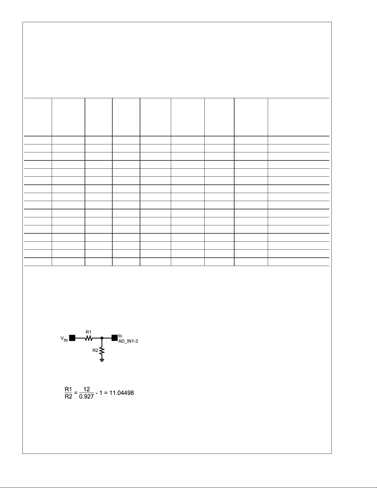
12.5 RECOMMENDED EXTERNAL SCALING RESISTORS FOR +12V POWER RAILS
The +12V inputs require external scaling resistors. The resistors need to scale 12V down to 0.927V.
Required External Scaling
Resistors for +12V Power Input
yields a ratio of 11.94498, which has a +0.27% deviation
from the theoretical. It is also recommended that the resis-
±
tors have
1% tolerance or better.
Each LSB in the voltage value registers has a weight of 12V
/ 192 = 62.5 mV. To calculate the actual voltage of the +12V
power input, use the following equation:
= (8-bit value register code) x (62.5 mV)
V
IN
12.6 RECOMMENDED EXTERNAL SCALING CIRCUIT
FOR −12V POWER INPUT
20068208
To calculate the required ratio of R1 to R2 use this equation:
The −12V input requires external resistors to level shift the
nominal input voltage of −12V to +0.309V.
It is recommended that the equivalent thevenin resistance of
the divider be between 1k and 7k to minimize errors caused
by leakage currents at extreme temperatures. The best values for the resistors are: R1=13.7 kΩ and R2=1.15 kΩ. This
www.national.com13
Page 14
12.0 Functional Description
LM93
(Continued)
Required External Level Shifting
Resistors for −12V Power Input
20068210
The +3.3V standby voltage is used as a reference for the
level shifting. Therefore, the tolerance of this voltage directly
effects the accuracy of the −12V reading. To minimize ratio
±
errors, a tolerance of better than
1% should be used. It is
recommended that the equivalent thevenin resistance of the
divider is between 1k and 7k to minimize errors caused by
leakage currents at extreme temperatures. To calculate the
ratio of R1 to R2 use this equation:
where VINis the nominal input voltage of −12V, V
reference voltage of +3.3V and AD_IN is the voltage required
at the AD input for a
1
⁄4scale reading or 0.309V.
Therefore, for this case:
Using standard 1% resistor values for R1 of 5.76 kΩ and R2
of 1.4 kΩ yields an R1 to R2 ratio of 4.1143.
The input voltage V
can be calculated using the value
IN
register reading (VR) using this equation:
The table below summarizes the theoretical voltage values
for value register readings near −12V.
Value Register V
IN
% ∆ from −12V
15 -13.2068 -10.0563
16 -13.1821 -9.8505
17 -13.1574 -9.6448
18 -13.1327 -9.4390
19 -13.1080 -9.2332
20 -13.0833 -9.0275
21 -13.0586 -8.8217
22 -13.0339 -8.6159
23 -13.0092 -8.4101
24 -12.9845 -8.2044
25 -12.9598 -7.9986
26 -12.9351 -7.7928
REF
is the
Value Register V
IN
27 -12.9104 -7.5871
28 -12.8858 -7.3813
29 -12.8611 -7.1755
30 -12.8364 -6.9698
31 -12.8117 -6.7640
32 -12.7870 -6.5582
33 -12.7623 -6.3524
34 -12.7376 -6.1467
35 -12.7129 -5.9409
36 -12.6882 -5.7351
37 -12.6635 -5.5294
38 -12.6388 -5.3236
39 -12.6141 -5.1178
40 -12.5894 -4.9121
41 -12.5648 -4.7063
42 -12.5401 -4.5005
43 -12.5154 -4.2947
44 -12.4907 -4.0890
45 -12.4660 -3.8832
46 -12.4413 -3.6774
47 -12.4166 -3.4717
48 -12.3919 -3.2659
49 -12.3672 -3.0601
50 -12.3425 -2.8544
51 -12.3178 -2.6486
52 -12.2931 -2.4428
53 -12.2684 -2.2370
54 -12.2438 -2.0313
55 -12.2191 -1.8255
56 -12.1944 -1.6197
57 -12.1697 -1.4140
58 -12.1450 -1.2082
59 -12.1203 -1.0024
60 -12.0956 -0.7967
61 -12.0709 -0.5909
62 -12.0462 -0.3851
63 -12.0215 -0.1793
64 -11.9968 0.0264
65 -11.9721 0.2322
66 -11.9474 0.4380
67 -11.9228 0.6437
68 -11.8981 0.8495
69 -11.8734 1.0553
70 -11.8487 1.2610
71 -11.8240 1.4668
72 -11.7993 1.6726
73 -11.7746 1.8784
74 -11.7499 2.0841
75 -11.7252 2.2899
76 -11.7005 2.4957
% ∆ from −12V
www.national.com 14
Page 15
12.0 Functional Description
(Continued)
Value Register V
IN
77 -11.6758 2.7014
78 -11.6511 2.9072
79 -11.6264 3.1130
80 -11.6018 3.3188
81 -11.5771 3.5245
82 -11.5524 3.7303
83 -11.5277 3.9361
84 -11.5030 4.1418
85 -11.4783 4.3476
86 -11.4536 4.5534
87 -11.4289 4.7591
88 -11.4042 4.9649
89 -11.3795 5.1707
90 -11.3548 5.3765
91 -11.3301 5.5822
92 -11.3054 5.7880
93 -11.2807 5.9938
94 -11.2561 6.1995
95 -11.2314 6.4053
96 -11.2067 6.6111
97 -11.1820 6.8168
98 -11.1573 7.0226
99 -11.1326 7.2284
100 -11.1079 7.4342
101 -11.0832 7.6399
102 -11.0585 7.8457
103 -11.0338 8.0515
104 -11.0091 8.2572
105 -10.9844 8.4630
106 -10.9597 8.6688
107 -10.9351 8.8745
108 -10.9104 9.0803
109 -10.8857 9.2861
110 -10.8610 9.4919
111 -10.8363 9.6976
112 -10.8116 9.9034
113 -10.7869 10.1092
12.7 DYNAMIC Vccp MONITORING USING VID
The AD_IN7 (CPU1 Vccp) and AD_IN8 (CPU2 Vccp) inputs
are dynamically monitored using the P1_VIDx and P2_VIDx
inputs to determine the limits. The dynamic comparisons
operate independently of the static comparisons which use
the statically programmed limits.
According to the VRM/VRD 10 specification when a VID
signal is ramping to a new value, it steps by one LSB at a
time, and one step occurs every 5 µs. In worse case, up to
20 steps may occur at once over 100 µs. The Vccp voltage
from the VRD has to settle to the new value within 50 µs of
the last VID change. The LM93 expects that the VID
changes will not occur more frequently than every 5 µs.
% ∆ from −12V
The VID signal can be changed by the processor under
program control, by internal thermal events or by external
control, like force PROCHOT.
The reference voltages selected by each value of the 6 bit
VID can be found in the VRM/VRD 10 spec. Transient VID
values caused by line-to-line skew are ignored by the LM93.
See the VRM/VRD 10 spec for the worst case line-to-line
skew.
The LM93 averages the VID values over a sampling window
to determine the average voltage that the VID input was
indicating during the sampling window. At the completion of a
voltage conversion cycle the LM93 performs limit comparisons based on average VID values and not instantaneous
values. The upper limit is determined by adding the upper
limit offset to the average voltage indicated by VID. The
lower limit is determined by subtracting the lower limit offset
from average voltage indicated by VID. If the AD_IN7 (or
AD_IN8) voltage falls outside the upper and lower limits, an
error event is generated. Dynamic and static comparisons
are performed once every 100 ms. The averaging time interval is 1.5 ms.
If at any time during the Vccp sampling window, the VID
code indicates that the VRD should turn off its output, the
dynamic Vccp checking is disabled for that sample.
±
The comparison accuracy is
25 mV, therefore the comparison limits must be set to include this error. Since the Vccp
voltage may be in the process of settling to a new value (due
to a VID change), this settling should be taken into account
when setting the upper and lower limit offsets.
The LM93 has a limitation on the upper limit voltage for
dynamic Vccp checking. The upper limit cannot exceed
1.5875V. If the sum of the voltage indicated by VID and the
upper offset voltage exceed 1.5875, the upper limit checking
is disabled.
12.8 V
V
REF
a voltage reference input for the BMC A/D inputs. V
2.5V
V
REF
OUTPUT
REF
is a fixed voltage to be used by an external VRD or as
±
1%. There is internal current limit protection for the
REF
output in case it gets shorted to supply or ground
accidentally.
12.9 PROCHOT BACKGROUND INFORMATION
PROCHOT is an output from a processor that indicates that
the processor has reached a predetermined temperature trip
point. At this trip point the processor can be programmed to
lower its internal operating frequency and/or lower its supply
voltage by changing the value of the 6 bit VID that it supplies
to the VRD. The final VID setting and the rate at which it
transitions to the new VID is programmable within the processor.
If PROCHOT is 100% throttled, it does not mean that the
CPU is not executing, but it may mean that the CPU is about
to encounter a thermal trip if the processor temperature
continues to rise.
PROCHOT is also an input to some processors so that an
external controller can force a thermal throttle based on
external events.
PROCHOT is no longer asserted by the processor when the
temperature drops below the predefined thermal trip point.
Oscillation around the trip point is avoided by the processor
by requiring that the temperature be above/below the trip
point for a predetermined period of time. A counter inside the
processor is used to track this time and it has to be incre-
LM93
is
www.national.com15
Page 16
12.0 Functional Description
LM93
(Continued)
mented to a max count for an above temperature trip and
decremented to zero when below the trip temperature setting, to remove the trip.
The minimum time for PROCHOT assertion is time dependant on the FSB frequency. The minimum time that the
processor asserts PROCHOT is estimated to be 187 µs.
12.10 PROCHOT MONITORING
PROCHOT monitoring applies to both the P1_PROCHOT
and P2_PROCHOT inputs. Both inputs are monitored in the
same fashion, but the following description discusses a
single monitor. (Px_PROCHOT represents both
P1_PROCHOT and P2_PROCHOT).
PROCHOT monitoring is meant to achieve two goals. One
goal is to measure the percentage of time that PROCHOT is
asserted over a programmable time period. The result of this
measurement can be read from an 8-bit register where one
LSB equals 1/256th of the PROCHOT Time Interval (0.39%).
The second goal is to have a status register that indicates,
as a coarse percentage, the amount of time a processor has
been throttled. This second goal is required in order to
communicate information over the NIC using ASF, i.e. status
can be sent, not values.
To achieve the first goal, the PROCHOT input is monitored
over a period of time as defined by the PROCHOT Time
Interval Register. At the end of each time period, the 8-bit
measurement is transferred to the Current Px_PROCHOT
register. Also at the end of each measurement period, the
Current Px_PROCHOT register value is moved to the Average Px_PROCHOT register by adding the new value to the
old value and dividing the result by 2. Note that the value that
is averaged into the Average Px_PROCHOT register is not
the new measurement but rather the previous measurement.
If the SMBus writes to the Current P1_PROCHOT (or Current P2_PROCHOT) register, the capture cycle restarts for
both monitoring channels (P1_PROCHOT and
P2_PROCHOT). Also note, that a strict average of two 8-bit
values may result in Average Px_PROCHOT reflecting a
value that is one LSB lower than the Current Px_PROCHOT
in steady state.
It should be noted that the 8-bit result has a positive bias of
one half of an LSB. This is necessary because a value of 00h
represents that Px_PROCHOT was not asserted at all during the sampling window. Any amount of throttling results in
a reading of 01h.
The following table demonstrates the mapping for the 8-bit
result:
8–Bit Result Percentage Thottled
0 Exactly 0%
1 Between 0% and 0.39%
2 Between 0.39% and 0.78%
AA
n Between (n-1)/256 and n/256
AA
253 Between 98.4% and 98.8%
254 Between 98.8% and 99.2%
255 Greater than 99.2%
To achieve the second goal, the LM93 has several comparators that compare the measured percentage reading against
several fixed and 1 variable value. The variable value is user
programmable.
The result of these comparisons generates several error
status bits described in the following table:
Status Description Comparison Formula
100% Throttle PROCHOT was never
de-asserted during
monitoring interval.
Greater than or equal to
75% and less than 100%
Greater than or equal to
50% and less than 75%
Greater than or equal to
25% and less than 50%
Greater than or equal to
12.5% and less than 25%
Greater than 0% and less
than 12.5%
Greater than 0% 0
Greater than user limit user limit
These status bits are reflected in the PROCHOT Error Status Registers. Each of the P1_PROCHOT and
P2_PROCHOT inputs is monitored independently, and each
has its own set of status registers.
In S3 and S4/5 sleep states, the PROCHOT Monitoring
function does not run. The Current Px_PROCHOT registers
are reset to 00h and the Average Px_PROCHOT registers
hold their current state. Once the sleep state changes back
to S0, the monitoring function is restarted. After the first
PROCHOT measurement has been made, the measurement is written directly into the Current and Average Px_PROCHOT registers without performing any averaging. Averaging returns to normal on the second measurement.
12.11 PROCHOT OUTPUT CONTROL
In some cases, it is necessary for the LM93 to drive the
Px_PROCHOT outputs low. There are several conditions
that cause this to happen.
The LM93 can be told to logically short the two PROCHOT
inputs together. When this is done, the LM93 monitors each
of the Px_PROCHOT inputs. If any external device asserts
one of the PROCHOT signals, the LM93 responds by asserting the other PROCHOT signal until the first PROCHOT
signal is de-asserted. This feature should never be enabled
if the PROCHOT signals are already being shorted by another means.
Whenever one of the VRDx_HOT inputs is asserted, the
corresponding Px_PROCHOT pins are asserted by the
LM93. The response time is less than 10 µs. When the
VRDx_HOT input is de-asserted, the Px_PROCHOT pin is
no longer asserted by the LM93. If the LM93 is configured to
short the PROCHOT signals together, it always asserts them
together whenever either of the VRDx_HOT inputs is asserted.
Software can manually program the LM93 to drive a PWM
type signal onto P1_PROCHOT or P2_PROCHOT. This is
done via the PROCHOT Override register. See the description of this register for more details. Once again, if the LM93
193 ≤ measured value and
not 100%
129 ≤ measured value
193
65 ≤ measured value
33 ≤ measured value<65
0<measured value<33
<
measured value
<
measured
value
<
<
129
www.national.com 16
Page 17

LM93
12.0 Functional Description
(Continued)
is configured to short the PROCHOT signals together, it
always asserts them together whenever this function is enabled.
12.12 FAN SPEED MEASUREMENT
The fan tach circuitry measures the period of the fan pulses
by enabling a counter for two periods of the fan tach signal.
The accumulated count is proportional to the fan tach period
and inversely proportional to the fan speed. All four fan tach
signals are measured within 1 second.
Fans in general do not over-speed if run from the correct
voltage, so the failure condition of interest is under speed
due to electrical or mechanical failure. For this reason only
low-speed limits are programmed into the limit registers for
the fans. It should be noted that, since fan period rather than
speed is being measured, a fan tach error event occurs
when the measurement exceeds the limit value.
12.13 SMART FAN SPEED MEASUREMENT
If a fan is driven using a low-side drive PWM, the tachometer
output of the fan is corrupted. The LM93 includes smart
tachometer circuitry that allows an accurate tachometer
reading to be achieved despite the signal corruption. In
smart tach mode all four signals are measured within 4
seconds.
A smart tach capture cycle works according to the following
steps:
1. Both PWM outputs are synchronized such that they
activate simultaneously.
2. Both PWM output active times are extended for up to 50
ms.
3. The number of tach signal periods during the 50 ms
interval are tracked:
a) If less than 1 period is sensed during the 50 ms exten-
sion the result returned is 3FFh.
b) After one period occurs the count for that period is
memorized.
c) If during the 50 ms interval 2 periods do not occur, the
tach value reported is the 1 period count multiplied by
2.
d) If 2 periods do occur, the 2 period count is loaded into
the value register and the 50 ms PWM extension is
terminated.
The lowest two bits in each of the Fan Tach value registers
are reserved. The smart tach feature takes advantage of
these bits. In normal tach mode, these bits return 00. In
smart tach mode the two bits determine the accuracy level of
the reading. 11 is most accurate (2 periods used) and 10 is
the least accurate (1 period used). If less than 1 period
occurred during the measurement cycle, the lower two bits
are set to 10.
In smart fan tach mode, the TACH_EDGE field is honored in
the LM93 Status/Control register. If only one edge type is
active, the measurement always uses that edge type (rising
or falling). If both are active, the measurement uses whichever edge type occurs first.
Typically the minimum RPM captured by smart fan tach
mode is 900 RPM for a fan that produces two pulses per
revolution at about 50% duty cycle.
13.0 Inputs/Outputs
Besides all the pins associated with sensor inputs the LM93
has several pins that are assigned for other specific functions.
13.1 ALERT OUTPUT
The ALERT output is an active-low open drain output signal.
The ALERT output is used to signal a micro-controller that
one or more sensors have crossed their corresponding limit
thresholds. This is generally not a fatal event unless the
micro-controller decides it to be.
If enabled, the ALERT output is asserted whenever any bit in
any BMC Error Status register is set (with the exception of
the fixed PROCHOT threshold bits). By definition, when
ALERT is enabled, it always matches the inverse of the
BMC_ERR bit in the LM93 Status/Control register. When the
ALERT output is disabled, an alert event can still be determined by reading the state of the BMC_ERR bit.
The ALERT functions like an interrupt. The LM93 does not
support the SMBus ARA (Alert Response Address) protocol.
ALERT is only de-asserted when there are no error status
bits set in any BMC Error Status registers. Alternatively,
software can disable the ALERT output to cause it to deassert. The ALERT output re-asserts once enabled if any
BMC Error Status register bits are still set.
Further information on how the ALERT output behaves can
be found in Section 15.7 MASKING, ERROR STATUS AND
ALERT.
13.2 RESET INPUT/OUTPUT
This pin acts as an active low reset output when power is
applied to the LM93. It is asserted when the LM93 first sees
a voltage that exceeds the internal POR level on its +3.3V
S/B V
their defaults when power is applied.
After this reset has completed, the RESET pin becomes an
input. When an external device asserts RESET, the LM93
clears the LOCK bit in the LM93 Configuration register. This
feature allows critical registers to be locked and provides a
controlled mechanism to unlock them.
Asserting RESET externally causes the Sleep State Control
register to be automatically set to S4/5. This causes several
error events to be masked according to the S4/5 masking
definitions. Refer to the register descriptions for more information.
13.3 PWM1 AND PWM2 OUTPUTS
The PWM outputs are used to control the speed of fans. The
output signal duty cycle can automatically be controlled by
the temperature of one or more temperature zones. It is also
influenced by various other inputs and registers. See Section
15.10 FAN CONTROL for further information on the behavior
of the PWM outputs.
13.4 SCSI_TERMx INPUTS
These inputs can be used to monitor the status of the
electronic fuse on each of the SCSI channels. In prior implementations the reference voltage out to the terminators was
measured. When LVDS SCSI was introduced this reference
voltage could take on multiple voltage levels depending on
the mode of the SCSI bus. Also when the SCSI terminators
were disabled, the V
Monitoring individual terminators was also pin intensive. All
input. The internal registers of the LM93 are reset to
DD
voltage could not be guaranteed.
REF
www.national.com17
Page 18

13.0 Inputs/Outputs (Continued)
LM93
of these issues caused problems that were difficult to work
around so moving to monitoring the fuse was selected as the
solution.
These inputs do not have to be used for monitoring SCSI
fuses. Assertion of the SCSI_TERMx inputs to a Low sets
the associated bits the status registers. Therefore, any active
low signal could be connected to these pins to generate an
error event.
13.5 VRD1_HOT AND VRD2_HOT INPUTS
These inputs monitor the thermal sensor associated with
each processor VRD on a baseboard. When one of the
inputs is activated, it indicates that the VRD has exceeded a
predetermined temperature threshold. The LM93 responds
by gradually increasing the duty cycle of any PWM outputs
that are bound to the corresponding processor and setting
the appropriate error status bits. The corresponding
PROCHOT signal is also asserted. See the Section 15.10
FAN CONTROL and the Section 12.11 PROCHOT OUTPUT
CONTROL for more information.
13.6 GPIO PINS
The LM93 has 8 GPIO pins than can act as either as inputs
or outputs. Each can be configured and controlled independently. When acting as an input the pin can be masked to
prevent it from setting a corresponding bit in the GPI Error
status registers.
13.7 FAN TACH INPUTS
The fan inputs are Schmitt-Trigger digital inputs. Schmitttrigger input circuitry is included to accommodate slow rise
and fall times typical of fan tachometer outputs.
The maximum input signal range is 0V to +6.0V, even when
is less than 5V. In the event that these inputs are
V
DD
supplied from fan outputs, which exceed 0V to +6.0V, either
resistive attenuation of the fan signal or diode clamping must
be included to keep inputs within an acceptable range,
thereby preventing damage to the LM93.
Hot plugging fans can involve spikes on the Tach signals of
up to 12V so diode protection or other circuitry is required.
For “Hot Plug” fans, external clamp diodes may be required
for signal conditioning.
14.0 SMBus Interface
The SMBus is used to communicate with the LM93. The
LM93 provides the means to monitor power supplies for fan
status and power failures. LM93 is designed to be tolerant to
5V signalling. Necessary pull-ups are located on the baseboard. Care should be taken to ensure that only one pull-up
is used for each SMBus signal. For proper operation, the
SMBus slave addresses of all devices attached to the bus
must comply with those listed in this document. The SMBus
interface obeys the SMBus 2.0 protocols and signaling levels.
The SMBus interface of the LM93 does not load down the
SMBus if no power is applied to the LM93. This allows a
module containing the LM93 to be powered down and replaced, if necessary.
14.1 SMBUS ADDRESSING
Each time the LM93 is powered up, it latches the assigned
SMBus slave address (determined by ADDR_SEL) during
the first valid SMBus transaction in which the first five bits of
the targeted slave address match those of the LM93 slave
address. Once the address has been latched, the LM93
continues to use that address for all future transactions until
power is lost.
The address select input detects three different voltage levels and allows for up to 3 devices to exist in a system. The
address assignment is as follows:
Address Select Pin
(ADDR_SEL)
High 01011 01
V
/2 01011 10
DD
Low 01011 00
14.2 DIGITAL NOISE EFFECT ON SMBUS COMMUNICATION
Noise coupling into the digital lines (greater than 150mV),
overshoot greater than V
may prevent successful SMBus communication with the
LM93. SMBus No Acknowledge (NACK) is the most common symptom, causing unnecessary traffic on the bus. Although, the SMBus maximum frequency of communication is
rather low (100 kHz max), care still needs to be taken to
ensure proper termination within a system with multiple parts
on the bus and long printed circuit board traces. The LM93
includes on chip low-pass filtering of the SMBCLK and SMBDAT signals to make it more noise immune. Minimize noise
coupling by keeping digital traces out of switching baseboard
areas as well as ensuring that digital lines containing high
speed data communications cross at right angles to the
SMBDAT and SMBCLK lines.
14.3 GENERAL SMBUS TIMING
The SMBus 2.0 specification defines specific conditions for
different types of read and write operations but in general the
SMBus protocol operates as follows:
The master initiates data transfer by establishing a START
condition, defined as a high to low transition on the serial
data line SMBDAT while the serial clock line SMBCLK remains high. This indicates that a data stream follows. All
slave peripherals connected to the serial bus respond to the
START condition, and shift in the next 8 bits. This consists of
a 7-bit slave address (MSB first) plus a R/W bit, which
determines the direction of the data transfer, i.e. whether
data is written to or read from the slave device (0 = write, 1
= read).
The peripheral whose address corresponds to the transmitted address responds by pulling the data line low during the
low period before the ninth clock pulse, known as the Acknowledge Bit, and holding it low during the high period of
this clock pulse. All other devices on the bus now remain idle
while the selected device waits for data to be read from or
written to it. If the R/W bit is a 0 then the master writes to the
slave device. If the R/W bit is a 1 the master reads from the
slave device.
Data is sent over the serial bus in sequences of 9 clock
pulses, 8 bits of data followed by an Acknowledge bit. Data
transitions on the data line must occur during the low period
of the clock signal and remain stable during the high period,
as a low to high transition when the clock is high may be
interpreted as a STOP signal.
If the operation is a write operation, the first data byte after
the slave address is a command byte. This tells the slave
device what to expect next. It may be an instruction, such as
and undershoot less than GND,
DD
Slave Address
Assignment
www.national.com 18
Page 19

14.0 SMBus Interface (Continued)
telling the slave device to expect a block write, or it may
simply be a register address that tells the slave where subsequent data is to be written.
Since data can flow in only one direction as defined by the
R/W bit, it is not possible to send a command to a slave
device during a read operation. Before doing a read operation, it is necessary to do a write operation to tell the slave
what sort of read operation to expect and/or the address
from which data is to be read.
When all data bytes have been read or written, stop conditions are established. In WRITE mode, the master will allow
the data line to go high during the 10th clock pulse to assert
a STOP condition. In READ mode, the slave drives the data
not the master. For the bit in question, the slave is looking for
an acknowledge and the master doesn’t drive low. This is
known as ‘No Acknowledge’. The master then takes the data
line low during the low period before the 10th clock pulse,
then high during the 10th clock pulse to assert a STOP
condition.
Note, a repeated START may be given only between a write
and read operation that are in succession.
14.4 SMBUS ERROR SAFETY FEATURES
To provide a more robust SMBus interface, the LM93 incorporates a timeout feature for both SMBCLK and SMBDAT. If
either signal is low for a long period of time (see SMBus AC
specs), the LM93 SMBus state machine reverts to the idle
state and waits for a START signal. Large block transfers of
all zeros should be avoided if the SMBCLK is operating at a
very low frequency to avoid accidental timeouts. Pulling the
Reset pin low does not reset the SMBus state machine. If the
LM93 SMBDAT pin is low during a system reset, the LM93’s
state machine timeouts and resets automatically. If the
LM93’s SMBDAT pin is high during a system reset, the first
assertion of a start by the master resets the LM93’s interface
state machine.
Although it is a violation of the SMBus specification, in some
cases a START or STOP signal occurs in the middle of a
byte transfer instead of coming after an acknowledge bit. If
this occurs, only a partial byte was transferred. If a byte was
being written, it is aborted and the partial byte is not committed. If a byte was being read from a read-to-clear register,
the register is not cleared.
14.5 SERIAL INTERFACE PROTOCOLS
The LM93 contains volatile registers, the registers occupy
address locations from 00h to EFh.
Data can be read and written as a single byte, a word, or as
a block of several bytes. The LM93 supports the following
SMBus/I
2
C transactions/protocols:
— Send Byte
— Write Byte
— Write Word
— SMBus Write Block
2
—I
C Block Write
— Read Byte
— Read Word
— SMBus Read Block
— SMBus Block-Write Block-Read Process Call
2
C Block Read
—I
In addition to these transactions the LM93 supports a few
extra items and also has some behavior that must be defined
beyond the SMBus 2.0 specification. No other SMBus 2.0
transactions are supported (PEC, ARA etc.).
The SMBus specification defines several protocols for different types of read and write operations. The ones used in the
LM93 are discussed below. The following abbreviations are
used in the diagrams:
S — START
P — STOP
R — READ
W — WRITE
A — ACKNOWLEDGE
/A — NO ACKNOWLEDGE
14.5.1 Address Incrementing
The established base address does not increment. Repeatedly reading without re-establishing a new base address
returns data from the same address each time. I
2
C read
transactions can use this information and skip reestablishing
the base address, when only one master is used. One
exception to this rule exists when a block write and block
read is used to emulate a block write/read process call. This
is detailed later, see the Block Write/Read Process Call
description.
LM93
www.national.com19
Page 20
14.0 SMBus Interface (Continued)
LM93
14.5.2 Block Command Code Summary
Block command codes control the block read and write operations of the LM93 as summarized in the following table:
Command Code Name Value Description
Block Write Command F0h SMBus Block Write Command Code
Block Read Command F1h SMBus Block Write/Read Process Call
Fixed Block 0 F2h Fixed Block Read Command Code: address 40h, size 8 bytes
Fixed Block 1 F3h Fixed Block Read Command Code: address 48h, size 8 bytes
Fixed Block 2 F4h Fixed Block Read Command Code: address 50h, size 6 bytes
Fixed Block 3 F5h Fixed Block Read Command Code: address 56h, size 16 bytes
Fixed Block 4 F6h Fixed Block Read Command Code: address 67h, size 4 bytes
Fixed Block 5 F7h Fixed Block Read Command Code: address 6Eh, size 8 bytes
Fixed Block 6 F8h Fixed Block Read Command Code: address 78h, size 12 bytes
Fixed Block 7 F9h Fixed Block Read Command Code: address 90h, size 32 bytes
Fixed Block 8 FAh Fixed Block Read Command Code: address B4h, size 8 bytes
Fixed Block 9 FBh Fixed Block Read Command Code: address C8h, size 8 bytes
Fixed Block 10 FCh Fixed Block Read Command Code: address D00h, size 16 bytes
Fixed Block 11 FDh Fixed Block Read Command Code: address E5h, size 9 bytes
14.5.3 Write Operations
The LM93 supports the following SMBus write protocols.
14.5.3.1 Write Byte
In this operation the master device sends an address byte and one data byte to the slave device, as follows:
1. The master device asserts a START condition.
2. The master sends the 7-bit slave address followed by the write bit (low).
3. The addressed slave device asserts ACK.
4. The master sends a command code (register address).
5. The slave asserts ACK.
6. The master sends the data byte.
7. The slave asserts ACK.
8. The master asserts a STOP condition to end the transaction.
12 34 5678
S Slave
Address
W A Register
Address
A Data
Byte
AP
14.5.3.2 Write Word
In this operation the master device sends an address byte and two data bytes to the slave device, as follows:
1. The master device asserts a START condition.
2. The master sends the 7-bit slave address followed by the write bit (low).
3. The addressed slave device asserts ACK.
4. The master sends a command code (register address).
5. The slave asserts ACK.
6. The master sends the low data byte.
7. The slave asserts ACK.
8. The master sends the high data byte.
9. The slave asserts ACK.
10. The master asserts a STOP condition to end the transaction.
12 34 56 78 910
S Slave
Address
www.national.com 20
W A Register
Address
A Data Byte
Low
A Data Byte
High
AP
Page 21
14.0 SMBus Interface (Continued)
14.5.3.3 SMBus Write Block to Any Address
The start address for a block write is embedded in this transaction. In this operation the master sends a block of data to the slave
as follows:
1. The master device asserts a START condition.
2. The master sends the 7-bit slave address followed by the write bit (low).
3. The addressed slave device asserts ACK.
4. The master sends a command code that tells the slave device to expect a block write. The LM93 command code for a block
write is F0h.
5. The slave asserts ACK.
6. The master sends a byte that tells the slave device how many data bytes it will send (N). The SMBus specification allows a
maximum of 32 data bytes to be sent in a block write.
7. The slave asserts ACK.
8. The master sends data byte 1, the starting address of the block write.
9. The slave asserts ACK after each data byte.
10. The master sends data byte 2.
11. The slave asserts ACK.
12. The master continues to send data bytes and the slave asserts ACK for each byte.
13. The master asserts a STOP condition to end the transaction.
12 34 56 78 910 11A12 13
S Slave
Address
W A Command
F0h
(Block
Write)
A Byte
Count
(N)
A Data
Byte 1
(Start
Address)
A Data
Byte 2
A
A
Data
Byte N
AP
LM93
Special Notes
1. Any attempts to write to bytes beyond normal address space are acknowledged by the LM93 but are ignored.
2. Block writes do not wrap from address FFh back to 00h the address remains at FFh.
3. The Byte Count field is ignored by the LM93. The master device may send more or less bytes and the LM93 accepts them.
4. The SMBus specification requires that block writes never exceed 32 data bytes. Meeting this requirement means that only 31
actual data bytes can be sent (the register address counts as one byte). The LM93 does not care if this requirement is met.
2
14.5.3.4 I
In this transaction the master sends a block of data to the LM93 as follows:
1. The master device asserts a START condition.
2. The master sends the 7-bit slave address followed by the write bit (low).
3. The addressed slave device asserts ACK.
4. The master sends the starting address of the block write.
5. The slave asserts ACK after each data byte.
6. The master sends data byte 1.
7. The slave asserts ACK.
8. The master continues to send data bytes and the slave asserts ACK for each byte.
9. The master asserts a STOP condition to end the transaction
Special Notes:
1. Any attempts to write to bytes beyond normal address space are acknowledged by the LM93 but are ignored.
2. Block writes do not wrap from address FFh back to 00h the address remains at FFh.
C™Block Write
12 34 56 7 8 9
S Slave
Address
W A Register
Address
A Data
Byte 1
A
A
Data
Byte N
AP
www.national.com21
Page 22

14.0 SMBus Interface (Continued)
LM93
14.5.4 Read Operations
The LM93 uses the following SMBus read protocols.
14.5.4.1 Read Byte
In the LM93, the read byte protocol is used to read a single byte of data from a register. In this operation the master device
receives a single byte from a slave device, as follows:
1. The master device asserts a START condition.
2. The master sends the 7-bit slave address followed by the write bit (low).
3. The addressed slave device asserts ACK.
4. The master sends a register address.
5. The slave asserts an ACK.
6. The master sends a Repeated START.
7. The master sends the slave address followed by the read bit (high).
8. The slave asserts an ACK.
9. The master receives a data byte and asserts a NACK.
10. The master asserts a STOP condition and the transaction ends.
12 34 567 89 10
S Slave
Address
14.5.4.2 Read Word
In the LM93, the read word protocol is used to read two bytes of data from a register or two consecutive registers. In this operation
the master device reads two bytes from a slave device, as follows:
1. The master device asserts a START condition.
2. The master sends the 7-bit slave address followed by the write bit (low).
3. The addressed slave device asserts ACK.
4. The master sends a register address.
5. The slave asserts an ACK.
6. The master sends a Repeated START.
7. The master sends the slave address followed by the read bit (high).
8. The slave asserts an ACK.
9. The master receives the Low data byte and asserts an ACK.
10. The master receives the High data byte and asserts a NACK.
11. The master asserts a STOP condition and the transaction ends.
12 34 567 89 10 11
S Slave
Address
W A Register
W A Register
Address
A S Slave
Address
A S Slave
Address
R A Data
Address
R A Data
Byte
Byte Low
A Data
Byte High
/A P
/A P
14.5.4.3 SMBus Block-Write Block-Read Process Call
This transaction is used to read a block of data from the LM93. Below is the sequence of events that occur in this transaction:
1. The master device asserts a START condition.
2. The master sends the 7-bit slave address followed by the write bit (low).
3. The addressed slave device asserts ACK.
4. The master sends a command code that tells the slave device to expect a block read (F1h) and the slave asserts ACK.
5. The master sends the Byte Count for this write which is 2 and the slave asserts ACK.
6. The master sends the Start Register Address for the block read and the slave asserts the ACK.
7. The master sends the Byte Count (1-32) for the block read processes call and the slave asserts ACK.
8. The master asserts a repeat START condition.
9. The master sends the 7-bit slave address followed by the read bit (high).
10. The slave asserts ACK.
11. The master receives a byte count data byte that tells it how many data bytes will received. This field reflects the number of
bytes requested by the Byte Count transmitted to the LM93. The SMBus specification allows a maximum of 32 data bytes to
be received in a block read. Then master asserts ACK.
www.national.com 22
Page 23

14.0 SMBus Interface (Continued)
12. The master receives byte 1 and then asserts ACK.
13. The master receives byte 2 and then asserts ACK.
14. The master receives N-3 data bytes, and asserts ACK for each one.
15. The master receives data byte N and asserts a NACK.
16. The master asserts a STOP condition to end the transaction.
12345678910
S Slave
Address
Special Notes:
1. The LM93 returns 00h when address locations outside of normal address space are read.
2. Block reads do not wrap around from address FFh to 00h
3. If the master acknowledges more bytes that it requested, the LM93 continues to supply data until the master does not
acknowledge a byte.
4. If the master does not acknowledges a byte to prematurely abort a block read, the LM93 gets off the bus to allow the master
to issue a STOP signal.
W A Block
Read
Command
Code
(F1h)
11 12 13 14 15 15 16
A
Byte
Count
(1–20h)
(N)
A Byte
A Data
Byte 1
Count
(2h)
A Start
Register
Address
A Data
Byte 2
A Byte
Count
(1–20h)
(N)
A
A S Slave
A
Data
Byte N
Address
/A P
RA
A
LM93
www.national.com23
Page 24

14.0 SMBus Interface (Continued)
LM93
14.5.4.4 Simulated SMBus Block-Write Block-Read Process Call
Alternatively, if the master cannot support an SMBus Block-Write Block-Read process call, it can be emulated by two transactions
(a block write followed by a block read). This should only be done in a single master system, since in a dual master system
collisions can occur that corrupt the data and transaction. Below is the sequence of events for these transactions:
1. The master issues a START to start this transaction.
2. The master sends the 7-bit slave address followed by a write bit (low).
3. The slave asserts the ACK.
4. The master sends the Block Read command code (F1h) and the slave asserts the ACK.
5. The master sends the Byte Count (2h) for this transaction and the slave asserts the ACK.
6. The master sends the Start Register Address and the slave asserts the ACK.
7. The master sends the Byte Count (1-20h) for the Block-Read Process Call and the slave asserts the ACK.
8. The master sends a STOP to end this transaction.
9. The master sends a START to start this transaction.
10. The master sends the 7-bit slave address followed by a write bit (low) and the slave asserts the ACK.
11. The master sends the Block Read Command code (F1h) and the slave asserts the ACK.
12. The master sends a repeat START.
13. The master sends the 7-bit slave address followed by a read bit (high) and the slave asserts the ACK.
14. The master receives Byte Count (this matches the size sent by the master in step 7) and asserts the ACK.
15. The master receives Data Byte 1 and asserts the ACK.
16. The master receives Data Byte 2 and asserts the ACK.
17. The master receives N-3 data bytes, and asserts ACK for each one.
18. The master receives the last data byte and asserts a NACK.
19. The master issues a STOP to end this transaction.
12345678910
S Slave
Address
W A Block
Read
Command
Code
(F1h)
A Byte
Count
(2h)
A Start
Register
Address
A Byte
Count
(1–20h)
(N)
A P S Slave
Address
WA
A
11 12 13 14 15 16 17 16
A
Block
Read
Command
Code
(F1h)
Special Notes:
1. Steps 9 through 19 can be repeated to read another block of data. The address auto-increments such that the next block
starts where the last block left off. The size returned by the LM93 is the same each time.
2. The LM93 returns 00h when address locations outside of normal address space are read.
3. Block reads do not wrap around from address FFh to 00h
4. If the master acknowledges more bytes that it requested, the LM93 continues to supply data until the master does not
acknowledge a byte.
5. If the master does not acknowledges a byte to prematurely abort a block read, the LM93 gets off the bus to allow the master
to issue a STOP signal.
6. After a block read is finished, the base address of the LM93 is updated to point to the byte just beyond the last byte read.
14.5.4.5 SMBus Fixed Address Block Reads
Block reads can be performed from pre-defined addresses. A special command code has been reserved for each pre-defined
address. See the Section 14.5.2 Block Command Code Summary for more details on the command codes. Below is the
sequence of events that occur for this type of block read:
1. The master sends a START to start this transaction.
2. The master sends the 7-bit slave address followed by a write bit (low).
3. The slave asserts an ACK.
4. The master sends a Fixed Block Command Code (F2h-FDh) and the slave asserts an ACK.
A S Slave
Address
R A Byte
Count
(1–20h)
(N)
A Data
Byte 1
A Data
Byte 2
A
A
Data
Byte N
/A P
www.national.com 24
Page 25
14.0 SMBus Interface (Continued)
5. The master sends a repeated START.
6. The master sends the 7-bit slave address followed by a read bit (high).
7. The slave asserts an ACK.
8. The master receives the Byte Count (depends on the Fixed Block Command Code used) and asserts an ACK.
9. The master receives the first data byte and asserts an ACK.
10. The master continues to receive data bytes and asserting an ACK.
11. The master receives the last data byte.
12. The master asserts a NACK.
13. The master issues a STOP to end this transaction.
12 34 56 78 9 1011 1213
S Slave
Address
W A Fixed
Block
Command
A S Slave
Address
R A Byte
Count
(N)
A Data
Byte 1
Code
(F2h–FDh)
Special Notes:
1. The LM93 returns 00h when address locations outside of normal address space are read.
2. Block reads do not wrap around from address FFh to 00h.
3. If the master acknowledges more bytes that it requested, the LM93 continues to supply data until the master does not
acknowledge a byte.
4. If the master does not acknowledges a byte to prematurely abort a block read, the LM93 gets off the bus to allow the master
to issue a STOP signal.
2
14.5.4.6 I
The LM93 supports I
C Block Reads
2
C block reads. The following sequence of events occur in this transaction:
1. The master sends a START to start this transaction .
2. The master send 7-bit slave address followed by a write bit (low).
3. The slave asserts an ACK.
4. The master sends the register address and the slave asserts an ACK.
5. The master sends a repeated START.
6. The master sends the 7-bit slave address followed by a read bit (high).
7. The slave asserts an ACK.
8. The master receives Data Byte 1 and asserts an ACK.
9. The master continues to receive bytes and asserting an ACK for each byte received.
10. The master receives the last byte.
11. The master asserts a NACK.
12. The master issues a STOP.
12 34 56 78 9
S Slave
Address
W A Register
Address
A S Slave
Address
R A Data
Byte 1
A Data
Byte 2
A
A
Data
/A P
Byte N
A
10 11 12
A
A
Data
/A P
Byte N
LM93
Special Notes:
1. The LM93 returns 00h when address locations outside of normal address space are read.
2. Block reads do not wrap around from address FFh to 00h.
3. If the master acknowledges more bytes that it requested, the LM93 continues to supply data until the master does not
acknowledge a byte.
4. If the master does not acknowledges a byte to prematurely abort a block read, the LM93 gets off the bus to allow the master
to issue a STOP signal.
14.6 READING AND WRITING 16-BIT REGISTERS
Whenever the low byte of a 16-bit register is read, the high
byte is frozen. After the high byte is read, it is unfrozen. This
ensures that the entire 16-bit value is read properly and the
high byte matches with the low byte. If the low byte of a
different 16-bit register is read, the currently frozen high byte
is unfrozen and the high byte of the new 16-bit register is
frozen. In a system with two SMBus masters, it is very
important that only one master reads any 16-bit registers at
a time. One possible method to achieve this would involve
using 16-bit SMBus reads (instead of two separate 8-bit
reads) to read 16-bit registers.
www.national.com25
Page 26
14.0 SMBus Interface (Continued)
LM93
Whenever the low byte of a 16-bit register is written, the write
is buffered and does not take effect until the corresponding
high byte is written. If the low byte of a different 16-bit
register is written, the previously buffered low byte of the first
register is discarded. If a device attempts to write the high
byte of a 16-bit register, and the corresponding low byte was
not written (or was discarded), then the LM93 will NACK the
byte.
15.0 Using The LM93
15.1 POWER ON
The LM93 generates a power on reset signal on RESET
when power is applied for the first time to the part.
15.2 RESETS
Upon power up, the RESET output is asserted when the
voltage on the power supply crosses the power-on-reset
threshold level (see Electrical Specifications). The RESET
output is open-drain and should be used with an external
pull-up resistor connected to V
has completed, the RESET pin becomes an input and when
asserted causes the LOCK bit in the LM93 Configuration
register to be cleared. In addition, assertion of RESET
causes the sleep control register to be automatically set to
S4/S5. This causes several error events to be masked according to the S4/S5 masking definitions.
Register Types
Factory regs x
. Once the power on reset
DD
Power
On Reset
External
Reset
Register Types
Power
On Reset
External
Reset
BMC Error Status regs x
Host Error Status regs x
Value regs
Limit regs x
Setup regs x
LM93 Configuration Lock Bit x x
LM93 Configuration GMSK Bit x (reset) x (set)
Sleep Mask x
Sleep State Control x
Other Mask regs x
All other registers are not effected by power on reset or
external reset.
15.3 ADDRESS SELECTION
LM93 is designed to be used primarily in dual processor
server systems that may require only one monitoring device.
If multiple LM93 devices are implemented in a system, they
must have unique SMBus slave addresses. See the Section
14.1 SMBUS ADDRESSING for more information.
The board designer may apply a 10 kΩ pull-down and/or
pull-up resistors to ground and/or to 3.3V SB V
DD
on the
ADDR_SEL pin. The LM93 is designed to work with resistors
of 5% tolerance for the case where two resistors are required. Upon the first SMBus communication to the part, the
LM93 assigns itself an SMBus address according to the
ADDR_SEL input.
Address Select Board Implementation SMBus Address
less-than 10% of V
≈ V
/2 10 kΩ (5%) Resistor to 3.3V SB VDDand to Ground 0101,110b
DD
greater-than 90% of V
DD
DD
Pulled to ground through a 10 kΩ resistor 0101,100b
Pulled to 3.3V SB VDDthrough a 10 kΩ resistor 0101,101b
15.4 DEVICE SETUP
BIOS executes the following steps to configure the registers
in the LM93. All steps may not be necessary if default values
are acceptable.
Set limits and parameters (not necessarily in this order):
Set up Fan control
Set up PWM temperature bindings
Set fan tach limits
Set fan boost temperature and hysteresis
Set the VRD_HOT and PROCHOT PWM ramp control
Set voltage sensor limits and hysteresis
Set the Dynamic Vccp offset limits
Set the Sleep State control and mask registers
Set Other Mask Registers (GPI Error, VRDx_HOT, SC-
SI_TERM, and dynamic Vccp limit checking)
Set start bit to select user values and unmask error events
Set the sleep state to 0
Set Lock bit to lock the limit and parameter registers
(optional)
rate
Enable Smart Tach Mode and Tachometer Input to PWM
binding (required with direct PWM drive of fans)
Set the temperature absolute limits
Set the temperature hysteresis values
Set temperature filtered or unfiltered usage
Set the Zone Adjustment Offset temperature
Set the PROCHOT override and time interval values
15.5 ROUND ROBIN VOLTAGE/TEMPERATURE CONVERSION CYCLE
The LM93 monitoring function is started as soon as the part
is powered up. The LM93 performs a “round robin” sampling
of the inputs, in the order shown below. Each cycle of the
round robin is completed in less than 100 ms.
The results of the sampling and conversions can be found in
the value registers and are available at any time.
Set the PROCHOT user limit
Enable THERMTRIP masking of error events (if GPIO4
and GPIO5 are used as THERMTRIP inputs)
www.national.com 26
Page 27
15.0 Using The LM93 (Continued)
Channel
#
1 Temp Zone 1 Remote Diode 1 Temp
2 Temp Zone 2 Remote Diode 2 Temp
3 Temp Zone 3 Internal Temperature
4 AIN1 +12V1
5 AIN2 +12V2
6 AIN3 +12V3
7 AIN4 FSB_Vtt
8 AIN5 3GIO/PXH/MCH_Core
9 AIN6 ICH_Core
10 AIN7 CPU_1Vccp
11 AIN8 CPU2_Vccp
12 AIN9 3.3V
13 AIN10 +5V
14 AIN11 SCSI_Core
15 AIN12 Mem_Core
16 AIN13 Mem_Vtt
17 AIN14 GBIT_Core
18 AIN15 −12V
19 AIN16 3.3V SB V
15.6 ERROR STATUS REGISTERS
The LM93 contains several error status registers for the
BMC side, and duplicated error status registers for the Host
side. These registers are used to reflect the state of all the
possible error conditions that the LM93 monitors.
The BMC/Host Error Status registers hold a set bit until the
event is cleared by software, even if the condition causing
the error event goes away.
To clear a bit in the Error Status registers, a ‘1’ has to be
written to the specific bit that is required to be cleared. If the
event that caused the error is no longer active then the bit is
cleared.
Clearing a bit in a BMC Error Status register does not clear
the corresponding bit in the Host Error Status register or vise
versa.
15.6.1 ASF Mode
In order for the LM93 part to act as a legacy sensor (6.1.2 of
ASF spec DSP0114 rev 2) and to easily bolt up to the SMBus
of an ASF capable NIC chip, the treatment of the Error
Status registers needs to change.
The LM93 can be placed into ASF mode by setting the
appropriate bit in the LM93 Status/Control register. Once this
bit is set, the BMC Error Status registers become read-toclear. Writing a ‘1’ to clear a particular bit is also allowed in
ASF mode. The Host Error Status registers are not effected
by ASF mode.
Input Typical Assignment
Reading
Reading
Reading
Supply Rail
DD
LM93
15.7 MASKING, ERROR STATUS AND ALERT
Masking is always applied to bits in the HOST and BMC
Error Status registers. If an event is masked, the corresponding error bit in the HOST or BMC Error Status registers
is prevented from ever being set. As a result, this prevents
the event from ever causing ALERT to be asserted. Masking
an event does not clear its associated Error Status bit if it is
currently set.
Voltage errors are masked by writing a high voltage limit
value of FFh. This is the default high limit for all voltages.
Temperature errors are masked by writing a high temperature limit value of 80h. This is the default high limit for all
temperatures. Masking a temperature channel masks both
temperature errors and diode fault errors.
The GPI Mask register allows GPI errors to be masked. Any
bits that are set in this register mask events for the corresponding GPIO_x pin.
User PROCHOT status is not really an error but it can be
used to notify the user of processor throttling past a preset
USER limit. A user limit of FFh acts as the mask for this
register. Error bits associated with the predefined
PROCHOT thresholds cannot be masked. It is important to
note though, that these error bits do not cause BMC_ERR,
HOST_ERR, or ALERT to be asserted under any condition.
Fan tach errors are masked if the tach limit for the given tach
is set to FFh .
SCSI_TERMx errors and VRDx_HOT errors can be masked
by setting the appropriate bit in the VRD THERMTRIP and
SCSI_TERM Error Mask register.
When the LM93 powers up, the ALERT output is disabled.
The ALERT output can be enabled by setting the ALERT_EN
bit in the LM93 Configuration register.
In addition the manual masking options, the LM93 also
masks some errors depending on the sleep state of the
system. The sleep state of the system is communicated to
the LM93 by writing to the Sleep State Control register.
Some types of error events are always masked in certain
sleep modes. Some types of error events are optionally
masked in certain sleep modes if their sleep mask register
bit is set. Refer to the register descriptions for more information.
15.8 LAYOUT AND GROUNDING
Analog components such as voltage dividers should be
physically located as close as possible to the LM93.
The LM93 bypass capacitors, the parallel combination of
100 pF, 10 µF (electrolytic or tantalum) and 0.1 µF (ceramic)
bypass capacitors must be connected between power pin
(pin 39) and ground, and should be located as close as
possible to the LM93. The 100 pF capacitor should be
placed closest to the power pin.
15.9 THERMAL DIODE APPLICATION
To measure temperature external to the LM93, we need to
use a remote discrete diode to sense the temperature of
external objects or ambient air. Remember that the temperature of a discrete diode is effected, and often dominated, by
the temperature of its leads.
Most silicon diodes do not lend themselves well to this
application. It is recommended that a MMBT3904 transistor
type base emitter junction be used with the collector tied to
the base.
www.national.com27
Page 28
15.0 Using The LM93 (Continued)
LM93
Thermal Diode Temperature vs. LM93 Temperature
Reading
15.9.1 Accuracy Effects of Diode Non-Ideality Factor
The technique used in today’s remote temperature sensors
is to measure the change in V
at two different operating
BE
points of a diode. For a bias current ratio of N:1, this difference is given as:
20068215
15.9.2 PCB Layout for Minimizing Noise
In the following guidelines, D+ and D− refer to the REMOTE1+, REMOTE1−, REMOTE2+, REMOTE2− pins.
In a noisy environment, such as a power supply, layout
considerations are very critical. Noise induced on traces
running between the remote temperature diode sensor and
the LM93 can cause temperature conversion errors.
The following guidelines should be followed:
1. Place a 0.1 µF and 100 pF LM93 power bypass capaci-
tors as close as possible to the V
pin, with the 100pF
DD
capacitor being the closest. Place 10 µF capacitor in the
near vicinity of the LM93 power pin.
2. Place 100 pF capacitor as close as possible to the LM93
thermal diode Remote+ and Remote− pins. Make sure
the traces to the 100 pF capacitor are matched and as
short as possible. This capacitor is required to minimize
high frequency noise error.
3. Ideally, the LM93 should be placed within 10 cm of the
thermal diode pins with the traces being as straight,
short and identical as possible. Trace resistance of 1Ω
can cause as much as 1˚C of error.
4. Diode traces should be surrounded by a GND guard ring
to either side, above and below, if possible. This GND
guard should not be between the Remote+ and
Remote− lines. In the event that noise does couple to
the diode lines, it would be ideal if it is coupled to both
identically, i.e. common mode. That is, equally to the
Remote+ (D+) and Remote−(D-) lines. (See figure below):
Recommended Diode Trace Layout
where:
- η is the non-ideality factor of the process the diode is
manufactured on,
- q is the electron charge,
- k is the Boltzmann’s constant,
- N is the current ratio,
- T is the absolute temperature in ˚K.
The temperature sensor then measures ∆V
and converts
BE
to digital data. In this equation, k and q are well defined
universal constants, and N is a parameter controlled by the
temperature sensor. The only other parameter is η, which
depends on the diode that is used for measurement. Since
is proportional to both η and T, the variations in η
∆V
BE
cannot be distinguished from variations in temperature.
Since the non-ideality factor is not controlled by the temperature sensor, it directly adds to the inaccuracy of the sensor.
±
For example, assume a
1% variation in η from part to part
(Xeon processors targeted for the LM93 do not have published thermal diode specifications at the time of this printing,
therefore this is probably a very conservative estimate).
Assume a temperature sensor has an accuracy specification
±
3˚C at room temperature of 25˚C and the process used
of
to manufacture the diode has a non-ideality variation of
±
1%. The resulting accuracy of the temperature sensor at
room temperature is:
±
TACC =
3˚C+(±1% of 298˚K) =±6˚C
The additional inaccuracy in the temperature measurement
caused by η, can be eliminated if each temperature sensor is
calibrated with the remote diode that it is paired with. The
LM93 can be paired with an MMBT3904 when not being
used to monitor the thermal diode within an Intel Processor.
20068220
5. Avoid routing diode traces in close proximity to any
power supply switching or filtering inductors.
6. Avoid running diode traces close to or parallel to high
speed digital and bus lines. Diode traces should be kept
at least 2 cm apart from the high speed digital traces.
7. If it is necessary to cross high speed digital traces, the
diode traces and the high speed digital traces should
cross at a 90 degree angle.
8. Leakage current between Remote+ and GND should be
kept to a minimum. 1 nA of leakage can cause as much
as 1˚C of error in the diode temperature reading. Keeping the printed circuit board as clean as possible minimizes leakage current.
15.10 FAN CONTROL
15.10.1 Automatic Fan Control Algorithm
The LM93 fan speed control method is optimized for fan
power efficiency, fan reliability and minimum cost. The
PWMx outputs can be filtered using an external switching
regulator type output stage that provides 5V to 12V DC for
fan power. A high PWM frequency is required to minimize the
www.national.com 28
Page 29

15.0 Using The LM93 (Continued)
size and cost of the inductor and other components used in
the output stage. The PWM outputs of the LM93 can operate
up to 22.5 kHz with a step size of 6.25%.
The LM93 fan control method uses a look up table that
contains 12 temperature offset settings and a base temperature. The actual duty cycle value for each step is preassigned. There are two possible assignments. They are
dependent on the PWM output to Zone binding and the
PWM output frequency. The temperature of each step is
determined by the programmed offsets and zone base temperature. There are two sets of offset values, one set applies
to Zone 1 and Zone 2 while the other set applies to Zone 3
and Zone 4. Each zone has an independent base temperature. A measured temperature can then be correlated to a
PWM duty cycle level. Programmable temperature hysteresis is included that prevents fan speed oscillations between
two steps. Each offset table has one hysteresis value assigned to it. Therefore, Zones 1 and 2 share a hysteresis
value while Zones 3 and 4 share a different hysteresis value.
Shown in Figure 1 is a plot of one example of the transfer
function of the PWM output duty cycle (%) with respect to
temperature (˚C) for Zone1-4.Table Zone 1/2 (CPU1 and
CPU2) Table and Table Zone 3/4 (LM93 Ambient and External Ambient) Table show the actual register values used for
the plot. Available for download from the National web site,
at www.national.com/appinfo/tempsensors under design
tools, is an excel spread sheet that allows you to enter the
register values then generate curves similar to the ones
shown in Figure 1 as well as tables similar toTable Zone 1/2
(CPU1 and CPU2) Table and Table Zone 3/4 (LM93 Ambient
and External Ambient) Table. For this example: Zones 1 and
2 are bound to PWM1 and PWM1 is programmed to have a
low frequency PWM signal; Zones 3 and 4 are bound to
PWM2 and PWM2 is programmed to have a high frequency
PWM signal. As can be seen in Table Zone 1/2 (CPU1 and
CPU2) Table and Table Zone 3/4 (LM93 Ambient and External Ambient) Table the duty cycle assignments differ. Low
frequency PWM output assignments have a non-linear incremental increase in the duty cycle as shown in Table Zone 1/2
(CPU1 and CPU2) Table while high frequency PWM assignments have a linear incremental increase in the duty cycle as
shown in Table Zone 3/4 (LM93 Ambient and External Am-
bient) Table.
To minimize the size of the LM93’s lookup table structure,
temperature values in the registers are programmed as an
LM93
offset value of 4 bits. This offset gets added in a cumulative
manner to the 8-bit base temperature. The calculated temperature is then used in the comparison that determines the
PWM output duty cycle. The minimum PWM (minPWM)
value sets the duty cycle when the measured temperature is
less than or equal to the base temperature. All offset values
that map to a PWM value less than or equal to the minPWM
setting must be set to zero as shown in Table Zone 1/2
(CPU1 and CPU2) Table and Table Zone 3/4 (LM93 Ambient
and External Ambient) Table. If the offset values are not set
to zero, the LM93 fan control circuitry may function unpredictably.
Duty cycle levels may be skipped by setting their offset value
to zero. As shown in Table Zone 1/2 (CPU1 and CPU2) Table
, the 53.57% duty cycle step is skipped. When the temperature exceeds 74˚C for CPU1 and 64˚C for CPU2 the duty
cycle changes from 50% to 57.14%.
20068228
FIGURE 1. Example of the LM93 Fan Control Transfer
Function. Download an excel spread sheet from
www.national.com/appinfo/tempsensors that allows
you to enter the fan control register values and then
automatically generate a similar curve.
www.national.com29
Page 30

15.0 Using The LM93 (Continued)
LM93
Zone 1/2 (CPU1 and CPU2) Table
In this example: Zones 1 and 2 are bound to the PWM1 output and the PWM1 frequency set to a value in the low range;
Hysteresis is set to 2˚C; Toffset and hysteresis resolution is set to 0.5˚C; minPWM register set to 05h for Zones 1/2. Note,
the duty cycle assignment depends on the zone to PWM output binding and the frequency setting of that PWM output.
Lookup
Table
Duty Cycle
Zone 1/2
Toffset
table
Tbase
CPU1,
Zone1
CPU1 Thermal Diode, Zone 1
)
(T
D
Tbase
CPU2,
Zone2
CPU2 Thermal Diode, Zone 2
(T
(%) (˚C) (˚C) (˚C) (˚C) (˚C) (˚C) (˚C)
70 T
<
70 60 T
D
D
25 0
28.57 0
32.14 0
35.71 0
39.29 0
42.86 0.5 70 ≤T
46.43 1.5 70.5 ≤T
50 2 72 ≤T
<
70.5 60 ≤T
D
<
72 60.5 ≤T
D
<
74 62 ≤T
D
D
D
D
53.57 0
57.14 1 74 ≤T
71.43 1.5 75 ≤T
85.71 1.5 76.5 ≤T
100 78 ≤T
<
75 64 ≤T
D
<
76.5 65 ≤T
D
<
78 66.5 ≤T
D
D
D
D
D
68 ≤T
)
D
<
60
<
60.5
<
62
<
64
<
65
<
66.5
<
68
D
Zone 3/4 (LM93 Ambient and External Ambient) Table
In this example: Zone 3 and Zone 4 are bound to the PWM 2 output and the PWM2 output frequency set to 22.5kHz; Hysteresis is set to 1˚C; Toffset and hysteresis resolution set to 0.5˚C; minPWM for Zones 3/4 register is set to 06h. Note, the
duty cycle assignment depends on the zone to PWM output binding and the frequency setting of that PWM output.
Lookup
Table
Duty Cycle
Zone 3/4
Toffset
table
Tbase
LM93
Ambient LM93 Ambient, Zone 3 (T
A
Tbase
External
)
Ambient External Ambient, Zone 4 (T
(%) (˚C) (˚C) (˚C) (˚C) (˚C) (˚C) (˚C)
30 T
<
30 35 T
A
<
35
A
25 0
31.25 0
37.5 0
43.75 0
50 0
56.25 0
62.5 1 30 ≤T
68.75 1 31 ≤T
75 1 32 ≤T
81.25 0.5 33 ≤T
87.5 0.5 33.5 ≤T
93.75 0.5 34 ≤T
100 34.5 ≤T
15.10.2 Fan Control Temperature Resolution
As shown in the example the auto fan control algorithm can
operate in a mode that allows 0.5˚C of temperature resolution instead of the normal 1˚C. When this mode is enabled,
the temperature offset registers that make up the lookup
table are interpreted differently. One LSB represents 0.5˚C,
and the available range between each datapoint is 0˚C to
<
31 35 ≤T
A
<
32 36 ≤T
A
<
33 37 ≤T
A
<
33.5 38 ≤T
A
<
34 38.5 ≤T
A
<
34.5 39 ≤T
A
A
39.5 ≤T
7.5˚C instead of 0˚C to 15˚C. In addition, the hysteresis
registers for auto fan control are interpreted in the same way
(one LSB equals 0.5˚C).
Zones 1, 2 and 3 all have 9-bits of internal resolution, which
makes this feature useful. Zone 4 is written in from the
SMBus and only has 8-bits of resolution. The LM93 left
justifies the value into a 9-bit field before using it, if the 0.5˚C
<
36
A
<
37
A
<
38
A
<
38.5
A
<
39
A
<
39.5
A
A
mode is enabled.
)
A
www.national.com 30
Page 31

15.0 Using The LM93 (Continued)
Note that since zones 1 and 2 share the same lookup table,
both zones must be operating in the same resolution mode.
The same applies to zones 3 and 4 since they share the
same lookup table.
15.10.3 Zone 1-4 to PWM1-2 Binding
Each zone must be bound to the PWM outputs in order to
have effect on the output’s duty cycle. Any combination of
the zones may be used to drive a PWM output, they are not
limited to the binding described in the previous example. For
instance zones 1, 2 and 4 may be bound to PWM1 while
zones 3 and 4 are bound to PWM2. Note that the duty cycle
levels in the lookup table are dependent on the PWM output
frequency assignment. Therefore, if PWM1 is assigned to a
high frequency and PWM2 is assigned to a low frequency, in
the binding example just mentioned, zone 4 has a different
duty cycle calculated through the lookup table for PWM1
than for PWM2, even though the same Toffset values are
used. This is due to the fact that PWM levels assigned to a
high frequency PWM output are different than the levels
assigned to a low frequency PWM output.
15.10.4 Fan Control Duty Cycles
Several registers in the LM93 use 4-bit values to represent a
duty cycle. All of them use a common mapping that associates the 4-bit value with a duty cycle. The 4-bit values
correspond also with the 14 steps of the auto fan control
algorithm. The mapping is shown below. This applies for
PWM outputs running at the default 22.5 kHz (high) frequency.
4-Bit Value Step 22.5 kHz (High Frequency)
Duty Cycle
0h 0.00%
1h 1 25.00%
2h 2 31.25%
3h 3 37.50%
4h 4 43.75%
5h 5 50.00%
6h 6 56.25%
7h 7 62.50%
8h 8 68.75%
9h 9 75.00%
Ah 10 81.25%
Bh 11 87.50%
Ch 12 93.75%
Dh 13 100.00%
Eh — Reserved
Fh — Reserved
The low frequency PWM output duty cycle mapping is listed
in the following table:
4-Bit Value Step Low Frequencies
Duty Cycle
0h 0%
1h 1 25.00%
2h 2 28.57%
3h 3 32.14%
4h 4 35.71%
5h 5 39.29%
6h 6 42.86%
7h 7 46.43%
8h 8 50.00%
9h 9 53.57%
Ah 10 57.14%
Bh 11 71.43%
Ch 12 85.71%
Dh 13 100.00%
Eh — Reserved
Fh — Reserved
15.10.6 Fan Control Priorities
The automatic fan control is not the only function that influences PWM duty cycle. There are several other functions
that influence the PWM duty cycle. All the functions can be
classified into several categories:
Category
#
1 PWM to 100% conditions
2 VRDx_HOT ramp-up/ramp-down
3 PROCHOT ramp-up/ramp-down function
4 Manual PWM Override
5 Fan Spin-Up Control
6 Automatic Fan Control Algorithm
The ultimate PWM duty cycle that is chosen can be described by the following formula:
If (Manual PWM Override is active)
PWM = max(1,2,3,4)
Else
PWM = max(1,2,3,5,6)
So in general, categories 1, 2 and 3 are always active. In
addition to that, either category 4 or categories 5 and 6 are
active depending on whether manual override is enabled. In
this sense the manual override, when enabled, replaces
category 5 and 6.
Category Name
LM93
15.10.5 Alternate PWM Frequencies
The PWM output can operate at lower frequencies, instead
of the default 22.5 kHz. The alternate lower frequencies can
be enabled through the PWMx Control 4 registers. When
operating in the lower frequency mode, the mapping between step numbers and duty cycles changes. This effects
the auto fan control and all LM93 registers that describe a
duty cycle using a 4-bit value.
15.10.7 PWM to 100% Conditions
There are several conditions that cause the duty cycles of all
PWM outputs to immediately get set to 100%. They are:
1. Any of the four temperature zones has exceeded the
programmed Fan Boost Limit setting but has not yet
cooled down enough to drop below the hysteresis point.
2. The OVRID bit is set in the LM93 Status/Control.
www.national.com31
Page 32

15.0 Using The LM93 (Continued)
LM93
15.10.8 VRDx_HOT Ramp-Up/Ramp-Down
This function causes the duty cycle of the PWM outputs to
gradually increase over time if VRD1_HOT or VRD2_HOT
are asserted.
When VRDx_HOT is asserted, the ramp function is enabled.
The enabling process involves two steps:
1. The current duty cycle being requested by other PWM
functions is memorized.
2. The ramp function immediately adds one PWM duty
cycle step to the memorized value and requests this
duty cycle.
Once the function is enabled, it gradually adds additional
duty cycle steps every X milliseconds whenever VRDx_HOT
is asserted (X is programmable via the PWM Ramp Control
register). If VRDx_HOT remains asserted for a long enough
time, the duty cycle eventually reaches 100%.
Whenever VRDx_HOT is de-asserted, the ramp function
begins to ramp down by subtracting one PWM duty cycle
step every X milliseconds. If VRDx_HOT is currently deasserted, and the ramp function is less than to the PWM duty
cycle being requested by other functions, the ramp function
is disabled.
As long as the function is enabled, it continues to ramp up or
ramp down depending on the state of VRDx_HOT. The ramp
enabling process described above can only re-occur after
the ramp function has been disabled. Rapid assertion/deassertion of VRDx_HOT does not trigger the enabling process unless VRDx_HOT was de-asserted long enough for
the ramp function to disable itself.
This ramp function operates independently for VRD1_HOT
and VRD2_HOT. In addition, the ramp function only applies
to the PWM(s) that are bound to one or two VRDx_HOT
inputs. Depending on the bindings, it is possible that up to
four independent ramp functions are active at any given
moment:
PWM1/VRD1
PWM1/VRD2
PWM2/VRD1
PWM2/VRD2
If a PWM is bound to both VRD1_HOT and VRD2_HOT,
then two ramp functions are active for that PWM output. In
this case the duty cycle that is used is the maximum of the
two ramp functions.
15.10.9 PROCHOT Ramp-Up/Ramp-Down
This function is very similar to the VRDx_HOT ramp-up/
ramp-down function. The PWM duty cycle ramps up in the
same fashion whenever the PROCHOT measurement exceeds the user programmed threshold. Once a new
PROCHOT measurement is made that no longer exceeds
the user limit, the PWM will begin to ramp down.
Just as with the VRDx_HOT ramp function, the PROCHOT
ramp function uses independent bindings to determine which
PWM outputs should be effected by each PROCHOT input
(P1_PROCHOT or P2_PROCHOT).
If a PWM is bound to both P1_PROCHOT and
P2_PROCHOT, two PROCHOT ramp functions could be
active at the same time. In this case the duty cycle that is
used is the maximum of the two ramp functions.
15.10.10 Manual PWM Override
When a PWM channel is configured for manual PWM override, software can manually control the PWM duty cycle.
There are some PWM control functions that could still cause
the duty cycle to be higher than the manual setting. See the
Section 15.10.6 Fan Control Priorities for details.
15.10.11 Fan Spin-Up Control
All of the other PWM control functions are combined to
produce a final duty cycle that is actually used for the PWM
output. If this final value changes from zero to a non-zero
value, the Fan Spin-Up Control function is triggered. Once
triggered, the Fan Spin-Up Control requests the programmed duty cycle for a programmed period of time.
www.national.com 32
Page 33

15.0 Using The LM93 (Continued)
15.11 XOR TREE TEST
An XOR tree is provided in the LM93 for Automated Test
Equipment (ATE) board level connectivity testing. This allows the functionality of all digital inputs to be tested in a
simple manner and any pins that are non-functional or
The following signals are included in the XOR test tree:
Px_VIDy GPIO_x PWMx Px_PROCHOT
Since the test mode is XOR tree, the order of the signals in
the tree is not important. SMBDAT and SMBCLK should not
be included in the test tree.
Example of XOR Test Tree (not showing all signals)
LM93
shorted together to be identified. When the test mode is
enabled by setting the ‘XEN’ bit in the XOR Test register, the
part enters XOR test mode.
VRDx_HOT SCSI_TERMx RESET
20068219
To properly implement the XOR TREE test on the PCB, no
pins listed in the tree should be connected directly to power
or ground. If a pin needs to be configured as a permanent
low, such as an address, it should be connected to ground
through a low value resister such as 10 kΩ, to allow the ATE
(Automatic Test Equipment) to drive it high.
When generating test waveforms, a typical propagation delay of 500 ns through the XOR tree should be allowed for.
www.national.com33
Page 34

16.0 Registers
LM93
16.1 REGISTER WARNINGS
In most cases, reserved registers and register bits return zero when read. This should not be relied upon, since reserved registers
can be used for future expansion of the LM93 functions.
Some registers have “N/D” for their default value. This means that the power-up default of the register is not defined. In the case
of value registers, care should be taken to ensure that software does not read a value register until the associated measurement
function has acquired a measurement. This applies to temperatures, voltages, fan RPM, and PROCHOT monitoring. In the case
of other registers, such as fan control settings, N/D means that software must initialize these registers to ensure they have a
known value before setting the START bit in the LM93 Configuration register.
16.2 REGISTER SUMMARY TABLE
Register Key
Term Description
N/D Not Defined
N/A Not Applicable
R Read Only
R/W Read or Write
RWC Read or Write to Clear
Lock Register Name Address Default Description
FACTORY REGISTERS
x XOR Test 00h 00h Used to set the XOR test tree mode
SMBus Test 01h N/D SMBus read/write test register
Reserved 02h-3Dh N/D
Manufacturer ID 3Eh 01h Contains manufacturer ID code
Version/Stepping 3Fh 73h Contains code for major and minor revisions
BMC ERROR STATUS REGISTERS
B_Error Status 1 40h 00h BMC error status register 1
B_Error Status 2 41h 00h BMC error register 2
B_Error Status 3 42h 00h BMC error register 3
B_Error Status 4 43h 00h BMC error register 4
B_P1_PROCHOT Error Status 44h 00h BMC error register for P1_PROCHOT
B_P2_PROCHOT Error Status 45h 00h BMC error register for P2_PROCHOT
B_GPI Error Status 46h 00h BMC error register for GPIs
B_Fan Error Status 47h 00h BMC error register for Fans
HOST ERROR STATUS REGISTERS
H_Error Status 1 48h 00h HOST error status register 1
H_Error Status 2 49h 00h HOST error register 2
H_Error Status 3 4Ah 00h HOST error register 3
H_Error Status 4 4Bh 00h HOST error register 4
H_P1_PROCHOT Error Status 4Ch 00h HOST error register for P1_PROCHOT
H_P2_PROCHOT Error Status 4Dh 00h HOST error register for P2_PROCHOT
H_GPI Error Status 4Eh 00h HOST error register for GPIs
H_Fan Error Status 4Fh 00h HOST error register for Fans
VALUE REGISTERS
Zone 1 (CPU1) Temp 50h N/D Measured value of remote thermal diode temperature channel
1
Zone 2 (CPU2) Temp 51h N/D Measured value of remote thermal diode temperature channel
2
Zone 3 (Internal) Temp 52h N/D Measured temperature from on-chip sensor
Zone 4 (External Digital) Temp 53h N/D Measured temperature from external temperature sensor
Zone 1 (CPU1) Filtered Temp 54h 00h Filtered value of remote thermal diode temperature channel 1
www.national.com 34
Page 35

16.0 Registers (Continued)
Lock Register Name Address Default Description
VALUE REGISTERS
Zone 2 (CPU2) Filtered Temp 55h 00h Filtered value of remote thermal diode temperature channel 2
AD_IN1 Voltage 56h N/D Measured value of AD_IN1
AD_IN2 Voltage 57h N/D Measured value of AD_IN2
AD_IN3 Voltage 58h N/D Measured value of AD_IN3
AD_IN4 Voltage 59h N/D Measured value of AD_IN4
AD_IN5 Voltage 5Ah N/D Measured value of AD_IN5
AD_IN6 Voltage 5Bh N/D Measured value of AD_IN6
AD_IN7 Voltage 5Ch N/D Measured value of AD_IN7
AD_IN8 Voltage 5Dh N/D Measured value of AD_IN8
AD_IN9 Voltage 5Eh N/D Measured value of AD_IN9
AD_IN10 Voltage 5Fh N/D Measured value of AD_IN10
AD_IN11 Voltage 60h N/D Measured value of AD_IN11
AD_IN12 Voltage 61h N/D Measured value of AD_IN12
AD_IN13 Voltage 62h N/D Measured value of AD_IN13
AD_IN14 Voltage 63h N/D Measured value of AD_IN14
AD_IN15 Voltage 64h N/D Measured value of AD_IN15
AD_IN16 Voltage 65h N/D Measured value of AD_IN16 (V
3.3V S/B)
DD
LM93
Reserved 66h N/D
Current P1_PROCHOT
Average P1_PROCHOT 68h N/D Average P1_PROCHOT throttle percentage
Current P2_PROCHOT 69h 00h Measured P2_PROCHOT throttle percentage
Average P2_PROCHOT 6Ah N/D Average P2_PROCHOT throttle percentage
GPI State 6Bh N/D Current GPIO state
P1_VID 6Ch N/D Current 6-bit VID value of Processor 1
P2_VID 6Dh N/D Current 6-bit VID value of Processor 2
FAN Tach 1 LSB 6Eh N/D Measured FAN Tach 1 LSB
FAN Tach 1 MSB 6Fh N/D Measured FAN Tach 1 MSB
FAN Tach 2 LSB 70h N/D Measured FAN Tach 2 LSB
FAN Tach 2 MSB 71h N/D Measured FAN Tach 2 MSB
FAN Tach 3 LSB 72h N/D Measured FAN Tach 3 LSB
FAN Tach 3 MSB 73h N/D Measured FAN Tach 3 MSB
FAN Tach 4 LSB 74h N/D Measured FAN Tach 4 LSB
FAN Tach 4 MSB 75h N/D Measured FAN Tach 4 MSB
Reserved 76h-77h N/D
67h 00h Measured P1_PROCHOT throttle percentage
LIMIT REGISTERS
Zone 1 (CPU1) Low Temp 78h 80h Low limit for external thermal diode temperature channel 1 (D1)
measurement
Zone 1 (CPU1) High Temp 79h 80h High limit for external thermal diode temperature channel 1
(D1) measurement
Zone 2 (CPU2) Low Temp 7Ah 80h Low limit for external thermal diode temperature channel 2 (D2)
measurement
www.national.com35
Page 36

16.0 Registers (Continued)
LM93
Lock Register Name Address Default Description
LIMIT REGISTERS
Zone 2 (CPU2) High Temp 7Bh 80h High limit for external thermal diode temperature channel 2
(D2) measurement
Zone 3 (Internal) Low Temp 7Ch 80h Low limit for local temperature measurement
Zone 3 (Internal) High Temp 7Dh 80h High limit for local temperature measurement
Zone 4 (External Digital) Low Temp 7Eh 80h Low limit for external digital temperature sensor
Zone 4 (External Digital) High Temp 7Fh 80h High limit for external digital temperature sensor
x Fan Boost Temp Zone 1 80h 3Ch Zone 1 (CPU1) fan boost temperature
x Fan Boost Temp Zone 2 81h 3Ch Zone 2 (CPU2) fan boost temperature
x Fan Boost Temp Zone 3 82h 23h Zone 3 (Internal) fan boost temperature
x Fan Boost Temp Zone 4 83h 23h Zone 4 (External Digital) fan boost temperature
Reserved 84h-8Fh N/D
AD_IN1 Low Limit 90h 00h Low limit for analog input 1 measurement
AD_IN1 High Limit 91h FFh High limit for analog input 1 measurement
AD_IN2 Low Limit 92h 00h Low limit for analog input 2 measurement
AD_IN2 High Limit 93h FFh High limit for analog input 2 measurement
AD_IN3 Low Limit 94h 00h Low limit for analog input 3 measurement
AD_IN3 High Limit 95h FFh High limit for analog input 3 measurement
AD_IN4 Low Limit 96h 00h Low limit for analog input 4 measurement
AD_IN4 High Limit 97h FFh High limit for analog input 4 measurement
AD_IN5 Low Limit 98h 00h Low limit for analog input 5 measurement
AD_IN5 High Limit 99h FFh High limit for analog input 5 measurement
AD_IN6 Low Limit 9Ah 00h Low limit for analog input 6 measurement
AD_IN6 High Limit 9Bh FFh High limit for analog input 6 measurement
AD_IN7 Low Limit 9Ch 00h Low limit for analog input 7 measurement
AD_IN7 High Limit 9Dh FFh High limit for analog input 7 measurement
AD_IN8 Low Limit 9Eh 00h Low limit for analog input 8 measurement
AD_IN8 High Limit 9Fh FFh High limit for analog input 8 measurement
AD_IN9 Low Limit A0h 00h Low limit for analog input 9 measurement
AD_IN9 High Limit A1h FFh High limit for analog input 9 measurement
AD_IN10 Low Limit A2h 00h Low limit for analog input 10 measurement
AD_IN10 High Limit A3h FFh High limit for analog input 10 measurement
AD_IN11 Low Limit A4h 00h Low limit for analog input 11 measurement
AD_IN11 High Limit A5h FFh High limit for analog input 11 measurement
AD_IN12 Low Limit A6h 00h Low limit for analog input 12 measurement
AD_IN12 High Limit A7h FFh High limit for analog input 12 measurement
AD_IN13 Low Limit A8h 00h Low limit for analog input 13 measurement
AD_IN13 High Limit A9h FFh High limit for analog input 13 measurement
AD_IN14 Low Limit AAh 00h Low limit for analog input 14 measurement
AD_IN14 High Limit ABh FFh High limit for analog input 14 measurement
AD_IN15 Low Limit ACh 00h Low limit for analog input 15 measurement
AD_IN15 High Limit ADh FFh High limit for analog input 15 measurement
AD_IN16 Low Limit AEh 00h Low limit for analog input 16 measurement
AD_IN16 High Limit AFh FFh High limit for analog input 16 measurement
P1_PROCHOT User Limit
www.national.com 36
B0h FFh User settable limit for P1_PROCHOT
Page 37

16.0 Registers (Continued)
Lock Register Name Address Default Description
LIMIT REGISTERS
P2_PROCHOT User Limit
Vccp1 Limit Offsets B2h 17h VID offset values for window comparator for CPU1 Vccp
Vccp2 Limit Offsets B3h 17h VID offset values for window comparator for CPU2 Vccp
FAN Tach 1 Limit LSB B4h FCh FAN Tach 1 Limit LSB
FAN Tach 1 Limit MSB B5h FFh FAN Tach 1 Limit MSB
FAN Tach 2 Limit LSB B6h FCh FAN Tach 2 Limit LSB
FAN Tach 2 Limit MSB B7h FFh FAN Tach 2 Limit MSB
FAN Tach 3 Limit LSB B8h FCh FAN Tach 3 Limit LSB
FAN Tach 3 Limit MSB B9h FFh FAN Tach 3 Limit MSB
FAN Tach 4 Limit LSB BAh FCh FAN Tach 4 Limit LSB
FAN Tach 4 Limit MSB BBh FFh FAN Tach 4 Limit MSB
SETUP REGISTERS
x Special Function Control 1 BCh 00h Controls the hysteresis for voltage limit comparisons. Also
x Special Function Control 2 BDh 00h Enables smart tach detection. Also selects 0.5˚C or 1.0˚C
x GPI / VID Level Control BEh 00h Control the input threshold levels for the P1_VIDx, P2_VIDx
x PWM Ramp Control BFh 00h Controls the ramp rate of the PWM duty cycle when
x Fan Boost Hysteresis (Zones 1/2) C0h 44h Fan Boost Hysteresis for zones 1 and 2
x Fan Boost Hysteresis (Zones 3/4) C1h 44h Fan Boost Hysteresis for zones 3 and 4
x Zones 1/2 Spike Smoothing Control C2h 00h Configures Spike Smoothing for zones 1 and 2
x Zones 1/2 MinPWM and Hysteresis C3h N/D Controls MinPWM and hysteresis setting for zones 1 and 2
x Zones 3/4 MinPWM and Hysteresis C4h N/D Controls MinPWM and hysteresis setting for zones 3 and 4
B1h FFh User settable limit for P2_PROCHOT
(AD_IN7)
(AD_IN8)
selects filtered or unfiltered temperature usage for temperature
limit comparisons and fan control.
resolution for fan control.
and GPIO_x inputs.
VRDx_HOT is asserted, as well as the ramp rate when
PROCHOT exceeds the user threshold.
auto-fan control
auto-fan control
LM93
GPO C5h 00h Controls the output state of the GPIO pins
PROCHOT Override
PROCHOT Time Interval C7h 11h Configures the time window over which the PROCHOT inputs
x PWM1 Control 1 C8h 0Fh Controls PWM control source bindings.
x PWM1 Control 2 C9h 00h Controls PWM override and output polarity
x PWM1 Control 3 CAh 00h Controls PWM spin-up duration and duty cycle
x PWM1 Control 4 CBh 00h Frequency control for PWM1.
x PWM2 Control 1 CCh 0Fh Controls PWM control source bindings.
x PWM2 Control 2 CDh 00h Controls PWM override and output polarity
x PWM2 Control 3 CEh 00h Controls PWM spin-up duration and duty cycle
x Special FunctionPWM2 Control 4 CFh 00h Frequency control for PWM2
C6h 00h Allows manual assertion of P1_PROCHOT or P2_PROCHOT
are measured
www.national.com37
Page 38

16.0 Registers (Continued)
LM93
Lock Register Name Address Default Description
SETUP REGISTERS
x Zone 1 Base Temperature D0h N/D Base temperature to which look-up table offset is applied for
Zone 1
x Zone 2 Base Temperature D1h N/D Base temperature to which look-up table offset is applied for
Zone 2
x Zone 3 Base Temperature D2h N/D Base temperature to which look-up table offset is applied for
Zone 3
x Zone 4 Base Temperature D3h N/D Base temperature to which look-up table offset is applied for
Zone 4
x Step 2 Temp Offset D4h N/D Step 2 Zone 1/2 and Zone 3/4 Offset Temperatures
x Step 3 Temp Offset D5h N/D Step 3 Zone 1/2 and Zone 3/4 Offset Temperatures
x Step 4 Temp Offset D6h N/D Step 4 Zone 1/2 and Zone 3/4 Offset Temperatures
x Step 5 Temp Offset D7h N/D Step 5 Zone 1/2 and Zone 3/4 Offset Temperatures
x Step 6 Temp Offset D8h N/D Step 6 Zone 1/2 and Zone 3/4 Offset Temperatures
x Step 7 Temp Offset D9h N/D Step 7 Zone 1/2 and Zone 3/4 Offset Temperatures
x Step 8 Temp Offset DAh N/D Step 8 Zone 1/2 and Zone 3/4 Offset Temperatures
x Step 9 Temp Offset DBh N/D Step 9 Zone 1/2 and Zone 3/4 Offset Temperatures
x Step 10 Temp Offset DCh N/D Step 10 Zone 1/2 and Zone 3/4 Offset Temperatures
x Step 11 Temp Offset DDh N/D Step 11 Zone 1/2 and Zone 3/4 Offset Temperatures
x Step 12 Temp Offset DEh N/D Step 12 Zone 1/2 and Zone 3/4 Offset Temperatures
x Step 13 Temp Offset DFh N/D Step 13 Zone 1/2 and Zone 3/4 Offset Temperatures
x Special Function TACH to PWM
Binding
Reserved E1 N/D
x LM93 Status/Control E2h 00h Gives Master error status, ASF reset control and Max PWM
x LM93 Configuration E3h 00h Configures various outputs and provides START bit
SLEEP STATE CONTROL AND MASK REGISTERS
Sleep State Control E4h 03h Used to communicate the system sleep state to the LM93
S1 GPI Mask E5h FFh Sleep state S1 GPI error mask register
S1 Fan Mask E6h 0Fh Sleep state S1 fan tach error mask register
S3 GPI Mask E7h FFh Sleep state S3 GPI error mask register
S3 Fan Mask E8h 0Fh Sleep state S3 fan tach error mask register
S3 Temperature/Voltage Mask E9h 07h Sleep state S3 temperature or voltage error mask register
S4/5 GPI Mask EAh FFh Sleep state S4/5 GPI error mask register
S4/5 Temperature/Voltage Mask EBh 07h Sleep state S4/5 temperature or voltage error mask register
OTHER MASK REGISTERS
GPI Error Mask ECh FFh Error mask register for GPI faults
Miscellaneous Error Mask EDh 3Fh Error mask register for VRDx_HOT, SCSI_TERMx, and
ZONE 1 AND 2 TEMPERATURE READING OFFSET REGISTERS
x Special Function Zone 1 Adjustment
Offset
x Special Function Zone 2 Adjustment
Offset
E0h 00h Controls the tachometer input to PWM output binding
control
dynamic Vccp limit checking.
EEh 00h Allows all Zone 1 temperature measurements to be adjusted by
a programmable offset
EFh 00h Allows all Zone 2 temperature measurements to be adjusted by
a programmable offset
www.national.com 38
Page 39

16.0 Registers (Continued)
Lock Register Name Address Default Description
BLOCK COMMANDS
Block Write Command F0h N/A SMBus Block Write Command Code
Block Read Command F1h N/A SMBus Block Write/Read Process call
Fixed Block 0 F2h N/A Fixed block code address 40h, size 8 bytes
Fixed Block 1 F3h N/A Fixed block code address 48h, size 8 bytes
Fixed Block 2 F4h N/A Fixed block code address 50h, size 6 bytes
Fixed Block 3 F5h N/A Fixed block code address 56h, size 16 bytes
Fixed Block 4 F6h N/A Fixed block code address 67h, size 4 bytes
Fixed Block 5 F7h N/A Fixed block code address 6Eh, size 8 bytes
Fixed Block 6 F8h N/A Fixed block code address 78h, size 12 bytes
Fixed Block 7 F9h N/A Fixed block code address 90h, size 32 bytes
Fixed Block 8 FAh N/A Fixed block code address B4h, size 8 bytes
Fixed Block 9 FBh N/A Fixed block code address C8h, size 8 bytes
Fixed Block 10 FCh N/A Fixed block code address D0h, size 16 bytes
Fixed Block 11 FDh N/A Fixed block code address E5h, size 9 bytes
Reserved FEh-FFh N/A Reserved for future commands
LM93
www.national.com39
Page 40

16.0 Registers (Continued)
LM93
16.3 FACTORY REGISTERS 00h–3Fh
16.3.1 Register 00h XOR Test
Register
Address
00h R/W XOR Test RES XEN 00h
Bit Name R/W Default Description
0 XEN R/W 0 The LM93 incorporates an XOR tree test mode. When the test mode is enabled
7:1 RES R 0 Reserved N/A
The reserved bits of this register should only be used by the manufacturer for testing of the ASIC.
16.3.2 Register 01h SMBus Test
Register
Address
01h R/W SMBus Test 76543210N/D
This register can be used to verify that the SMBus can read and write to the device without effecting any programmed settings.
16.3.3 Register 3Eh Manufacturer ID
Register
Address
3Eh R Manufactur ID 0000000001h
Read/
Write
Read/
Write
Read/
Write
Register
Name
Register
Name
Register
Name
Bit 7 Bit 6 Bit 5 Bit 4 Bit 3 Bit 2 Bit 1 Bit 0
by setting this bit, the part enters XOR test mode. Clearing this bit brings the part
out of XOR test mode.
Bit 7 Bit 6 Bit 5 Bit 4 Bit 3 Bit 2 Bit 1 Bit 0
Bit 7 Bit 6 Bit 5 Bit 4 Bit 3 Bit 2 Bit 1 Bit 0
Default
Value
Sleep
Masking
N/A
Default
Value
Default
Value
The Manufacturer ID register contains the manufacturer identification number. This number is assigned by National Semiconductor and is a method for uniquely identifying the part manufacturer.
16.3.4 Register 3Fh Version/Stepping
Register
Address
3Fh R Version/Stepping
The four least significant bits of the Version/Stepping register [3:0] contain the current stepping of the LM93 silicon. The four most
significant bits [7:4] reflect the LM93 version number. The LM93 has a fixed version number of 0111b. For the first stepping of
LM93, this register reads 01110000b. For the second stepping of the LM93, this register reads 01110001b and so on. It is
incrementaly increased for future versions for the silicon. The final released silicon has a stepping of 3h therefore this register
reads 73h.
The register is used by application software to identify which device in the family of hardware monitoring ASICs has been
implemented in the given system. Based on this information, software can determine which registers to read from and write to.
Application software may use the current stepping to implement work-a-rounds for bugs found in a specific silicon stepping.
Read/
Write
Register
Name
Bit 7 Bit 6 Bit 5 Bit 4 Bit 3 Bit 2 Bit 1 Bit 0
VER[3:0] STP[3:0]
01110011
Default
Value
73h
www.national.com 40
Page 41

16.0 Registers (Continued)
16.4 BMC ERROR STATUS REGISTERS 40h–47h
The B_Error Status Registers contain several bits that each represent a particular error event that the LM93 can monitor. The
LM93 sets a given bit whenever the corresponding error event occurs. The BMC_ERR bit in the LM93 Status/Control register is
also set if any bit in the BMC Error Status registers is set. If enabled, ALERT is also asserted anytime BMC_ERR is set. The
exception to this is the fixed threshold error status bits in the PROCHOT Error Status registers. They have no influence on
BMC_ERR or ALERT.
Once a bit is set in the BMC Error Status registers, it is not automatically cleared by the LM93 if the error event goes away. Each
bit must be cleared by software. If software attempts to clear a bit while the error condition still exists, and the error is unmasked,
the bit does not clear. If the error is masked, the bit can be cleared even if the error condition still exists.
If the LM93 is in ASF mode, the BMC Error Status registers are both read-to-clear and write-one-to-clear. When not inASF mode,
the registers are only write-one-to-clear.
Each register described in this section has a column labeled Sleep Masking. This column describes which error events are
masked in various sleep states. The sleep state of the system is communicated to the LM93 by writing to the Sleep State Control
register. If a sleep state in this column has a ‘*’ next to it, it denotes that the error event is optionally masked in that sleep mode,
depending on the Sleep State Mask registers.
16.4.1 Register 40h B_Error Status 1
LM93
Register
Address
40h RWC
Bit Name R/W Description
0 ZN1_ERR RWC This bit is set when the zone 1 temperature has fallen outside the zone 1
1 ZN2_ERR RWC This bit is set when the zone 2 temperature has fallen outside the zone 2
2 ZN3_ERR RWC This bit is set when the zone 3 temperature has fallen outside the zone 3
3 ZN4_ERR RWC This bit is set when the zone 4 temperature has fallen outside the zone 4
4 VRD1_ERR RWC This bit is set when the VRD1_HOT input has been asserted.
5 VRD2_ERR RWC This bit is set when the VRD2_HOT# input has been asserted.
7:6 RES R Reserved N/A
Read/
Write
Register
Name
B_Error
Status 1
Bit 7 Bit 6 Bit 5 Bit 4 Bit 3 Bit 2 Bit 1 Bit 0
RES
temperature limits.
temperature limits.
temperature limits.
temperature limits.
VRD2
_ERR
VRD1
_ERR
ZN4_
ERR
ZN3_
ERR
ZN2_
ERR
Default
ZN1_
ERR
Sleep
Masking
S3*, S4/5*
S3*, S4/5*
none
none
S3, S4/5
S3, S4/5
Value
00h
www.national.com41
Page 42

16.0 Registers (Continued)
LM93
16.4.2 Register 41h B_Error Status 2
Register
Address
41h RWC
Bit Name R/W Description
0 AD1_ERR RWC This bit is set when the AD_IN1 voltage has fallen outside the range defined
1 AD2_ERR RWC This bit is set when the AD_IN2 voltage has fallen outside the range defined
2 AD3_ERR RWC This bit is set when the AD_IN3 voltage has fallen outside the range defined
3 AD4_ERR RWC This bit is set when the AD_IN4 voltage has fallen outside the range defined
4 AD5_ERR RWC This bit is set when the AD_IN5 voltage has fallen outside the range defined
5 AD6_ERR RWC This bit is set when the AD_IN6 voltage has fallen outside the range defined
6 AD7_ERR RWC This bit is set when the AD_IN7 voltage has fallen outside the range defined
7 AD8_ERR RWC This bit is set when the AD_IN8 voltage has fallen outside the range defined
16.4.3 Register 42h B_Error Status 3
Read/
Write
Register
Name
B_Error
Status 2
Bit 7 Bit 6 Bit 5 Bit 4 Bit 3 Bit 2 Bit 1 Bit 0
ADIN8
_ERR
by the AD_IN1 Low Limit and the AD_IN1 High Limit registers.
by the AD_IN2 Low Limit and the AD_IN2 High Limit registers.
by the AD_IN3 Low Limit and the AD_IN3 High Limit registers.
by the AD_IN4 Low Limit and the AD_IN4 High Limit registers.
by the AD_IN5 Low Limit and the AD_IN5 High Limit registers.
by the AD_IN6 Low Limit and the AD_IN6 High Limit registers.
by the AD_IN7 Low Limit and the AD_IN7 High Limit registers.
by the AD_IN8 Low Limit and the AD_IN8 High Limit registers.
ADIN7
_ERR
ADIN6
_ERR
ADIN5
_ERR
ADIN4
_ERR
ADIN3
_ERR
ADIN2
_ERR
ADIN1
_ERR
Default
Value
00h
Sleep
Masking
S3, S4/5
S3, S4/5
S3, S4/5
S3, S4/5
S3, S4/5
S3, S4/5
S3, S4/5
S3, S4/5
Register
Address
42h RWC
Bit Name R/W Description
0 AD9_ERR RWC This bit is set when the AD_IN9 voltage has fallen outside the range defined
1 AD10_ERR RWC This bit is set when the AD_IN10 voltage has fallen outside the range defined
2 AD11_ERR RWC This bit is set when the AD_IN11 voltage has fallen outside the range defined
3 AD12_ERR RWC This bit is set when the AD_IN12 voltage has fallen outside the range defined
4 AD13_ERR RWC This bit is set when the AD_IN13 voltage has fallen outside the range defined
5 AD14_ERR RWC This bit is set when the AD_IN14 voltage has fallen outside the range defined
6 AD15_ERR RWC This bit is set when the AD_IN15 voltage has fallen outside the range defined
7 AD16_ERR RWC This bit is set when the AD_IN16 voltage has fallen outside the range defined
Read/
Write
Register
Name
B_Error
Status 3
Bit 7 Bit 6 Bit 5 Bit 4 Bit 3 Bit 2 Bit 1 Bit 0
ADIN16
_ERR
by the AD_IN9 Low Limit and the AD_IN9 High Limit registers.
by the AD_IN10 Low Limit and the AD_IN10 High Limit registers.
by the AD_IN11 Low Limit and the AD_IN11 High Limit registers.
by the AD_IN12 Low Limit and the AD_IN12 High Limit registers.
by the AD_IN13 Low Limit and the AD_IN13 High Limit registers.
by the AD_IN14 Low Limit and the AD_IN14 High Limit registers.
by the AD_IN15 Low Limit and the AD_IN15 High Limit registers.
by the AD_IN16 Low Limit and the AD_IN16 High Limit registers.
ADIN15
_ERR
ADIN14
_ERR
ADIN13
_ERR
ADIN12
_ERR
ADIN11
_ERR
ADIN10
_ERR
ADIN9
_ERR
Default
Value
00h
Sleep
Masking
S3, S4/5
S3, S4/5
S3, S4/5
S3*, S4/5*
S3*, S4/5*
S3*, S4/5*
S3, S4/5
none
www.national.com 42
Page 43

16.0 Registers (Continued)
16.4.4 Register 43h B_Error Status 4
LM93
Register
Address
43h RWC
Bit Name R/W Description
Read/
Write
Register
Name
B_Error
Status 4
Bit 7 Bit 6 Bit 5 Bit 4 Bit 3 Bit 2 Bit 1 Bit 0
P2
D2_
ERR
D1_
ERR
DV
_ERR
DD
DVDDP1
_ERR
SCSI2
_ERR
SCSI1
_ERR
RES 00h
Default
Sleep
Masking
1:0 RES R Reserved N/A
2 SCSI1_ERR RWC SCSI Fuse Error
S3, S4/5
This bit is set if SCSI_TERM1 has been asserted.
3 SCSI2_ERR RWC SCSI Fuse Error
S3, S4/5
This bit is set if SCSI_TERM2 has been asserted.
4DVDDP1_ERR RWC Dynamic Vccp Limit Error.
S3, S4/5
This bit is set if AD_IN7 (P1_Vccp) did not match the requested voltage as
reported by P1_VID[5:0].
5DV
DD
P2_ERR RWC Dynamic Vccp Limit Error.
S3, S4/5
This bit is set if AD_IN8 (P2_Vccp) did not match the requested voltage as
reported by P1_VID[5:0].
6 D1_ERR RWC Diode Fault Error
S3*, S4/5*
This bit is set if there is an open or short circuit on the REMOTE1+ and
REMOTE1− pins.
7 D2_ERR RWC Diode Fault Error
S3*, S4/5*
This bit is set if there is an open or short circuit on the REMOTE2+ and
REMOTE2− pins.
Value
16.4.5 Register 44h B_P1_PROCHOT Error Status
Register
Address
44h RWC
Read/
Write
Register
Name
B_P1_PROCHOT
Error Status
Bit 7 Bit 6 Bit 5 Bit 4 Bit 3 Bit 2 Bit 1 Bit 0
PH1
_ERR
TMAX T100 T75 T50 T25 T12 T0 00h
Bit Name R/W Description
0 T0 RWC Set when P1_PROCHOT has had a throttled event. This bit is set for any
amount of PROCHOT throttling>0%.
1 T12 RWC Set when P1_PROCHOT has throttled greater than or equal to 0.39% but
less than 12.5%.
2 T25 RWC Set when P1_PROCHOT has throttled greater than or equal to 12.5% but
less than 25%.
3 T50 RWC Set when P1_PROCHOT has throttled greater than or equal to 25% but less
than 50%.
4 T75 RWC Set when P1_PROCHOT has throttled greater than or equal to 50% but less
than 75%.
5 T100 RWC Set when P1_PROCHOT has throttled greater than or equal to 75% but less
than 100%.
6 TMAX RWC Set when P1_PROCHOT has throttled 100%.
7 PH1_ERR RWC Set when P1_PROCHOT has throttled more than the user limit.
The PH1_ERR bit is the only bit in this register that will set BMC_ ERR in the LM93 Status/Control register.
Default
Value
Sleep
Masking
S3, S4/5
S3, S4/5
S3, S4/5
S3, S4/5
S3, S4/5
S3, S4/5
S3, S4/5
S3, S4/5
www.national.com43
Page 44

16.0 Registers (Continued)
LM93
16.4.6 Register 45h B_P2_PROCHOT Error Status
Register
Address
45h RWC
Bit Name R/W Description
0 T0 RWC Set when P2_PROCHOT has had a throttled event. This bit is set for any
1 T12 RWC Set when P2_PROCHOT has throttled greater than or equal to 0.0% but less
2 T25 RWC Set when P2_PROCHOT has throttled greater than or equal to 12.5% but
3 T50 RWC Set when P2_PROCHOT has throttled greater than or equal to 25% but less
4 T75 RWC Set when P2_PROCHOT has throttled greater than or equal to 50% but less
5 T100 RWC Set when P2_PROCHOT has throttled greater than or equal to 75% but less
6 TMAX RWC Set when P2_PROCHOT has throttled 100%.
7 PH2_ERR RWC Set when P2_PROCHOT has throttled more than the user limit.
The PH2_ERR bit is the only bit in this register that will set BMC_ ERR in the LM93 Status/Control register.
16.4.7 Register 46h B_GPI Error Status
Read/
Write
Register
Name
B_P2_PROCHOT
Error Status
amount of PROCHOT throttling>0%.
than 12.5%.
less than 25%.
than 50%.
than 75%.
than 100%.
Bit 7 Bit 6 Bit 5 Bit 4 Bit 3 Bit 2 Bit 1 Bit 0
PH2
_ERR
TMAX T100 T75 T50 T25 T12 T0 00h
Default
Value
Sleep
Masking
S3, S4/5
S3, S4/5
S3, S4/5
S3, S4/5
S3, S4/5
S3, S4/5
S3, S4/5
S3, S4/5
Register
Address
46h RWC
Bit Name R/W Description
0 GPI0_ERR RWC This bit is set whenever GPIO0 is driven low (unless masked via the GPI
1 GPI1_ERR RWC This bit is set whenever GPIO1 is driven low (unless masked via the GPI
2 GPI2_ERR RWC This bit is set whenever GPIO2 is driven low (unless masked via the GPI
3 GPI3_ERR RWC This bit is set whenever GPIO3 is driven low (unless masked via the GPI
4 GPI4_ERR RWC This bit is set whenever GPIO4 is driven low (unless masked via the GPI
5 GPI5_ERR RWC This bit is set whenever GPIO5 is driven low (unless masked via the GPI
6 GPI6_ERR RWC This bit is set whenever GPIO6 is driven low (unless masked via the GPI
7 GPI7_ERR RWC This bit is set whenever GPIO7 is driven low (unless masked via the GPI
Read/
Write
Register
Name
B_GPI
Error Status
Error Mask register).
Error Mask register).
Error Mask register).
Error Mask register).
Error Mask register).
Error Mask register).
Error Mask register).
Error Mask register).
Bit 7 Bit 6 Bit 5 Bit 4 Bit 3 Bit 2 Bit 1 Bit 0
GPI7
_ERR
GPI6
_ERR
GPI5
_ERR
GPI4
_ERR
GPI3
_ERR
GPI2
_ERR
GPI1
_ERR
GPI0
_ERR
Sleep
Masking
S1*, S3*, S4/5*
S1*, S3*, S4/5*
S1*, S3*, S4/5*
S1*, S3*, S4/5*
S1*, S3*, S4/5*
S1*, S3*, S4/5*
S1*, S3*, S4/5*
S1*, S3*, S4/5*
Default
Value
00h
www.national.com 44
Page 45

16.0 Registers (Continued)
16.4.8 Register 47h B_Fan Error Status
LM93
Register
Address
47h RWC
Bit Name R/W Description
0 FAN1_ERR RWC This bit is set when the Fan Tach 1 value register is above the value set in
1 FAN2_ERR RWC This bit is set when the Fan Tach 2 value register is above the value set in
2 FAN3_ERR RWC This bit is set when the Fan Tach 3 value register is above the value set in
3 FAN4_ERR RWC This bit is set when the Fan Tach 4 value register is above the value set in
7:4 RES R Reserved N/A
16.5 HOST ERROR STATUS REGISTERS
The Host Error Status Registers contain several bits that each represent a particular error event that the LM93 can monitor. The
LM93 sets a given bit whenever the corresponding error event occurs. The HOST_ERR bit in the LM93 Status/Control register
also sets if any bit in the Host Error Status registers is set. The exception to this is the fixed threshold error status bits in the
PROCHOT Error Status registers. They have no influence on HOST_ERR.
Once a bit is set in the Host Error Status registers, it is not automatically cleared by the LM93 if the error event goes away. Each
bit must be cleared by software. If software attempts to clear a bit while the error condition still exists, the bit does not clear.
Software must specifically writea1toanybits it wishes to clear in the Host Error Status registers (write-one-to-clear).
Each register described in this section has a column labeled Sleep Masking. This column describes which error events are
masked in various sleep states. The sleep state of the system is communicated to the LM93 by writing to the Sleep State Control
register. If a sleep state in this column has a ‘*’ next to it, it denotes that the error event is optionally masked in that sleep mode,
depending on the Sleep State Mask registers.
Read/
Write
Register
Name
B_Fan
Error Status
the Fan Tach 1 Limit register.
the Fan Tach 2 Limit register.
the Fan Tach 3 Limit register.
the Fan Tach 4 Limit register.
Bit 7 Bit 6 Bit 5 Bit 4 Bit 3 Bit 2 Bit 1 Bit 0
RES
FAN4
_ERR
FAN3
_ERR
FAN2
_ERR
FAN1
_ERR
Default
Value
00h
Sleep
Masking
S1*, S3*, S4/5
S1*, S3*, S4/5
S1*, S3*, S4/5
S1*, S3*, S4/5
16.5.1 Register 48h H_Error Status 1
Register
Address
48h RWC
Bit Name R/W Description
0 ZN1_ERR RWC This bit is set when the zone 1 temperature has fallen outside the zone 1
1 ZN2_ERR RWC This bit is set when the zone 2 temperature has fallen outside the zone 2
2 ZN3_ERR RWC This bit is set when the zone 3 temperature has fallen outside the zone 3
3 ZN4_ERR RWC This bit is set when the zone 4 temperature has fallen outside the zone 4
4 VRD1_ERR RWC This bit is set when the VRD1_HOT input has been asserted.
5 VRD2_ERR RWC This bit is set when the VRD2_HOT input has been asserted.
7:6 RES R Reserved N/A
Read/
Write
Register
Name
H_Error
Status 1
Bit 7 Bit 6 Bit 5 Bit 4 Bit 3 Bit 2 Bit 1 Bit 0
RES
temperature limits.
temperature limits.
temperature limits.
temperature limits.
VRD2
_ERR
VRD1
_ERR
ZN4
_ERR
ZN3
_ERR
ZN2
_ERR
Default
ZN1
_ERR
Sleep
Masking
S3*, S4/5*
S3*, S4/5*
none
none
S3, S4/5
S3, S4/5
Value
00h
www.national.com45
Page 46

16.0 Registers (Continued)
LM93
16.5.2 Register 49h H_Error Status 2
Register
Address
49h RWC
Bit Name R/W Description
0 AD1_ERR RWC This bit is set when the AD_IN1 voltage has fallen outside the range defined
1 AD2_ERR RWC This bit is set when the AD_IN2 voltage has fallen outside the range defined
2 AD3_ERR RWC This bit is set when the AD_IN3 voltage has fallen outside the range defined
3 AD4_ERR RWC This bit is set when the AD_IN4 voltage has fallen outside the range defined
4 AD5_ERR RWC This bit is set when the AD_IN5 voltage has fallen outside the range defined
5 AD6_ERR RWC This bit is set when the AD_IN6 voltage has fallen outside the range defined
6 AD7_ERR RWC This bit is set when the AD_IN7 voltage has fallen outside the range defined
7 AD8_ERR RWC This bit is set when the AD_IN8 voltage has fallen outside the range defined
Read/
Write
Register
Name
H_Error
Status 2
Bit 7 Bit 6 Bit 5 Bit 4 Bit 3 Bit 2 Bit 1 Bit 0
ADIN8
_ERR
by the AD_IN1 Low Limit and the AD_IN1 High Limit registers.
by the AD_IN2 Low Limit and the AD_IN2 High Limit registers.
by the AD_IN3 Low Limit and the AD_IN3 High Limit registers.
by the AD_IN4 Low Limit and the AD_IN4 High Limit registers.
by the AD_IN5 Low Limit and the AD_IN5 High Limit registers.
by the AD_IN6 Low Limit and the AD_IN6 High Limit registers.
by the AD_IN7 Low Limit and the AD_IN7 High Limit registers.
by the AD_IN8 Low Limit and the AD_IN8 High Limit registers.
ADIN7
_ERR
ADIN6
_ERR
ADIN5
_ERR
ADIN4
_ERR
ADIN3
_ERR
ADIN2
_ERR
ADIN1
_ERR
Default
Value
00h
Sleep
Masking
S3, S4/5
S3, S4/5
S3, S4/5
S3, S4/5
S3, S4/5
S3, S4/5
S3, S4/5
S3, S4/5
www.national.com 46
Page 47

16.0 Registers (Continued)
16.5.3 Register 4Ah H_Error Status 3
LM93
Register
Address
4Ah RWC
Bit Name R/W Description
0 AD9_ERR RWC This bit is set when the AD_IN9 voltage has fallen outside the range defined
1 AD10_ERR RWC This bit is set when the AD_IN10 voltage has fallen outside the range defined
2 AD11_ERR RWC This bit is set when the AD_IN11 voltage has fallen outside the range defined
3 AD12_ERR RWC This bit is set when the AD_IN12 voltage has fallen outside the range defined
4 AD13_ERR RWC This bit is set when the AD_IN13 voltage has fallen outside the range defined
5 AD14_ERR RWC This bit is set when the AD_IN14 voltage has fallen outside the range defined
6 AD15_ERR RWC This bit is set when the AD_IN15 voltage has fallen outside the range defined
7 AD16_ERR RWC This bit is set when the AD_IN16 voltage has fallen outside the range defined
Read/
Write
Register
Name
H_Error
Status 3
Bit 7 Bit 6 Bit 5 Bit 4 Bit 3 Bit 2 Bit 1 Bit 0
ADIN16
_ERR
by the AD_IN9 Low Limit and the AD_IN9 High Limit registers.
by the AD_IN10 Low Limit and the AD_IN10 High Limit registers.
by the AD_IN11 Low Limit and the AD_IN11 High Limit registers.
by the AD_IN12 Low Limit and the AD_IN12 High Limit registers.
by the AD_IN13 Low Limit and the AD_IN13 High Limit registers.
by the AD_IN14 Low Limit and the AD_IN14 High Limit registers.
by the AD_IN15 Low Limit and the AD_IN15 High Limit registers.
by the AD_IN16 Low Limit and the AD_IN16 High Limit registers.
ADIN15
_ERR
ADIN14
_ERR
ADIN13
_ERR
ADIN12
_ERR
ADIN11
_ERR
ADIN10
_ERR
ADIN9
_ERR
Default
Value
00h
Sleep
Masking
S3, S4/5
S3, S4/5
S3, S4/5
S3*, S4/5*
S3*, S4/5*
S3*, S4/5*
S3, S4/5
none
www.national.com47
Page 48

16.0 Registers (Continued)
LM93
16.5.4 Register 4Bh H_Error Status 4
Register
Address
4Bh RWC
Bit Name R/W Description
Read/
Write
Register
Name
H_Error
Status 4
Bit 7 Bit 6 Bit 5 Bit 4 Bit 3 Bit 2 Bit 1 Bit 0
P2
D2_
ERR
D1_
ERR
DV
_ERR
DD
DVDDP1
_ERR
SCSI2
_ERR
SCSI1
_ERR
RES 00h
Default
Sleep
Masking
1:0 RES R Reserved N/A
2 SCSI1_ERR RWC SCSI Fuse Error
S3, S4/5
This bit is set if SCSI_TERM1 has been asserted.
3 SCSI2_ERR RWC SCSI Fuse Error
S3, S4/5
This bit is set if SCSI_TERM2 has been asserted.
4DVDDP1_ERR RWC Dynamic Vccp Limit Error.
S3, S4/5
This bit is set if AD_IN7 (P1_Vccp) did not match the requested voltage as
reported by P1_VID[5:0].
5DV
DD
P2_ERR RWC Dynamic Vccp Limit Error.
S3, S4/5
This bit is set if AD_IN8 (P2_Vccp) did not match the requested voltage as
reported by P1_VID[5:0].
6 D1_ERR RWC Diode Fault Error
S3*, S4/5*
This bit is set if there is an open or short circuit on the REMOTE1+ and
REMOTE1− pins.
7 D2_ERR RWC Diode Fault Error
S3*, S4/5*
This bit is set if there is an open or short circuit on the REMOTE2+ and
REMOTE2− pins.
Value
www.national.com 48
Page 49

16.0 Registers (Continued)
16.5.5 Register 4Ch H_P1_PROCHOT Error Status
LM93
Register
Address
4Ch RWC
Bit Name R/W Description
0 T0 RWC Set when P1_PROCHOT has had a throttled event. This bit is set for any
1 T12 RWC Set when P1_PROCHOT has throttled greater than or equal to 0.00% but
2 T25 RWC Set when P1_PROCHOT has throttled greater than or equal to 12.5% but
3 T50 RWC Set when P1_PROCHOT has throttled greater than or equal to 25% but less
4 T75 RWC Set when P1_PROCHOT has throttled greater than or equal to 50% but less
5 T100 RWC Set when P1_PROCHOT has throttled greater than or equal to 75% but less
6 TMAX RWC Set when P1_PROCHOT has throttled 100%.
7 PH1_ERR RWC Set when P1_PROCHOT has throttled more than the user limit.
The PH1_ERR bit is the only bit in this register that will set HOST_ ERR in the LM93 Status/Control register.
Read/
Write
Register
Name
H_P1_PROCHOT
Error Status
amount of PROCHOT throttling>0%.
less than 12.5%.
less than 25%.
than 50%.
than 75%.
than 100%.
Bit 7 Bit 6 Bit 5 Bit 4 Bit 3 Bit 2 Bit 1 Bit 0
PH1_ERR TMAX T100 T75 T50 T25 T12 T0 00h
Default
Value
Sleep
Masking
S3, S4/5
S3, S4/5
S3, S4/5
S3, S4/5
S3, S4/5
S3, S4/5
S3, S4/5
S3, S4/5
www.national.com49
Page 50

16.0 Registers (Continued)
LM93
16.5.6 Register 4Dh B_P2_PROCHOT Error Status
Register
Address
4Dh RWC
Bit Name R/W Description
0 T0 RWC Set when P2_PROCHOT has had a throttled event. This bit is set for any
1 T12 RWC Set when P2_PROCHOT has throttled greater than or equal to 0.00% but
2 T25 RWC Set when P2_PROCHOT has throttled greater than or equal to 12.5% but
3 T50 RWC Set when P2_PROCHOT has throttled greater than or equal to 25% but less
4 T75 RWC Set when P2_PROCHOT has throttled greater than or equal to 50% but less
5 T100 RWC Set when P2_PROCHOT has throttled greater than or equal to 75% but less
6 TMAX RWC Set when P2_PROCHOT has throttled 100%.
7 PH2_ERR RWC Set when P2_PROCHOT has throttled more than the user limit.
The PH2_ERR bit is the only bit in this register that will set HOST_ ERR in the LM93 Status/Control register.
Read/
Write
Register
Name
H_P2_PROCHOT
Error Status
amount of PROCHOT throttling>0%.
less than 12.5%.
less than 25%.
than 50%.
than 75%.
than 100%.
Bit 7 Bit 6 Bit 5 Bit 4 Bit 3 Bit 2 Bit 1 Bit 0
PH2_ERR TMAX T100 T75 T50 T25 T12 T0 00h
Default
Value
Sleep
Masking
S3, S4/5
S3, S4/5
S3, S4/5
S3, S4/5
S3, S4/5
S3, S4/5
S3, S4/5
S3, S4/5
www.national.com 50
Page 51

16.0 Registers (Continued)
16.5.7 Register 4Eh H_GPI Error Status
LM93
Register
Address
4Eh RWC
Bit Name R/W Description
0 GPI0_ERR RWC This bit is set whenever GPIO0 is driven low (unless masked via the GPI
1 GPI1_ERR RWC This bit is set whenever GPIO1 is driven low (unless masked via the GPI
2 GPI2_ERR RWC This bit is set whenever GPIO2 is driven low (unless masked via the GPI
3 GPI3_ERR RWC This bit is set whenever GPIO3 is driven low (unless masked via the GPI
4 GPI4_ERR RWC This bit is set whenever GPIO4 is driven low (unless masked via the GPI
5 GPI5_ERR RWC This bit is set whenever GPIO5 is driven low (unless masked via the GPI
6 GPI6_ERR RWC This bit is set whenever GPIO6 is driven low (unless masked via the GPI
7 GPI7_ERR RWC This bit is set whenever GPIO7 is driven low (unless masked via the GPI
Read/
Write
Register
Name
H_GPI
Error Status
Error Mask register).
Error Mask register).
Error Mask register).
Error Mask register).
Error Mask register).
Error Mask register).
Error Mask register).
Error Mask register).
Bit 7 Bit 6 Bit 5 Bit 4 Bit 3 Bit 2 Bit 1 Bit 0
GPI7
_ERR
GPI6
_ERR
GPI5
_ERR
GPI4
_ERR
GPI3
_ERR
GPI2
_ERR
GPI1
_ERR
Default
GPI0
_ERR
Sleep
Masking
S1*, S3*, S4/5*
S1*, S3*, S4/5*
S1*, S3*, S4/5*
S1*, S3*, S4/5*
S1*, S3*, S4/5*
S1*, S3*, S4/5*
S1*, S3*, S4/5*
S1*, S3*, S4/5*
Value
00h
www.national.com51
Page 52

16.0 Registers (Continued)
LM93
16.5.8 Register 4Fh H_Fan Error Status
Register
Address
4Fh RWC
Bit Name R/W Description
0 FAN1_ERR RWC This bit is set when the Fan Tach 1 value register is above the value set in
1 FAN2_ERR RWC This bit is set when the Fan Tach 2 value register is above the value set in
2 FAN3_ERR RWC This bit is set when the Fan Tach 3 value register is above the value set in
3 FAN4_ERR R This bit is set when the Fan Tach 4 value register is above the value set in
7:4 RES R Reserved N/A
16.6 VALUE REGISTERS
16.6.1 Registers 50–53h Unfiltered Temperature Value Registers
Register
Address
50h R Zone 1 (CPU1) Temp 76543210N/D
51h R Zone 2 (CPU1) Temp 76543210N/D
52h R Zone 3 (Internal) Temp 76543210N/D
53h R/W
Read/
Write
Read/
Write
Register
Name
H_Fan
Error Status
Register
Name
Zone 4
(External Digital) Temp
Bit 7 Bit 6 Bit 5 Bit 4 Bit 3 Bit 2 Bit 1 Bit 0
the Fan Tach 1 Limit register.
the Fan Tach 2 Limit register.
the Fan Tach 3 Limit register.
the Fan Tach 4 Limit register.
Default
Value
RES
Bit 7 Bit 6 Bit 5 Bit 4 Bit 3 Bit 2 Bit 1 Bit 0
76543210N/D
FAN4
_ERR
FAN3
_ERR
FAN2
_ERR
FAN1
_ERR
Sleep
Masking
S1*, S3*, S4/5
S1*, S3*, S4/5
S1*, S3*, S4/5
S1*, S3*, S4/5
00h
Default
Value
Zones 1, 2 and 3 are all automatically updated by the LM93. The Zone 4 (External Digital) Temp register must be written by an
external SMBus device.
The temperature registers for zones 1 and 2 must return a value of 80h if the remote diode pins are not implemented by the board
designer or are not functioning properly.
16.6.2 Registers 54–55h Filtered Temperature Value Registers
Register
Address
54h R
55h R
These registers reflect the temperature of zones 1 and 2 after the spike smoothing filter has been applied.
The characteristics of the filtering can be adjusted by using the Zones 1/2 Spike Smoothing Control register.
Read/
Write
Register
Name
Zone 1 (CPU1)
Filtered Temp
Zone 2 (CPU1)
Filtered Temp
Bit 7 Bit 6 Bit 5 Bit 4 Bit 3 Bit 2 Bit 1 Bit 0
7654321000h
7654321000h
Default
Value
www.national.com 52
Page 53

16.0 Registers (Continued)
16.6.3 Register 56–65h A/D Channel Voltage Registers
LM93
Register
Address
56h R AD_IN1 Voltage 76543210N/D
57h R AD_IN2 Voltage 76543210N/D
58h R AD_IN3 Voltage 76543210N/D
59h R AD_IN4 Voltage 76543210N/D
5Ah R AD_IN5 Voltage 76543210N/D
5Bh R AD_IN6 Voltage 76543210N/D
5Ch R AD_IN7 Voltage 76543210N/D
5Dh R AD_IN8 Voltage 76543210N/D
5Eh R AD_IN9 Voltage 76543210N/D
5Fh R AD_IN10 Voltage 76543210N/D
60h R AD_IN11 Voltage 76543210N/D
61h R AD_IN12 Voltage 76543210N/D
62h R AD_IN13 Voltage 76543210N/D
63h R AD_IN14 Voltage 76543210N/D
64h R AD_IN15 Voltage 76543210N/D
65h R AD_IN16 Voltage 76543210N/D
The voltage reading registers reflect the current voltage of the LM93 voltage monitoring inputs. Voltages are presented in the
registers at
16.6.4 Register 67h Current P1_PROCHOT
Read/
Write
3
⁄4full scale for the nominal voltage. Therefore, at nominal voltage, each register reads C0h.
Register
Name
Bit 7 Bit 6 Bit 5 Bit 4 Bit 3 Bit 2 Bit 1 Bit 0
Default
Value
Register
Address
67h R
This is the value of the PROCHOT percentage active time for Processor 1 at the end of each PROCHOT monitoring interval as
set by the PROCHOT Time Interval register. Writing to this register does not effect the register contents, but does restart the
capture cycle for both PROCHOT channels (P1_PROCHOT and P2_PROCHOT). A register value of one represents anything
greater than 0% but less than 0.39% of active time.
Read/
Write
Register
Name
Current
P1_PROCHOT
Register Value (Decimal) Percentage Active Time
Bit 7 Bit 6 Bit 5 Bit 4 Bit 3 Bit 2 Bit 1 Bit 0
7654321000h
00%
1 0.39%
2 0.78%
•
•
•
n n/256*100
255 99.60%
•
•
•
Default
Value
www.national.com53
Page 54

16.0 Registers (Continued)
LM93
16.6.5 Register 68h Average P1_PROCHOT
Register
Address
68h R
This is the average percentage active time of P1_PROCHOT. It is the result of adding the contents of this register to the contents
of the Current P1_PROCHOT register and dividing the result by 2. The update occurs at the same time that the Current
P1_PROCHOT register gets updated. A register value of one represents anything greater than 0% but less than 0.39% of active
time.
16.6.6 Register 69h Current P2_PROCHOT
Register
Address
69h R
This is the value of the PROCHOT percentage active time for Processor 2 at the end of each PROCHOT monitoring interval as
set by the PROCHOT Time Interval register. Writing to this register does not effect the register contents, but does restart the
capture cycle for both PROCHOT channels (P1_PROCHOT and P2_PROCHOT). A register value of one represents anything
greater than 0% but less than 0.39% of active time.
Read/
Write
Read/
Write
Register
Name
Average
P1_PROCHOT
Register
Name
Current
P2_PROCHOT
Register Value (Decimal) Percentage Active Time
Bit 7 Bit 6 Bit 5 Bit 4 Bit 3 Bit 2 Bit 1 Bit 0
76543210N/D
Bit 7 Bit 6 Bit 5 Bit 4 Bit 3 Bit 2 Bit 1 Bit 0
7654321000h
00%
1 0.39%
2 0.78%
•
•
•
n n/256*100
255 99.60%
•
•
•
Default
Value
Default
Value
16.6.7 Register 6Ah Average P2_PROCHOT
Register
Address
6Ah R
This is the average percentage active time of P2_PROCHOT. It is the result of adding the contents of this register to the contents
of the Current P2_PROCHOT register and dividing the result by 2. The update occurs at the same time that the Current
P2_PROCHOT register gets updated. A register value of one represents anything greater than 0% but less than 0.39% of active
time.
Read/
Write
Register
Name
Average
P2_PROCHOT
Bit 7 Bit 6 Bit 5 Bit 4 Bit 3 Bit 2 Bit 1 Bit 0
76543210N/D
Default
Value
www.national.com 54
Page 55

16.0 Registers (Continued)
16.6.8 Register 6Bh GPI State
LM93
Register
Address
6Bh R GPI State GPI7 GPI6 GP15 GPI4 GPI3 GPI2 GPI1 GPI0 N/D
16.6.9 Register 6Ch P1_VID
Register
Address
6Ch R P1_VID RES P1_VID N/D
Read/
Write
Read/
Write
Register
Name
Bit Name Read/Write Description
0 GPI0 R 1 if GPIO_0 input is LOW
1 GPI1 R 1 if GPIO_1 input is LOW
2 GPI2 R 1 if GPIO_2 input is LOW
3 GPI3 R 1 if GPIO_3 input is LOW
4 GPI4 R 1 if GPIO_4 input is LOW
5 GPI5 R 1 if GPIO_5 input is LOW
6 GPI6 R 1 if GPIO_6 input is LOW
7 GPI7 R 1 if GPIO_7 input is LOW
Register
Name
Bit Name Read/Write Description
5:0 P1_VID R Processor 1 VID status.
7:6 RES R Reserved
Bit 7 Bit 6 Bit 5 Bit 4 Bit 3 Bit 2 Bit 1 Bit 0
Bit 7 Bit 6 Bit 5 Bit 4 Bit 3 Bit 2 Bit 1 Bit 0
Reports the current value of the P1_VID5
through P1_VID0 pins. This register should
only be updated if P1_VID5 through P1_VID0
remain stable for at least 600 ns.
Default
Value
Default
Value
16.6.10 Register 6Dh P2_VID
Register
Address
6Dh R P2_VID RES P2_VID N/D
Read/
Write
Register
Name
Bit Name Read/Write Description
5:0 P2_VID R Processor 2VID status.
7:6 RES R Reserved
Bit 7 Bit 6 Bit 5 Bit 4 Bit 3 Bit 2 Bit 1 Bit 0
Reports the current value of the P2_VID5
through P2_VID0 pins. This register should
only be updated if P2_VID5 through P2_VID0
remain stable for at least 600 ns.
Default
Value
www.national.com55
Page 56

16.0 Registers (Continued)
LM93
16.6.11 Register 6E– 75h Fan Tachometer Readings
Register
Address
6Eh R
6Fh R
70h R
71h R
72h R
73h R
74h R
75h R
Read/
Write
Register
Name
Fan Tach
1
LSB
Fan Tach
1
MSB
Fan Tach
2
LSB
Fan Tach
2
MSB
Fan Tach
3
LSB
Fan Tach
3
MSB
Fan Tach
4
LSB
Fan Tach
4
MSB
Bit 7 Bit 6 Bit 5 Bit 4 Bit 3 Bit 2 Bit 1 Bit 0
TACH[5:0] RES N/D
TACH[13:6] N/D
TACH2[5:0] RES N/D
TACH2[13:6] N/D
TACH3[5:0] RES N/D
TACH3[13:6] N/D
TACH4[5:0] RES N/D
TACH4[13:6] N/D
Default
Value
The 14-bit fan tach readings indicate the number of 22.5 kHz clock periods that occurred during two full periods of the tachometer
input signal. Most fans produce two tachometer pulses per full revolution. These registers must be updated at least once every
second.
The fan tachometer reading registers must always return an accurate fan tachometer measurement, even when a fan is disabled
or non-functional. 3FFFh indicates that the fan is stalled, not spinning fast enough to measure, or the tachometer input is not
connected to a valid signal.
If the pulses per revolution of the fan is known, the RPM can be calculated with the following equation:
RPM= 22500 cycles/sec * 60 sec/min * 2 pulses / COUNT cycles / PULSES_PER_REV
where:
PULSES_PER_REV = the number of pulses that the fan produces per revolution
COUNT = The 14-bit value read from the tach register
www.national.com 56
Page 57

16.0 Registers (Continued)
16.7 LIMIT REGISTERS
16.7.1 Registers 78–7Fh Temperature Limit Registers
LM93
Register
Address
78h R/W
79h R/W
7Ah R/W
7Bh R/W
7Ch R/W
7Dh R/W
7Eh R/W
7Fh R/W
If an external temperature input or the internal temperature sensor either exceeds the value set in the high limit register or falls
below the value set in the low limit register, the corresponding bit in the B_ and H_Error Status 1 register is set automatically by
the LM93. For example, if the temperature read from the Remote1− and Remote1+ inputs exceeds the Processor (Zone1) High
Temp register limit setting, the ZN1_ERR bit in both B_Error Status 1 and H_Error Status 1 registers is set. The temperature limits
in these registers is represented as 8 bit, 2’s complement, signed numbers in Celsius.
If any high temp limit register is set to 80h then the B_ and H_Error Status register bit for that temperature channel is masked.
Read/
Write
Register
Name
Processor 1 (Zone1)
Low Temp
Processor 1 (Zone1)
High Temp
Processor 2 (Zone2)
Low Temp
Processor 2 (Zone2)
High Temp
Internal (Zone3)
Low Temp
Internal (Zone3)
High Temp
External Digital (Zone4)
Low Temp
External Digital (Zone4)
High Temp
Bit 7 Bit 6 Bit 5 Bit 4 Bit 3 Bit 2 Bit 1 Bit 0
7654321080h
7654321080h
7654321080h
7654321080h
7654321080h
7654321080h
7654321080h
7654321080h
Default
Value
16.7.2 Registers 80–83h Fan Boost Temperature Registers
Register
Address
80h R/W
81h R/W
82h R/W
83h R/W
If any thermal zone exceeds the temperature set in the Fan Boost Limit register, both of the PWM outputs are set to 100%. The
fan boost function takes precedence over manual override. This is a safety feature that attempts to cool the system if there is a
potentially catastrophic thermal event. If set to 7Fh and the fan control temperature resolution is 1˚C, the feature is disabled.
Default = 60˚C = 3Ch for zones 1 and 2
Default = 35˚C = 23h for zones 3 and 4
The temperature has to fall the number of degrees specified in the Fan Boost Hysteresis registers, below this temperature to
cause the PWM outputs to return to normal operation.
Read/
Write
Register
Name
Fan Boost Temp
Zone 1
Fan Boost Temp
Zone 2
Fan Boost Temp
Zone 3
Fan Boost Temp
Zone 4
Bit 7 Bit 6 Bit 5 Bit 4 Bit 3 Bit 2 Bit 1 Bit 0
765432103Ch
765432103Ch
7654321023h
7654321023h
Default
Value
www.national.com57
Page 58

16.0 Registers (Continued)
LM93
16.7.3 Registers 90–AFh Voltage Limit Registers
Register
Address
90h R/W AD_IN1 Low Limit 7654321000h
91h R/W AD_IN1 High Limit 76543210FFh
92h R/W AD_IN2 Low Limit 7654321000h
93h R/W AD_IN2 High Limit 76543210FFh
94h R/W AD_IN3 Low Limit 7654321000h
95h R/W AD_IN3 High Limit 76543210FFh
96h R/W AD_IN4 Low Limit 7654321000h
97h R/W AD_IN4 High Limit 76543210FFh
98h R/W AD_IN5 Low Limit 7654321000h
99h R/W AD_IN5 High Limit 76543210FFh
9Ah R/W AD_IN6 Low Limit 7654321000h
9Bh R/W AD_IN6 High Limit 76543210FFh
9Ch R/W AD_IN7 Low Limit 7654321000h
9Dh R/W AD_IN7 High Limit 76543210FFh
9Eh R/W AD_IN8 Low Limit 7654321000h
9Fh R/W AD_IN8 High Limit 76543210FFh
A0h R/W AD_IN9 Low Limit 7654321000h
A1h R/W AD_IN9 High Limit 76543210FFh
A2h R/W AD_IN10 Low Limit 7654321000h
A3h R/W AD_IN10 High Limit 76543210FFh
A4h R/W AD_IN11 Low Limit 7654321000h
A5h R/W AD_IN11 High Limit 76543210FFh
A6h R/W AD_IN12 Low Limit 7654321000h
A7h R/W AD_IN12 High Limit 76543210FFh
A8h R/W AD_IN13 Low Limit 7654321000h
A9h R/W AD_IN13 High Limit 76543210FFh
AAh R/W AD_IN14 Low Limit 7654321000h
ABh R/W AD_IN14 High Limit 76543210FFh
ACh R/W AD_IN15 Low Limit 7654321000h
ADh R/W AD_IN15 High Limit 76543210FFh
AEh R/W AD_IN16 Low Limit 7654321000h
AFh R/W AD_IN16 High Limit 76543210FFh
Read/
Write
Register
Name
Bit 7 Bit 6 Bit 5 Bit 4 Bit 3 Bit 2 Bit 1 Bit 0
Default
Value
FFh as the high limit acts as a mask for that voltage sensor and so prevents this channel from being able to set the associated
error status bit in the B_ or H_ Error Status registers, for both high and low limit errors.
If a voltage input either exceeds the value set in the voltage high limit register or falls below the value set in the voltage low limit
register, the corresponding bit is set automatically by the LM93 in the B_ and H_Error Status registers.
www.national.com 58
Page 59

16.0 Registers (Continued)
16.7.4 Register B0–B1h PROCHOT User Limit Registers
LM93
Register
Address
B0h R/W
B1h R/W
These registers allow a user limit to be set for the PROCHOT monitoring function. If the corresponding Current Px_PROCHOT
register exceeds this value, the PH1_ERR or PH2_ERR bit is set in the corresponding Host and BMC error status registers. A
value of FFh acts as a mask and prevents the error status bits from being set.
Read/
Write
Register
Name
P1_PROCHOT
User Limit
P2_PROCHOT
User Limit
Register Value (Decimal) Threshold Percentage
Bit 7 Bit 6 Bit 5 Bit 4 Bit 3 Bit 2 Bit 1 Bit 0
76543210FFh
76543210FFh
00%
1 0.39%
2 0.78%
•
•
•
n n/256*100
255 99.60%
•
•
•
Default
Value
www.national.com59
Page 60

16.0 Registers (Continued)
LM93
16.7.5 Register B2–B3h Dynamic Vccp Limit Offset Registers
Register
Address
B2h R/W Vccp1 Limit Offsets UPPER_OFFSET1 LOWER_OFFSET1 17h
B3h R/W Vccp2 Limit Offsets UPPER_OFFSET2 LOWER_OFFSET2 17h
These offsets are used to determine the upper and lower limits of the dynamic Vccp window comparator. These offsets are added
or subtracted from the value selected by the VID bits.
Read/
Write
Register
Name
Bit 7 Bit 6 Bit 5 Bit 4 Bit 3 Bit 2 Bit 1 Bit 0
LOWER_OFFSET1 or
LOWER_OFFSET2
0h 25 mV
1h 50 mV
2h 75 mV
3h 100 mV
AA AA
Ch 325 mV
Dh 350 mV
Eh 375 mV
Fh 400 mV
UPPER_OFFSET1 or
UPPER_OFFSET2
0h 12.5 mV
1h 25 mV
2h 37.5 mV
3h 50 mV
AA AA
Dh 175 mV
Eh 187.5 mV
Fh 200 mV
Default
Value
Lower Offset
Upper Offset
www.national.com 60
Page 61

16.0 Registers (Continued)
16.7.6 Register B4–BBh Fan Tach Limit Registers
LM93
Register
Address
B4h R/W
B5h R/W
B6h R/W
B7h R/W
B8h R/W
B9h R/W
BAh R/W
BBh R/W
If a tachometer reading exceeds its limit (as defined by these registers) the corresponding bit is set in the Host and BMC Error
Status registers. The fan tachometer readings can be associated with a particular PWM output, but the tach errors are not
automatically masked when a PWM is at 0% or set to level that causes the fan RPM to be below the limit purposely. In order to
prevent false errors, care needs to be taken to make sure that the Fan Tach Limits are properly set. Errors are never generated
for a fan if its limit is set to 3FFFh.
Read/
Write
Register
Name
Fan Tach 1
Limit LSB
Fan Tach 1
Limit MSB
Fan Tach 2
Limit LSB
Fan Tach 2
Limit MSB
Fan Tach 3
Limit LSB
Fan Tach 3
Limit MSB
Fan Tach 4
Limit LSB
Fan Tach 4
Limit MSB
Bit 7 Bit 6 Bit 5 Bit 4 Bit 3 Bit 2 Bit 1 Bit 0
TLIMIT1[5:0] RES FCh
TLIMIT1[13:6] FFh
TLIMIT2[5:0] RES FCh
TLIMIT2[13:6] FFh
TLIMIT3[5:0] RES FCh
TLIMIT1[13:6] FFh
TLIMIT4[5:0] RES FCh
TLIMIT4[13:6] FFh
Default
Value
www.national.com61
Page 62

16.0 Registers (Continued)
LM93
16.8 SETUP REGISTERS
16.8.1 Register BCh Special Function Control 1 (Voltage Hysteresis and Fan Control Filter Enable)
Register
Address
BCh R/W
Bit Name R/W Description
2:0 VH R/W Voltage hysteresis control. This determines the amount of hysteresis to be applied to all
3 LCFE1 R/W Limit Comparison Filter Enable. Setting this bit causes limit comparisons for temperature zone
4 LCFE2 R/W Limit Comparison Filter Enable. Setting this bit causes limit comparisons for temperature zone
5 FCFE1 R/W Fan Control Filter Enable. Setting this bit causes fan control functions for zone 1 (including
6 FCFE2 R/W Fan Control Filter Enable. Setting this bit causes fan control functions for zone 2 (including
7 RES R Reserved
In order for the LCFE1, LCFE2, FCFE1 and FCFE2 bits to work correctly, the ZN1E and ZN2E bits in the Zones 1/2 Spike
Smoothing Control register should be cleared.
Application Note: If hysteresis for voltage limit comparisons is non-zero, special care needs to be taken when changing the
voltage limit registers while a voltage error condition exists. If software relaxes the voltage limits in an attempt to prevent an error
condition, it may be necessary to relax the limits by an amount greater than the hysteresis value and wait several milliseconds
before attempting to clear the error status bit for the given voltage channel. Once the error status bit has been cleared, the desired
limit(s) can be programmed.
Read/
Write
Register
Name
Special Function
Control 1
voltage limit comparisons. It applies to both high and low limits. One LSB equals one A/D
count, so the actual voltage represented by one LSB depends on the voltage channel.
1 to use the filtered (spike smoothed) temperature instead of the unfiltered temperature.
2 to use the filtered (spike smoothed) temperature instead of the unfiltered temperature.
fan boost) to use the filtered (spike smoothed) temperature instead of the unfiltered
temperature.
fan boost) to use the filtered (spike smoothed) temperature instead of the unfiltered
temperature.
Bit 7 Bit 6 Bit 5 Bit 4 Bit 3 Bit 2 Bit 1 Bit 0
RES FCFE2 FCFE1 LCFE2 LCFE1 VH 00h
Default
Value
www.national.com 62
Page 63

16.0 Registers (Continued)
16.8.2 Register BDh Special Function Control 2 (Smart Tach Mode Enable and Fan Control Temperature Resolution
Control)
LM93
Register
Address
BDh R/W
Read/
Write
Register
Name
Special Function
Control 2
Bit 7 Bit 6 Bit 5 Bit 4 Bit 3 Bit 2 Bit 1 Bit 0
RES RES
ZN34
_RS
ZN12
_RS
STE4 STE3 STE2 STE1 00h
Default
Value
Bit Name R/W Description
0 STE1 R/W Enable Smart Tach for Tach 1
1 STE2 R/W Enable Smart Tach for Tach 2
2 STE3 R/W Enable Smart Tach for Tach 3
3 STE4 R/W Enable Smart Tach for Tach 4
4 ZN12_RS R/W When this bit is set, the auto fan control will use
0.5˚C of resolution for zones 1 and 2
5 ZN34_RS R/W When this bit is set, the auto fan control will use
0.5˚C of resolution for zones 3 and 4
6 RES R Reserved
7 RES R Reserved
Application Note: Enabling Smart Tach mode is not supported while either PWM output is configured for 22.5 kHz. The behavior
of the part is undefined if this configuration is programmed. Register E0h Special Function TACH to PWM Binding must be setup
when Smart Tach modes are enabled.
16.8.3 Register BEh GPI/VID Level Control
Register
Address
BEh R/W
Read/
Write
Register
Name
GPI/VID
Level Control
Bit 7 Bit 6 Bit 5 Bit 4 Bit 3 Bit 2 Bit 1 Bit 0
GPI7
_LVL
GPI6
_LVL
GPI5
_LVL
GPI4
_LVL
RES
P2_VID
_LVL
P1_VID
_LVL
Default
Value
00h
Bit Name R/W Description
0 P1_VID_LVL R/W If set, P1_VIDx inputs use alternate lower V
1 P2_VID_LVL R/W If set, P2_VIDx inputs use alternate lower V
3:2 RES R Reserved
4 GPI4_LVL R/W If set, GPIO4 input use alternate lower V
5 GPI5_LVL R/W If set, GPIO5 input use alternate lower V
6 GPI6_LVL R/W If set, GPIO6 input use alternate lower V
7 GPI7_LVL R/W If set, GPIO7 input use alternate lower V
See the DC Electrical Characteristics for exact V
and VILlevels.
IH
and VILlevels
IH
and VILlevels
IH
and VILlevels
IH
and VILlevels
IH
and VILlevels
IH
and VILlevels
IH
www.national.com63
Page 64
16.0 Registers (Continued)
LM93
16.8.4 Register BFh PWM Ramp Control
Register
Address
BFh R/W
If the time delay between steps is set to 0 ms, the PWM duty cycle goes immediately to 100% instead of ramping up gradually.
Read/
Write
Register
Name
PWM Ramp
Control
Bit Name R/W Description
3:0 VRD_RAMP R/W Sets the time delay between ramp steps for the
7:4 PH_RAMP R/W Sets the time delay between ramp steps for the
Bit 7 Bit 6 Bit 5 Bit 4 Bit 3 Bit 2 Bit 1 Bit 0
PH_RAMP VRD_RAMP 00h
VRDx_HOT ramp up/ramp down PWM function.
Px_PROCHOT ramp up/ramp down PWM function.
VRD_RAMP
or PH_RAMP
0h 0 ms
1h 50 ms
2h 100 ms
3h 150 ms
4h 200 ms
5h 250 ms
6h 300 ms
7h 350 ms
8h 400 ms
9h 450 ms
Ah 500 ms
Bh 550 ms
Ch 600 ms
Dh 650 ms
Eh 700 ms
Fh 750 ms
Time Delay between
Ramp Steps
Default
Value
16.8.5 Register C0h Fan Boost Hysteresis (Zones 1/2)
Register
Address
C0h R/W
If the temperature zone is above fan boost temperature and then drops below the fan boost temperature, the following occurs:
the PWM output remains at 100% until the temperature goes a certain amount below the fan boost temperature. These hysteresis
registers control this amount and can be set anywhere from 0˚C to 15˚C (unsigned).
www.national.com 64
Read/
Write
Register
Name
Fan Boost
Hysteresis
(Zones 1/2)
Bit Name R/W Description
3:0 H1 R/W Sets the fan boost hysteresis for zone 1
7:4 H2 R/W Sets the fan boost hysteresis for zone 2
Bit 7 Bit 6 Bit 5 Bit 4 Bit 3 Bit 2 Bit 1 Bit 0
H2 H1 44h
Default
Value
Page 65

16.0 Registers (Continued)
16.8.6 Register C1h Fan Boost Hysteresis (Zones 3/4)
LM93
Register
Address
C1h R/W
If the temperature zone is above fan boost temperature and then drops below the fan boost temperature, the following occurs:
the PWM output remains at 100% until the temperature goes a certain amount below the fan boost temperature. These hysteresis
registers control this amount and can be set anywhere from 0˚C to 15˚C (unsigned).
16.8.7 Register C2h Zones 1/2 Spike Smoothing Control
Register
Address
C2h R/W
Read/
Write
Read/
Write
Register
Name
Fan Boost
Hysteresis
(Zones 3/4)
Bit Name R/W Description
3:0 H3 R/W Sets the fan boost hysteresis for zone 3
7:4 H4 R/W Sets the fan boost hysteresis for zone 4
Register
Name
Zones 1/2 Spike
Smoothing
Control
Bit Name R/W Description
2:0 ZN1 R/W Configures the spike smoothing characteristics for
3 ZN1E R/W When set, the filtered temperature for zone 1 is used
6:4 ZN2 R/W Configures the spike smoothing characteristics for
7 ZN2E R/W When set, the filtered temperature for zone 2 is used
Bit 7 Bit 6 Bit 5 Bit 4 Bit 3 Bit 2 Bit 1 Bit 0
H4 H3 44h
Bit 7 Bit 6 Bit 5 Bit 4 Bit 3 Bit 2 Bit 1 Bit 0
ZN2E ZN2 ZN1E ZN1 00h
zone 1
for both limit checking and auto-fan control instead of
the unfiltered temperature. Even when this bit is
cleared, the filtered temperature can be read by
software from the filtered temperature register.
zone 2
for both limit checking and auto-fan control instead of
the unfiltered temperature. Even when this bit is
cleared, the filtered temperature can be read by
software from the filtered temperature register.
Default
Value
Default
Value
If the REMOTE1 or REMOTE2 pins are connected to a processor or chipset, instantaneous temperature spikes may be sampled
by the LM93. If these spikes are not ignored, the PWM outputs may cause the fans to turn on prematurely and produce
unpleasant noise. Also, false error events may occur. For this reason, any zone that is connected to a chipset or processor may
need spike smoothing enabled. The spike smoothing provides additional filtering above and beyond any Σ∆ A/D inherent
averaging.
When spike smoothing is enabled, the temperature reading registers still reflect the current value of the temperature— not the
filtered value. Only the filtered temperature registers reflect the filtered value.
ZN1 or ZN2 Spike Smoothed Over
0h 11.8 seconds
1h 7.0 seconds
2h 4.4 seconds
3h 3.0 seconds
4h 1.6 seconds
5h 0.8 seconds
6h 0.6 seconds
7h 0.4 seconds
www.national.com65
Page 66

16.0 Registers (Continued)
LM93
16.8.8 Register C3h Zones 1/2 MinPWM and Hysteresis
Register
Address
C3h R/W
16.8.9 Register C4h Zones 3/4 MinPWM and Hysteresis
Register
Address
C4h R/W
Read/
Write
Read/
Write
Register
Name
Zones 1/2
MinPWM and
Hysteresis
Bit Name R/W Description
3:0 FC_TH R/W This field sets the amount of hysteresis (in degrees
7:4 MinPWM R/W This field determines the duty cycle that the auto-fan
Register
Name
Zones 3/4
MinPWM and
Hysteresis
Bit 7 Bit 6 Bit 5 Bit 4 Bit 3 Bit 2 Bit 1 Bit 0
MinPWM FC_TH N/D
C) that is used by the auto-fan control for zones 1
and 2. This should be set greater than 0 to avoid
unwanted oscillation between two steps in the look-up
table.
control requests for zones 1 and 2 if the temperature
for the given zone falls below the programmed base
temperature for that zone. This field accepts 16
possible values that are mapped to duty cycles
according the table in the Auto-Fan Control section.
Bit 7 Bit 6 Bit 5 Bit 4 Bit 3 Bit 2 Bit 1 Bit 0
MinPWM FC_TH N/D
Default
Value
Default
Value
Bit Name R/W Description
3:0 FC_TH R/W This field sets the amount of hysteresis (in degrees
C) that is used by the auto-fan control for zones 3
and 4. This should be set greater than 0 to avoid
unwanted oscillation between two steps in the look-up
table.
7:4 MinPWM R/W This field determines the duty cycle that the auto-fan
control requests for zones 3 and 4 if the temperature
for the given zone falls below the programmed base
temperature for that zone. This field accepts 16
possible values that are mapped to duty cycles
according the table in the Auto-Fan Control section.
www.national.com 66
Page 67

16.0 Registers (Continued)
16.8.10 Register C5h GPO
LM93
Register
Address
C5h R/W GPO GPO7 GPO6 GPO5 GPO4 GPO3 GPO2 GPO1 GPO0 00h
Read/
Write
Register
Name
Bit Name R/W Description
0 GPO0 R/W If set, GPIO_0 will be pulled low. If cleared, the output
1 GPO1 R/W If set, GPIO_1 will be pulled low. If cleared, the output
2 GPO2 R/W If set, GPIO_2 will be pulled low. If cleared, the output
3 GPO3 R/W If set, GPIO_3 will be pulled low. If cleared, the output
4 GPO4 R/W If set, GPIO_4 will be pulled low. If cleared, the output
5 GPO5 R/W If set, GPIO_5 will be pulled low. If cleared, the output
6 GPO6 R/W If set, GPIO_6 will be pulled low. If cleared, the output
7 GPO7 R/W If set, GPIO_7 will be pulled low. If cleared, the output
Bit 7 Bit 6 Bit 5 Bit 4 Bit 3 Bit 2 Bit 1 Bit 0
is not pulled low. This bit should be 0 if GPIO_0 is
being used as an input.
is not pulled low. This bit should be 0 if GPIO_1 is
being used as an input.
is not pulled low. This bit should be 0 if GPIO_2 is
being used as an input.
is not pulled low. This bit should be 0 if GPIO_3 is
being used as an input.
is not pulled low. This bit should be 0 if GPIO_4 is
being used as an input.
is not pulled low. This bit should be 0 if GPIO_5 is
being used as an input.
is not pulled low. This bit should be 0 if GPIO_6 is
being used as an input.
is not pulled low. This bit should be 0 if GPIO_7 is
being used as an input.
Default
Value
www.national.com67
Page 68

16.0 Registers (Continued)
LM93
16.8.11 Register C6h PROCHOT Override
Register
Address
C6h R/W
Note that if the P1P2_PROCHOT bit is set to short the Px_PROCHOT pins together, both Px_PROCHOT outputs will be driven
together, even if only one of the FORCE_Px bits is set.
The period of the PWM signal driven on Px_PROCHOT is 3.56 ms (80 internal 22.5 kHz clocks). The asserted time can be
increased in 5 clock increments. 5 clocks is about 220 µs and would represent 6.25% percent throttled.
Possible settings for PHT_DC:
Read/
Write
Bit Name R/W Description
3:0 PHT_DC R/W PROCHOT duty cycle select.
5:4 RES R Reserved
Register
Name
PROCHOT
Override
6 FORCE_P1 R/W When this is set by software, P1_PROCHOT will be asserted
7 FORCE_P2 R/W When this is set by software, P2_PROCHOT will be asserted
Bit 7 Bit 6 Bit 5 Bit 4 Bit 3 Bit 2 Bit 1 Bit 0
FORCE
_P1
PHT_DC Asserted Period
FORCE
_P2
by the LM93 with the duty cycle selected by PHT_DC.
by the LM93 with the duty cycle selected by PHT_DC.
0h 5 clocks
1h 10 clocks
2h 15 clocks
3h 20 clocks
4h 25 clocks
5h 30 clocks
6h 35 clocks
7h 40 clocks
8h 45 clocks
9h 50 clocks
Ah 55 clocks
Bh 60 clocks
Ch 65 clocks
Dh 70 clocks
Eh 75 clocks
Fh 80 clocks
RES PHT_DC 00h
Default
Value
www.national.com 68
Page 69

16.0 Registers (Continued)
16.8.12 Register C7h PROCHOT Time Interval
LM93
Register
Address
C7h R/W
Possible settings for P1_TI and P2_TI:
Read/
Write
Register
Name
PROCHOT
Time
Interval
Bit Name R/W Description
3:0 P1_TI R/W Sets the monitoring interval for P1_PROCHOT
7:4 P2_TI R/W Sets the monitoring interval for P2_PROCHOT
Bit 7 Bit 6 Bit 5 Bit 4 Bit 3 Bit 2 Bit 1 Bit 0
P2_TI P1_TI 11h
P1_TI or P2_TI
0h 0.73
1h 1.46
2h 2.9
3h 5.8
4h 11.7
5h 23.3
6h 46.6
7h 93.2
8h 186
9h 372
Ah–Fh Reserved
Monitoring Time Interval
(seconds)
Default
Value
Note that changing this value while PROCHOT measurements are running may cause the monitoring circuit to produce a
erroneous value. To avoid alerts and invalid B_Px_PROCHOT or B_Px_PROCHOT Error Status values, only change this value
while the chip is programmed for S3 or S4/5.
www.national.com69
Page 70

16.0 Registers (Continued)
LM93
16.8.13 Register C8h PWM1 Control 1
Register
Address
C8h R/W
This register can bind PWM1 to several different control sources. The temperature zones control the PWM duty cycle using the
table lookup function. The Px_PROCHOT and VRDx_HOT inputs control the PWM using the ramp up/ramp down functions. If
multiple control sources are bound to PWM1, the largest duty cycle being requested will be used.
Read/
Write
Register
Name
PWM1
Control 1
Bit Name R/W Description
0 ZN1 R/W If set, PWM1 will be bound to temperature zone 1.
1 ZN2 R/W If set, PWM1 will be bound to temperature zone 2.
2 ZNE R/W If set, PWM1 will be bound to temperature zone 3.
3 ZN4 R/W If set, PWM1 will be bound to temperature zone 4.
4 PH1 R/W If set, PWM1 will be bound to P1_PROCHOT.
5 PH2 R/W If set, PWM1 will be bound to P2_PROCHOT.
6 VRD1 R/W If set, PWM1 will be bound to VRD1_HOT1.
7 VRD2 R/W If set, PWM1 will be bound to VRD1_HOT2.
Bit 7 Bit 6 Bit 5 Bit 4 Bit 3 Bit 2 Bit 1 Bit 0
VRD2 VRD1 PH2 PH1 ZN4 ZN3 ZN2 ZN1 0Fh
Default
Value
www.national.com 70
Page 71

16.0 Registers (Continued)
16.8.14 Register C9h PWM1 Control 2
LM93
Register
Address
C9h R/W
Read/
Write
Register
Name
PWM1
Control 2
Bit Name R/W Description
0 OVR R/W When set, enables manual duty cycle override for
1 INV R/W Invert PWM1 output. When 0, 100% duty cycle
2 EPPL R/W Enable PROCHOT PWM1 lock. When set, this bit
3 PPL R/W PROCHOT PWM1 lock. When set, this bit indicates
7:4 OVR_DC R/W This field sets the duty cycle that will be used by
Bit 7 Bit 6 Bit 5 Bit 4 Bit 3 Bit 2 Bit 1 Bit 0
OVR_DC PL EPPL INV OVR 00h
PWM1.
corresponds to the PWM output continuously HIGH.
When 1, 100% duty cycle corresponds to the PWM
output continuously LOW.
causes bound PROCHOT events on PWM1 to trigger
PPL (bit [3]). When cleared, PPL never gets set.
that PWM1 is currently being held at 100% because a
bound PROCHOT event occurred while EPPL (bit [2])
was set. This bit is cleared by writing a zero. Clearing
this bit allows the fans to return to normal operation.
This bit is not locked by the LOCK bit in the LM93
Configuration register.
PWM1 whenever manual override mode is active.
This field accepts 16 possible values that are mapped
to duty cycles according the table in the Fan Control
section. Whenever this register is read, it returns the
duty cycle that is currently being used by PWM1
regardless of whether override mode is active or not.
The value read may not match the last value written if
another control source is requesting a greater duty
cycle. This field always returns 0h when the PWM1
spin up cycle is active.
Default
Value
www.national.com71
Page 72

16.0 Registers (Continued)
LM93
16.8.15 Register CAh PWM1 Control 3
Register
Address
CAh R/W
Bits 7:5 configure the spin-up duration. When the duty cycle of PWM1 changes from zero to a non-zero value, the spin-up
sequence is activated for the specified amount of time. The available settings are defined according to this table:
Read/
Write
Register
Name
PWM1
Control 3
Bit Name R/W Description
3:0 SU_DC R/W This field sets the duty cycle that will be used
4 RES R Reserved
7:5 SU_DUR R/W Sets the Spin-Up duration for PWM1.
Bit 7 Bit 6 Bit 5 Bit 4 Bit 3 Bit 2 Bit 1 Bit 0
SU_DUR RES SU_DC 00h
whenever PWM1 experiences a Spin-Up cycle. This
field accepts 16 possible values that are mapped to
duty cycles according the table in the Auto-Fan
Control section. Setting this field to 0h will effectively
disable Spin-Up.
SU_DUR Spin-Up Time
0h Spin-up disabled
1h 100 ms
2h 250 ms
3h 400 ms
4h 700 ms
5h 1000 ms
6h 2000 ms
7h 4000 ms
Default
Value
16.8.16 Register CBh Special Function PWM1 Control 4
Register
Address
CBh R/W
Read/
Write
Register
Name
Special Function
PWM1 Control 4
Bit Name R/W Description
2:0 FREQ1 R/W PWM1 frequency control. Setting this value controls
7:3 RES R Reserved
Bit 7 Bit 6 Bit 5 Bit 4 Bit 3 Bit 2 Bit 1 Bit 0
RES RES RES RES RES FREQ1 00h
the frequency of the PWM1 output according to the
table below.
FREQ1 or FREQ2
0h 22500
1h 96
2h 84
3h 72
4h 60
5h 48
6h 36
7h 12
Default
Value
Frequency of PWM1
or PWM2 (Hz)
www.national.com 72
Page 73

16.0 Registers (Continued)
16.8.17 Register CCh PWM2 Control 1
LM93
Register
Address
CCh R/W
This register can bind PWM2 to several different control sources. The temperature zones control the PWM duty cycle using the
table lookup function. The Px_PROCHOT and VRDx_HOT inputs control the PWM using the ramp up/ramp down functions. If
multiple control sources are bound to PWM2, the largest duty cycle being requested will be used.
Read/
Write
Register
Name
PWM2
Control 1
Bit Name R/W Description
0 ZN1 R/W If set, PWM2 will be bound to temperature zone 1.
1 ZN2 R/W If set, PWM2 will be bound to temperature zone 2.
2 ZN3 R/W If set, PWM2 will be bound to temperature zone 3.
3 ZN4 R/W If set, PWM2 will be bound to temperature zone 4.
4 PH1 R/W If set, PWM2 will be bound to P1_PROCHOT.
5 PH2 R/W If set, PWM2 will be bound to P2_PROCHOT.
6 VRD1 R/W If set, PWM2 will be bound to VRD1_HOT.
7 VRD2 R/W If set, PWM2 will be bound to VRD2_HOT.
Bit 7 Bit 6 Bit 5 Bit 4 Bit 3 Bit 2 Bit 1 Bit 0
VRD2 VRD1 PH2 PH1 ZN4 ZN3 ZN2 ZN1 0Fh
Default
Value
www.national.com73
Page 74

16.0 Registers (Continued)
LM93
16.8.18 Register CDh PWM2 Control 2
Register
Address
CDh R/W
Read/
Write
Register
Name
PWM2
Control 2
Bit Name R/W Description
0 OVR R/W When set, enables manual duty cycle override for
1 INV R/W Invert PWM1 output. When 0, 100% duty cycle
2 EPPL R/W Enable PROCHOT PWM2 lock. When set, this bit
3 PPL R/W PROCHOT PWM2 lock. When set, this bit indicates
7:4 OVR_DC R/W This field sets the duty cycle that will be used by
Bit 7 Bit 6 Bit 5 Bit 4 Bit 3 Bit 2 Bit 1 Bit 0
OVR_DC PL EPPL INV OVR 00h
PWM2.
corresponds to the PWM output continuously HIGH.
When 1, 100% duty cycle corresponds to the PWM
output continuously LOW.
causes bound PROCHOT events on PWM2 to trigger
PPL (bit [3]). When cleared, PPL never gets set.
that PWM2 is currently being held at 100% because a
bound PROCHOT event occurred while EPPL (bit [2])
was set. This bit is cleared by writing a zero. Clearing
this bit allows the fans to return to normal operation.
This bit is not locked by the LOCK bit in the LM93
Configuration register.
PWM2 whenever manual override mode is active.
This field accepts 16 possible values that are mapped
to duty cycles according the table in the Fan Control
section. Whenever this register is read, it returns the
duty cycle that is currently being used by PWM2
regardless of whether override mode is active or not.
The value read may not match the last value written if
another control source is requesting a greater duty
cycle. This field always returns 0h when the PWM2
spin up cycle is active.
Default
Value
www.national.com 74
Page 75

16.0 Registers (Continued)
16.8.19 Register CEh PWM2 Control 3
LM93
Register
Address
CEh R/W
Bits 7:5 configure the spin-up duration. When the duty cycle of PWM2 changes from zero to a non-zero value, the spin-up
sequence is activated for the specified amount of time. The available settings are defined according to this table:
Read/
Write
Register
Name
PWM2
Control 3
Bit Name R/W Description
3:0 SU_DC R/W This field sets the duty cycle that used whenever
4 RES R Reserved
7:5 SU_DUR R/W Sets the Spin-Up duration for PWM2.
Bit 7 Bit 6 Bit 5 Bit 4 Bit 3 Bit 2 Bit 1 Bit 0
SU_DUR RES SU_DC 00h
PWM2 experiences a Spin-Up cycle. This field
accepts 16 possible values that are mapped to duty
cycles according the table in the Auto-Fan Control
section. Setting this field to 0h effectively disables
Spin-Up.
SU_DUR Spin-Up Time
0h Spin-up disabled
1h 100 ms
2h 250 ms
3h 400 ms
4h 700 ms
5h 1000 ms
6h 2000 ms
7h 4000 ms
Default
Value
16.8.20 Register CFh Special Function PWM2 Control 4
Register
Address
CFh R/W
Read/
Write
Register
Name
Special Function
PWM2
Control 4
Bit Name R/W Description
2:0 FREQ2 R/W PWM2 frequency control. Controls the frequency of
7:3 RES R Reserved
Bit 7 Bit 6 Bit 5 Bit 4 Bit 3 Bit 2 Bit 1 Bit 0
RES RES RES RES RES FREQ2 00h
the PWM2 output in the same fashion as FREQ1 in
the PWM1 Control 4 register.
Default
Value
www.national.com75
Page 76

16.0 Registers (Continued)
LM93
16.8.21 Register D0h–D3h Zone 1 to 4 Base Temperatures
Register
Address
D0h R/W
D1h R/W
D2h R/W
D3h R/W
The value in this register is used as the base in the temperature calculation for the auto fan control look-up table. These registers
use the standard temperature format (8-bit signed data). The look-up table contains the temperature offsets. The offsets are
added to the base temperature to determine the true temperature to be used for each table entry for auto fan control.
16.8.22 Register D4h–DFh Lookup Table Steps — Zone 1/2 and Zone 3/4 Offset Temperature
Register
Address
D4h R/W
D5h R/W
D6h R/W
D7h R/W
D8h R/W
D9h R/W
DAh R/W
DBh R/W
DCh R/W
DDh R/W
DEh R/W
DFh R/W
Read/
Write
Read/
Write
Register
Name
Zone 1 Base
Temperature
Zone 2 Base
Temperature
Zone 3 Base
Temperature
Zone 4 Base
Temperature
Register
Name
Step 2
Temp Offset
Step 3
Temp Offset
Step 4
Temp Offset
Step 5
Temp Offset
Step 6
Temp Offset
Step 7
Temp Offset
Step 8
Temp Offset
Step 9
Temp Offset
Step 10
Temp Offset
Step 11
Temp Offset
Step 12
Temp Offset
Step 13
Temp Offset
Bit 7 Bit 6 Bit 5 Bit 4 Bit 3 Bit 2 Bit 1 Bit 0
76543210N/D
76543210N/D
76543210N/D
76543210N/D
Bit 7 Bit 6 Bit 5 Bit 4 Bit 3 Bit 2 Bit 1 Bit 0
Z3/4_STEP2 Z1/2_STEP2 N/D
Z3/4_STEP3 Z1/2_STEP3 N/D
Z3/4_STEP4 Z1/2_STEP4 N/D
Z3/4_STEP5 Z1/2_STEP5 N/D
Z3/4_STEP6 Z1/2_STEP6 N/D
Z3/4_STEP7 Z1/2_STEP7 N/D
Z3/4_STEP8 Z1/2_STEP8 N/D
Z3/4_STEP9 Z1/2_STEP9 N/D
Z3/4_STEP10 Z1/2_STEP10 N/D
Z3/4_STEP11 Z1/2_STEP11 N/D
Z3/4_STEP12 Z1/2_STEP12 N/D
Z3/4_STEP13 Z1/2_STEP13 N/D
Default
Value
Default
Value
There are two look up tables of 13 steps (12 offsets), one for Zones 1 and 2 the other for Zones 3 and 4. Each 8-bit offset register
contains the offset temperature for Zones 1 and 2 as well as the offset temperature for Zones 3 and 4. The format for the offsets
is a 4-bit unsigned value, and one LSB = 1˚C.
See the Section 15.10 FAN CONTROL for information on how the base temperature/lookup table should be used for controlling
the PWM output(s).
www.national.com 76
Page 77

16.0 Registers (Continued)
16.8.23 Register E0h Special Function TACH to PWM Binding
LM93
Register
Address
E0h R/W
If a TACH channel is bound to a PWM channel, TACH errors on that channel are automatically masked when the bound PWM
is at 0% duty cycle or performing spin-up. Behavior is undefined if a TACH channel is bound to both PWM outputs. This register
must be setup when Smart Tach Mode is enabled in register BDh, Special Function Control 2.
Read/
Write
Register
Name
Special Function
TACH to PWM
Binding
Bit Name R/W Description
0 T1P1 R/W If set, TACH1 is bound to PWM1.
1 T1P2 R/W If set, TACH1 is bound to PWM2.
2 T2P1 R/W If set, TACH2 is bound to PWM1.
3 T2P2 R/W If set, TACH2 is bound to PWM2.
4 T3P1 R/W If set, TACH3 is bound to PWM1.
5 T3P2 R/W If set, TACH3 is bound to PWM2.
6 T4P1 R/W If set, TACH4 is bound to PWM1.
7 T4P2 R/W If set, TACH4 is bound to PWM2.
Bit 7 Bit 6 Bit 5 Bit 4 Bit 3 Bit 2 Bit 1 Bit 0
T4P2 T4P1 T3P2 T3P1 T2P2 T2P1 T1P2 T1P1 00h
Default
Value
www.national.com77
Page 78

16.0 Registers (Continued)
LM93
16.8.24 Register E2h LM93 Status Control
Register
Address
E2h R/W
Read/
Write
Register
Name
LM93 Status/
Control
Lock Bit Name R/W Description
0 OVRID R/W If this bit is set, all PWM outputs go to 100% duty
X 1 ASF R/W If this bit is set, BMC error registers support ASF, i.e.
2 GPI4_AM R/W GPI4 Auto Mask Enable
3 GP15_AM R/W GPI5 Auto Mask Enable
5:4 TACH_EDGE R/W This field determines what type of edges are used for
6 HOST_ERR R This bit gets set if any error bit is set in any of the
7 BMC_ERR R This bit gets set if any error bit is set in any of the
Bit 7 Bit 6 Bit 5 Bit 4 Bit 3 Bit 2 Bit 1 Bit 0
BMC
_ERR
HOST
_ERR
TACH_EDGE
0h Either rising or falling edges may
1h Rising edges only
2h Falling edges only
3h Reserved
TACH_EDGE GPI5_AM GPI4_AM ASF OVRID 00h
cycle.
reset on read. When not in ASF mode, a write “1” is
required to clear the bits in the BMC error status
registers.
If this bit is set, an error event on GPI4 causes all
other error events to be masked.
The BMC Error Status registers do not reflect any
new error events until the GPI4_ERR bit is cleared in
the B_GPI Error Status register. The HOST Error
Status registers do not reflect any new error events
until the GPI4_ERR bit is cleared in the H_GPI Error
Status register.
If a CPU_THERMTRIP signal is connected to GPIO4,
this ensures that unwanted error events do not fire
once CPU_THERMTRIP is asserted.
This bit works exactly the same as GPI4_AM, but
applies to GPI5.
measuring fan tach pulses. This effects all four
tachometer inputs.
Host Error Status registers (H_).
BMC Error Status registers (B_). When this bit is set,
ALERT are asserted if enabled.
Edge Type Used for
Tachometer Measurements
be used.
Default
Value
www.national.com 78
Page 79

16.0 Registers (Continued)
16.8.25 Register E3h LM93 Configuration
LM93
Register
Address
E3h R/W
Read/
Write
Lock Bit Name R/W Description
Register
Name
LM93
Configuration
x 0 START R/W When this bit is 0, the LM93 operates in basic mode.
X 1 LOCK R/W Setting this bit locks all registers and register bits that
2 GMSK R/W Global Mask
3 ALERT_EN R/W When this bit is set, the ALERT output is enabled. If
4 P1P2_
6:5 RES R/W Reserved
7 READY R The LM93 sets this bit automatically after valid data
Bit 7 Bit 6 Bit 5 Bit 4 Bit 3 Bit 2 Bit 1 Bit 0
READY RES
PROCHOT
P1P2_
PROCHOT
All error events are masked. The auto fan control
algorithm is disabled. Both PWMs are set to 0%, but
the Fan Boost function operates based on default
limits. All monitoring functions are active and the
value registers are updated.
Once this bit is set, error events are no longer
globally masked, and the auto-fan control algorithm is
enabled. Fan boost uses the programmed values
instead of the defaults.
It is expected that all limit and setup registers are set
by BIOS or application software prior to setting this
bit.
are indicated as lockable. Lockable registers have an
“x”intheLock column of their description. This
register is locked once it is set. This bit can only be
cleared by an external device asserting RESET.
When this bit is set by software, all error events are
masked. Setting this bit does not effect any other
mask registers or value registers.
this bit is cleared, the ALERT output is disabled.
R/W In some configurations it may be required to have
both processors throttling at the same rate. When this
bit is set, the LM93 connects P1_PROCHOT to
P2_PROCHOT. If P1_PROCHOT and P2_PROCHOT
are already shorted by some other means, this bit
should NOT be set. Doing so would cause both
PROCHOT signals to be stuck low until this bit is
cleared.
has been collected for all temperatures and voltages.
Software should not use any temperature or voltage
values until this bit has been set.
ALERT
_EN
GMSK LOCK START 00h
Default
Value
www.national.com79
Page 80

16.0 Registers (Continued)
LM93
16.9 SLEEP STATE CONTROL AND MASK REGISTERS
16.9.1 Register E4h Sleep State Control
Register
Address
E4h R
Read/
Write
Register
Name
Sleep State
Control
Bit Name R/W Description
1:0 SB R/W Sleep State Control. Setting this field tells the LM93
7:2 RES R Reserved
Bit 7 Bit 6 Bit 5 Bit 4 Bit 3 Bit 2 Bit 1 Bit 0
RES SB 07h
which sleep state the system is in. Several error
events are masked depending on the state of this
field.
SB Description
00 Sleep state = S0
Do not mask errors.
01 Sleep state = S1
Mask errors according to S1
mask registers and standard S1
masking.
10 Sleep state = S3
Mask errors according to S3
mask registers and standard S3
masking.
11 Sleep state = S4/5
Mask errors according to S4/5
mask registers and standard
S4/5 masking. This mode is
activated automatically if the
RESET input is asserted.
Default
Value
www.national.com 80
Page 81

16.0 Registers (Continued)
16.9.2 Register E5h S1 GPI Mask
LM93
Register
Address
E5h R/W
16.9.3 Register E6h S1 Tach Mask
Register
Address
E6h R/W
Read/
Write
Read/
Write
Register
Name
S1 GPI
Mask
Bit Name R/W Description
0 GPI0_S1_MSK R/W If set, GPI0 errors are masked in S1 sleep state.
1 GPI1_S1_MSK R/W If set, GPI1 errors are masked in S1 sleep state.
2 GPI2_S1_MSK R/W If set, GPI2 errors are masked in S1 sleep state.
3 GPI3_S1_MSK R/W If set, GPI3 errors are masked in S1 sleep state.
4 GPI4_S1_MSK R/W If set, GPI4 errors are masked in S1 sleep state.
5 GPI5_S1_MSK R/W If set, GPI5 errors are masked in S1 sleep state.
6 GPI6_S1_MSK R/W If set, GPI6 errors are masked in S1 sleep state.
7 GPI7_S1_MSK R/W If set, GPI7 errors are masked in S1 sleep state.
Register
Name
S1 Tach
Mask
Bit Name R/W Description
0 TACH1_S1_MSK R/W If set, Tach1 errors are masked in S1 sleep state.
1 TACH2_S1_MSK R/W If set, Tach2 errors are masked in S1 sleep state.
2 TACH3_S1_MSK R/W If set, Tach3 errors are masked in S1 sleep state.
3 TACH4_S1_MSK R/W If set, Tach4 errors are masked in S1 sleep state.
7:4 RES R Reserved
Bit 7 Bit 6 Bit 5 Bit 4 Bit 3 Bit 2 Bit 1 Bit 0
GPI7_S1
_MSK
Bit 7 Bit 6 Bit 5 Bit 4 Bit 3 Bit 2 Bit 1 Bit 0
GPI6_S1
_MSK
RES
GPI5_S1
_MSK
GPI4_S1
_MSK
TACH4_S1
_MSK
GPI3_S1
_MSK
TACH3_S1
_MSK
GPI2_S1
_MSK
TACH2_S1
GPI1_S1
_MSK
_MSK
GPI0_S1
_MSK
TACH1_S1
_MSK
Default
Value
FFh
Default
Value
0Fh
www.national.com81
Page 82

16.0 Registers (Continued)
LM93
16.9.4 Register E7h S3 GPI Mask
Register
Address
E7h R/W
16.9.5 Register E8h S3 Tach Mask
Register
Address
E8h R/W
Read/
Write
Read/
Write
Register
Name
S3 GPI
Mask
Bit Name R/W Description
0 GPI0_S3_MSK R/W If set, GPI0 errors are masked in S3 sleep state.
1 GPI1_S3_MSK R/W If set, GPI1 errors are masked in S3 sleep state.
2 GPI2_S3_MSK R/W If set, GPI2 errors are masked in S3 sleep state.
3 GPI3_S3_MSK R/W If set, GPI3 errors are masked in S3 sleep state.
4 GPI4_S3_MSK R/W If set, GPI4 errors are masked in S3 sleep state.
5 GPI5_S3_MSK R/W If set, GPI5 errors are masked in S3 sleep state.
6 GPI6_S3_MSK R/W If set, GPI6 errors are masked in S3 sleep state.
7 GPI7_S3_MSK R/W If set, GPI7 errors are masked in S3 sleep state.
Register
Name
S3 Tach
Mask
Bit Name R/W Description
0 TACH1_S3_MSK R/W If set, Tach1 errors are masked in S3 sleep state.
1 TACH2_S3_MSK R/W If set, Tach2 errors are masked in S3 sleep state.
2 TACH3_S3_MSK R/W If set, Tach3 errors are masked in S3 sleep state.
3 TACH4_S3_MSK R/W If set, Tach4 errors are masked in S3 sleep state.
7:4 RES R Reserved
Bit 7 Bit 6 Bit 5 Bit 4 Bit 3 Bit 2 Bit 1 Bit 0
GPI7_S3
_MSK
Bit 7 Bit 6 Bit 5 Bit 4 Bit 3 Bit 2 Bit 1 Bit 0
GPI6_S3
_MSK
RES
GPI5_S3
_MSK
GPI4_S3
_MSK
TACH4_S3
_MSK
GPI3_S3
_MSK
TACH3_S3
_MSK
GPI2_S3
_MSK
TACH2_S3
GPI1_S3
_MSK
_MSK
GPI0_S3
_MSK
TACH1_S3
_MSK
Default
Value
FFh
Default
Value
0Fh
16.9.6 Register E9h S3 Temperature/Voltage Mask
Register
Address
E9h R/W
Read/
Write
Register
Name
S3 Voltage
Mask
Bit Name R/W Description
0 AIN12_S3_MSK R/W If set, AIN12 errors as masked in S3 sleep state.
1 AIN13_S3_MSK R/W If set, AIN13 errors as masked in S3 sleep state.
2 AIN14_S3_MSK R/W If set, AIN14 errors as masked in S3 sleep state.
3 TEMP_S3_MSK R/W If set, temperature errors and diode fault errors for
7:3 RES R Reserved
Bit 7 Bit 6 Bit 5 Bit 4 Bit 3 Bit 2 Bit 1 Bit 0
RES
TEMP_
S3_MSK
zones 1 and 2 are masked in S3 sleep state.
AIN14_S3
_MSK
AIN13_S3
_MSK
AIN12_S3
_MSK
Default
Value
07h
www.national.com 82
Page 83

16.0 Registers (Continued)
16.9.7 Register EAh S4/5 GPI Mask
LM93
Register
Address
EAh R/W
16.9.8 Register EBh S4/5 Temperature/Voltage Mask
Register
Address
EBh R/W
Read/
Write
Read/
Write
Register
Name
S4/5 GPI
Mask
Bit Name R/W Description
0 GPI0_S4/5_MSK R/W If set, GPI0 errors are masked in S4/5 sleep state.
1 GPI1_S4/5_MSK R/W If set, GPI1 errors are masked in S4/5 sleep state.
2 GPI2_S4/5_MSK R/W If set, GPI2 errors are masked in S4/5 sleep state.
3 GPI3_S4/5_MSK R/W If set, GPI3 errors are masked in S4/5 sleep state.
4 GPI4_S4/5_MSK R/W If set, GPI4 errors are masked in S4/5 sleep state.
5 GPI5_S4/5_MSK R/W If set, GPI5 errors are masked in S4/5 sleep state.
6 GPI6_S4/5_MSK R/W If set, GPI6 errors are masked in S4/5 sleep state.
7 GPI7_S4/5_MSK R/W If set, GPI7 errors are masked in S4/5 sleep state.
Register
Name
S4/5 Voltage
Mask
Bit Name R/W Description
0 AIN12_S4/5_MSK R/W If set, AIN12 errors as masked in S4/5 sleep state.
1 AIN13_S4/5_MSK R/W If set, AIN13 errors as masked in S4/5 sleep state.
2 AIN14_S4/5_MSK R/W If set, AIN14 errors as masked in S4/5 sleep state.
3 TEMP_S4/5_MSK R/W If set, temperature errors and diode fault errors for
7:3 RES R Reserved
Bit 7 Bit 6 Bit 5 Bit 4 Bit 3 Bit 2 Bit 1 Bit 0
GPI7
_S4/5
_MSK
Bit 7 Bit 6 Bit 5 Bit 4 Bit 3 Bit 2 Bit 1 Bit 0
GPI6
_S4/5
_MSK
RES
GPI5
_S4/5
_MSK
zones 1 and 2 are masked in S4/5 sleep state.
GPI4
_S4/5
_MSK
TEMP_
S4/5_MSK
GPI3
_S4/5
_MSK
AIN14_S4/5
_MSK
GPI2
_S4/5
_MSK
AIN13_S4/5
_MSK
GPI1
_S4/5
_MSK
GPI0
_S4/5
_MSK
AIN12_S4/5
_MSK
Default
Value
FFh
Default
Value
07h
www.national.com83
Page 84

16.0 Registers (Continued)
LM93
16.10 OTHER MASK REGISTERS
16.10.1 Register ECh GPI Error Mask
Register
Address
ECh R/W
These bits mask the corresponding bits in the B_ and H_GPI Error Status Registers. They do not effect the GPI State register.
16.10.2 Register EDh Miscellaneous Error Mask
Register
Address
EDh R/W
Read/
Write
Read/
Write
Bit Name R/W Description
7:6 RES R Reserved
Register
Name
GPI Error
Mask
Bit Name R/W Description
0 GPI0_MSK R/W When this bit is set, GPI0 error events are masked.
1 GPI1_MSK R/W When this bit is set, GPI1 error events are masked.
2 GPI2_MSK R/W When this bit is set, GPI2 error events are masked.
3 GPI3_MSK R/W When this bit is set, GPI3 error events are masked.
4 GPI4_MSK R/W When this bit is set, GPI4 error events are masked.
5 GPI5_MSK R/W When this bit is set, GPI5 error events are masked.
6 GPI6_MSK R/W When this bit is set, GPI6 error events are masked.
7 GPI7_MSK R/W When this bit is set, GPI7 error events are masked.
Register
Name
Miscellaneous
Error Mask
0 VRD1_MSK R/W When this bit is set, VRD1_HOT error events are masked.
1 VRD2_MSK R/W When this bit is set, VRD2_HOT error events are masked.
2 SCSI1_MSK R/W When this bit is set, SCSI_TERM1 error events are masked.
3 SCSI2_MSK R/W When this bit is set, SCSI_TERM2 error events are masked.
4 DVccp1_MSK R/W When this bit is set, dynamic Vccp limit error events for
5 DVccp2_MSK R/W When this bit is set, dynamic Vccp limit error events for
Bit 7 Bit 6 Bit 5 Bit 4 Bit 3 Bit 2 Bit 1 Bit 0
GPI7
_MSK
Bit 7 Bit 6 Bit 5 Bit 4 Bit 3 Bit 2 Bit 1 Bit 0
GPI6
_MSK
RES
AD_IN7 (CPU1) are masked.
AD_IN8 (CPU2) are masked.
GPI5
_MSK
DVccp2
_MSK
GPI4
_MSK
DVccp1
_MSK
GPI3
_MSK
SCSI2
_MSK
GPI2
_MSK
SCSI1
_MSK
GPI1
_MSK
VRD2
_MSK
GPI0
_MSK
VRD1
_MSK
Default
Value
FFh
Default
Value
3Fh
www.national.com 84
Page 85

16.0 Registers (Continued)
16.10.3 Register EEh Special Function Zone 1 Adjustment Offset
LM93
Register
Address
EEh R/W
16.10.4 Register EFh Special Function Zone 2 Adjustment Offset
Register
Address
EFh R/W Special Function
Read/
Write
Read/
Write
Register
Name
Special Function
Zone 1
Adjustment Offset
Bit Name R/W Description
5:0 Z1_ADJUST R/W 6-bit signed 2’s complement offset adjustment. This
7:6 RES R Reserved
Register
Name
Zone 2
Adjustment Offset
Bit 7 Bit 6 Bit 5 Bit 4 Bit 3 Bit 2 Bit 1 Bit 0
RES RES Z1_ADJUST 00h
value is added to all zone 1 temperature
measurements as they are made. All LM93 registers
and functions behave as if the resulting temperature
was the true measured temperature. This register
allows offset adjustments from +31˚C to −32˚C in 1˚C
steps.
Bit 7 Bit 6 Bit 5 Bit 4 Bit 3 Bit 2 Bit 1 Bit 0
RES RES Z2_ADJUST 00h
Default
Value
Default
Value
Bit Name R/W Description
5:0 Z2_ADJUST R/W 6-bit signed 2’s complement offset adjustment. This
value is added to all zone 2 temperature
measurements as they are made. All LM93 registers
and functions behave as if the resulting temperature
was the true measured temperature. This register
allows offset adjustments from +31˚C to −32˚C in 1˚C
steps.
7:6 RES R Reserved
www.national.com85
Page 86

17.0 Absolute Maximum
LM93
Ratings
(Notes 1, 2)
If Military/Aerospace specified devices are required,
please contact the National Semiconductor Sales Office/
Distributors for availability and specifications.
Positive Supply Voltage (V
Voltage on Any Digital Input or
Output Pin
) 6.0V
DD
−0.3V to 6.0V
(Except Analog
Voltage on +5V Input −0.3V to +6.667V
Voltage at Positive Thermal
±
Diode Inputs,
12V Inputs −0.3V to (VDD+ 0.05V)
Voltage at Other Analog Voltage
Inputs −0.3V to +6.0V
Input Current at Thermal Diode
Negative Inputs
Input Current at any pin (Note 3)
Package Input Current (Note 3)
Inputs)
±
1mA
±
10mA
±
100 mA
ESD Susceptibility (Note 4)
Human Body Model 3 kV
Machine Model 300V
Storage Temperature −65˚C to +150˚C
Soldering process must comply with National’s
reflow temperature profile specifications. Refer to
www.national.com/packaging/. (Note 5)
18.0 Operating Ratings (Notes 1, 2)
Operating Temperature Range 0˚C ≤ T
Nominal Supply Voltage 3.3V
Supply Voltage Range (V
VID0-VID5 −0.05V to +5.5V
Digital Input Voltage Range −0.05V to
Package Thermal Resistance (Note
6)
) +3.0V to +3.6V
DD
Maximum Junction Temperature
(Note 9)
) 150 ˚C
(T
JMAX
DC Electrical Characteristics
The following limits apply for +3.0 VDCto +3.6 VDC, unless otherwise noted. Bold face limits apply for TA=TJover T
of the operating range; all other limits TA=TJ= 25˚C unless otherwire noted. TAis the ambient temperature of the
T
MAX
LM93; T
Symbol Parameter Conditions
POWER SUPPLY CHARACTERISTICS
TEMPERATURE-TO-DIGITAL CONVERTER CHARACTERISTICS
T
C
ANALOG-TO-DIGITAL VOLTAGE MEASUREMENT CONVERTER CHARACTERISTICS
TUE Total Unadjusted Error (Note 12)
is the junction temperature of the LM93; TDis the junction temperature of the thermal diode.
J
Typical
(Note 9)
Power Supply Current Converting, Interface and
Fans Inactive, Peak
2 3 mA (max)
Current
Converting, Interface and
Fans Inactive, Average
0.9 mA
Current
Power-On Reset Threshold Voltage
Local Temperature Accuracy Over Full Range 0˚C T
T
= +55˚C
A
A
≤85˚C
2
±
2
±
1
Local Temperature Resolution 1 ˚C
Remote Thermal Diode Temperature Accuracy
Over Full Range; targeted for a typical Prescott
0˚C ≤ T
and 25˚C ≤ T
≤ 85˚C
A
≤ 100˚C
D
processor (Note 8)
Remote Thermal Diode Temperature Accuracy;
targeted for a typical Prescott processor (Note 8)
0˚C ≤ TA≤ 85˚C
and 25˚C ≤ T
D
≤ 70˚C
±
1˚C
Remote Temperature Resolution 1 ˚C
Thermal Diode Source Current High Level 188 280 µA (max)
Low Level 11.75 µA
Thermal Diode Current Ration 16
Total Monitoring Cycle Time 100 ms (max)
≤ +85˚C
A
(V
+ 0.05V)
DD
79˚C/W
Limits
(Note 10)
1.6 V (min)
2.7 V (max)
±
3 ˚C (max)
±
2.8 ˚C (max)
±
3 ˚C (max)
±
2
FS (max)
to
MIN
Units
(Limits)
%of
www.national.com 86
Page 87

DC Electrical Characteristics (Continued)
The following limits apply for +3.0 VDCto +3.6 VDC, unless otherwise noted. Bold face limits apply for TA=TJover T
of the operating range; all other limits TA=TJ= 25˚C unless otherwire noted. TAis the ambient temperature of the
T
MAX
LM93; T
Symbol Parameter Conditions
DNL Differential Non-Linearity
PSS Power Supply (V
T
C
is the junction temperature of the LM93; TDis the junction temperature of the thermal diode.
J
) Sensitivity
DD
Typical
(Note 9)
±
1 LSB
±
1
Limits
(Note 10)
Total Monitoring Cycle Time 100 ms (max)
Input Resistance for Inputs with Dividers 200 140 kΩ (min)
AD_IN1- AD_IN3 and AD_IN15 Analog Input
Leakage Current (Note 13)
REFERENCE OUTPUT (V
Tolerance
V
REF
Output Voltage (Note 14)
Load Regulation I
) CHARACTERISTICS
REF
SOURCE
I
SINK
=−2mA
=2mA
2.500
0.1 %
60 nA (max)
±
1 % (max)
2.525
2.475
DIGITAL OUTPUTS: PWM1, PWM2
I
OL
V
OL
Current Sink 8 mA (min)
Output Low Voltage I
= 8.0 mA 0.4 V (max)
OUT
DIGITAL OUTPUTS: ALL
V
OL
I
OH
I
OTMAX
C
O
Output Low Voltage (Note excessive current flow
causes self-heating and degrades the internal
temperature accuracy.)
High Level Output Leakage Current V
Maximum Total Sink Current for all Digital Outputs
Combined
= 4.0 mA
I
OUT
=6mA
I
OUT
OUT=VDD
0.4 V (min)
0.55 V (min)
0.1 10 µA (max)
32 mA (max)
Digital Output Capacitance 20 pF
DIGITAL INPUTS: ALL
V
V
V
V
V
V
I
IH
I
IL
C
IH
IL
IH
IM
IL
HYST
IN
Input High Voltage Except Address Select 2.1 V (min)
Input Low Voltage Except Address Select 0.8 V (max)
Input High Voltage for Address Select 90% V
Input Mid Voltage for Address Select 43% V
Input Low Voltage for Address Select 10% V
57% V
DD
DD
DD
DD
DC Hysteresis 0.3 V
Input High Current VIN=V
DD
−10 µA (min)
Input Low Current VIN=0V 10 µA (max)
Digital Input Capacitance 20 pF
DIGITAL INPUTS: P1_VIDx, P2_VIDx, GPIO_7, GPIO_6, GPIO_5, GPIO_4 (When respective bit set in Register BEh GPI/VID
Level Control)
V
IH
V
IL
Alternate Input High Voltage (AGTL+ Compatible) 0.8 V (min)
Alternate Input Low Voltage (AGTL+ Compatible) 0.4 V (max)
to
MIN
Units
(Limits)
%/V (of
FS)
V (max)
V (min)
V (min)
V (min)
V (max)
V (max)
LM93
www.national.com87
Page 88

AC Electrical Characteristics
LM93
The following limits apply for +3.0 VDCto +3.6 VDC, unless otherwise noted. Bold face limits apply for TA=TJ=T
of the operating range; all other limits TA=TJ= 25˚C unless otherwire noted.
T
MAX
Symbol Parameter Conditions
Typical
(Note 9)
FAN RPM-TO-DIGITAL CHARACTERISTICS
Counter Resolution 14 bits
Number of fan tach pulses count is
2 pulses
based on
Counter Frequency 22.5 kHz
Accuracy
PWM OUTPUT CHARACTERISTICS
Frequency Tolerances
Duty-Cycle Tolerance
±
2
RESET INPUT/OUTPUT CHARACTERISTICS
Output Pulse Width
Upon Power Up
Minimum Input Pulse Width 10 µs (min)
Reset Output Fall Time 1.6V to 0.4V Logic Levels 1 µs (max)
SMBUS TIMING CHARACTERISTICS
f
SMBCLK
t
BUF
SMBCLK (Clock) Clock Frequency 10
SMBus Free Time between Stop and
Start Conditions
t
HD;STA
Hold time after (Repeated) Start
Condition. After this period, the first
clock is generated.
t
SU;STA
t
SU;STO
t
SU;DAT
Repeated Start Condition Setup Time 4.7 µs (min)
Stop Condition Setup Time 4.0 µs (min)
Data Input Setup Time to SMBCLK
High
t
HD;DAT
Data Output Hold Time after SMBCLK
Low
t
LOW
t
HIGH
t
R
t
F
t
TIMEOUT
SMBCLK Low Period 4.7
SMBCLK High Period 4.0
Rise Time 1 µs (max)
Fall Time 300 ns (max)
Timeout
31
SMBDAT or SMBCLK low
time required to
reset the Serial Bus
Interface to the Idle State
t
POR
Time in which a device must be
>
V
+2.8V 500 ms (max)
DD
operational after power-on reset
C
L
Capacitance Load on SMBCLK and
SMBDAT
MIN
Limits
(Note 10)
±
±
±
250
330
(Limits)
6 % (max)
6 % (max)
6 % (max)
ms (min)
ms (max)
kHz (min)
100
kHz (max)
4.7 µs (min)
4.0 µs (min)
250 ns (min)
300
930
ns (min)
ns (max)
µs (min)
50
µs (max)
µs (min)
50
25
35
µs (max)
ms (min)
ms (max)
400 pF (max)
to
Units
ms
www.national.com 88
Page 89

20068203
Note 1: Absolute Maximum Ratings indicate limits beyond which damage to the device may occur. Operating Ratings indicate conditions for which the device is
functional, but do not guarantee specific performance limits. For guaranteed specifications and test conditions, see the Electrical Characteristics. The guaranteed
specifications apply only for the test conditions listed. Some performance characteristics may degrade when the device is not operated under the listed test
conditions.
Note 2: All voltages are measured with respect to GND, unless otherwise noted.
Note 3: When the input voltage (V
at that pin should be limited to 10 mA. The 100 mA maximum package input current rating limits the number of pins that can safely exceed the power supplies with
an input current of 10 mA to ten. Parasitic components and/or ESD protection circuitry are shown below for the LM93’s pins. Care should be taken not to forward
bias the parasitic diode, D1, present on pins D+ and D−. Doing so by more than 50 mV may corrupt temperature measurements. An “U” in the table below indicates
that the device is connected to the pin listed. D3 and the ESD Clamp are connected between V+ (V
) at any pin exceeds the power supplies (V
IN
<
(GND or AGND) or V
IN
>
VDD, except for analog voltage inputs), the current
IN
, AD_IN16) and GND. SNP stands for snap-back device.
DD
LM93
20068204
Symbol Pin # D1 D2 D4 D5 D6 SNP R1
GPIO_0/TACH1 1 UUU50 Ω
GPIO_1/TACH2 2 UUU50 Ω
GPIO_2/TACH3 3 UUU50 Ω
GPIO_3/TACH4 4 UUU50 Ω
GPIO_4 /
P1_THERMTRIP
GPIO_5 /
P2_THERMTRIP
5 UUU50 Ω
6 UUU50 Ω
GPIO_6 7 UUU50 Ω
GPIO_7 8 UUU50 Ω
VRD1_HOT
VRD2_HOT
SCSI_TERM1
SCSI_TERM2
9 UU
10 UU
11 UU
12 UU
SMBDAT 13 UU
SMBCLK 14 UU
ALERT/XtestOut
RESET
15 UU
16 UU
AGND 17 Internally shorted to GND pin.
V
REF
18 UU
REMOTE1– 19 UUUUU 50 Ω
REMOTE1+ 20 UU UU 50 Ω
REMOTE2– 21 UUUUU 50 Ω
REMOTE+ 22 UU UU 50 Ω
www.national.com89
Page 90

LM93
Symbol Pin # D1 D2 D4 D5 D6 SNP R1
AD_IN1 23 UUUUU
AD_IN2 24 UUUUU
AD_IN3 25 UUUUU
AD_IN4 26 UUUUU
AD_IN5 27 UUUUU
AD_IN6 28 UUUUU
AD_IN7 29 UUUUU
AD_IN8 30 UUUUU
AD_IN9 31 UUUUU
AD_IN10 32 UUUUU
AD_IN11 33 UUUUU
AD_IN12 34 UUUUU
AD_IN13 35 UUUUU
AD_IN14 36 UUUUU
AD_IN15 37 UUUUU
ADDR_SEL 38 UU
AD_IN16/V
DD
39 UUU U
(V+)
GND 40 Internally shorted to AGND.
PWM1 41 UUU50 Ω
PWM2 42 UUU50 Ω
P1_VID0 43 UU
P1_VID1 44 UU
P1_VID2 45 UU
P1_VID3 46 UU
P1_VID4 47 UU
P1_VID5 48 UU
P1_PROCHOT
P2_PROCHOT
49 UUU50 Ω
50 UUU50 Ω
P2_VID0 51 UU
P2_VID1 52 UU
P2_VID2 53 UU
P2_VID3 54 UU
P2_VID4 55 UU
P2_VID5 56 UU
Note 4: Human body model, 100 pF discharged through a 1.5 kΩ resistor. Machine model, 200 pF discharged directly into each pin.
Note 5: Reflow temperature profiles are different for lead-free and non lead-free packages.
Note 6: The maximum power dissipation must be de-rated at elevated temperatures and is dictated by T
allowable power dissipation at any temperature is PD = (T
flow is listed in the following table.
JMAX−TA
)/θJA. The θJAfor the LM93 when mounted to 1 oz. copper foil PCB the θJAwith different air
, θJAand the ambient temperature, TA. The maximum
JMAX
Air Flow Junction to Ambient Thermal Resistance, θ
0 m/s 79 ˚C/W
1.14 m/s (225 LFPM) 62 ˚C/W
2.54 m/s (500 LFPM) 52 ˚C/W
Note 7: See the URL "http://www.national.com/packaging/" for other recommendations and methods of soldering surface mount devices.
Note 8: When measuring an MMBT3904 transistor, 4 ˚C should be subracted from all temperature readings.
Note 9: Typical parameters are at T
Note 10: Limits are guaranteed to National’s AOQL (Average Outgoing Quality Level).
Note 11: TUE (Total Unadjusted Error) includes Offset, Gain and Linearity errors of the ADC.
Note 12: Total Monitoring Cycle Time includes all temperature and voltage conversions.
Note 13: Leakage current approximately doubles every 20 ˚C.
Note 14: A total digital I/O current of 40mA can cause 6mV of offset in Vref.
www.national.com 90
= 25 ˚C and represent most likely parametric norm.
J=TA
JA
Page 91

Note 15: Timing specifications are tested at the TTL logic levels, VIL= 0.4V for a falling edge and VIH= 2.4V for a rising edge. TRI-STATE output voltage is forced
to 1.4V.
19.0 Data Sheet Version History
Version Date Change
2.0 April 12, 2004
1.2 February 22,
2004
1.1 December 22,
2004
1.0 November 11,
2003
1. Updated Section 16.7.2 Registers 80–83h Fan Boost Temperature Registers, changed "If set to
80h, the feature is disabled." to "If set to 7Fh and the fan control temperature resolution is 1˚C, the
feature is disabled."
2. Updated Table DC Electrical Characteristics, Thermal Diode Source Current typical specifications,
changed: "170" to 188" and "10.625" to "11.75".
3. Updated Table DC Electrical Characteristics, added Thermal Diode Current Ratio typical
specification.
4. Updated Section 17.0 Absolute Maximum Ratings, replaced Soldering Information with note.
1. Typographical changes
1. Typographical changes
1. Final data sheet initial release
LM93
www.national.com91
Page 92

20.0 Physical Dimensions inches (millimeters) unless otherwise noted
56-Lead Molded TSSOP Package,
JEDEC Registration Number MO-153 Variation EE,
Order Number LM93CIMT or LM93CIMTX,
NS Package Number MTD56
LIFE SUPPORT POLICY
NATIONAL’S PRODUCTS ARE NOT AUTHORIZED FOR USE AS CRITICAL COMPONENTS IN LIFE SUPPORT
DEVICES OR SYSTEMS WITHOUT THE EXPRESS WRITTEN APPROVAL OF THE PRESIDENT AND GENERAL
COUNSEL OF NATIONAL SEMICONDUCTOR CORPORATION. As used herein:
1. Life support devices or systems are devices or
systems which, (a) are intended for surgical implant
into the body, or (b) support or sustain life, and
LM93 Hardware Monitor with Integrated Fan Control for Server Management
whose failure to perform when properly used in
accordance with instructions for use provided in the
2. A critical component is any component of a life
support device or system whose failure to perform
can be reasonably expected to cause the failure of
the life support device or system, or to affect its
safety or effectiveness.
labeling, can be reasonably expected to result in a
significant injury to the user.
BANNED SUBSTANCE COMPLIANCE
National Semiconductor certifies that the products and packing materials meet the provisions of the Customer Products
Stewardship Specification (CSP-9-111C2) and the Banned Substances and Materials of Interest Specification
(CSP-9-111S2) and contain no ‘‘Banned Substances’’ as defined in CSP-9-111S2.
National Semiconductor
Americas Customer
Support Center
Email: new.feedback@nsc.com
Tel: 1-800-272-9959
www.national.com
National does not assume any responsibility for use of any circuitry described, no circuit patent licenses are implied and National reserves the right at any time without notice to change said circuitry and specifications.
National Semiconductor
Europe Customer Support Center
Fax: +49 (0) 180-530 85 86
Email: europe.support@nsc.com
Deutsch Tel: +49 (0) 69 9508 6208
English Tel: +44 (0) 870 24 0 2171
Français Tel: +33 (0) 1 41 91 8790
National Semiconductor
Asia Pacific Customer
Support Center
Email: ap.support@nsc.com
National Semiconductor
Japan Customer Support Center
Fax: 81-3-5639-7507
Email: jpn.feedback@nsc.com
Tel: 81-3-5639-7560
 Loading...